1
Mobile Robot chapter 3: The 8051 micro-processor based computer system (v.4.a)
3.8.3 External Data Memory (RAM) interface
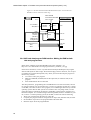
The standard memory read procedure would now be explained. The configuration is very
similar to program read, instead of using /PSEN for accessing the ROM, it uses /RD and
/WR to access the RAM. As you may aware that RAM is “read” and “write” allowed,
therefore two pins are designated for data memory interface. Here are the block diagram
and the timing diagram. As you can see address/data time multiplexing is also used here.
ALE
/PSEN
/RD
PORT0
PORT2
ALE
/PSEN
/WR
PORT0
PORT2
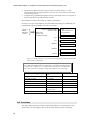
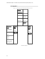
Figure 3. 6 External data memory read interface block diagram and timing diagram
9