1
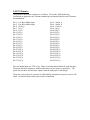
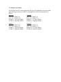
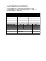
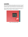
P373
Data Sheet and User Manual
PG3A Pattern Generator
P373 – LVDS probe
November 2008 - Rev 1.2
1.0 General
The P373 probe features 16 LVDS outputs running at up to 300 MHz as well as a clock
and a strobe. To preserve the signal integrity associated with the very fast risetimes
(210pS) of the output drivers, we have chosen to make the connection from the probe to
the user system via a AMP Mictor connector and a high-speed, multi-coax ribbon cable.
The probe expects the user system to be differentially terminated in a purely resistive 100
ohms. All specifications assume this resistive termination.
The two inhibit inputs are TTL levels. There is an independent inhibit for each data byte.
The probe data byte outputs are enabled when these are no-connect or pulled low. The
probe does not drive the data byte outputs when the inhibit pin is driven high.
2.0 Requirements:
The P373 probe works with all current PG3AMod and PG3ACab models. The
instrument firmware must be V1.0 or higher. The PGApp software must be V2.0.006 or
higher. Updated versions of the instrument firmware and the PGApp software can be
freely downloaded from the PG3A website: www.movingpixel.com/PG3A.html.
3.0 P373 Pinouts:
The pinout for the Mictor connector is as follows. We use the AMP numbering
convention (as opposed to the Tektronix numbering convention found in some Tektronix
documentation):
Pin 1: Low Byte Inhibit input
Pin 3: Low Byte Inhibit input
Pin 5: Clock_p
Pin 7: D1_p
Pin 9: D1_n
Pin 11: D3_p
Pin 13: D3_n
Pin 15: D5_p
Pin 17: D5_n
Pin 19: D7_p
Pin 21: D7_n
Pin 23: D9_p
Pin 25: D9_n
Pin 27: D11_p
Pin 29: D11_n
Pin 31: D13_p
Pin 33: D13_n
Pin 35: D15_p
Pin 37: D15_n
Pin 2: Strobe_p
Pin 4: Strobe_n
Pin 6: Clock_n
Pin 8: D0_p
Pin 10: D0_n
Pin 12: D2_p
Pin 14: D2_n
Pin 16: D4_p
Pin 18: D4_n
Pin 20: D6_p
Pin 22: D6_n
Pin 24: D8_p
Pin 26: D8_n
Pin 28: D10_p
Pin 30: D10_n
Pin 32: D12_p
Pin 34: D12_n
Pin 36: D14_p
Pin 38: D14_n
The two inhibit inputs are TTL levels. There is an independent inhibit for each data byte.
The probe data byte outputs are enabled when these are no-connect or pulled low. The
probe does not drive the data byte outputs when the inhibit pin is driven high.
The probe expects the user system to be differentially terminated in a purely resistive 100
ohms. All specifications assume this resistive termination.
3.1 Channel Associations
The labeling in the PG control application (PGApp or PGAppDotNet) associated with a
particular output connector on the PG correspond to the above-listed pin names as
follows:
Group A
Group B
A0[7..0] Ù Data[7..0]
B0[7..0] Ù Data[7..0]
A1[7..0] Ù Data[15..8]
B1[7..0] Ù Data[15..8]
A0(Inh) Ù Low Byte Inhibit
B0(Inh) Ù Low Byte Inhibit
A1(Inh) Ù High Byte Inhibit
B1(Inh) Ù High Byte Inhibit
Group C
C0[7..0] Ù Data[7..0]
C1[7..0] Ù Data[15..8]
C0(Inh) Ù Low Byte Inhibit
C1(Inh) Ù High Byte Inhibit
Group D
D0[7..0] Ù Data[7..0]
D1[7..0] Ù Data[15..8]
D0(Inh) Ù Low Byte Inhibit
D1(Inh) Ù High Byte Inhibit
4.0 Electrical specification for the P373 probe
All specifications assume 100 ohm differential load unless otherwise noted.
All specifications are at 25 degrees Celsius ambient temperature, 30 minutes for
stabilization of both the PG and the probe.
Characteristic
Output Risetime
Output Enable time
Output Disable time
Skew, nybble
Specification
210pS, typ
300nS max
12nS max
+/- 65pS
Notes
Skew, worst case, probeprobe
Clock before data
+/- 550pS
Output Characteristic
Vod (differential voltage)
Vcm (common mode)
Min
250mV
1.05 V
Weight
Overall Dimensions
150 grams
Length: 130mm, Width 80mm,
Height: 29mm
Yes, three hundred nS!
4 consecutive bits starting
with D0
Any bit in any probe to any
other bit in any other probe
Within one probe, all bits
50ps – 400pS typical
Typ
500mV
1.18 V
Max
600mV
1.475 V
approximate
approximate
5.0 Backside Test Connector Pinout
The P373 features a Tektronix P6980 connection from the backside to facilitate
connection to a logic analyzer during pattern debug (and perhaps even during system
test).
Pinout:
A1:
D0_p
A2: D0_n
A3:
Ground
A4:
D2_p
A5: D2_n
A6:
Ground
A7:
D4_p
A8: D4_n
A9:
Ground
A10: D6_p
A11: D6_n
A12: Ground
A13: No Connect
A14: No Connect
A15: Ground
A16: D8_p
A17: D8_n
A18: Ground
A19: D10_p
A20: D10_n
A21: Ground
A22: D12_p
A23: D12_n
A24: Ground
A25: D14_p
A26: D14_n
A27: Ground
B1:
B2:
B3:
B4:
B5:
B6:
B7:
B8:
B9:
B10:
B11:
B12:
B13:
B14:
B15:
B16:
B17:
B18:
B19:
B20:
B21:
B22:
B23:
B24:
B25:
B26:
B27:
Ground
D1_n
D1_p
Ground
D3_n
D3_p
Ground
D5_n
D5_p
Ground
D7_n
D7_p
Ground
Clock_n
Clock_p
Ground
D9_n
D9_p
Ground
D11_n
D11_p
Ground
D13_n
D13_p
Ground
D15_n
D15_p
6.0 Pre-emphasis
The P373 probe has the ability to add pre-emphasis to the output signals. There are three
jumpers accessible from the bottom of the probe that allow you to select pre-emphasis.
Pre-emphasis is useful if you are driving long, lossy wires (greater than a couple of feet).
Jumper J5: pre-emphasis control for Clock and Strobe. ON is toward the J5 silkscreen.
Jumper J3/ Jumper J2: pre-emphasis controls for the data. Both off (away from the J3/J2
reference designator silkscreen) is pre-emphasis off. Binary selection for more preemphasis (low, medium, and high). J2 is the most significant bit.
Figure 1 P373 Pre-emphasis Jumpers
7.0 Other useful information:
Part number for a connector that will mate with the probe output cable:
Amp 767054-1
Part number of the probe output cable:
Tyco/Precision Interconnect 913850038015AA21
The LVDS driver we use inside the probe is the National Semiconductor DS90LV004.
Data on this device can be found at http://cache.national.com/ds/DS/DS90LV004.pdf.
If a user system does not need to run at the highest speeds the probe supports and does
not want to connect to the user system via a Mictor, there are adapters available for
Mictor to square pins like the Nexus Technology Nex-HD20
(http://www.nexustechnology.com/products/laAccessories/hd20/).
Using an adapter from the Mictor will like cause signal integrity to suffer as the risetime
on the output of the probe is typically 210 pS. Uncontrolled impedances of longer than
5mm will be noticed in the waveform. Uncontrolled impedances of longer than 3 cm
may make the signal unusable, especially the clock signal.
Also note that all the probes except the P300 can be stacked on top of each other. Metal
inserts are provided in each side of the probe for assisting in probe mounting. The screw
thread is a UNC #4-40. Any screw thread inserted into this should not exceed 0.25
inches in length else the probe could be damaged.