1
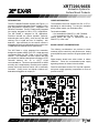
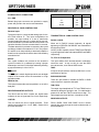
XRT7295/96ES
July 1998-3
XRT7295/96
Evaluation System
For Surface Mount Products
User Manual
Rev. 1.00
E1998
EXAR Corporation, 48720 Kato Road, Fremont, CA 94538 z (510) 668-7000 z FAX (510) 668-7017
XRT7295/96ES
NOTICE
EXAR Corporation reserves the right to make changes to the products contained in this publication in order to improve design, performance or reliability. EXAR Corporation assumes no responsibility for the use of any circuits described herein, conveys no license under any patent or other right, and makes no representation that the circuits are
free of patent infringement. Charts and schedules contained here in are only for illustration purposes and may vary
depending upon a user’s specific application. While the information in this publication has been carefully checked;
no responsibility, however, is assumed for inaccuracies.
EXAR Corporation does not recommend the use of any of its products in life support applications where the failure or
malfunction of the product can reasonably be expected to cause failure of the life support system or to significantly
affect its safety or effectiveness. Products are not authorized for use in such applications unless EXAR Corporation
receives, in writing, assurances to its satisfaction that: (a) the risk of injury or damage has been minimized; (b) the
user assumes all such risks; (c) potential liability of EXAR Corporation is adequately protected under the circumstances.
Copyright 1992 EXAR Corporation
User Manual July 1998
Reproduction, in part or whole, without the prior written consent of EXAR Corporation is prohibited.
Rev. 1.00
2
Table of Contents
INTRODUCTION . . . . . . . . . . . . . . . . . . . . . . . . . . . . . . . . . . . . . . . . . . . . . . . . . . . . . . .
5
ORDER INFORMATION . . . . . . . . . . . . . . . . . . . . . . . . . . . . . . . . . . . . . . . . . . . . . . . .
5
BOARD LAYOUT CONSIDERATIONS . . . . . . . . . . . . . . . . . . . . . . . . . . . . . . . . . . .
Figure 1. Evaluation Board . . . . . . . . . . . . . . . . . . . . . . . . . . . . . . . . . . . .
5
5
POWER SUPPLY CONNECTORS . . . . . . . . . . . . . . . . . . . . . . . . . . . . . . . . . . . . . . .
VCC RX, VCC TX, GND . . . . . . . . . . . . . . . . . . . . . . . . . . . . . . . . . . . . . . . . . . . . . .
6
6
RECEIVER I/O’S AND CONTROL PINS . . . . . . . . . . . . . . . . . . . . . . . . . . . . . . . . . .
Receiver Input . . . . . . . . . . . . . . . . . . . . . . . . . . . . . . . . . . . . . . . . . . . . . . . . . . . . .
EXCLK . . . . . . . . . . . . . . . . . . . . . . . . . . . . . . . . . . . . . . . . . . . . . . . . . . . . . . . . . . . .
ICT On/Off . . . . . . . . . . . . . . . . . . . . . . . . . . . . . . . . . . . . . . . . . . . . . . . . . . . . . . . .
REQB In/Out . . . . . . . . . . . . . . . . . . . . . . . . . . . . . . . . . . . . . . . . . . . . . . . . . . . . . .
6
6
6
6
6
RECEIVER MONITOR OUTPUTS . . . . . . . . . . . . . . . . . . . . . . . . . . . . . . . . . . . . . . . .
LOSTHR . . . . . . . . . . . . . . . . . . . . . . . . . . . . . . . . . . . . . . . . . . . . . . . . . . . . . . . . . .
Table 1. . . . . . . . . . . . . . . . . . . . . . . . . . . . . . . . . . . . . . . . . . . . . . . . . . . . .
6
6
6
TRANSMITTER I/O’s AND CONTROL PINS . . . . . . . . . . . . . . . . . . . . . . . . . . . . . .
RLOOP, LLOOP . . . . . . . . . . . . . . . . . . . . . . . . . . . . . . . . . . . . . . . . . . . . . . . . . . .
T3, STS1 or E3 Operation . . . . . . . . . . . . . . . . . . . . . . . . . . . . . . . . . . . . . . . . . .
TAOS . . . . . . . . . . . . . . . . . . . . . . . . . . . . . . . . . . . . . . . . . . . . . . . . . . . . . . . . . . . . .
ENCODIS/DECODIS . . . . . . . . . . . . . . . . . . . . . . . . . . . . . . . . . . . . . . . . . . . . . . . .
TXH1/TXL0 . . . . . . . . . . . . . . . . . . . . . . . . . . . . . . . . . . . . . . . . . . . . . . . . . . . . . . . .
6
6
6
6
6
6
RECEIVER OUTPUTS . . . . . . . . . . . . . . . . . . . . . . . . . . . . . . . . . . . . . . . . . . . . . . . . . .
6
TRANSMITTER OUTPUT . . . . . . . . . . . . . . . . . . . . . . . . . . . . . . . . . . . . . . . . . . . . . . .
7
TRANSMITTER INPUTS . . . . . . . . . . . . . . . . . . . . . . . . . . . . . . . . . . . . . . . . . . . . . . . .
7
TRANSMITTER MONITOR OUTPUTS . . . . . . . . . . . . . . . . . . . . . . . . . . . . . . . . . . .
Figure 2. Evaluation System Schematic . . . . . . . . . . . . . . . . . . . . . . . .
Table 2. XR--T7295 Demo Board Parts List . . . . . . . . . . . . . . . . . . . . .
Alternative Transformers . . . . . . . . . . . . . . . . . . . . . . . . . . . . . . . . . . . . . . . . . . .
Magnetic Supplier Information . . . . . . . . . . . . . . . . . . . . . . . . . . . . . . . . . . . . .
7
8
9
9
10
Rev.1.00
3
XRT7295/96ES
Evaluation System for
Surface Mount Products
INTRODUCTION
ORDER INFORMATION
The XR--T7295/96 Evaluation System (see Figure 1.) is
intended to facilitate and speed--up the evaluation of this
high performance DS3/STS--1/E3
Integrated Line
Receiver/Transmitter. The XR--T7295 is a fully integrated
line receiver designed for DS3 or STS--1 applications.
The XR--T7295E is designed for E3 applications.
Functions included are receive equalizer (optional),
automatic gain control (AGC), clock recovery and data
retiming, loss of signal and loss of frequency lock
detection. Input sensitivity for the receiver section is
adjustable which allows input signals at the monitor level
(--20dB below the allowed DSX--3 signal levels).
The evaluation board can emulate DS3, E3 or STS--1,
depending on switch setting. To order your evaluation
board, please contact your local sales office.
Two boards available:
-- One assembled for DS3/STS--1 (XR--T7295IW)
-- One assembled for E3 (XR--T7295--1EIW)
Please specify the type of transmission (E3 or
DS3/STS-1) in the order.
BOARD LAYOUT CONSIDERATIONS
The following considerations are provided to obtain
maximum device sensitivity and performance: Analog
ground (GNDA) must connect to the ground plane at the
pin.
The XR--T7296 is a fully integrated line transmitter
designed to operate at DS3, E3 or STS--1 data rates and
complement either the XR--T7295 or the XR--T7295E
receiver. The transmitter converts unipolar data and
clock inputs into AMI encoded pulses according to AT&T
Technical Advisory No. 34 or CCITT G.703
recommendations. This device provides B3ZS or HDB3
encoding and complimentary decoding and loopback
(remote and local) functions which can be externally
controlled. Coding errors and bipolar violations are
detected and flagged at an output pin.
Digital outputs should have series resistor to reduce
reflections. Follow the recommended power supply
bypassing scheme as shown in the schematic.
Place line termination resistor, PLL loop filter capacitor,
and power supply bypassing components as close as
possible to the IC.
Figure 1. Evaluation Board
Rev. 1.00
5
XRT7295/96ES
POWER SUPPLY CONNECTORS
LOSTHR PIN VOLTAGE
VCC
GND
VCC/2
ON
ON
VCC
ON
OFF
GND
OFF
ON
FLOAT
OFF
OFF
VCC, GND
Banana plug input connectors are provided to supply
power and ground to the receiver and transmitter.
RECEIVER I/O’S AND CONTROL PINS
Table 1.
Receiver Input
The bipolar input is a single ended analog input for the
XR--T7295 receiver IC. Two input configurations are
possible, one input method is to use a transformer
coupled system this require C1 in place and C2 removed,
the other method is to connect the line to the receiver via a
capacitor therefore C2 must a mounted and C1 removed.
The data rate at this input must correspond to the crystal
oscillator provided in the locations X1 or X2. The jumpers
E1 and E2 are for the possibility to electrically isolate the
board from the system and have the demo board floating
towards the line.
TRANSMITTER I/O’s AND CONTROL PINS
RLOOP, LLOOP
When set for RLOOP (remote loopback), all signals
appearing on RPDATA and RNDATA are transmitted to
the line using RCLK.
LLOOP (Local Loopback) causes TPDATA and TNDATA
to go through the encoder and output at RPOS and RNEG
respectively.
T3, STS1 or E3 Operation
EXCLK
This input selects which encoder/decoder combination
should be used. A high on this pin sets the B3ZS
encoder/encoder, a low selects HDB3 mode.
Two crystal oscillators are provided on the board the
crystal in location X1 is selected by inserting a jumper
between pin 1 and 2 on P3, X2 will be selected by inserting
a jumper between pin 2 and 3 of P3.
TAOS
ICT On/Off
A high on this pin causes a continuous AMI of all 1’s to be
transmitted on the line.
The ICT input is a static digital input which sets all digital
outputs of the receiver and/or the transmitter in a high
impedance state.
ENCODIS/DECODIS
REQB In/Out
These two pins enable or disable the B3ZS or HDB3
coders from their respective data path.
This input pin selects the receive equalizer in or out of the
data path.
TXH1/TXL0
The output signal amplitude at TTIP and TRING can be
selected by taking this pin high or low. For cable lengths
greater than 225 feet TXLEV should be set high. For
cable lengths less than 225 feet, it should be set low.
RECEIVER MONITOR OUTPUTS
The RLOS and the RLOL outputs are digital status
indicators for loss of signal and loss of lock, respectively.
LOSTHR
RECEIVER OUTPUTS
This pin controls the loss of signal threshold. Three
settings are provided (VCC, VCC/2, GND). Setting of this
pin works as follows:
RPOS, RNEG, RCLK AND RNRZ are the receiver
outputs after going through the receive side decoder of
the transmitter IC.
Rev. 1.00
6
XRT7295/96ES
TRANSMITTER OUTPUT
TRANSMITTER MONITOR OUTPUTS
This is a bipolar output signal to be transmitted to the line
through a 1:1 transformer from the TTIP and TRING
outputs. The output signal complies to the AT&T TA #34
or G.703 pulse template.
Bipolar Violations (BVP) and Driver Monitor (DMO)
outputs are digital status indicators.
The Bipolar
Violations pin goes high for one bit period when a bipolar
violation or coding error is detected in the received signal.
TRANSMITTER INPUTS
The driver monitor circuit monitor senses the transmitted
signals at MTIP/MRING and goes high if there is no
transmitted signal for 128+/--32 TCLK periods.
These are dual rail NRZ data signals which correspond to
the bipolar data to be transmitted to the line. TPDATA and
TNDATA are both sampled on the falling edge of TCLK
and can be tied together for binary input signals.
Rev. 1.00
7
E1
R1
75
VCC
OE1
R2
75
OE2
R4
22K
1
R3
22K
1
Oe
X2
20
BD1
GNDC
8
VCC
4
4
5
51.84 MHz
Fo
44.736 MHz
0.1 F
C5
Fosc
0.1 F
C4
GND
+5V
+
VCC
0.1 F
C7
C10
22 F
0.1 F
C11
VCC
J3
J4
J5
R9 36.5
R1036.5
R1136.5
R14
75
R13
75
R12
75
TRANSMITER
MONITOR
OUTPUTS
DMO
BPV
TPDATA
TNDATA
TCLK
REQB
ICTN
RCLK
RNDATA
RPDATA
19
C8
24
Ferrite bead
0.1 F
C9
6
21
GNDA
DMO
BPV
MTIP 20
MRING
10
BD2
22
TRING
TTIP 23
14
15
RNRZ
RNEG
GNDD
TPDATA
TNDATA
TCLK
RPOS 16
RCLKO 17
RLOOP
LLOOP
DS3,STS--1/E3/
TAOS
TXLEV
ICT/
ENCODIS
DECODIS
2
3
4
5
25
26
11
12
R15 R16 R17R18
R19 R20 R21 R22
U2
XR--T7296
RCLK
RNDATA
RPDATA
0.1 F
18
13
7
8
9
1
28
27
RPDATA
RNDATA
RCLK
R7 R8 R6 R5
22K
LOSTHR
Ferrite Bead # Fair Rite 2743019446
Transformer # Pulse Engineering PE 68629
PE 65967 In Surface Mount
Figure 2. Evaluation System Schematic
P2
P1
Ferrite bead
C6
0.1 F
1211
9
10
1
6
GNDA
3
TMC2
19
18
17
14
15
16
4 3 2 1
5 6 7 8
REQB
ICT
LOST
TMC1
8
LPF1
EXCLK
RIN
RLOL
RLOS
LOSTHR
REQB
ICT/
RCLK
RNDATA
RPDATA
GNDD
5
13
LP1 4
C3
RIN
2
8
7
U1
XR--T7295
0.1 F
5 LPF2
LP2
Fo
0.01 F
RLOL
S1
SW DIP--4
VCC
C1
X1
Oe
C2
0.01 F
Install C1 or C2
2 way Jumper
1
2
3
P3
J2
JUMPER
T1
PE 68629
Vcc
GND
Input
Signal
J1
RLOS
RLOS RLOL
Outputs
Receiver
Monitor
VDDA
GND Vcc
VDDC
VDDD
8
VDDA
Rev. 1.00
VDDD
VCC
VCC
R26270
R25 270
VCC
GND
GND
GND
GND
GND
GND
R24 36.5
R23 36.5
RNZR
RNEG
RPOS
1
2
3
4
5
6
7
8
S2
Spare
SW DIP--8
22K
RCLKO
Spare
16
15
14
13
12
11
10
9
RLOOP
LLOOP
T3/E3
TAOS
TXLEV
ICT
ENCODIS
DECODIS
TRING
TTIP J6
E2
JUMPER
PE 68629
T2
OUTPUTS
RECEIVER
J7
XRT7295/96ES
XRT7295/96ES
QTY
REFERENCE
DESCRIPTION
SUPPLIER
2
T1,2
Transformer, 1:1 Ratio
Pulse Corp. PE--68629
5
R1,2,12,13,14
75 , 1/8 W, 1%, 1206 Size, Chip Resistor,
Panasonic
Digikey P75.0FCT--ND (Bulk
Packed)
14
R3,4,5,6,7,8,15,16,
17,18,19,20,21,22
22.1K, 1/8 W, 1%, 1206 Size, Chip Resistor, Panasonic
Digikey P22.1KFCT--ND (Bulk
Packed)
5
R9,10,11,23,24
36.5 , 1/8 W, 1%, 1206 Size, Chip Resistor, Panasonic
Digikey P36.5KFCT--ND (Bulk
Packed)
2
R25,25
274 , 1/8 W, 1%, 1206 Size, Chip Resistor, Panasonic
Digikey P274CT--ND (Bulk
Packed)
2
C1,2
0.01 F, 63V, X7R Dilectric,
Axial lead, 0.1” Spacing (Thru--hole),
Panasonic
Digikey P4881--ND
8
C3,4,5,6,7,8,9,11
0.1 F, 50V, X7R Dilectric,Chip Capacitor,
Panasonic
Digikey PCC104BCT--ND
1
C10
22 f, 16V Electrolytic Cap., Radial lead,
0.1” spacing (Thru--hole)
Digi--key P5228
2
BD1,2
SMT ferrite bead
Fair--Rite Products 2743019446
7
J1,2,3,4,5,6,7
PC board mount BNC Connector
H&P 44FO794
1
X1
44.736MHz Osc. Module -- Tristate
(DS3/STS1 Unit, XR--T7295)
Monitor Products 975HHT
1
X2
51.84MHz Osc. Module -- Tristate
(DS3/STS1 Unit, XR--T7295)
Monitor Products 975HHT
1
X1
34.368MHz Osc. Module
(E3 Unit, XR--T7295E)
Monitor Products 975HHT or
975H (not tri--satate)
1
S1
4--SECTION DIP SWITCH
Digi--key CT--2064
1
S2
8--SECTION DIP SWITCH
Digi--key CT--2068
1
E1,E2
Shorting jumper (shunt)
(Oscillator Selection)
1
P3
3 pin single--row header, gold
Digi--key S9002--ND
18
TP1 to TP18
Pins for Test Point connections
Digi--key ED--5052--ND
2
P1,P2
Banana Jacks (1 Black and 1 Red)
Digi--key J151--ND
4
Spacers to elevate board
4
4--40 x 5/16” screws for spacers
Table 2. XR--T7295 Demo Board Parts List
Alternative Transformers
PULSE PE65966
PULSE PE65967 (Surface mount)
TTI
7170
Rev. 1.00
9
XRT7295/96ES
Magnetic Supplier Information
Transpower Technologies, Inc.
24 Highway 28, Suite 202
Crystal Bay, NV 89402-0187
Tel. (702) 831-0140
Fax. (702) 831-3521
Pulse
Telecom Product Group
P.O. Box 12235
San Diego, CA 92112
Tel. (619) 674-8100
Fax. (619) 674-8262
Fair-Rite Products Corp.
P.O. Box J
One Commercial Row
Wallkill, NY 12589
Tel. (914) 895-2055
Fax. (914) 895-2629
E-Mail. [email protected]
Rev. 1.00
10
EXAR Corporation
48720 Kato Road
Fremont, CA 94538
(510) 668-7000, Fax (510) 668-7017
Worldwide Web Site: http://www.exar.com
Rev. 1.00
E1992