1
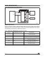
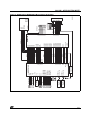
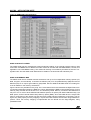
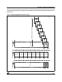
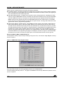
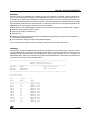
AN1386 APPLICATION NOTE Using the DSM2180F3 with the Analog Devices ADSP-2185 CONTENTS ■ PURPOSE ■ DSM2180F3 ARCHITECTURE ■ DEVELOPMENT SYSTEMS ■ INTERFACING THE DSM2180F3 WITH THE ADSP-2185 – DSM2180F3 Bus Interface – ADSP-218X to DSM2180F3 Schematic ■ DEFINE THE ADSP-2185 INTERFACE IN PSDSOFT EXPRESS ■ ADSP-2185 BOOT LOADER ■ ADSP-2185 MEMORY MAP ■ PROGRAMMING THE DSM2180F3 IN-CIRCUIT USING THE JTAG INTERFACE ■ SUMMARY ■ APPENDIX The DSM2180F3 is a system memory device for use with Digital Signal Processors from the popular Analog Devices ADSP218X family. DSM means Digital signal processor System Memory. A DSM device brings In-System Programmable (ISP) Flash memory, programmable logic, and additional I/O to DSP systems. The result is a simple and flexible two-chip solution for DSP designs. DSM devices provide the flexibility of Flash memory and smart JTAG programming techniques for both manufacturing and the field. On-chip integrated memory decode logic and memory paging logic make it easy to add large amounts of external Flash memory to the ADSP-218X family for bootloading and/or overlay memory. The DSP accesses this Flash memory using either its Byte DMA (BDMA) interface or as external data overlay memory (no DMA setup overhead). JTAG In-System Programming (ISP) reduces development time, simplifies manufacturing flow, and lowers the cost of field upgrades. The JTAG ISP interface eliminates the need for sockets and pre-programmed memory and logic devices. For manufacturing, end products may be assembled with a blank DSM device soldered to the circuit board and programmed quickly. In addition to ISP Flash memory, DSM devices add programmable logic (PLD) and up to 16 configurable I/O pins to the DSP system. The state of each I/O pin can be driven by DSP software or PLD logic. PLD and I/O configuration are programmable by JTAG ISP, just like the Flash memory. The PLD consists of more than 3000 gates and has 16 macro cell registers. Common uses for the PLD include chip selects for external devices, state-machines, simple shifters and counters, keypad and control panel interfaces, clock dividers, handshake delay, and muxes. This eliminates the need for small external PLDs and logic devices. Configuration of PLD, I/O, and Flash memory mapping are easily entered in a point-and-click environment using the software development tool, PSDsoft Express™. This software is available at no charge from http://www.psdst.com/ html/softcenter2.html. The two-chip combination of a DSP and a DSM device is ideal for systems that have limitations on physical size and power consumption concerns. DSM memory and logic are “zero-power,” meaning they automatically go to standby between memory accesses or logic input changes, producing low active and standby current consumption. June 2001 1/17 AN1386 - APPLICATION NOTE PURPOSE The DSM2180F3 device is designed to interface directly with the popular Analog Devices ADSP-218X series of DSPs. The DSM2180F3 device provides bootloading capability and enables the core DSP design to be done with two chips. The DSM JTAG port allows In-System Programming (ISP) of a completely blank DSM2180F3 device soldered to the board with no involvement of the DSP, which is ideal for first time programming during manufacturing. Subsequent field updates can also be done via this interface. This application note addresses the ease of interfacing the DSM2180F3 with the ADSP-2185 DSP. Familiarity with the DSM2180F3 is assumed. Please see the DSM2180F3 data sheet for a detailed description of the device. DSM2180F3 ARCHITECTURE Figure 1 is a block diagram of the DSM2180F3. Figure 1. DSM2180F3 Block Diagram INTERNAL ADDR, DATA, CONTROL BUS LINKED TO DSP SECURITY LOCK FLASH MEMORY PAGE REG DECODE PLD (DPLD) DSP ADDR FS0-7 PA0 PA1 PA2 PA3 PA4 PA5 PA6 PA7 RUNTIME CONTROL CSIOP REGISTER CSIOP POWER MANAGEMENT I/O PORT EXTERNAL CHIP SELECTS, ESC0-2 EXTERNAL CHIP SELECTS 3 OPTIONAL OUTPUTS TO PORT D COMPLEX PLD (CPLD) AND ARRAY DSP CONTROL CNTL0 CNTL1 CNTL2 PD0 PD1 PD2 RST\ DSP DATA 8 SEGMENTS, 16 KB 128 KBytes TOTAL PLD INPUT BUS AD0 AD1 AD2 AD3 AD4 AD5 AD6 AD7 AD8 AD9 AD10 AD11 AD12 AD13 AD14 AD15 PC2 PC7 fs7 fs6 fs5 fs4 fs3 fs2 fs1 fs0 DSM2180F3 DSP SYSTEM MEMORY B B B B B B B B B B B B B B B B C C C C C C C C 16 OUTPUT MICRO<>CELLS B B B B B B B B C C C C C C C C ALLOCATOR I/O PORT PC0 PC1 16 INPUT MICRO<>CELLS PIN FEEDBACK NODE FEEDBACK PB0 PB1 PB2 PB3 PB4 PB5 PB6 PB7 JTAG-ISP TO ALL AREAS OF CHIP PC3 PC4 PC5 PC6 AI04951 On-chip features supply the key elements to implement a two-chip DSP System. Flash DSM features include: ■ Glueless connection to DSP: easily add memory, logic, and I/O to DSP. 2/17 AN1386 - APPLICATION NOTE ■ 128 KBytes of main Flash memory, divided into eight equal individually protected sectors. ■ Flash-based PLD with 16 Output Macrocells and 16 Input Macrocells. ■ General Purpose PLD that is configurable for external chip-selects or combinatorial logic. ■ 19 individually configurable I/O Port pins. Each may be defined as DSP I/Os, PLD I/Os, latched DSP address outputs, or special function I/Os. ■ 8-bit Page Register to expand the external address space and implement memory swapping. ■ JTAG compliant serial port for true In-System Programming (ISP) of blank devices and reprogramming of devices in the factory or field. DEVELOPMENT SYSTEMS This application note provides general guidelines for connecting the DSM2180F3 to the ADSP-218X DSP. In addition, ST provides a specific development kit implementation called the DK-2180 that highlights many of the features of the DSM and ADSP. For more information, see our development kit section of our website: http://www.psdst.com/html/tools.html. PSDsoft Express is a software development tool that runs on Windows platforms for DSM family development. This tool allows you to configure the DSM using a simple point-and-click interface. DSP bootloader firmware is imported and merged to create a single programming data file (.obj) to program into the DSM. The generated programming data file is then used to program the DSM using one of ST’s programmers (PSDpro or FlashLINK) or a 3rd party programmer. For more information on PSDsoft Express, visit http:/ /www.psdst.com/html/softcenter2.html. To see a list of compatible 3rd party programmers, visit http:// www.psdst.com/html/psdprog.html. INTERFACING THE DSM2180F3 WITH THE ADSP-2185 The ADSP-2185 contains the following: ■ An on-chip 8-bit Automatic Boot Loader through DMA interface or memory port ■ 80 KBytes RAM configures as: ■ 16 KWords Program Memory RAM (24-bit) ■ 16 KWords Data Memory RAM (16-bit) ■ Dual-purpose Program Memory for both instructions and data storage. The low-cost DSM2180F3 is selected for this design to take advantage of the ADSP-2185 resident boot loader, using its Flash memory to store the downloadable ADSP-2185 program code. Figure 2 is a basic block diagram that shows the implementation of a basic system using the DSM2180F3/ ADSP-2185 two-chip combination. All glue logic, Flash memory, bus interface logic, I/O, chip selects, and PLDs are contained in the DSM chip. 3/17 AN1386 - APPLICATION NOTE Figure 2. Minimized DSP System Block Diagram Optional Device D8-D15 A0-A15 Control Lines AD0-AD15 Port A Address Control LCD, UART, etc. CNTL[2..0] Port B Port C ADSP-2185 Data DMS2180 JTAG Header Port D AI04952 DSM2180F3 Bus Interface When an ADSP218x is selected in PSDsoft Express (see Section 6), the bus interface is pre-configured so there is no chance to make a configuration mistake. Table 2 lists the bus interface signals from the ADSP-2185 used to access the Flash memory, PLD logic, and I/O inside the DSM2180F3. These signals are automatically configured when the ADSP-218X is selected. Table 1. ADSP-2185 / DSM2180F3 Bus Interface Pin Functions ADSP-2185 Pin Functions A [15:0] ADIO [15:0] D [7:0] N.C. D [15:8] Port A:PA [7:0] /WR /RD /BMS /RESET 4/17 DSM2180F3 Pin Functions CNTL0 CNTL1 CNTL2 _RESET Pin Description External Address Bus addresses all external memory - Program, Data and I/O. 8 high byte bi-directional external Data bus lines. 8 low byte bi-directional external Data bus lines.Port A is used as the 8-bit Data bus into the DSM2180F3. Write signal is used to access external memory during memory write cycles. Read signal is used to access external memory during memory read cycles. Byte Memory Select signal is used for external 8-bit data memory accesses. System reset input D18 D19 _RESET PWDACK _RESET uP Supervisor SPORT1 SERIAL CHN Serial Device VCC SPORT0 SERIAL CHN A8 A9 A10 A11 A12 A13 D16 D17 A0 A1 A2 A3 A4 A5 A6 A7 _WR _RD _BMS _IOMS _DMS _PMS _CMS ADSP-218X PF0/MODEA PF1/MODEB PF2/MOCEC PF3 _IRQE/PF4 _IRQL0/PF5 _IRQL1/PF6 _IRQ2/PF7 FL0 FL1 FL2 XTAL CLKIN _PWD _BR _BG _BGH Serial Device I/O I/O I/O I/O INTR/I_O INTR/I_O INTR/I_O INTR/I_O I/O I/O I/O Oscillator or XTAL PWR_DOWN_IN BUS_REQUEST BUS_GRANT GRANT_HUNG D8 D9 D10 D11 D12 D13 D14 D15 N/C N/C _RESET POWER DOWN ADDR16 ADDR17 ADDR8 ADDR9 ADDR10 ADDR11 ADDR12 ADDR13 ADDR14 ADDR15 ADDR0 ADDR1 ADDR2 ADDR3 ADDR4 ADDR5 ADDR6 ADDR7 WRITE READ BYTE MEM SELECT I/O MEM SELECT DATA MEM SELECT DATA8 DATA9 DATA10 DATA11 DATA12 DATA13 DATA14 DATA15 PD2/_CSI _RESET PC2 PC7 ADIO8 ADIO9 ADIO10 ADIO11 ADIO12 ADIO13 ADIO14 ADIO15 ADIO0 ADIO1 ADIO2 ADIO3 ADIO4 ADIO5 ADIO6 ADIO7 CNTL0 CNTL1 CNTL2 PD0 PD1 PA0 PA1 PA2 PA3 PA4 PA5 PA6 PA7 PC0 PC1 PC3 PC4 PC5 PC6 PB0 PB1 PB2 PB3 PB4 PB5 PB6 PB7 DSM2180 TMS TCK TSTAT _TERR TDI TDO I/O I/O I/O I/O I/O I/O I/O _RESET VCC CHIP SELECT _SELECT GND VCC Optional Device LCD, UART, etc. ADDRESS _WR _RD DATA AI04953 Optional JTAG Header DATA8..15 WRITE READ ADDR0..2 AN1386 - APPLICATION NOTE Figure 3. ADSP-218x to DSM2180F3 Bus Interface Schematic 5/17 AN1386 - APPLICATION NOTE ADSP-218X to DSM2180F3 Schematic Figure 3 shows an example schematic diagram for an ADSP-218x to DSM2180F3 design. While Table 1 shows the required connections for every design, the schematic shows additional signals and functions that would be typical of many designs. Specifically, the following signals have been added: Table 2. ADSP-2185 / DSM2180F3 Optional Signals Used ADSP-2185 Pin Functions DSM2180F3 Pin Functions Pin Description /IOMS PD0 I/O Memory Select signal /DSM PD1 Data Memory Select signal D18 PC2 Address bit 16 D19 PC7 Address bit 17 PWDACK N/A PD2/_CSI PB2 Power down chip select signal Chip Select for external device, such as LCD, UART, etc. Note: The schematic also shows basic ADSP-218x connections, such as the system reset input and the DSM2180F3 shows additional optional connections, such as I/O and JTAG. DEFINE THE ADSP-2185 INTERFACE IN PSDSOFT EXPRESS Highlights of design entry will be given here. Please refer to the PSDsoft Express User Manual for a thorough coverage of all the features of PSDsoft Express. This section is meant to show you just the essentials to get you going. Here are the steps when using a template: Invoke PSDsoft Express and Open a New Project ■ Start PSDsoft Express. ■ Create a new project. ■ Select your project folder and name the project (in this example, name the project “DSM2180” in the folder PSDsoft\my_project). The associated dialog box is shown graphically in Figure 4. MCU/DSP and PSD Selection When you click OK in the “New Project” window, the “MCU and PSD Selection” screen appears. When you see this screen, make the following selections: ■ Select Analog Devices for the manufacturer and ADSP 218x for the type ■ The control signals are selected for you. ■ Select the DSM2180 for the Family, the DSM2180F3 for the part and the K package. ■ The MCU/DSP parameters are set for you. Click OK. 6/17 AN1386 - APPLICATION NOTE Figure 4. PSDsoft Express Define DSM and MCU/DSP Now you have your project established based on a DSM2180F3 and an ADSP-2185. When the “Design Parameters” screen appears, choose “Use example template selection” and click OK to be taken to the “MCU Template Selection” screen. Now choose “Application Note 076, DSP loader” and click Generate. This will automatically setup the extra pins described in Table 2 and the memory map described in the next section Pin Definitions Your pin definitions should match Figure 5 and are defined according to the schematic shown in Figure 3. On this screen, you can add or update pin functionality as desired. When you are finished, clicking Next>> will take you to the “Design Assistant” screen, which will be covered in the next section. 7/17 AN1386 - APPLICATION NOTE Figure 5. DSM2180F3 Pin Definitions Note: There are detailed instructions on how to use this screen and other screens in the PSDsoft Express User Manual. ADSP-2185 BOOT LOADER The ADSP-2185 has two mechanisms to allow automatic loading of the internal program memory after reset which are BDMA boot or IDMA boot. Either mode can be used with the DSM2180F3, however, this application note uses BDMA booting. The method for booting is controlled by the Mode A, B and C configuration bits. See the ADSP-2185 data sheet for details on the boot methods and Mode pins. ADSP-2185 MEMORY MAP The ADSP-2185 uses a modified Harvard architecture with up to four independent memory spaces (I/O, Data, Program, and Combined). It contains 16 KWords (x16) of on-chip Data Memory (DM) Ram and 16 KWords (x24) of on-chip Program Memory (PM) RAM. See the ADSP-2185 data sheet from Analog Devices for details on the memory architecture. Figure 6 shows one possible memory map. The nomenclature fs0.fs7 are individual 16 KByte Flash memory segment designators within the DSM and “csiop” designates the DSM control register block. For this memory map, the DSP should be set to run in Full Memory Mode. Memory contents of the DSM device may lie in one or more of three different DSP address spaces; I/O space (with limited address lines), byte DMA space, and/or External Data-overlay Memory Space (DMS). Since the DSM device is a byte-wide memory, awareness of the natural x16 and x24 nature of DM and PM respectively is important. The designer may easily specify memory mapping in a point-and-click software environment using PSDsoft Express™. Since the memory mapping is implemented with the DPLD and the Page Register, many possibilities exist. 8/17 000FF 00000 00208 00200 1FFFF 256 CONTROL REGS csiop 8 UART REGS _cs_uart Nothing Mapped DSP I/O Memory Space (IOMS) 00000 03FFF 04000 07FFF 08000 0BFFF 0C000 0FFFF 10000 13FFF 14000 17FFF 18000 1BFFF 1C000 1FFFF 16K Bytes Flash Memory fs0 16K Bytes Flash Memory fs1 16K Bytes Flash Memory fs2 16K Bytes Flash Memory fs3 16K Bytes Flash Memory fs4 16K Bytes Flash Memory fs5 16K Bytes Flash Memory fs6 16K Bytes Flash Memory fs7 DSP Byte DMA Memory Space (BMS) 00000 03FFF A13 = 1 16K Bytes A13 = 0 (8K Words) fs0 PAGE 0 PAGE 1 Nothing Mapped A13 = 0 fs1 A13 = 1 A13 = 0 fs2 A13 = 1 PAGE 3 A13 = 0 fs3 A13 = 1 PAGE 4 A13 = 0 fs4 A13 = 1 PAGE 5 PAGE 6 A13 = 1 A13 = 0 fs5 Flash Memory Paged Over 8 Pages PAGE 2 1FFFF DSP Data Memory Space (DMS) A13 = 0 fs6 A13 = 1 PAGE 7 A13 = 0 fs7 A13 = 1 AI04956 00000 03FFF AN1386 - APPLICATION NOTE The memory map is organized to work within the restrictions of the ADSP-2185 Boot Loader (discussed in the previous section) and to utilize the entire Flash memory and show the paging features of the DSM2180F3. Figure 6. ADSP-2185/DSM2180F3 Memory Map 9/17 AN1386 - APPLICATION NOTE Figure 6 shows a typical memory map with the following attributes: ■ I/O Address Space. The 256 byte locations for DSM control registers (csiop) reside in DSP I/O address space, selected by the DSP IOMS signal. Since DSP I/O accesses are 16 bits, not 8 bits, the upper byte of a 16-bit DSP I/O access must be ignored. ■ Byte DMA Address Space. The DSP may boot-load or fetch overlay bytes from 128 KBytes of Flash memory using the DSP BDMA channel. The DSP may also write to Flash memory using the Byte DMA channel. DSM Flash memory is accessed in 128 KB continuous byte address locations through the BDMA channel and is selected whenever the DSP BMS signal is active. Flash memory in the DSM device must be un-locked and written by the DSP one byte at a time, checking status after each write (typical Flash memory programming algorithm). ■ Data Overlay Memory Address Space. All 128 KBytes of Flash memory also reside in DSP External Data-overlay Memory Space, selected by DMS, allowing more efficient byte writes to Flash memory. The DSP uses its external data overlay window of 8 KB locations to access external memory as data. The DSP doubles the size of this window to 16 KB locations by manipulating its A13 address line using its DMOVLAY register (See the ADSP-2185 data sheet for details). Since all 128 KBytes of Flash memory must be accessed through a window of only 16 KB locations, the DSP uses the Page Register inside the DSM device to page through 8 pages of 16 KBytes, as shown in Figure 6. Since DSP Data accesses are by 16 bits, not 8 bits, the upper byte of a 16-bit DSP Data access must be ignored. Define the Memory Map in PSDsoft Express The template’s memory map is setup according to Figure 6. First, note how the Page Register is setup, shown in Figure 7. Figure 7. DSM2180F3 Page Register Setup The memory map is organized to work within the restrictions of the ADSP-2185 Boot Loader and to utilize the entire Flash memory and show the paging features of the DSM2180F3. The three paging bits will provide 23 = 8 pages. Click Next to see the Chip Selection Equations screen, shown in Figure 8. 10/17 AN1386 - APPLICATION NOTE Figure 8. DSM2180F3 Chip Select Equations If you click on each of the chip select signals in the list on the list, you will see that they have all been defined according to the memory map in Figure 6. Note that all the chip-select equations are listed in the Appendix. The I/O Logic Equations and User-defined Equations tabs are used to implement general-purpose combinatorial and sequential logic. These topics are covered in more detail in the PSDsoft Express User Manual: http://www.psdst.com/html/psdsoft_exp.htm. When you are ready to see how the DSP firmware can be loaded into the DSM via the programming data file (.obj), click Done. Loading the ADSP Firmware into the DSM Now that you have completed the definitions of the DSM’s internal and external signals, it is time to load the ADSP firmware into the DSM. To accomplish this, take the following steps: ■ Click the Fit Design to Silicon button in the PSDsoft Express design flow. Since this is a template, the design should fit without errors if you have not modified the design. If you do get an error, you will need to fix it before moving on. ■ Take note of the Generate C Code button. It is used to generate flash routines that can be pasted into your C Code before compiling and linking. This is not required for the presented design. ■ Click the Merge MCU/DSP firmware with PSD button. This step is where the DSM configuration/mem map are merged with the output of the compiler/linker tools chain. Upon invocation, you will get a warning that basically says, since paging was used in the design, the software is not sure how to fill in the file start and stop addresses and you will have to do it manually. Figure 9 shows an example of how this might be filled in and assumes that a file called “Program.hex” has been previously generated, taking up the first three DSM flash segments. Note the scroll bar on the right to access memory beyond fs3. Click OK to generate the programming data file (.obj) that will be used to program the device. That's it; you are now ready to program the device. For more information on how to program the DSM through the JTAG port or a conventional programmer, consult the PSDsoft Express User Manual: http:// www.psdst.com/html/psdsoft_exp.htm. 11/17 AN1386 - APPLICATION NOTE Figure 9. Merging of DSP Firmware with DSM Memory Map PROGRAMMING THE DSM2180F3 IN-CIRCUIT USING THE JTAG INTERFACE The ability to initially program a new system board with a blank Flash memory soldered directly to it has solved many manufacturing logistics problems: no sockets or individual labels are required; inventory of non-volatile program memory chips is reduced to one package; the PLD is programmed at the same time as the memory chip: one system board can be built and inventoried; and options can be programmed into the Flash memory at board level testing. Port C I/O lines are used to interface to the standard JTAG signals - TMS, TCK, TDI and TDO. TSTAT and TERR are optional JTAG-ISP extensions that can be monitored to decrease the programming time of the DSM2180F3. The DSM configuration, PLD logic, and Flash memory can all be programmed through the JTAG port. Port C JTAG pins can also be multiplexed with other signals, such that the signals are used to program the DSM while the DSP is held in reset and as general I/O during normal DSP operation. The cost of JTAG muxing is a single pin on the DSM to control the state of this mux. This option frees up the JTAG pins for I/O functions after JTAG programming is complete. For more information on how the JTAG port can be multiplexed, see Application Note AN1153 and the PSDsoft Express User Manual at: http://www.psdst.com/html/psdsoft_exp.htm. Also note that the DK-2180 development board multiplexes the JTAG signals and has a slightly different pin configuration. 12/17 AN1386 - APPLICATION NOTE SUMMARY As DSPs continue to proliferate into markets such as communications, industrial, medical, signal conditioning, and hand held test equipment, the DSM2180F3 and DSP form an ideal 2-chip solution with onchip PLD and I/O lines that are individually configured to perform any function required by the system design. Using the DSM2180F3 as an 8-bit boot loader in both high speed and low speed systems is an ideal and rapid design alternative to a discrete solution. Inexpensive slower memory and PLDs integrated in the DSM2180F3 now become both cost and performance effective. Several features of the DSM2180F3 were used to expand the functionality of the ADSP-2185, including: ■ In-System Programmable Flash memory. ■ JTAG-ISP to simplify manufacturing. ■ Expanded I/O. ■ Interfacing to external devices was easily accomplished by generating the required control signals in the internal programmable PLD. ■ A quick and easy design prototype using PSDsoft Express. These changes have added to both the versatility and performance of the ADSP-2185. APPENDIX The Appendix contains the PSDsoft Express Design Assistant Summary listing all logic equations to show how the DSM2180F3 is configured for the ADSP-2185 interface in order to implement the example in this Application Note. Application Note AN1356 presents a step-by-step illustration of how to configure the Flash DSM Family. Although AN1356 uses the 16-bit Flash PSD4235G2 in the example, the software and procedure is the same for the 8-bit DSM2180F3. *********************************************************************** PSDsoft Express Version 7.10 Summary of Design Assistant *********************************************************************** PROJECT : AN076 DATE : 05/21/2001 DEVICE : DSM2180F3 TIME : 13:05:59 MCU/DSP : ADSP-218x *********************************************************************** Pin Definitions: ================ Pin Name -----------adio0 adio1 adio2 adio3 adio4 adio5 adio6 adio7 adio8 adio9 adio10 adio11 adio12 Signal Name -----------a0 a1 a2 a3 a4 a5 a6 a7 a8 a9 a10 a11 a12 Pin Type -----------Address line Address line Address line Address line Address line Address line Address line Address line Address line Address line Address line Address line Address line 13/17 AN1386 - APPLICATION NOTE adio13 adio14 adio15 cntl0 cntl2 cntl1 reset pa0 pa1 pa2 pa3 pa4 pa5 pa6 pa7 pb0 pc0 pc1 pc2 pc3 pc4 pc5 pc6 pc7 pd0 pd1 pd2 a13 a14 a15 _wr _bms _rd _reset d8 d9 d10 d11 d12 d13 d14 d15 _cs_uart tms tck a16 tstat _terr tdi tdo a17 _ioms _dms _csi Address line Address line Address line DSP bus control signal DSP bus control signal DSP bus control signal RESET input Data line Data line Data line Data line Data line Data line Data line Data line External chip select - Active-Lo Dedicated JTAG - TMS Dedicated JTAG - TCK Logic or address Dedicated JTAG - TSTAT Dedicated JTAG - /TERR Dedicated JTAG - TDI Dedicated JTAG - TDO Logic or address Logic or address Logic or address PSD chip select input, /CSI User defined nodes: =================== None defined Page Register settings: ======================= pgr0 is used for paging pgr1 is used for paging pgr2 is used for paging pgr3 is not used pgr4 is not used pgr5 is not used pgr6 is not used pgr7 is not used Equations: ========== csiop = ((address >= ^h0000) & (address <= ^h00FF) & (!_ioms & _dms & _bms)); fs0 = ((address >= ^h0000) & (address <= ^h3FFF) & (_ioms & _dms & !_bms)) # ((page == 0) & (address >= ^h0000) & (address <= ^h3FFF) & (_ioms & !_dms fs1 = ((address >= ^h4000) & (address <= ^h7FFF) & (_ioms & _dms & !_bms)) # ((page == 1) & (address >= ^h0000) & (address <= ^h3FFF) & (_ioms & !_dms fs2 = ((address >= ^h8000) & (address <= ^hBFFF) & (_ioms & _dms & !_bms)) # ((page == 2) & (address >= ^h0000) & (address <= ^h3FFF) & (_ioms & !_dms fs3 = ((address >= ^hC000) & (address <= ^hFFFF) & (_ioms & _dms & !_bms)) # ((page == 3) & (address >= ^h0000) & (address <= ^h3FFF) & (_ioms & !_dms fs4 = ((address >= ^h10000) & (address <= ^h13FFF) & (_ioms & _dms & !_bms)) # ((page == 4) & (address >= ^h0000) & (address <= ^h3FFF) & (_ioms & !_dms fs5 = ((address >= ^h14000) & (address <= ^h17FFF) & (_ioms & _dms & !_bms)) 14/17 & _bms)); & _bms)); & _bms)); & _bms)); & _bms)); AN1386 - APPLICATION NOTE # ((page == 5) & (address >= ^h0000) & (address <= ^h3FFF) & (_ioms & !_dms & _bms)); fs6 = ((address >= ^h18000) & (address <= ^h1BFFF) & (_ioms & _dms & !_bms)) # ((page == 6) & (address >= ^h0000) & (address <= ^h3FFF) & (_ioms & !_dms & _bms)); fs7 = ((address >= ^h1C000) & (address <= ^h1FFFF) & (_ioms & _dms & !_bms)) # ((page == 7) & (address >= ^h0000) & (address <= ^h3FFF) & (_ioms & !_dms & _bms)); !_external_cs = ((address >= ^h0200) & (address <= ^h0207) & (!_ioms & _dms & _bms)); 15/17 AN1386 - APPLICATION NOTE Table 3. Document Revision History Date Rev. 21-Jun-2001 1.0 16/17 Description of Revision Document written AN1386 - APPLICATION NOTE For current information on PSD products, please consult our pages on the world wide web: www.st.com/psd If you have any questions or suggestions concerning the matters raised in this document, please send them to the following electronic mail addresses: [email protected] [email protected] (for application support) (for general enquiries) Please remember to include your name, company, location, telephone number and fax number. Information furnished is believed to be accurate and reliable. However, STMicroelectronics assumes no responsibility for the consequences of use of such information nor for any infringement of patents or other rights of third parties which may result from its use. No license is granted by implication or otherwise under any patent or patent rights of STMicroelectronics. Specifications mentioned in this publication are subject to change without notice. This publication supersedes and replaces all information previously supplied. STMicroelectronics products are not authorized for use as critical components in life support devices or systems without express written approval of STMicroelectronics. The ST logo is registered trademark of STMicroelectronics All other names are the property of their respective owners. 2001 STMicroelectronics - All Rights Reserved STMicroelectronics GROUP OF COMPANIES Australia - Brazil - China - Finland - France - Germany - Hong Kong - India - Italy - Japan - Malaysia - Malta - Morocco Singapore - Spain - Sweden - Switzerland - United Kingdom - U.S.A. www.st.com 17/17