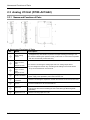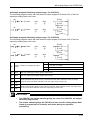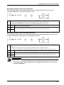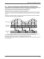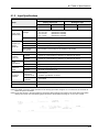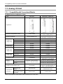
1
Safety Precautions Observe the following notices to ensure personal safety or to prevent accidents. To ensure that you use this product correctly, read this User’s Manual thoroughly before use. Make sure that you fully understand the product and information on safety. This manual uses two safety flags to indicate different levels of danger. WARNING If critical situations that could lead to user’s death or serious injury is assumed by mishandling of the product. -Always take precautions to ensure the overall safety of your system, so that the whole system remains safe in the event of failure of this product or other external factor. -Do not use this product in areas with inflammable gas. It could lead to an explosion. -Exposing this product to excessive heat or open flames could cause damage to the lithium battery or other electronic parts. CAUTION If critical situations that could lead to user’s injury or only property damage is assumed by mishandling of the product. -To prevent excessive exothermic heat or smoke generation, use this product at the values less than the maximum of the characteristics and performance that are assured in these specifications. -Do not dismantle or remodel the product. It could cause excessive exothermic heat or smoke generation. -Do not touch the terminal while turning on electricity. It could lead to an electric shock. -Use the external devices to function the emergency stop and interlock circuit. -Connect the wires or connectors securely. The loose connection could cause excessive exothermic heat or smoke generation. -Do not allow foreign matters such as liquid, flammable materials, metals to go into the inside of the product. It could cause excessive exothermic heat or smoke generation. -Do not undertake construction (such as connection and disconnection) while the power supply is on. It could lead to an electric shock. Copyright / Trademarks -This manual and its contents are copyrighted. -You may not copy this manual, in whole or part, without written consent of Panasonic Industrial Devices SUNX Co., Ltd. -Windows is a registered trademark of Microsoft Corporation in the United States and other countries. -All other company names and product names are trademarks or registered trademarks of their respective owners. PLC_ORG Introduction Thank you for buying a Panasonic product. Before you use the product, please carefully read the installation instructions and the users manual, and understand their contents in detail to use the product properly. Types of Manual • There are different types of users manual for the FP0R series, as listed below. Please refer to a relevant manual for the unit and purpose of your use. • The manuals can be downloaded on our website: http://industrial.panasonic.com/ac/e/dl_center/manual/ Unit name or purpose of use FP0R Control Unit Manual name Manual code FP0R User's Manual ARCT1F475E FPΣ User's Manual ARCT1F333E FP0R Analog I/O Unit User's Manual WUME-FP0RAIO Programming FP-series Programming Manual ARCT1F313E Programming Software FPWIN GR FPWIN GR Operation Guide (Non-free) ARCT1F332E FP0R Expansion I/O Unit FPΣ Control Unit FP0R Analog Input Unit FP0R Analog Output Unit FP0R Analog I/O Unit Table of Contents Table of Contents 1. Unit Functions and Restrictions ....................................... 1-1 1.1 Unit Functions and How They Work ......................................................1-2 1.1.1 Functions of Unit ..................................................................................... 1-2 1.1.2 Unit Type ................................................................................................. 1-2 1.1.3 Restrictions on Units Combination .......................................................... 1-2 2. Names and Functions of Parts ......................................... 2-1 2.1 2.2 2.3 Analog Input Unit (FP0R-AD4/AD8) .......................................................2-2 2.1.1 Names and Functions of Parts ................................................................ 2-2 2.1.2 Setting of Mode Switch............................................................................ 2-3 Analog Output Unit (FP0R-DA4) ............................................................2-4 2.2.1 Names and Functions of Parts ................................................................ 2-4 2.2.2 Setting of Mode Switch............................................................................ 2-5 Analog I/O Unit (FP0R-A21/A42) ...........................................................2-6 2.3.1 Names and Functions of Parts ................................................................ 2-6 2.3.2 Setting of Mode Switch............................................................................ 2-7 3. Wiring ................................................................................. 3-1 3.1 3.2 3.3 ii Analog Input Unit (FP0R-AD4/AD8) .......................................................3-2 3.1.1 Terminal Layout Diagrams ...................................................................... 3-2 3.1.2 Wiring of Analog Input Unit...................................................................... 3-3 Analog Output Unit (FP0R-DA4) ............................................................3-4 3.2.1 Terminal Layout Diagrams ...................................................................... 3-4 3.2.2 Wiring of Analog Output Unit ................................................................... 3-5 Analog I/O Unit (FP0R-A21/A42) ...........................................................3-6 3.3.1 Terminal Layout Diagrams ...................................................................... 3-6 3.3.2 Wiring of Analog I/O Unit ......................................................................... 3-7 Table of Contents 3.4 Common Precautions............................................................................ 3-8 3.4.1 Wiring of Analog I/O Unit ......................................................................... 3-8 3.4.2 Wiring of Power Cable (FP0R-DA4 / FP0R-A21 / FP0R-A42) ................ 3-9 4. Creating Programs ............................................................. 4-1 4.1 I/O Allocation ........................................................................................ 4-2 4.1.1 4.2 4.3 4.4 4.5 I/O Allocation ........................................................................................... 4-2 Analog input unit (FP0R-AD4/AD8) ....................................................... 4-4 4.2.1 Reading of Input Data (Common to 12-bit Mode and 14-bit Mode) ........ 4-4 4.2.2 Setting of Input Range and Averaging Processing (14-bit Mode Only) .. 4-6 Analog Output Unit (FP0R-DA4) ........................................................... 4-8 4.3.1 Writing of Digital Data for Output (12-bit Mode) ...................................... 4-8 4.3.2 Writing of Digital Data for Output (14-bit Mode) .................................... 4-14 4.3.3 Switching of Output Range (14-bit Mode Only) .................................... 4-20 4.3.4 Status Information (12-bit mode)........................................................... 4-22 4.3.5 Status information (14-bit mode) ........................................................... 4-23 Analog I/O Unit (FP0R-A21/A42) ........................................................ 4-24 4.4.1 Reading of Analog Input Values (For A21) ........................................... 4-24 4.4.2 Reading of Analog Input Values (For A42) ........................................... 4-25 4.4.3 Writing of Digital Data for Output (12-bit Mode) .................................... 4-28 4.4.4 Writing of Digital Data for Output (14-bit Mode) .................................... 4-30 4.4.5 Switching of Input Range and Averaging Method (14-bit Mode Only) .. 4-32 4.4.6 Switching of Output Range (14-bit Mode Only) .................................... 4-34 I/O Conversion Characteristics............................................................ 4-36 4.5.1 Input Conversion Characteristics (Voltage Range) ............................... 4-36 4.5.2 Input conversion Characteristics (Current Range) ................................ 4-38 4.5.3 Output conversion Characteristics (Voltage Range) ............................. 4-39 4.5.4 Output conversion Characteristics (Current Range) ............................. 4-41 5. Analog Input Averaging Processing ................................. 5-1 5.1 Types of Averaging Processing ............................................................. 5-2 iii Table of Contents 5.2 5.1.1 Moving Average 10 Times....................................................................... 5-2 5.1.2 Number of Averaging Times (64 times/128 times: 14-bit Mode Only) .... 5-3 Setting of Averaging Processing ............................................................5-4 5.2.1 Enabling Averaging Processing .............................................................. 5-4 6. Specifications .................................................................... 6-1 6.1 6.2 Table of Specifications ..........................................................................6-2 6.1.1 General Specifications ............................................................................ 6-2 6.1.2 Input Specifications ................................................................................. 6-3 6.1.3 Output Specifications .............................................................................. 6-4 Dimension .............................................................................................6-5 7. Compatibility with Conventional Models ......................... 7-1 7.1 7.2 7.3 iv Analog Input Unit ...................................................................................7-2 7.1.1 Compatibility with Conventional Models .................................................. 7-2 7.1.2 Points of Replacement ............................................................................ 7-3 Analog Output Unit ................................................................................7-4 7.2.1 Compatibility with Conventional Models .................................................. 7-4 7.2.2 Points of Replacement ............................................................................ 7-5 Analog I/O Unit ......................................................................................7-6 7.3.1 Compatibility with Conventional Models .................................................. 7-6 7.3.2 Points of Replacement ............................................................................ 7-7 1 Unit Functions and Restrictio ns Unit Functions and Restrictions 1.1 Unit Functions and How They Work 1.1.1 Functions of Unit Attaching these units to FP0R Control Unit enables analog I/O control. • It is selectable from five types of units in accordance with the intended use. Compatibility mode with conventional models is prepared. • The compatibility mode which enables smooth transition from conventional Analog I/O Units (FP0-A80, FP0-A04V, FP0-A04I, FP0-A21) is prepared. 14-bit processing mode is added. • The high-resolution 14-bit mode (1/16000) is added to the both input and output. Also, ranges for each channel can be specified by user programs. 1.1.2 Unit Type Name FP0R Analog Input unit FP0R Analog Output Unit FP0R Analog I/O Unit Specifications Product number 4-ch input AFP0RAD4 8-ch input AFP0RAD8 4-ch output AFP0RDA4 2-ch Input, 1-ch output AFP0RA21 4-ch Input, 2-ch output AFP0RA42 1.1.3 Restrictions on Units Combination Up to three units can be connected with the control unit including other FP0/FP0R Expansion I/O Unit and intelligent unit. 1-2 2 Names and Functions of Parts Names and Functions of Parts 2.1 Analog Input Unit (FP0R-AD4/AD8) 2.1.1 Names and Functions of Parts Names and Functions of Parts No. Name Description ① Mode setting switch Used for selecting the input range, the number of input channels and whether to use the averaging processing or not. Used for selecting the operation mode (12-bit mode or 14-bit mode compatible with the conventional product FP0-A80). ② Input terminal for CH0-CH3 Used for connecting the analog input device. ③ Input terminal for CH4-CH7 Used for connecting the analog input device. ④ Expansion connector Used for connecting the expansion unit with the internal circuit of the Control Unit. ⑤ DIN rail installing groove It can be installed to a 35-mm-wide DIN rail. ⑥ DIN hook The unit can be installed to the DIN rail through one-touch operation. This hook is also used for installing the unit to the Slim Type Mounting Plate (AFP0803). ⑦ Expansion hook Used for securing expansion units. 2-2 2.1 Analog Input Unit (FP0R-AD4/AD8) 2.1.2 Setting of Mode Switch Setting of the mode switch Item Resolution and FP0-A21compatible 12-bit mode input range The number of converted CH Input averaging No. Settings 1 OFF ON OFF ON 2 OFF OFF ON ON FP0-A80compatible 12-bit mode 0 to 5V/0 to 20mA (Note 1) FP0-A80compatible 12-bit mode -10 to +10V Reserved for system (Not settable) 14-bit mode (Note 2) 3 OFF ON OFF ON 4 OFF OFF ON ON 2ch (CH0-CH1) 4ch (CH0-CH3) 6ch (CH0-CH5) 8ch (CH0-CH7) 5 OFF: Averaging Not performed, ON: Averaging Performed (Note 1): When the both switch No.1 and No.2 are OFF, the voltage/current is switched by the connection method. (Note 2): In the 14-bit mode, the input range is set by writing into the operation memory WY with a user program. (Note 3): All the switches are set to OFF at the factory. (Note 4): The switch settings will be valid when the power is turned ON from OFF. The settings will not change if the operation power supply is switched when it is ON. 2-3 Names and Functions of Parts 2.2 Analog Output Unit (FP0R-DA4) 2.2.1 Names and Functions of Parts Names and Functions of Parts No. Name Description ① Mode setting switch Used for selecting the output range and the output method (voltage/current). Used for selecting the operation mode (12-bit mode or 14-bit mode compatible with the conventional product FP0-A04V/A04I). ② Voltage output terminal for CH0-CH3 ③ Current output terminal for CH0-CH3 ④ Power connector 24 V DC is supplied from an external power supply.For connection, use the power supply cable (AFP0581) that comes with the Unit. ⑤ Expansion connector Used for connecting the expansion unit with the internal circuit of the Control Unit. ⑥ DIN rail installing groove It can be installed to a 35-mm-wide DIN rail. ⑦ DIN hook The unit can be installed to the DIN rail through one-touch operation. This hook is also used for installing the unit to the Slim Type Mounting Plate (AFP0803). ⑧ Expansion hook Used for securing expansion units. 2-4 Used for connecting the analog output device. The voltage and current vary according to the settings of the mode switch. They can be selected for each channel. 2.2 Analog Output Unit (FP0R-DA4) 2.2.2 Setting of Mode Switch Setting of the mode switch Item No. Settings Resolution 1 OFF:FP0-A04V/A04I compatible 12-bit mode, ON:14-bit mode (Note 1) 2 CH0 3 CH1 4 CH2 5 CH3 Output switch OFF:Voltage output ON:Current output (Note 2) (Note 1): In the 14-bit mode, the output range is set by writing into the operation memory WY with a user program. (Note 2): For the both FP0-A04V/A04I compatibility 12-bit mode and 14-bit mode, the output can be selected for each channel. (Note 3): All the switches are set to OFF at the factory. (Note 4): The switch settings will be valid when the power is turned ON from OFF. The settings will not change if the operation power supply is switched when it is ON. KEY POINTS • In the FP0-A04V/A04I compatibility 12-bit mode, the voltage output range is -10 to +10 V, and the current output range is 4 to 20 mA. 2-5 Names and Functions of Parts 2.3 Analog I/O Unit (FP0R-A21/A42) 2.3.1 Names and Functions of Parts Names and Functions of Parts No. Name Description ① Mode setting switch Used for selecting the input and output ranges, the output method (voltage/current), and whether to perform the input averaing processing or not. Used for selecting the operation mode (12-bit mode or 14-bit mode compatible with the conventional product FP0-A21). ② I/O terminal Input for CH0CH1 Output for CH0 ③ I/O terminal Input for CH2CH3 Output for CH1 ④ Power connector The supply 24 V DC from an external power supply. For connection, use the power supply cable (AFP0581) that comes with the Unit. ⑤ Expansion connector Used for connecting the expansion unit with the internal circuit of the Control Unit. ⑥ DIN rail installing groove It can be installed to a 35-mm-wide DIN rail. ⑦ DIN hook The unit can be installed to the DIN rail through one-touch operation. This hook is also used for installing the unit to the Slim Type Mounting Plate (AFP0803). ⑧ Expansion hook Used for securing expansion units. 2-6 Used for connecting the analog input device or analog output device. The voltage and current vary according to the settings of the mode switch. They can be selected for each channel. 2.3 Analog I/O Unit (FP0R-A21/A42) 2.3.2 Setting of Mode Switch Setting of the mode switch Item I/O resolution and FP0-A21compatible 12-bit mode input range FP0-A21compatible 12-bit mode output range (Note 3) 14-bit mode output switch (Note 4) Input averaging No. Settings 1 OFF ON OFF ON 2 OFF OFF ON ON FP0-A21compatible 12-bit mode 0 to 5V/0 to 20mA (Note 1) FP0-A21compatible 12-bit mode -10 to +10V Reserved for system (Not settable) 14-bit mode (Note 2) 3 OFF ON OFF ON 4 OFF OFF ON ON FP0-A21compatible 12-bit mode 0 to 20mA Reserved for system (Not settable) FP0-A21compatible 12-bit mode -10 to +10V Reserved for system (Not settable) 3 OFF ON OFF ON 4 OFF OFF ON ON CH0 Voltage output CH1 Voltage output CH0 Current output CH1 Voltage output CH0 Voltage output CH1 Current output CH0 Current output CH1 Current output 5 OFF: Averaging Not performed, ON: Averaging Performed (Note 1): When the both switch No.1 and No.2 are OFF, the input voltage/current is switched by the connection method. (Note 2): In the 14-bit mode, the input and ouput ranges are set by writing into the operation memory WY with a user program. (Note 3): The setting of "FP0-A21 compatibility 12-bit mode output switch" of the switches No.3 and No.4 is valid when the switch No.2 is off. (Note 4): The setting of "14-bit mode output switch" of the switches No.3 and No.4 is valid when the both switch No.1 and No.2 are on. Switching CH1 is available only for A42 type. (Note 5): All the switches are set to OFF at the factory. (Note 6): The switch settings will be valid when the power is turned ON from OFF. The settings will not change if the operation power supply is switched when it is ON. 2-7 Names and Functions of Parts 2-8 3 Wiring Wiring 3.1 Analog Input Unit (FP0R-AD4/AD8) 3.1.1 Terminal Layout Diagrams Appearance Pin No. Name 1 V0 Function CH0 Voltage signal input 2 I0 CH0 Current signal input 3 V1 CH1 Voltage signal input 4 I1 CH1 Current signal input 5 COM 6 V2 CH2 Voltage signal input 7 I2 CH2 Current signal input 8 V3 CH3 Voltage signal input 9 I3 CH3 Current signal input Pin No. Name 1 V4 CH4 Voltage signal input 2 I4 CH4 Current signal input 3 V5 CH5 Voltage signal input 4 I5 CH5 Current signal input 5 COM 6 V6 CH6 Voltage signal input 7 I6 CH6 Current signal input 8 V7 CH7 Voltage signal input 9 I7 CH7 Current signal input Input common Analog input Function Input common Analog input (Note 1): For inputting a current signal, connect the V terminal and I terminal externally. (Note 2):Two COM terminals are connected internally. 3-2 3.1 Analog Input Unit (FP0R-AD4/AD8) 3.1.2 Wiring of Analog Input Unit Voltage input Connect input instrument between V and COM terminal. Current input First, connect both V terminal and I terminal. And then connect input instrument between it and COM terminal. (Note 1): Two COM terminals are connected internally. (Note 2): Two cables or less must be inserted to COM terminal as above (two channel once combined). (Note 3): Recommend using the twisted and shielded communication cables for analog lines and grounding the end of shield. 3-3 Wiring 3.2 Analog Output Unit (FP0R-DA4) 3.2.1 Terminal Layout Diagrams Appearance Pin No. Name 1 V0 CH0 2 COM --- 3 VI CH1 4 COM --- 5 V2 6 COM --- 7 V3 CH3 8 COM 9 NC Pin No. Name Analog output CH2 --- Voltage signal output Output common Voltage signal output Output common Voltage signal output Output common Voltage signal output Output common Unused Function 1 I0 CH0 2 COM --- 3 I1 CH1 4 COM --- 5 I2 6 COM --- 7 I3 CH3 8 COM 9 NC (Note): All COM terminals are connected within the unit. 3-4 Function Analog output CH2 --Unused Current signal output Output common Current signal output Output common Current signal output Output common Current signal output Output common 3.2 Analog Output Unit (FP0R-DA4) 3.2.2 Wiring of Analog Output Unit When the voltage output When current output (Note):All COM terminals of the voltage output terminal block and current output terminal block are connected internally. 3-5 Wiring 3.3 Analog I/O Unit (FP0R-A21/A42) 3.3.1 Terminal Layout Diagrams Appearance Pin No. Name Function 1 IN V0 2 IN I0 3 IN COM 4 IN VI 5 IN CH0 Analog input I1 6 7 OUT V0 8 OUT I0 9 OUT COM Name Current signal input Input common CH1 Voltage signal input CH1 Current signal input Analog output CH0 Voltage signal output CH0 Current signal output --- Output common Function 1 IN 2 IN I0 3 IN COM 4 IN VI 5 IN 6 --- Voltage signal input For shield connection of analog signal cable FG Pin No. CH0 V0 CH2 CH2 Analog input I1 --- Voltage signal input Current signal input Input common CH3 Voltage signal input CH3 Current signal input For shield connection of analog signal cable FG 7 OUT V1 8 OUT I1 9 OUT COM Analog output CH1 Voltage signal output CH1 Current signal output --- Output common (Note 1):For inputting a current signal to the analog input part, connect the V terminal and I terminal externally. (Note 2): All COM terminals are connected within the unit. 3-6 3.3 Analog I/O Unit (FP0R-A21/A42) 3.3.2 Wiring of Analog I/O Unit Analog input Voltage input Connect input instrument between IN/V and IN/COM terminal. Voltage output Connect output instrument between OUT/V and OUT/COM terminal. Current input First,connect both IN/V terminal and IN/I terminal. And then connect input instrument between it and IN/COM terminal. Current output Connect output instrument between OUT/I and OUT/COM terminal. (Note 1):In the above figure, the input (CH0/CH1) and output CH0 are described as representative examples. The input (CH2/CH3) and output CH1 of A42 type also have the same terminal layouts. (Note 2): All COM terminals are connected within the unit. 3-7 Wiring 3.4 Common Precautions 3.4.1 Wiring of Analog I/O Unit Wiring diagram Voltage input Current input Analog device *1 Analog device V V I I COM COM *1: For the current input, short-circuit the V and I terminals. Voltage output Current output V V I I Analog device Analog device COM COM Precautions on Wiring • Use double-core twisted-pair shielded wires. It is recommended to ground the shielding. However, depending on the conditions of the external noise, it may be better not to ground the shielding. • Do not have the analog input wiring close to AC wires, power wires, or load wires. • Do not have the analog output wiring close to AC wires, power wires, or load wires. Compatible cable (twisted wire) Size Nominal cross section area AWG#28-16 0.08 mm2 -1.25 mm2 Special tools Manufacturer Serial number (model number) Phoenix Contact Co. SZS0.4×2.5(1205037) 3-8 3.4 Common Precautions 3.4.2 Wiring of Power Cable (FP0R-DA4 / FP0R-A21 / FP0R-A42) The power needs to be supplied to the analog output unit (FP0R-DA4) and analog I/O unit (FP0R-A21/FP0R-A42) for operation. Precautions on Wiring • It is connected using the cable (Part number:AFP0581) supplied with the unit. • The input voltage range of the power supply for operating the unit is 20.4 to 28.8 VDC. • Use the power supply of SELV (Safety Extra-Low Voltage) and LIM (Limited Energy Circuit). • In order to avoid influence of noise, the function earth terminal must be grounded. 3-9 Wiring 3-10 4 Creating Programs Creating Programs 4.1 I/O Allocation 4.1.1 I/O Allocation • For analog input data and analog output data, input relays (WX) and output relays (WY) are read and written to the control unit. • I/O numbers do not need to be set as I/O allocation is performed automatically. • I/O numbers vary according to installation positions. • The allocated contents vary according to the type of units and mode. For details, refer to the chapters 4.2 to 4.4. 4-2 4.1 I/O Allocation I/O number Type of unit FP0R Analog input unit AFP0RAD4 (Note 1) AFP0RAD8 FP0R Analog output unit AFP0RDA4 FP0R Analog I/O unit AFP0RA21 (Note 3) AFP0RA42 Allocation content Expansion unit 1 Expansion unit 2 Expansion unit 3 Input CH0/CH2/CH4/CH6 WX2 (X20~X2F) WX4 (X40~X4F) WX6 (X60~X6F) Input CH1/CH3/CH5/CH7 WX3 (X30~X3F) WX5 (X50~X5F) WX7 (X70~X7F) Output 14-bit mode range setting WY2 (Y20~Y2F) WY4 (Y40~Y4F) WY6 (Y60~Y6F) Output 14-bit mode range averaging setting WY3 (Y30~Y3F) WY5 (Y50~Y5F) WY7 (Y70~Y7F) WX2 (X20~X2F) WX4 (X40~X4F) WX6 (X60~X6F) WX3 (X30~X3F) WX5 (X50~X5F) WX7 (X70~X7F) Output (Note 2) CH0/CH2 WY2 (Y20~Y2F) WY4 (Y40~Y4F) WY6 (Y60~Y6F) Output (Note 2) CH1/CH3 WY3 (Y30~Y3F) WY5 (Y50~Y5F) WY7 (Y70~Y7F) Input CH0/CH2 WX2 (X20~X2F) WX4 (X40~X4F) WX6 (X60~X6F) Input CH1/CH3 WX3 (X30~X3F) WX5 (X50~X5F) WX7 (X70~X7F) Output (Note 4) CH0 WY2 (Y20~Y2F) WY4 (Y40~Y4F) WY6 (Y60~Y6F) Output (Note 4) CH1 WY3 (Y30~Y3F) WY5 (Y50~Y5F) WY7 (Y70~Y7F) Input Status information (Power ON/OFF, Write state) (Note 1):On AFP0RAD4, data of CH0 to CH3 is handled. (Note 2):It can be also used for switching the output range in the 14-bit mode. (Note 3):On AFP04A21, data of input CH0/CH1 and output CH0 is handled. (Note 4):It can be also used for the input range, averaging setting for input and switching the output range in the 14bit mode. 4-3 Creating Programs 4.2 Analog input unit (FP0R-AD4/AD8) 4.2.1 Reading of Input Data (Common to 12-bit Mode and 14-bit Mode) The analog input unit uses the most significant 2 bits as a flag for switching channels and reads conversion data sequentially. I/O allocation (External input WX) X X X X X X X X X X X X X X X X 3 3 3 3 3 3 3 3 3 3 3 3 3 3 3 3 F E D C B A 9 8 7 6 5 4 3 2 1 0 Conversion data of CH1/CH3/CH5/CH7 (14 bit with sign) A A 1 0 X X X X X X X X X X X X X X X X 2 2 2 2 2 2 2 2 2 2 2 2 2 2 2 2 F E D C B A 9 8 7 6 5 4 3 2 1 0 Conversion data of CH0/CH2/CH4/CH6 (16 bit with sign) Conversion data switch flag A1 A0 WX3 WX2 0 0 CH1 data CH0 data 0 1 CH3 data CH2 data 1 0 CH5 data CH4 data 1 1 CH7 data CH6 data Role of conversion data switching flag • The analog input unit reads the analog input data of a maximum of 8 channels using two memory areas (WX2 and WX3). The most significant two bits are allocated as a conversion data switching flag for distinguishing channels. • Conversion data of even numbered channels can be read as 16-bit data as they are. • As conversion data of odd numbered channels contain the conversion data switching flag of most significant two bits, mask processing needs to be applied to the data with a user program. Plus conversion data should be masked by "00", and minus conversion data should be masked by "11". Create a program in reference to the following programs. (Example):For reading data of CH3 CH3 data 4-4 WX3 Data after masking Description 1 0100 0000 0000 0001 0000 0000 0000 0001 Most significant two bits are masked by "00". -1 0111 1111 1111 1111 1111 1111 1111 1111 Most significant two bits are masked by "11". 4.2 Analog input unit (FP0R-AD4/AD8) Sample program (Analog input: For ranges of -10 V to +10 V and -5 V to +5 V) The following program shows the case that conversion data of the first expansion analog input unit (CH0 to CH7) is read and stored in DT0 to DT7. X3F X3E ① ② [ F0 MV X3D ③ X3D X3F X3E ① ② ③ ③ X3D X3F X3E ① ② ③ ③ X3D X3F X3E ① ② ] ⓑ [ F66 WOR , WX3 , HC000 , DT1 ] ⓒ ③ ③ X3D ③ ⓐ ] ] ⓑ [ F66 WOR , WX3 , HC000 , DT3 ] ⓒ , WX2 , DT4 ⓐ ] [ F65 WAN , WX3 , H3FFF , DT5 ] ⓑ [ F66 WOR , WX3 , HC000 , DT5 ] ⓒ [ F0 MV X3D , WX2 , DT2 [ F65 WAN , WX3 , H3FFF , DT3 [ F0 MV X3D ⓐ ] [ F65 WAN , WX3 , H3FFF , DT1 [ F0 MV X3D , WX2 , DT0 , WX2 , DT6 ⓐ ] [ F65 WAN , WX3 , H3FFF , DT7 ] ⓑ [ F66 WOR , WX3 , HC000 , DT7 ] ⓒ ① X3F ② X3E ③ X3D ⓐ Conversion data of even numbered channels CH0/CH2/CH4/CH6 is transferred as is. ⓑ When the data of odd numbered channels CH1/CH3/CH5/HC7 is positive, the most significant two bits are masked by "00" with F65 WAN (AND) instruction, and the data is stored in DT1/DT3/DT5/DT7. ⓒ When the data of odd numbered channels CH1/CH3/CH5/HC7 is negative, the most significant two bits are masked by "11" with F66 WOR (OR) instruction, and the data is stored in DT1/DT3/DT5/DT7. The channels of conversion data read by turning on/off the conversion data switching flags X3F and X3E are distinguished. The signs of conversion data of read odd numbered channels are distinguished. When plus, OFF. When minus, ON. 4-5 Creating Programs Sample program (For ranges of 0 to 10 V, 0 to 5 V and 0 to 20 mA) The following program shows the case that conversion data of the first expansion analog input unit (CH0 to CH7) is read and stored in DT0 to DT7. X3F X3E ① ② X3F X3E ① ② X3F X3E ① ② [ F0 MV , WX2 , DT0 [ F65 WAN , WX3 , H3FFF , DT1 [ F0 MV , WX2 , DT2 , WX2 , DT4 X3E ① ② [ F0 MV , WX2 , DT6 ] ⓑ ⓐ ] ⓑ ⓐ ] [ F65 WAN , WX3 , H3FFF , DT7 ⓑ ⓐ ] [ F65 WAN , WX3 , H3FFF , DT5 X3F ] ] [ F65 WAN , WX3 , H3FFF , DT3 [ F0 MV ⓐ ] ] ⓑ ① X3F ② X3E ⓐ Conversion data of even numbered channels CH0/CH2/CH4/CH6 is transferred as is. ⓑ When the data of odd numbered channels CH1/CH3/CH5/HC7 is positive, the most significant two bits are masked by "00" with F65 WAN (AND) instruction, and the data is stored in DT1/DT3/DT5/DT7. The channels of conversion data read by turning on/off the conversion data switching flags X3F and X3E are distinguished. 4.2.2 Setting of Input Range and Averaging Processing (14-bit Mode Only) When selecting the 14-bit mode in the analog input unit (FP0R-AD4/AD8), the input range and averaging method can be switched by user programs. They both can be set for each channel. Default settings The default settings are as follows; Input range for all channels: -10 to +10 V, Averaging processing: Moving average processing 10 times (Max. and min. removal). The averaging processing is enabled when the mode switch No. 5 is ON. 4-6 4.2 Analog input unit (FP0R-AD4/AD8) I/O allocation (External output WY) D1 Y Y Y Y Y Y Y Y Y Y Y Y Y Y Y Y 3 3 3 3 3 3 3 3 3 3 3 3 3 3 3 3 F E D C B A 9 8 7 6 5 4 3 2 1 0 Y Y Y Y Y Y Y Y Y Y Y Y Y Y Y Y 2 2 2 2 2 2 2 2 2 2 2 2 2 2 2 2 F E D C B A 9 8 7 6 5 4 3 2 1 0 CH7 CH6 CH5 CH4 CH3 CH2 CH1 CH0 D D D D D D D D D D D D D D D D 1 0 1 0 1 0 1 0 1 0 1 0 1 0 1 0 CH7 CH6 CH5 CH4 CH3 CH2 CH1 CH0 D D D D D D D D D D D D D D D D 1 0 1 0 1 0 1 0 1 0 1 0 1 0 1 0 D0 Averaging (Common to each channel) D1 D0 Range (Common to each channel) 0 0 Moving average 10 times (Max. and min. removal) 0 1 1 1 0 1 No. of averaging times: 64 0 1 - 5V to +5V No. of averaging times: 128 1 0 0 to 10V No averaging 1 1 0 to 5V / 0 to 20mA 0 0 -10V to+10V Sample program (Switching input range) The following program shows the case that the input range of CH0 to CH7 of the first expansion analog input unit is set. R0 ( DF ) [ F0 MV , HFF00 ① , WY2 ② ] ① Input a constant for specifying an input range. Set it according to the I/O allocation on the previous page. In the above sample program, HFF00 is input for setting Y2F-Y28 to 1 and Y27-Y20 to 0. The range for CH4 to CH7 is 0 to 5 V/0 to 20 mA, and that for CH0 to CH3 is -10 V to +10 V. ② WY2 Set it for switching the input range. Sample program (Switching averaging processing method) The following program shows the case that the averaging processing method of CH0 to CH7 of the first expansion analog input unit is set. R0 ( DF ) [ F0 MV , HFF00 ① , WY3 ② ] ① Input a constant for specifying an averanging method. Set it according to the I/O allocation on the previous page. In the above sample program, HFF00 is input for setting Y3F-Y38 to 1 and Y37-Y30 to 0. The method of CH4 to CH7 is no averaging processing, and that of CH0 to CH3 is moving average 10 times. ② WY3 Set it for switching the averaging processing method. 4-7 Creating Programs 4.3 Analog Output Unit (FP0R-DA4) 4.3.1 Writing of Digital Data for Output (12-bit Mode) With the analog output unit, the conversion output is performed by using two bits as the switching flags of output channels and writing data. I/O allocation (12-bit FP0-A04 Compatibility mode) Two bits, the bits C and D, are used as the switching flags. X X X X X X X X X X X X X X X X 3 3 3 3 3 3 3 3 3 3 3 3 3 3 3 3 F E D C B A 9 8 7 6 5 4 3 2 1 0 A A 1 0 X X X X X X X X X X X X X X X X 2 2 2 2 2 2 2 2 2 2 2 2 2 2 2 2 F E D C B A 9 8 7 6 5 4 3 2 1 0 Output data of CH1/CH3 (12bit) A A 1 0 Output data switching flag WY3 Output data of CH0/CH2 (12bit) Output data switching flag A1 A0 A1 A0 WY2 0 0 0 1 D/A conversion: None 0 0 D/A conversion: None CH1data 0 1 CH0 data 1 0 CH3 data 1 0 CH2 data 1 1 D/A conversion: None 1 1 D/A conversion: None Writing conversion data • The analog output unit writes the analog output digital data of a maximum of 4 channels to two memory areas (WY2/WY3) by user programs. Output data switching flags for specifying channels are allocated to the two bits of the memory area (WY2/WY3). • In user programs, channels are specified by setting/resetting the output channel swtiching flag right after setting a digital value in the memory area. • As CH0 and CH2, and CH1 and CH3 use each common memory area, data cannot be written to the unit in the same scan. Write data separated into two scans using scan pulse relay R9012, etc. In the channels which are not allocated to the same memory area, data can be written in the same scan. Example Processing Description When CH0 and CH1 are used Writing CH0 data in WY2 at the time of “n” scan Writing CH1 data in WY3 at the time of “n” scan Data can be written in WY2 and WY3 at the time of “n” scan. When CH0 and CH2 are used Writing CH0 data in WY2 at the time of “n” scan Writing CH2 data in WY2 at the time of “n+1” scan Data can be written in WY2 once in 2 scanning processes (at the time of “n” and “n+1” scan). 4-8 4.3 Analog Output Unit (FP0R-DA4) When data is regarded as an error • Digital data from the control unit is written in the analog output unit. When more than the specified amount of data (-2000 to 2000 for voltage type Unit, 0 to 4000 for current type Unit) is written in the Unit, the Unit regards the data as an error and writes the error flag in WX2. As a result, the D/A conversion is not performed. (For analog output, the previous data remains unchanged. When the correct data is written, the error flag is cleared and D/A conversion is executed.) • Output data and output switching flag are allocated to the same I/O number. Data error can be detected successfully with the flags when the digital input value is within the range of K4096 to K4095. Even when the digital input value is out of the range, however, data conversion may be mistakenly conducted as shown below. To prevent this problem, be sure to set up the program to check the upper and lower limits of the digital value. (Example): When writing K4096 in WY2 K4096= 0001 0000 0000 0000 Analog Output Unit regards Y2D and Y2C as output switching flags: Y2D, Y2C = 01 <- CH0 Data =0000 0000 0000 <- 0 Consequently, the analog value that is equivalent to the digital value “0” is output from CH0. Negative data • When the negative data (minus data) is written, set the output switching flag to two's complement data. When specifying the minus data in the decimal data, the data automatically becomes two's complement data. Then, set the output switching flag to two's complement data in the same way as the plus data. (Example): When writing -1 in CH0 -1=1111 1111 1111 1111 <- Two’s complement Setting the output switching flag: 1101 1111 1111 1111 (Bit C=1, Bit D=0 for CH0) 4-9 Creating Programs Sample program (12-bit mode: For the range of -10 V to +10 V) The following program shows the case that the data of DT0 to DT3 is converted and output to the CH0 to CH3 of the first expansion analog output unit. The range for checking digital values written in the output area is changed. R9012 ① > 1 <= K-2000 , DT0 >= ② [ F0 MV K 2000 , DT0 >1 ③ , DT0 , WY2 ] ④Y2C < SET > ⓐCH0 ⑤ Y2D < RST > R9012 ① > 1 <= K-2000 , DT1 >= ② [ F0 MV K 2000 , DT1 >1 ③ , DT1 , WY3 ] ⑥Y3C < SET > ⓑCH1 ⑦ Y3D < RST > R9012 ① > 1 <= K-2000 , DT2 >= ② [ F0 MV K 2000 , DT2 >1 ③ , DT2 , WY2 ] ④Y2C < RST > ⓒCH2 ⑤ Y2D < SET > R9012 ① 1 > <= K-2000 , DT3 >= >1 ③ ② [ F0 MV K 2000 , DT3 , DT3 , WY3 ] ⑥Y3C < RST > ⑦ Y3D < SET > 4-10 ⓓCH3 4.3 Analog Output Unit (FP0R-DA4) ① R9012 ② Checks whether the lower limit value is within the data range that the unit can convert correctly. ③ Checks whether the upper limit value is within the data range that the unit can convert correctly. ④ Y2C ⑤ Y2D ⑥ Y3C ⑦ Y3D ⓐ It is executed when the scan pulse relay is ON and written data is within the upper and lower limits. Data for CH0 is set in DT0, and CH0 is specified by the output data switching flag. ⓑ It is executed when the scan pulse relay is ON and written data is within the upper and lower limits. Data for CH1 is set in DT1, and CH1 is specified by the output data switching flag. ⓒ It is executed when the scan pulse relay is OFF and written data is within the upper and lower limits. Data for CH2 is set in DT2, and CH2 is specified by the output data switching flag. ⓓ It is executed when the scan pulse relay is OFF and written data is within the upper and lower limits. Data for CH3 is set in DT3, and CH3 is specified by the output data switching flag. Switches the timing of writing data by the scan pulse realy. Output data switching flags for even numbered channels. Channel numbers are specified by the two-bit switching flags right after setting conversion data by the transfer instruction F0 MV. Output data switching flags for odd numbered channels. Channel numbers are specified by the two-bit switching flags right after setting conversion data by the transfer instruction F0 MV. KEY POINTS • In the FP0-A04-compatible 12-bit mode, Y2C, Y2D, Y3C and Y3D are used as the output data switching flags. Note that the allocation is different from that in the 14-bit mode. 4-11 Creating Programs Sample program (12-bit mode: For the range of 4 to 20 mA) The following program shows the case that the data of DT0 to DT3 is converted and output to the CH0 to CH3 of the first expansion analog output unit. The range for checking digital values written in the output area is changed. R9012 ① > 1 <= K 0 , DT0 >= ② [ F0 MV K 4000 , DT0 >1 ③ , DT0 , WY2 ] ④Y2C < SET > ⓐCH0 ⑤ Y2D < RST > R9012 ① > 1 <= K 0 , DT1 >= ② [ F0 MV K 4000 , DT1 >1 ③ , DT1 , WY3 ] ⑥Y3C < SET > ⓑCH1 ⑦ Y3D < RST > R9012 ① > 1 <= K 0 , DT2 >= ② [ F0 MV K 4000 , DT2 >1 ③ , DT2 , WY2 ] ④Y2C < RST > ⓒCH2 ⑤ Y2D < SET > R9012 ① 1 > <= K 0 , DT3 >= ② [ F0 MV K 4000 , DT3 >1 ③ , DT3 , WY3 ] ⑥Y3C < RST > ⑦ Y3D < SET > 4-12 ⓓCH3 4.3 Analog Output Unit (FP0R-DA4) ① R9012 ② Checks whether the lower limit value is within the data range that the unit can convert correctly. ③ Checks whether the upper limit value is within the data range that the unit can convert correctly. ④ Y2C ⑤ Y2D ⑥ Y3C ⑦ Y3D ⓐ It is executed when the scan pulse relay is ON and written data is within the upper and lower limits. Data for CH0 is set in DT0, and CH0 is specified by the output data switching flag. ⓑ It is executed when the scan pulse relay is ON and written data is within the upper and lower limits. Data for CH1 is set in DT1, and CH1 is specified by the output data switching flag. ⓒ It is executed when the scan pulse relay is OFF and written data is within the upper and lower limits. Data for CH2 is set in DT2, and CH2 is specified by the output data switching flag. ⓓ It is executed when the scan pulse relay is OFF and written data is within the upper and lower limits. Data for CH3 is set in DT3, and CH3 is specified by the output data switching flag. Switches the timing of writing data by the scan pulse realy. Output data switching flags for even numbered channels. Channel numbers are specified by the two-bit switching flags right after setting conversion data by the transfer instruction F0 MV. Output data switching flags for odd numbered channels. Channel numbers are specified by the two-bit switching flags right after setting conversion data by the transfer instruction F0 MV. KEY POINTS • In the FP0-A04-compatible 12-bit mode, Y2C, Y2D, Y3C and Y3D are used as the output data switching flags. Note that the allocation is different from that in the 14-bit mode. 4-13 Creating Programs 4.3.2 Writing of Digital Data for Output (14-bit Mode) With the analog output unit, the conversion output is performed by using two bits as the switching flags of output channels and writing data. I/O allocation (14-bit mode) In the 14-bit mode, the most significant two bits are used as the switching flags. They are common to the flags for setting ranges. A1 Y Y Y Y Y Y Y Y Y Y Y Y Y Y Y Y 3 3 3 3 3 3 3 3 3 3 3 3 3 3 3 3 F E D C B A 9 8 7 6 5 4 3 2 1 0 Y Y Y Y Y Y Y Y Y Y Y Y Y Y Y Y 2 2 2 2 2 2 2 2 2 2 2 2 2 2 2 2 F E D C B A 9 8 7 6 5 4 3 2 1 0 A A 1 0 A A 1 0 Output data of CH1/CH3 (14bit) Range setting A0 Item A1 Output data of CH0/CH2 (14bit) Range setting A0 Item 0 0 CH1 output range setting 0 0 CH0 output range setting 0 1 CH1 output data 0 1 CH0 output data 1 0 CH3 output data 1 0 CH2 output data 1 1 CH3 output range setting 1 1 CH2 output range setting Writing data for conversion • The analog output unit writes the analog output digital data of a maximum of 4 channels to two memory areas (WY2/WY3) by user programs. Output data switching flags for specifying channels are allocated to the two bits of the memory area (WY2/WY3). • In user programs, channels are specified by setting/resetting the output channel swtiching flag right after setting a digital value in the memory area. • As CH0 and CH2, and CH1 and CH3 use each common memory area, data cannot be written to the unit in the same scan. Write data separated into two scans using scan pulse relay R9012, etc. In the channels which are not allocated to the same memory area, data can be written in the same scan. Example Processing Description When CH0 and CH1 are used Writing CH0 data in WY2 at the time of “n” scan Writing CH1 data in WY3 at the time of “n” scan Data can be written in WY2 and WY3 at the time of “n” scan. When CH0 and CH2 are used Writing CH0 data in WY2 at the time of “n” scan Writing CH2 data in WY2 at the time of “n+1” scan Data can be written in WY2 once in 2 scanning processes (at the time of “n” and “n+1” scan). 4-14 4.3 Analog Output Unit (FP0R-DA4) When data is regarded as an error • Digital data from the control unit is written in the Analog Output Unit. When more than the specified amount of data (-8000 to 8000 for ± range, 0 to 16000 for + range) is written in the Unit, the Unit regards the data as an error and writes the error flag in WX2. As a result, the D/A conversion is not performed. For analog output, the previous data remains unchanged. When the correct data is written, the error flag is cleared and D/A conversion is executed. • Output data and output switching flag are allocated to the sane I/O number. Data error can be detected successfully with the flags when the digital input value is within the range of 8192 to +8191 for ± range, 0 to 16383 for + range. Even when the digital input value is out of the range, however, data conversion may be mistakenly conducted as shown below. To prevent this problem, be sure to set up the program to check the upper and lower limits of the digital value. (Example): When writing K16384 in WY2 K16384= 0001 0000 0000 0000 Analog Output Unit regards Y2D and Y2C as output switching flags: Y2F, Y2E = 01 <- CH0 Data =00 0000 0000 0000 <- 0 Consequently, the analog value that is equivalent to the digital value “0” is output from CH0. Negative data • When the negative data (minus data) is written, set the output switching flag to two's complement data. When specifying the minus data in the decimal data, the data automatically becomes two's complement data. Then, set the output switching flag to two's complement data in the same way as the plus data. (Example): When writing -1 in CH0 -1=1111 1111 1111 1111 <- Two’s complement Setting the output switching flag: 0111 1111 1111 1111 (Bit F=1, Bit E=0 for CH0) 4-15 Creating Programs Sample program (14-bit mode: For ranges of -10 V to +10 V and -5 V to +5 V) The following program shows the case that the data of DT0 to DT3 is converted and output to the CH0 to CH3 of the first expansion analog output unit. The range for checking digital values written in the output area is changed. R9012 ① > 1 <= K-8000 , DT0 >= >1 ③ ② [ F0 MV K 8000 , DT0 , DT0 ] , WY2 ④Y2E < SET > ⓐCH0 ⑤ Y2F < RST > R9012 ① > 1 <= K-8000 , DT1 >= ② >1 ③ , DT1 [ F0 MV K 8000 , DT1 , WY3 ] ⑥Y3E < SET > ⓑCH1 ⑦ Y3F < RST > R9012 ① > 1 <= K-8000 , DT2 >= ② [ F0 MV K 8000 , DT2 >1 ③ , DT2 , WY2 ] ④Y2E < RST > ⓒCH2 ⑤ Y2F < SET > R9012 ① 1 > <= K-8000 , DT3 >= ② [ F0 MV K 8000 , DT3 >1 ③ , DT3 , WY3 ] ⑥Y3E < RST > ⑦ Y3F < SET > 4-16 ⓓCH3 4.3 Analog Output Unit (FP0R-DA4) ① R9012 ② Checks whether the lower limit value is within the data range that the unit can convert correctly. ③ Checks whether the upper limit value is within the data range that the unit can convert correctly. ④ Y2E ⑤ Y2F ⑥ Y3E ⑦ Y3F ⓐ It is executed when the scan pulse relay is ON and written data is within the upper and lower limits. Data for CH0 is set in DT0, and CH0 is specified by the output data switching flag. ⓑ It is executed when the scan pulse relay is ON and written data is within the upper and lower limits. Data for CH1 is set in DT1, and CH1 is specified by the output data switching flag. ⓒ It is executed when the scan pulse relay is OFF and written data is within the upper and lower limits. Data for CH2 is set in DT2, and CH2 is specified by the output data switching flag. ⓓ It is executed when the scan pulse relay is OFF and written data is within the upper and lower limits. Data for CH3 is set in DT3, and CH3 is specified by the output data switching flag. Switches the timing of writing data by the scan pulse realy. Output data switching flags for even numbered channels. Channel numbers are specified by the two-bit switching flags right after setting conversion data by the transfer instruction F0 MV. Output data switching flags for odd numbered channels. Channel numbers are specified by the two-bit switching flags right after setting conversion data by the transfer instruction F0 MV. KEY POINTS • In the 14-bit mode, Y2E, Y2F, Y3E, and Y3F are used as the output data switching flags. Note that the allocation is different from that in the FP0A04-compatible 12-bit mode. 4-17 Creating Programs Sample program (14-bit mode: For ranges of 0 to 10 V, 0 to 5 V, 0 to 20 mA and 4 to 20 mA) The following program shows the case that the data of DT0 to DT3 is converted and output to the CH0 to CH3 of the first expansion analog output unit. The range for checking digital values written in the output area is changed. R9012 ① > 1 <= K 0 , DT0 >= ② [ F0 MV K16000 , DT0 >1 ③ , DT0 , WY2 ] ④Y2E < SET > ⓐCH0 ⑤ Y2F < RST > R9012 ① > 1 <= K 0 , DT1 >= ② [ F0 MV K16000 , DT1 >1 ③ , DT1 , WY3 ] ⑥Y3E < SET > ⓑCH1 ⑦ Y3F < RST > R9012 ① > 1 <= K 0 , DT2 >= ② [ F0 MV K16000 , DT2 >1 ③ , DT2 , WY2 ] ④Y2E < RST > ⓒCH2 ⑤ Y2F < SET > R9012 ① 1 > <= K 0 , DT3 >= ② [ F0 MV K16000 , DT3 >1 ③ , DT3 , WY3 ] ⑥Y3E < RST > ⑦ Y3F < SET > 4-18 ⓓCH3 4.3 Analog Output Unit (FP0R-DA4) ① R9012 ② Checks whether the lower limit value is within the data range that the unit can convert correctly. ③ Checks whether the upper limit value is within the data range that the unit can convert correctly. ④ Y2E ⑤ Y2F ⑥ Y3E ⑦ Y3F ⓐ It is executed when the scan pulse relay is ON and written data is within the upper and lower limits. Data for CH0 is set in DT0, and CH0 is specified by the output data switching flag. ⓑ It is executed when the scan pulse relay is ON and written data is within the upper and lower limits. Data for CH1 is set in DT1, and CH1 is specified by the output data switching flag. ⓒ It is executed when the scan pulse relay is OFF and written data is within the upper and lower limits. Data for CH2 is set in DT2, and CH2 is specified by the output data switching flag. ⓓ It is executed when the scan pulse relay is OFF and written data is within the upper and lower limits. Data for CH3 is set in DT3, and CH3 is specified by the output data switching flag. Switches the timing of writing data by the scan pulse realy. Output data switching flags for even numbered channels. Channel numbers are specified by the two-bit switching flags right after setting conversion data by the transfer instruction F0 MV. Output data switching flags for odd numbered channels. Channel numbers are specified by the two-bit switching flags right after setting conversion data by the transfer instruction F0 MV. KEY POINTS • In the 14-bit mode, Y2E, Y2F, Y3E, and Y3F are used as the output data switching flags. Note that the allocation is different from that in the FP0A04-compatible 12-bit mode. 4-19 Creating Programs 4.3.3 Switching of Output Range (14-bit Mode Only) When selecting the 14-bit mode in the analog output unit (FP0R-DA4), the output range can be switched by user programs. It can be set for each channel. I/O allocation (External input WY) Y Y Y Y Y Y Y Y Y Y Y Y Y Y Y Y 3 3 3 3 3 3 3 3 3 3 3 3 3 3 3 3 F E D C B A 9 8 7 6 5 4 3 2 1 0 Y Y Y Y Y Y Y Y Y Y Y Y Y Y Y Y 2 2 2 2 2 2 2 2 2 2 2 2 2 2 2 2 F E D C B A 9 8 7 6 5 4 3 2 1 0 A A 1 0 A A 1 0 A1 Output data of CH1/CH3 (14bit) Range setting A0 Item A1 Output data of CH0/CH2 (14bit) Range setting A0 Item 0 0 CH1 output range setting 0 0 CH0 output range setting 0 1 CH1 output data 0 1 CH0 output data 1 0 CH3 output data 1 0 CH2 output data 1 1 CH3 output range setting 1 1 CH2 output range setting Each output range is specified by setting the following constants. Item Description Output range setting Input constants for specifying output ranges in the 14-bit area. H30 -10 to +10V / 0 to 20mA H31 -5 to +5V / 4 to 20mA H32 0 to 10V H33 0 to 5V Default settings The default settings are as follows; Output range for all channels: Voltage output range: -10 to +10 V, Current output range: 0 to 20 mA. 4-20 4.3 Analog Output Unit (FP0R-DA4) Sample program (Switching output range: For CH0/CH1) The following program shows the case that the output ranges of CH0 and CH1 of the first expansion analog input unit is set. R0 ( DF ) [ F0 MV , H30 ① , WY2 ] ② ④ Y2E < RST > ⑤ Y2F < RST > R1 ( DF ) [ F0 MV , H30 ① , WY3 ] ③ ⑥ Y3E < RST > ⑦ Y3F < RST > Sample program (Switching output range: For CH2/CH3) The following program shows the case that the output ranges of CH2 and CH3 of the first expansion analog input unit is set. R2 ( DF ) [ F0 MV , H30 ① , WY2 ] ② ④ Y2E < SET > ⑤ Y2F < SET > R3 ( DF ) [ F0 MV , H30 ① , WY3 ] ③ ⑥ Y3E < SET > ⑦ Y3F < SET > ① Input a constant for specifying an output range. H30 -10 to +10V / 0~20mA H31 -5 to +5V / 4~20mA H32 0 to 10V H33 0 to 5V ② WY2 Set it for switching the output range of CH0 or HC2. ③ WY3 Set it for switching the output range of CH1 or HC3. ④ Y2E ⑤ Y2F ⑤ Y3E ⑦ Y3F Output data switching flags for even numbered channels. When Y2E/Y2F is OFF, the output range of CH0 is set. When Y2E/Y2F is ON, the output range of CH2 is set. Output data switching flags for odd numbered channels. When Y3E/Y3F is OFF, the output range of CH1 is set. When Y3E/Y3F is ON, the output range of CH3 is set. KEY POINTS • For CH0/CH1, the output switching flags are reset. For CH2/CH3, the output switching flags are set. • The output switching flags (bit F/bit E) are also used for setting output data. Create a program not to overwrite each other during an operation processing. 4-21 Creating Programs 4.3.4 Status Information (12-bit mode) With the analog output unit, the following information can be monitored in the external input area WX. Status information I/O No. Description X20 Analog output unit power X21-X23 Used in the system X24 CH0 data writing status X25 CH1 data writing status X26 CH2 data writing status X27 CH3 data writing status X28-X2F Used in the system 0: OFF, 1:ON、 0:Normal, 1:Error (Note 1) An error occurs when data written to the memory area (WY2/WY3) is out of each range, and the data conversion is not performed. The error is cleared when data within the range is written and the conversion is performed. (Note 1): Output data and output CH switch flag are allocated to the same I/O number. Data error can be detected successfully with the flags when the digital input value is within the range of K-4096 to K4095. Even when the digital input value is out of the range, however, data conversion may be mistakenly conducted. To prevent this problem, be sure to set up the program to check the upper and lower limits of the digital value. 4-22 4.3 Analog Output Unit (FP0R-DA4) 4.3.5 Status information (14-bit mode) With the analog output unit, the following information can be monitored in the external input area WX. Status information I/O No. Description X20 Analog output unit power X21-X23 Used in the system X24 CH0 data writing status X25 CH1 data writing status X26 CH2 data writing status X27 CH3 data writing status X28-X2F Used in the system 0:OFF, 1:ON、 0:Normal, 1:Error (Note 1) An error occurs when data written to the memory area (WY2/WY3) is out of each range, and the data conversion is not performed. The error is cleared when data within the range is written and the conversion is performed. X30-X33 CH0 range setting state The state of a specified output range can be monitored. The following constants are stored for each range. H0: -10V to +10V, 0mA to 20mA H1: -5V to +5V,4mA to 20mA H2: 0V to 10V H3: 0V to 5V X34-X37 CH1 range setting state Same as above. X38-X3B CH2 range setting state Same as above. X3C-X3F CH3 range setting state Same as above. (Note 1):As output data and the output switching flag are allocated to the same I/O, a data error is detected correctly only when a digital input value is within (K-8192 to K8191) for the ±range and (K0 to K16383) for the + range. In the case of digital input values exceeding these ranges, data may be converted without an error, so always insert a program which checks the upper and lower limits. (Note 2):In the 14-bit mode, the range setting state of each channel specified in WY2 and WY3 can be confirmed. 4-23 Creating Programs 4.4 Analog I/O Unit (FP0R-A21/A42) 4.4.1 Reading of Analog Input Values (For A21) With the analog input unit A21, data can be read as signed 16-bit data as is. I/O allocation (External input WX) X X X X X X X X X X X X X X X X 3 3 3 3 3 3 3 3 3 3 3 3 3 3 3 3 F E D C B A 9 8 7 6 5 4 3 2 1 0 X X X X X X X X X X X X X X X X 2 2 2 2 2 2 2 2 2 2 2 2 2 2 2 2 F E D C B A 9 8 7 6 5 4 3 2 1 0 Conversion data of CH1 (16 bit with sign) Conversion data of CH0 (16 bit with sign) WX3 WX2 CH1data CH0 data Sample program (FP0R-A21 の場合) The following program shows the case that conversion data of the first expansion analog input unit (FP0R-A21) (CH0 to CH7) is read and stored in DT0 to DT7. R9010 [ F0 MV , WX2 , DT0 [ F0 MV , WX3 , DT1 ⓐ ] ] ⓐ The conversion data of CH0 is stored into DT0. ⓑ The conversion data of CH1 is stored into DT1. 4-24 ⓑ 4.4 Analog I/O Unit (FP0R-A21/A42) 4.4.2 Reading of Analog Input Values (For A42) The analog input unit uses the most significant 2 bits as a flag for switching channels and reads conversion data sequentially. I/O allocation (External input WX) X X X X X X X X X X X X X X X X 3 3 3 3 3 3 3 3 3 3 3 3 3 3 3 3 F E D C B A 9 8 7 6 5 4 3 2 1 0 A A 1 0 Conversion data of CH1/CH3 (14 bit with sign) X X X X X X X X X X X X X X X X 2 2 2 2 2 2 2 2 2 2 2 2 2 2 2 2 F E D C B A 9 8 7 6 5 4 3 2 1 0 Conversion data of CH0/CH2 (16 bit with sign) Conversion data switch flag A1 A0 WX3 WX2 0 0 CH1 data CH0 data 0 1 CH3 data CH2 data Role of conversion data switching flag • The analog I/O unit (FP0R-A42) reads the analog input data of a maximum of 4 channels using two memory areas (WX2 and WX3). The most significant two bits are allocated as a conversion data switching flag for distinguishing channels. • Conversion data of even numbered channels can be read as 16-bit data as they are. • As conversion data of odd numbered channels contain the conversion data switching flag of most significant two bits, mask processing needs to be applied to the data with a user program. Plus conversion data should be masked by "00", and minus conversion data should be masked by "11". Create a program in reference to the following programs. (Example): For reading data of CH3 CH3 data WX3 Data after masking Description 1 0100 0000 0000 0001 0000 0000 0000 0001 Most significant two bits are masked by "00". -1 0111 1111 1111 1111 1111 1111 1111 1111 Most significant two bits are masked by "11". 4-25 Creating Programs Sample program (FP0R-A42: For ranges of -10 V to +10 V and -5 V to +5 V) The following program shows the case that conversion data of the first expansion analog I/O unit (FP0R-A42) (CH0 to CH3) is read and stored in DT0 to DT3. X3E [ F0 MV ① X3D ② X3D ② X3E X3D ② X3D ② ⓐ ] [ F65 WAN , WX3 , H3FFF , DT1 ] ⓑ [ F66 WOR , WX3 , HC000 , DT1 ] ⓒ [ F0 MV ① , WX2 , DT0 , WX2 , DT2 ⓓ ] [ F65 WAN , WX3 , H3FFF , DT3 ] ⓔ [ F66 WOR , WX3 , HC000 , DT3 ] ⓕ ① X3E The channels of conversion data read by turning on/off the conversion data switching flag X3E are distinguished. ② X3D The signs of read conversion data of CH1/CH3 are distinguished. When plus, OFF. When minus, ON. ⓐ The conversion data of CH0 is transferred to DT0. ⓑ When the data of CH1 is positive, the most significant two bits are masked by "00" with F65 WAN (AND) instruction, and the data is stored in DT1. ⓒ When the data of CH1 is negative, the most significant two bits are masked by "11" with F66 WOR (OR) instruction, and the data is stored in DT1. ⓓ The conversion data of CH2 is transferred to DT2. ⓔ When the data of CH3 is positive, the most significant two bits are masked by "00" with F65 WAN (AND) instruction, and the data is stored in DT3. ⓕ When the data of CH3 is negative, the most significant two bits are masked by "11" with F66 WOR (OR) instruction, and the data is stored in DT3. 4-26 4.4 Analog I/O Unit (FP0R-A21/A42) Sample program (FP0R-A42: (For ranges of 0 to 10 V, 0 to 5 V and 0 to 20 mA) X3E [ F0 MV , WX2 , DT0 ⓐ ] ① [ F65 WAN , WX3 , H3FFF , DT1 X3E [ F0 MV , WX2 , DT2 ] ⓒ ] ① [ F65 WAN , WX3 , H3FFF , DT3 ⓑ ] ⓓ The channels of conversion data read by turning on/off the conversion data switching flags X3F and X3E are distinguished. ① X3E ⓐ The conversion data of CH0 is stored into DT0. ⓑ The most significant two bits are masked by "00" with F65 WAN (AND) instruction, and the data is stored in DT1. (Note) ⓒ The conversion data of CH2 is stored into DT2. ⓓ The most significant two bits are masked by "00" with F65 WAN (AND) instruction, and the data is stored in DT3. (Note):In the case of data of CH1, it can be replaced with the transfer instruction F0 MV as the conversion data switching flag is "00". 4-27 Creating Programs 4.4.3 Writing of Digital Data for Output (12-bit Mode) The analog I/O unit (FP0R-A42/A21) writes data for conversion as the output switching flags are not contained in the 12-bit mode. I/O allocation (12-bit mode) WY3 WY2 CH1 data CH0 data Writing data for conversion • The analog I/O unit writes the analog output digital data of a maximum of 2 channels to two memory areas (WY2/WY3) by user programs. • Always insert a program which checks the upper and lower limits to make written digital values be within the allowable data ranges referring the programs described on the following pages. Mode Range setting Lower limit Upper limit ± range -2000 2000 + range 0 4000 12-bit mode Sample program (12-bit mode: -10V to +10V range) The following program shows the case that the data of DT0 to DT1 is converted and output to the CH0 to CH1 of the first expansion analog I/O unit (FP0R-A42/A21). R9010 ① > 1 <= K-2000 , DT0 ② [ F0 MV ① 1 > <= , DT0 K-2000 , DT1 >1 , DT1 ⓐCH0 ] ⑤ >= K 2000 , DT1 >1 ③ ④ 4-28 , WY2 ② [ F0 MV K 2000 , DT0 ③ ④ R9010 >= , WY3 ⑤ ] ⓑCH1 4.4 Analog I/O Unit (FP0R-A21/A42) Sample program (12-bit mode: 0 to 20mA range) R9010 ① > 1 R9010 ① 1 > <= K 0 , DT0 >= ② [ F0 MV <= K >1 ③ , DT0 , WY2 ④ ⑤ 0 , DT1 >= ② [ F0 MV K 4000 , DT0 K 4000 , DT1 >1 ③ , DT1 ④ , WY3 ⓐCH0 ] ] ⓑCH1 ⑤ ① R9010 ② Checks whether the lower limit value is within the data range that the unit can convert correctly. ③ Checks whether the upper limit value is within the data range that the unit can convert correctly. ⓐ It is executed when the execution condition is ON and written data is within the upper and lower limits. Data for CH0 is set in DT0, and CH0 is specified by the output data switching flag. ⓑ It is executed when the execution condition is ON and written data is within the upper and lower limits. Data for CH1 is set in DT1, and CH1 is specified by the output data switching flag. Always ON relay 4-29 Creating Programs 4.4.4 Writing of Digital Data for Output (14-bit Mode) With the analog I/O unit (FP0R-A42/A21), the conversion output is performed by using two bits as the switching flags of output channels and writing data. I/O allocation (14-bit mode) In the 14-bit mode, the most significant two bits are used as the switching flags. They are common to the flags for setting ranges. Y Y Y Y Y Y Y Y Y Y Y Y Y Y Y Y 3 3 3 3 3 3 3 3 3 3 3 3 3 3 3 3 F E D C B A 9 8 7 6 5 4 3 2 1 0 A A 1 0 A1 Y Y Y Y Y Y Y Y Y Y Y Y Y Y Y Y 2 2 2 2 2 2 2 2 2 2 2 2 2 2 2 2 F E D C B A 9 8 7 6 5 4 3 2 1 0 Output data of CH1 (14bit) Input average setting: CH0-CH3 CH1 output range setting A0 Item A A 1 0 A1 Output data of CH0 (14bit) Input average setting: CH0-CH3 CH0 output range setting A0 Item 0 0 CH1 output data setting 0 0 CH0 output data setting 0 1 Input average setting 0 1 Input range setting 1 0 CH1 output range setting 1 0 CH0 output range setting 1 1 CH1 output data setting 1 1 CH0 output data setting Writing data for conversion • The analog I/O unit writes the analog output digital data of a maximum of 2 channels to two memory areas (WY2/WY3) by user programs. • Protect output switching flags from being overwritten by a subsequent program after writing data. Output data becomes invalid. • Always insert a program which checks the upper and lower limits to make written digital values be within the allowable data ranges referring the programs described on the following pages. Mode 14-bit mode • 4-30 Range setting Lower limit Upper limit ±range -8000 8000 +range 0 16000 For the analog I/O unit (FP0R-A21/A42), the data setting becomes valid when the output switching flags (Y2F, Y2E) or (Y3F, Y3E) are (0, 0) or (1, 1). When written digital values are within the range in the above table, it is not necessary to add programs for setting or setting the output switching flags after data transmission like the following programs because the output switching flags (Y2F, Y2E) or (Y3F, Y3E) are always (0, 0) or (1, 1). 4.4 Analog I/O Unit (FP0R-A21/A42) Sample program (14-bit mode: For ranges of -10 V to +10 V and -5 V to +5 V) The following program shows the case that the data of DT0 to DT1 is converted and output to the CH0 to CH1 of the first expansion analog I/O unit (FP0R-A42/A21). The range for checking digital values written in the output area is changed. R9010 ① > 1 <= K-8000 , DT0 ② [ F0 MV ① > 1 <= , DT0 K-8000 , DT1 , WY2 >1 >= K 8000 , DT1 >1 ③ , DT1 ④ ⓐCH0 ] ⑤ ② [ F0 MV K 8000 , DT0 ③ ④ R9010 >= , WY3 ⓑCH1 ] ⑤ Sample program (14-bit mode: (For ranges of 0 to 10 V, 0 to 5 V, 0 to 20 mA and 4 to 20 mA) R9010 ① > 1 R9010 ① 1 > <= K 0 , DT0 >= ② [ F0 MV <= K >1 ③ , DT0 , WY2 ④ ⑤ 0 , DT1 >= ② [ F0 MV K16000 , DT0 K16000 , DT1 >1 ③ , DT1 ④ , WY3 ⓐCH0 ] ] ⓑCH1 ⑤ ① R9010 ② Checks whether the lower limit value is within the data range that the unit can convert correctly. ③ Checks whether the upper limit value is within the data range that the unit can convert correctly. ⓐ It is executed when the execution condition is ON and written data is within the upper and lower limits. Data for CH0 is set in DT0, and CH0 is specified by the output data switching flag. ⓑ It is executed when the execution condition is ON and written data is within the upper and lower limits. Data for CH1 is set in DT1, and CH1 is specified by the output data switching flag. Always ON relay 4-31 Creating Programs 4.4.5 Switching of Input Range and Averaging Method (14-bit Mode Only) When selecting the 14-bit mode in the analog I/O unit (FP0R-A21/A42), the input range or averaging method for each channel can be set by user programs. I/O allocation (External output WY) Y Y Y Y Y Y Y Y Y Y Y Y Y Y Y Y 3 3 3 3 3 3 3 3 3 3 3 3 3 3 3 3 F E D C B A 9 8 7 6 5 4 3 2 1 0 A A 1 0 A1 Y Y Y Y Y Y Y Y Y Y Y Y Y Y Y Y 2 2 2 2 2 2 2 2 2 2 2 2 2 2 2 2 F E D C B A 9 8 7 6 5 4 3 2 1 0 Output data of CH1 (14bit) Input average setting: CH0-CH3 CH1 output range setting A0 Item A A 1 0 A1 Output data of CH0 (14bit) Input average setting: CH0-CH3 CH0 output range setting A0 Item 0 0 CH1 output data setting 0 0 CH0 output data setting 0 1 Input average setting 0 1 Input range setting 1 0 CH1 output range setting 1 0 CH0 output range setting 1 1 CH1 output data setting 1 1 CH0 output data setting Set the contents allocated to CH0 to CH3 for the input averaging processing and input range by replacing the following 8-bit data with Hex data. Y Y Y Y Y Y Y Y Y Y Y Y Y Y Y Y 3 3 3 3 3 3 3 3 3 3 3 3 3 3 3 3 F E D C B A 9 8 7 6 5 4 3 2 1 0 A A 1 0 D1 Specify 0 CH3 CH2 CH1 CH0 D D D D D D D D 1 0 1 0 1 0 1 0 D0 Averaging (Common to each channel) 0 0 0 1 1 1 0 1 Moving average 10 times (Max. and min. removal) No. of averaging times: 64 No. of averaging times: 128 No averaging Y Y Y Y Y Y Y Y Y Y Y Y Y Y Y Y 2 2 2 2 2 2 2 2 2 2 2 2 2 2 2 2 F E D C B A 9 8 7 6 5 4 3 2 1 0 A A 1 0 D1 Specify 0 CH3 CH2 CH1 CH0 D D D D D D D D 1 0 1 0 1 0 1 0 D0 Range (Common to each channel) 0 0 -10V to +10V 0 1 1 1 0 1 -5V to +5V 0 to 10V 0 to 5V / 0 to 20mA Default settings The default settings are as follows; Input range for all channels: -10 to +10 V, Averaing processing: Moving average processing 10 times (Max. and min. removal). The averaging processing is enabled when the mode switch No. 5 is ON. 4-32 4.4 Analog I/O Unit (FP0R-A21/A42) Sample program (Input range switching) The following program shows the case that the input range of CH0 to CH3 of the first expansion analog I/O unit (FP0R-A42/A21) is set. R0 ( DF ) [ F0 MV , HF0 ① , WY2 ② ] Y2E < SET > Y2F < RST > ① Input a constant for specifying an input range. Set it according to the I/O allocation on the previous page. In the above sample program, HF0 is input for setting Y27-Y24 to 1 and Y23-Y20 to 0. The range for CH3/CH2 is 0 to 5 V/0 to 20 mA, and that for CH1/CH0 is -10 V to +10 V. ② WY2 ③ Y2E ④ Y2F Set it for switching the input range. Data switching flags. When Y2E is ON and Y2F is OFF, the input range is set. Sample program (Input averaging switching) The following program shows the case that the averaging processing method of CH0 to CH3 of the first expansion analog I/O unit (FP0R-A42/A21) is set. R0 ( DF ) [ F0 MV , HF0 ① , WY3 ② ] Y3E < SET > Y3F < RST > ① Input a constant for specifying an averanging method. Set it according to the I/O allocation on the previous page. In the above sample program, HF0 is input for setting Y37-Y34 to 1 and Y33-Y30 to 0. The method of CH3/CH2 is no averaging processing, and that of CH1/CH0 is moving average 10 times. ② WY3 ③ Y3E ④ Y3F Set it for switching the averaging processing method. Data switching flags. When Y3E is ON and Y3F is OFF, the averaging method of input is set. KEY POINTS • The input range setting and the input averaging method for four channels are set collectively. 4-33 Creating Programs 4.4.6 Switching of Output Range (14-bit Mode Only) When selecting the 14-bit mode in the analog I/O unit (FP0R-A21/A42), the output range can be switched by user programs. It can be set for each channel. I/O allocation (External output WY) Y Y Y Y Y Y Y Y Y Y Y Y Y Y Y Y 3 3 3 3 3 3 3 3 3 3 3 3 3 3 3 3 F E D C B A 9 8 7 6 5 4 3 2 1 0 A A 1 0 A1 Y Y Y Y Y Y Y Y Y Y Y Y Y Y Y Y 2 2 2 2 2 2 2 2 2 2 2 2 2 2 2 2 F E D C B A 9 8 7 6 5 4 3 2 1 0 Output data of CH1 (14bit) Input average setting: CH0-CH3 CH1 output range setting A0 Item A A 1 0 A1 Output data of CH0 (14bit) Input average setting: CH0-CH3 CH0 output range setting A0 Item 0 0 CH1 output data setting 0 0 CH0 output data setting 0 1 Input a average setting 0 1 Input range setting 1 0 CH1 output range setting 1 0 CH0 output range setting 1 1 CH1 output data setting 1 1 CH0 output data setting Each output range is specified by setting the following constants. Item Description Input constants for specifying output ranges in the 14-bit area. H30 -10 to +10V / 0 to 20mA Output range setting H31 H32 H33 -5 to +5V / 4 to 20mA 0 to 10V 0 to 5V Default settings The default settings are as follows; Output range for all channels: Voltage output range: -10 to +10 V, Current output range: 0 to 20 mA. KEY POINTS • 4-34 The output ranges are set for two channels separately. 4.4 Analog I/O Unit (FP0R-A21/A42) Sample program (Output range switching) The following program shows the case that the input range of CH0 and CH1 of the first expansion analog I/O unit (FP0R-A21/A42) is set. R0 R0 ① ( DF ) ( DF ) [ F0 MV [ F0 MV , H30 ① , H30 ① Input a constant for specifying an output range. , WY2 ② , WY3 ③ ] Y2E < RST > Y2F < SET > ] Y3E < RST > Y3F < SET > H30 -10 to +10V / 0 to 20mA H31 -5 to +5V / 4 to 20mA H32 0 to 10V H33 0 to 5V ② WY2 Set it for switching the output range of CH0. ③ WY3 Set it for switching the output range of CH1. ④ Y2E ⑤ Y2F ⑤ Y3E ⑦ Y3F Output data switching flag for CH0. When Y2E is OFF and Y2F is ON, the output range of CH0 is set. Output data switching flag for CH1. When Y3E is OFF and Y3F is ON, the output range of CH1 is set. 4-35 Creating Programs 4.5 I/O Conversion Characteristics 4.5.1 Input Conversion Characteristics (Voltage Range) -10V to +10V DC input Conversion characteristic Correspondence table of A/D Conversion values Input voltage (V) -10.0 -5.0 0 5.0 10.0 Digital value 12-bit 14-bit -2000 -8000 -1000 -4000 0 0 1000 4000 2000 8000 If the input value is out of the range Input voltage (V) Digital value 12-bit 14-bit -10V or less -2000 -8000 10V or more 2000 8000 (Note 1):A digital conversion value equivalent to the analog input value of approx. 2 V is shown for the channels to which no input is connected. -5V to +5V DC input (14-bit mode only) Conversion characteristic Correspondence table of A/D Conversion values Input voltage (V) -5.0 -2.5 0 2.5 5.0 Digital value 14-bit -8000 -4000 0 4000 8000 If the input value is out of the range Input voltage (V) Digital value 14-bit -5V or less -8000 5V or more 8000 (Note 1):A digital conversion value equivalent to the analog input value of approx. 2 V is shown for the channels to which no input is connected. 4-36 4.5 I/O Conversion Characteristics 0V to 10V DC input (14-bit mode only) Conversion characteristic Correspondence table of A/D Conversion values Digital value 14-bit 0 4000 8000 12000 16000 Input voltage (V) 0.0 2.5 5.0 7.5 10.0 Processing if the range is exceeded Digital value Input voltage (V) 14-bit 0V or less (including negative value) 0 10V or more 16000 (Note 1):A digital conversion value equivalent to the analog input value of approx. 2 V is shown for the channels to which no input is connected. 0V to 5V DC input Conversion characteristic Correspondence table of A/D Conversion values Input voltage (V) 0.0 1.25 2.5 3.75 5.0 Digital value 12-bit 0 1000 2000 3000 4000 14-bit 0 4000 8000 12000 16000 Processing if the range is exceeded Input voltage (V) Digital value 12-bit 14-bit 0V or less (including negative value) 0 0 5V or more 4000 16000 (Note 1):A digital conversion value equivalent to the analog input value of approx. 2 V is shown for the channels to which no input is connected. 4-37 Creating Programs 4.5.2 Input conversion Characteristics (Current Range) 0mA to 20mA DC input Conversion characteristic Correspondence table of A/D Conversion values Input current (mA) 0.0 5.0 10.0 15.0 20.0 Digital value 12-bit 0 1000 2000 3000 4000 14-bit 0 4000 8000 12000 16000 Processing if the range is exceeded Input current (mA) 4-38 Digital value 12-bit 14-bit 0mA or less(including negative value) 0 0 20mA or more 4000 16000 4.5 I/O Conversion Characteristics 4.5.3 Output conversion Characteristics (Voltage Range) -10V to 10V DC output Conversion characteristic Correspondence table of D/A Conversion values Digital value 12-bit -2000 -1000 0 1000 2000 14-bit -8000 -4000 0 4000 8000 Output voltage (V) -10.0 -5.0 0.0 5.0 10.0 Processing if the range is exceeded Digital input value -2001 or less -8001 or less 2001 or more 8001 or more Output voltage (V) Refer to the following notes. -5V to 5V DC output (14-bit mode only) Conversion characteristic Correspondence table of D/A Conversion values Digital value 14-bit -8000 -4000 0 4000 8000 Output voltage (V) -5.0 -2.5 0.0 2.5 5.0 Processing if the range is exceeded Digital input value -8001 or less 8001 or more Output voltage (V) Refer to the following notes. KEY POINTS • Mode 12-bit mode 14-bit mode The following operations are performed when a value exceeding the allowable range is written. Always insert a program for checking the upper and lower limits right before a program for writing data. Data range Description -2049 or less 2048 or more The bits D and C of a written value may be regarded as channel switching flags and converted to an unintended value and output. -2048 to -2001 2001 to 2047 The value does not change and the previous value is held. -8193 or less 8192 or more The bits F and E of a written value may be regarded as channel switching flags and converted to an unintended value and output. -8192 to -8001 8001 to 8191 The value does not change and the previous value is held. 4-39 Creating Programs 0V to 10V DC output (14-bit mode only) Conversion characteristic Correspondence table of D/A Conversion values Digital value 14-bit 0 4000 8000 12000 16000 Output voltage (V) 0.0 2.5 5.0 7.5 10.0 Processing if the range is exceeded Digital input value Including negative value 16001 or more Output voltage (V) Refer to the following notes. 0V to 5V DC output (14-bit mode only) Conversion characteristic Correspondence table of D/A Conversion values Digital value 14-bit 0 4000 8000 12000 160000 Output voltage (V) 0.0 1.25 2.5 3.75 5.0 Processing if the range is exceeded Digital input value Including negative value 16001 or more Output voltage (V) Refer to the following notes. KEY POINTS • Mode 14-bit mode 4-40 The following operations are performed when a value exceeding the allowable range is written. Always insert a program for checking the upper and lower limits right before a program for writing data. Data range Description -1 or less 16384 or more The bits F and E of a written value may be regarded as channel switching flags and converted to an unintended value and output. --- 16001 to 16383 The value does not change and the previous value is held. 4.5 I/O Conversion Characteristics 4.5.4 Output conversion Characteristics (Current Range) 0mA to 20mA output Conversion characteristic Correspondence table of D/A Conversion values Digital value 12-bit 14-bit 0 1000 2000 3000 4000 0 4000 8000 12000 16000 Output current (mA) 0.0 5.0 10.0 15.0 20.0 Processing if the range is exceeded Digital value 12-bit 14-bit Including negative value Including negative value 4001 or more 16001 or more Output current (mA) Refer to the notes on the next page. (Note):For the 12-bit mode, the values for FP0R-A21/A42 are shown. For FP0R-DA4 (12-bit mode), the range is 4 mA to 20 mA.。 4mA to 20mA output Conversion characteristic Correspondence table of D/A Conversion values Digital value 12-bit 14-bit 0 1000 2000 3000 4000 0 4000 8000 12000 16000 Output current (mA) 4.0 8.0 12.0 16.0 20.0 Processing if the range is exceeded Digital value 12-bit 14-bit Including negative value Including negative value 4001 or more 16001 or more Output current (mA) Refer to the notes on the next page. (Note):For the 12-bit mode, the values for FP0R-DA4 are shown. For FP0R-A21/A42 (12-bit mode), the range is 0 mA to 20 mA. 4-41 Creating Programs KEY POINTS • Mode 12-bit mode 14-bit mode 4-42 The following operations are performed when a value exceeding the allowable range is written. Always insert a program for checking the upper and lower limits right before a program for writing data. Data range Description -4097 or less 4096 or more The bits D and C of a written value may be regarded as channel switching flags and converted to an unintended value and output. -4096 to -1 4001 to 4095 The value does not change and the previous value is held. -1 or less 16384 or more The bits F and E of a written value may be regarded as channel switching flags and converted to an unintended value and output. --- 16001 to 16383 The value does not change and the previous value is held. 5 Analog Input Averaging Processing Analog Input Averaging Processing 5.1 Types of Averaging Processing 5.1.1 Moving Average 10 Times When the averaging function is set to on, the internal processing of the analog unit is as shown in the diagram below Moving Average Processing • Averages and stores converted values obtained by sampling. • Calculates the average of data for past eight times excluding the maximum and minimum values from the latest data, and stores it in the external input area (WX). If a fraction results from the calculation, it is rounded off. Operation item Timing chart Analog input value Reading time Internal processing for ch0 Digital input value (Note):The above figure shows the processing when the number of input channels is two. 5-2 5.1 Types of Averaging Processing 5.1.2 Number of Averaging Times (64 times/128 times: 14-bit Mode Only) Only when the 14-bit mode is selected, the number of averaging times is selectable. Processing when selecting the number of averaging times • Averages and stores converted values obtained by sampling. • When the number of obtained analog input data reaches the specified number of averaging times (64 or 128 times), performs the average processing and stores the result as a digital value. • Stores the first obtained data in the external input area (WX) when the number of obtained data is less than the number of averaging times. a b c d e f g Analog signal h i j k l m n o p q r Analog input processing Average of a to e Average of f to j Average of k to o Analog input data (Note):To make the explanation simple, the above figure shows the processing which averages data by five times. In the actual processing, calculation is carried out with the average of data for 64 times or 128 times. Setting method of the number of averaging times processing The number of averaging times can be changed by being written to the output relay area (WY) in a user program. 5-3 Analog Input Averaging Processing 5.2 Setting of Averaging Processing 5.2.1 Enabling Averaging Processing The averaging processing can be set by the following methods. 12-bit FP0-A80 compatibility mode / FP0-A21 compatibility mode The averaging processing is enabled only when the mode switch No.5 of the unit is ON. • The averaging method of all channels is the moving average 10 times (Max. and min. removal). 14-bit mode • The averaging processing is enabled only when the mode switch No.5 of the unit is ON. • The default is the moving average 10 times (Max. and min. removal). • It is possible to specify the averaging method (Moving average 10 times / No. of averaging times: 64 / No. of averaging times: 128 / No averaging) by a user program for each channel. REFERENCE 5-4 • For details of the setting method of the mode switch, refer to the chapter 2 “Names and Functions of Parts“. • For details of the programming method for the analog input unit (FP0RAD4/AD8), refer to “4.2.2 Setting of Input Range and Averaging Processing (14-bit Mode Only)“. • For details of the programming method for the analog I/O unit (FP0RA21/A42), refer to PAGEREF“4.4.5 Switching of Input Range and Averaging Method (14-bit Mode Only)“. 6 Specifications Specifications 6.1 Table of Specifications 6.1.1 General Specifications Specifications Item Description Rated operating voltage 24 V DC Operating voltage range 20.4 to 28.8 V DC (Unit input voltage) Rated current consumption AFP0RDA4:180 mA or less AFP0RA21: 80 mA or less AFP0RA42:120 mA or less Allowable instantaneous power-off time 10ms Current consumption increase of control unit AFP0RAD4/ AFP0RAD8 AFP0RDA4 AFP0RA21/ AFP0RA42 Ambient temperature 0°C to +55°C Storage temperature -40°C to +70°C Ambient humidity 10 to 95%RH (at 25°C non condensing) Storage humidity 10 to 95%RH (at 25°C non condensing) Breakdown voltage (Note 1) Insulation resistance :20 mA or less :10 mA or less :10 mA or less Between I/O terminal and control unit power supply terminal / ground terminal <AFP0RA21/AFP0RA42> Between analog input terminal and analog output terminal Between I/O terminal and control unit power supply terminal / ground terminal <AFP0RA21/AFP0RA42> Between analog input terminal and analog output terminal 500 V AC for 1 minute Min. 100 MΩ (measured with a 500V DC megger) Vibration resistance Based on JIS B 3502 and IEC 61131-2: 5 to 8.4 Hz, half amplitude 3.5 mm 8.4 to 150 Hz, constant acceleration 9.8 m/s2 X, Y and Z axes, 10 sweeps (1 octave/mm) Shock resistance Based on JIS B 3502 and IEC 61131-2 147 m/s2 or more, X, Y and Z axes, 3 times Noise immunity 1000V [P-P] with pulse widths 50 ns, 1μs (using noise simulator) (Applied to the power supply part of the control unit) Operating condition Must be free from corrosive gases and excessive dust. EU Directive applicable standard EMC Directive: EN 61131-2 Overvoltage category Category II Pollution level Pollution level 2 Weight AFP0RAD4/ AFP0RA21 AFP0RAD8/ AFP0RDA4/ AFP0RA42 (Note 1):Cutoff current: 5 mA (Factory default setting) 6-2 :Approx. 75 g :Approx. 85 g 6.1 Table of Specifications 6.1.2 Input Specifications Description Item Analog input unit AFP0RAD4 Number of channels Input range (Resolution) Digital input range (Note 2) 4 ch Analog I/O unit AFP0RAD8 AFP0RA21 AFP0RA42 8 ch 2 ch 4 ch Voltage -10 to 10 V DC -5 to 5 V DC 0 to 10 V DC 0 to 5 V DC (Resolution:1/16,000) (Note 1) (Resolution:1/16,000) (Resolution:1/16,000) (Resolution:1/16,000) Current 0 to 20 mA (Resolution:1/16,000) (Note1) -10 to 10 V DC K -2000 to K2000 (12-bit mode)/ K-8000 to K8000 (14-bit mode) -5 to 5 V DC K-8000 to K8000 (14-bit mode only) 0 to 10 V DC K0 to K16000 (14-bit mode only) 0 to 5 V DC 0 to 20 mA K0 to K4000 (14-bit mode)/ K0 to K16000 (14-bit mode) Conversion speed 2 ms / All channels (Note 3) Voltage ±0.2%F.S. or less (at 25°C) ±0.4%F.S. or less (at 0 to +55°C) Current ±0.3%F.S. or less (at 25°C) ±0.6%F.S. or less (at 0 to +55°C) Input impedance Voltage Approx.1 MΩ Current Approx.250 Ω Absolute maximum input Voltage -15 to 15 V (Voltage input) Current -30 to 30 mA (Current input) Between output terminal to internal circuit Photocoupler Insulation-type DC/DC converter Between the channels Uninsulated Overall precision Insulation method FP0 Compatibility Switched to the 12-bit operation by the dip switch. External connection method Connection terminal block connection (Note 1):The resolution in the 12-bit mode is 1/4,000. (Note 2):A digital conversion value equivalent to the analog input value of approx. 2 V is shown for the channels to which no input is connected. (Note 3):The time shown in the figure below is required to reflect analog input values in the input device area (WX) read by the control unit. The following figure shows the values when the range of -10 to +10 V is used. 6-3 Specifications 6.1.3 Output Specifications Description Item Analog output unit Number of outputs Output range (Resolution Digital output range AFP0RDA4 AFP0RA21 AFP0RA42 4 ch 1 ch 2 ch Voltage -10 to 10 V DC -5 to 5 V DC 0 to 10 V DC 0 to 5 V DC (Resolution:1/16,000) (Note 1) (Resolution:1/16,000) (Resolution:1/16,000) (Resolution:1/16,000) Current 0 to 20 mA 4 to 20 mA (Resolution:1/16,000) (Note1) (Resolution:1/16,000) (Note1) -10 to 10 V DC K-2000 to K2000 (12-bit mode)/ K-8000 to K8000 (14-bit mode) -5 to 5 V DC K-8000 to K8000 (14-bit mode only) 0 to 10 V DC 0 to 5 V DC K0 to K16000 (14-bit mode only) 0 to 20 mA 4 to 20 mA K0 to K4000 (12-bit mode)/ K0 ~ K16000 (14-bit mode) (Note1) Conversion speed Overall precision 500 µs / All channels (Note 2) Voltage ±0.2%F.S. or less (at 25°C) ±0.4%F.S. or less (at 0 to +55°C) Current ±0.3%F.S. or less (at 25°C) ±0.6%F.S. or less (at 0 to +55°C) Output impedance 0.5 Ω or less (Voltage output) Maximum outputcurrent ±10 mA (Voltage output) Allowable outputload resistance 600 Ω or less (Current output) Insulation method Analog I/O unit Between input terminal to internal circuit Photocoupler Insulation-type DC/DC converter Between the channels Uninsulated External connection method Connection terminal block connection (Note 1):The resolution in the 12-bit mode is 1/4,000. Also, the output current range in the 12-bit mode is 4 to 20 mA for AFP0RDA4, and 0 to 20 mA for AFP0RA21/AFP0RA42. (Note 2): The time shown in the figure below is required to reflect the values in the output device area (WY) of the control unit as analog output values. The following figure shows the values when the range of -10 to +10V is used. Precautions on the characteristics of analog output When the power to the control unit turns on or off, voltage (equivalent to 2 V) may be output for approx. 2 ms from the output terminal. If it will be a problem on your system, take necessary measures externally to avoid the transitional condition, e.g. turning on PLC before external devices or turning off external devices before PLC. 6-4 6.2 Dimension 6.2 Dimension FP0R-AD4 / FP0R-A21 (Note): FP0R-AD4 has no power supply connector. FP0R-AD8 / FP0R-DA4 / FP0R-A42 (Note): FP0R-AD8 has no power supply connector. 6-5 Specifications 6-6 7 Compatibility with Conventional Models Compatibility with Conventional Models 7.1 Analog Input Unit 7.1.1 Compatibility with Conventional Models Specification Comparison Chart Item FP0-A80 FP0RAD4 / FP0RAD8 12-bit (1/4000) 12-bit (1/4000) 14-bit (1/16000) (Note 1) 8 ch 4 ch or 8 ch (Each model) Appearance Resolution and Operation mode Number of channels Analog input voltage range Analog input current range -10 to 10 V DC Not available Available -5 to 5 V DC Not available Available (Note 2) 0 to 10 V DC Not available Available (Note 2) 0 to 5 V DC Available Available -100 to 100 m V DC Available Not available 0 to 20 mA Available Not available 1 ms/channel 2 ms/All channels Conversion speed Overall precision Voltage Current Analog input averaging function Power supply (24V DC) External power supply Control unit consumption current increment ±0.6%F.S. or less (at 25°C) ±1%F.S. or less (at 0 to 55°C) Available (Moving average) ±0.2%F.S. or less (at 25°C) ±0.4%F.S. or less (at 0 to 55°C) ±0.3%F.S. or less (at 25°C) ±0.6%F.S. or less (at 0 to 55°C) Available (Moving average 10 times/ No. of averaging times: 64 times or 128 times) (Note 3) Needed, 60mA or less Not needed 20 mA or less 20 mA or less (Note 1):The resolution and operation mode is switched by the mode switch. (Note 2):When selecting the 14-bit mode, the range can be set for each channel separately by user programs. Also, the ranges of -5 to 5 V DC and 0 to 10 V DC can be set by user programs only when selecting the 14-bit mode. (Note 3):When selecting the 14-bit mode, the averaging method can be set for each channel separately by user programs. For details of the averaging methods, refer to the chapter 5 "Analog Input Averaging Processing". 7-2 7.1 Analog Input Unit 7.1.2 Points of Replacement The points for replacing the conventional model FP0-A80 with the new model FP0RAD* as an alternative are described below. Specification The voltage range of -100 to 100 mV DC is not available for the new models FP0RAD4 and AD8. Hardware • The mode switch is set in the same way as FP0-A80. However, the range of -100 to 100 mV is not supported. • The supply of power (24 V DC) from an external device is not needed for the new analog input units FP0R-AD4 and FP0R-AD8. • For FP0R-AD4 and FP0R-AD8, a digital conversion value equivalent to the analog input value of approx. 2 V is shown for the channels to which no input is connected. Software User programs created for the conventional model FP0-AD8 can be used as they are. REFERENCE • For details of the setting method of the mode switch, refer to “2.1.2 Setting of Mode Switch“. 7-3 Compatibility with Conventional Models 7.2 Analog Output Unit 7.2.1 Compatibility with Conventional Models Specification Comparison Chart Item FP0-A04V/ FP0-A04I FP0RDA4 Appearance DIP switch Terminal block Resolution and Operation mode Number of channels 4 ch Voltage/Current (Each model) Available (FP0-A04V) Available (Note 2) -5 to5 V DC Not available Available (Note 2) 0 to 10 V DC Not available Available (Note 2) 0 to 5 V DC Not available Available (Note 2) 0 to 20 mA Not available Available (Note 2) 4 to 20 mA Available (FP0-A04I) Available (Note 2) 500 μs / channel 500 μs / All channels ±0.6%F.S. or less (at 25°C) ±1%F.S. or less (at 0 to 55°C) ±0.2%F.S. or less (at 25°C) ±0.4%F.S. or less (at 0 to 55°C) ±0.3%F.S. or less (at 25°C) ±0.6%F.S. or less (at 0 to 55°C) 100 mA or less (FP0A04V) 130 mA or less (FP0A04I) 180 mA or less 20 mA or less 10 mA or less Conversion speed Overall precision Power supply (24V DC) 12-bit (1/4000) Voltage/Current (Built in one unit) -10 to 10 V DC Analog input current range 1 Equipped 2 (For voltage output / For current output) 12-bit (1/4000) 14-bit (1/16000) (Note 1) 4 ch Analog output range Analog output voltage range None Voltage Current External power supply Control unit consumption current increment (Note 1):The resolution and operation mode is switched by the mode switch. (Note 2):When selecting the 14-bit mode, the range can be set for each channel separately by user programs. Also, the ranges of -5 to +5V DC, 0 to 10V DC and 0 to 20 mA DC can be set by user programs only when selecting the 14-bit mode. 7-4 7.2 Analog Output Unit 7.2.2 Points of Replacement The points for replacing the conventional models FP0A04V or FP0A04I with the new model FP0RDA4 as an alternative are described below. Hardware • Turn off the mode switch No.1 and select "12-bit FP0A04 compatibility mode". The voltage output range is "-10 to 10 V DC", and the current output range is "4 to 20 mA DC". • The new model FP0RDA4 has two terminal blocks for the voltage output and current output. They are connected according to the application. • In the case of FP0RDA4, select whether to output signals to the voltage output or current output for each channel with the mode switch. The factory default setting is the voltage output for all channels. Change the mode switch setting as necessary. Item FP0A04V compatibility FP0A04I compatibility Appearance Terminal block The terminal block on the voltage output side is used. The terminal block on the current output side is used. Mode switch The 12-bit FP0A04 compatibility mode is selected. The voltage output is selected for all channels. The 12-bit FP0A04 compatibility mode is selected. The current output is selected for all channels. Software User programs created for the conventional models FP0A04V and FP0A04I can be used as they are. REFERENCE • For details of the setting method of the mode switch, refer to “2.2.2 Setting of Mode Switch“. 7-5 Compatibility with Conventional Models 7.3 Analog I/O Unit 7.3.1 Compatibility with Conventional Models Specification Comparison Chart Item FP0-A21 FP0R-A21 / FP0R-A42 Appearance Resolution and Operation mode Number of channels -10 to 10 V DC Analog input voltage range Analog input current range Analog output voltage range Analog output current range Available Available Not available Available (Note 2) 0 to 10 V DC Not available Available (Note 2) 0 to 5 V DC Available Available 0 to 20 mA Available Available -10 to 10 V DC Available Available -5 to 5 V DC Not available Available (Note 3) 0 to 10 V DC Not available Available (Note 3) 0 to 5 V DC Not available Available (Note 3) 0 to 20 mA Available Available 4 to 20 mA Not available Available (Note 3) Voltage Current Analog input averaging function Power supply (24V DC) Input 2 ch/Output 1 ch 1 ms/channel ±0.6%F.S. or less (at 25°C) ±1%F.S. or less (at 0 to 55°C) Not available Input 2 ms / All channels Output 500 μs / All channels ±0.2%F.S. or less (at 25°C) ±0.4%F.S. or less (at 0 to 55°C) ±0.3%F.S. or less (at 25°C) ±0.6%F.S. or less (at 0 to 55°C) Available (Moving average 10 times/ No. of averaging times: 64 times or 128 times) (Note 4) External power supply 100 mA or less A21:80 mA or less A42:120 mA or less Control unit consumption current increment 20 mA or less 10 mA or less (Note 1): The resolution and operation mode is switched by the mode switch. 7-6 12-bit (1/4000) 14-bit (1/16000) (Note 1) A21:Input 2 ch/Output 1 ch A42:Input 4 ch/Output 2 ch -5 to 5 V DC Conversion speed Overall precision 12-bit (1/4000) 7.3 Analog I/O Unit (Note 2): When selecting the 14-bit mode, the range can be set for each channel separately by user programs. Also, the ranges of -5 to 5 V DC and 0 to 10 V DC can be set by user programs only when selecting the 14-bit mode. (Note 3): When selecting the 14-bit mode, the range can be set for each channel separately by user programs. Also, the ranges of 0 to 10 V DC and 4 to 20 mA DC can be set by user programs only when selecting the 14-bit mode. (Note 4): When selecting the 14-bit mode, the averaging method can be set for each channel separately by user programs. For details of the averaging methods, refer to the chapter 5 "Analog Input Averaging Processing". 7.3.2 Points of Replacement The points for replacing the conventional model FP0A21 with the new model FP0RA21 as an alternative are described below. Hardware • Although the positions of the mode switch and the terminal blocks are slightly different between the conventional model FP0A21 and the new model FP0RA21, the setting methods of the switches and the pin layout of the terminal blocks are compatible. • The mode switch is set in the same way as FP0-A21. • The connections of the terminal blocks are also the same. • For the new model FP0RA21, a digital conversion value equivalent to the analog input value of approx. 2 V is shown for the channels to which no input is connected. Item FP0A21 FP0RA21 Appearance Mode switch Terminal block The settings of the mode switches and the wirings of the terminal blocks are the same. Software User programs created for the conventional model FP0A21 can be used as they are. Replacement of FP0-A21 with FP0RA42 For replacing two FP0A21 units with FP0RA42, the user program should be changed. The output range is either 0 to 20 mA or -10 to +10 V. REFERENCE • For details of the setting method of the mode switch, refer to “2.3.2 Setting of Mode Switch“. 7-7 Compatibility with Conventional Models 7-8 Record of changes Manual No. Date Record of Changes WUME-FP0RAIO-01 June.2015 First Edition WUME-FP0RAIO-02 Oct.2015 Second Edition - Error correction (Chapter 3.2.1)