1
Universidade do Minho
Escola de Engenharia
Fernando Filipe Antunes Gomes Silva Reis
UMinho | 2010
Fernando Filipe A. Gomes Silva Reis IP Camera on FPGA with a Web Server
IP Camera on FPGA with a Web Server
Outubro de 2010
Universidade do Minho
Escola de Engenharia
Fernando Filipe Antunes Gomes Silva Reis
IP Camera on FPGA with a Web Server
Dissertação de Mestrado
Ciclo de Estudos Integrados Conducentes ao
Grau de Mestre em Engenharia Electrónica Industrial e Computadores
Trabalho efectuado sob a orientação do
Professor Doutor João Monteiro
Outubro de 2010
Abstract
As advances on fields such as embedded systems and networks emerge, new
products with increasing features can be created. An example is an IP camera. An IP
camera provides a good solution for remote real-time monitoring, allowing users to
view and manage video and images with this new kind of networked devices.
This thesis proposes a network IP camera solution based on the Altera Nios II
embedded soft-core processor. The implementation consists on custom hardware and
software – so that the specific software runs on the developed hardware.
The hardware design specifies all the modules implemented on a FPGA. Images
captured by CMOS sensor are converted into RGB format and stored in the SDRAM.
The NIOS II soft-core processor reads each frame, does the compression, and handles
network connections.
The software includes an operating system, µClinux, and a Web server running on
top of it. Live images are compressed in Motion JPEG format by software, and the IP
camera provides event management functionalities using additional implemented
features.
From the user point of view, the web user interface page allows live view from the
camera and also system configuration, being compatible with the most popular
browsers. It is available in Portuguese, English and German, with the possibility to add
more languages.
i
ii
Resumo
Com os avanços nas áreas de projecto e implementação de sistemas embebidos,
bem como em tecnologias de rede, novos produtos com muitas funcionalidades
podem ser criados. Um exemplo são as câmaras IP. Uma câmara IP torna-se uma boa
solução para a monitorização em tempo real, permitindo aos utilizadores visualizarem
e gerirem o vídeo e as imagens remotamente com um dispositivo ligado a uma rede.
Este projecto propõe uma solução de uma câmara IP ligada à rede baseada no
microprocessador embebido para FPGAs da Altera, Nios II. A implementação consiste
em hardware e software personalizado – em que o software corre sobre o hardware
desenvolvido.
O projecto de hardware especifica todos os módulos implementados no FPGA. As
imagens capturadas pelo sensor CMOS são convertidas para o formato RGB e
guardadas na SDRAM. O processador NIOS II lê cada frame, faz a compressão e lida
com as comunicações de rede.
O projecto de software inclui um sistema operativo, µClinux, e a implementação
de um servidor Web a correr sobre o sistema operativo. Imagens em tempo real são
comprimidas no formato de compressão Motion JPEG por software e a câmara IP
fornece funcionalidades de gestão de eventos utilizando recursos adicionais
implementados.
Do ponto de vista do utilizador, a página Web de interface com o utilizador
permite a visualização de imagens em tempo real e também a configuração do
sistema, sendo compatível com os principais navegadores de internet. Estão
disponíveis os idiomas Português, Inglês e Alemão, mas com a possibilidade de
adicionar mais idiomas.
iii
iv
Contents
1.
INTRODUCTION .......................................................................................... 1
1.1. MOTIVATION .................................................................................................... 1
1.2. SURVEILLANCE SYSTEM........................................................................................ 2
1.3. EVENT MANAGEMENT AND INTELLIGENT VIDEO ....................................................... 2
1.4. GOALS ............................................................................................................. 3
1.4.1. Image Capture ...................................................................................... 3
1.4.2. Microprocessor Implementation........................................................... 3
1.4.3. Complete IP Camera System ................................................................. 4
1.5. THESIS OUTLINE ................................................................................................. 4
2.
SURVEILLANCE SYSTEMS ............................................................................ 7
2.1. STATE OF THE ART .............................................................................................. 7
2.1.1. Commercial Solutions ........................................................................... 7
2.1.2. Research Projects ................................................................................ 11
2.2. IP CAMERA DESIGN .......................................................................................... 12
2.2.1. Image Sensor Technology ................................................................... 12
2.2.2. Soft-core Processors ............................................................................ 13
2.2.3. Video Compression.............................................................................. 15
2.2.4. IP Network........................................................................................... 17
2.3. SOFTWARE DESIGN........................................................................................... 20
2.3.1. Programming Languages .................................................................... 20
2.3.2. Hardware Description Language (HDL) .............................................. 20
2.3.3. High Level Software Programming Languages ................................... 22
2.3.4. Embedded OS ...................................................................................... 23
2.4. IP SURVEILLANCE OVERVIEW .............................................................................. 27
2.4.1. Video Management ............................................................................ 27
2.4.2. Applications......................................................................................... 28
v
3.
SYSTEM ANALYSES AND DESIGN................................................................31
3.1. SYSTEM CONSTRAINS ANALYSIS ............................................................................31
3.1.1. FPGA constraints .................................................................................31
3.1.2. Time constraint....................................................................................32
3.1.3. Data constraint ....................................................................................32
3.2. FPGA DEVELOPMENT BOARD .............................................................................33
3.2.1. Characteristics of the DE2-70 board....................................................33
3.2.2. Quartus II Design Software..................................................................37
3.2.3. ModelSim-Altera..................................................................................38
3.3. A SHORT OVERVIEW OF THE IMPLEMENTED SYSTEM ................................................38
4.
IMPLEMENTATION ....................................................................................41
4.1. CAMERA HARDWARE MODULE ...........................................................................41
4.1.1. Technical specifications .......................................................................41
4.1.2. Image Capture .....................................................................................42
4.2. NIOS II IMPLEMENTATION ..................................................................................49
4.2.1. Nios II Processor Core ..........................................................................51
4.2.2. UART Peripheral ..................................................................................52
4.2.3. Interval Timer Peripheral .....................................................................52
4.2.4. I/O Components...................................................................................52
4.2.5. SDRAM Memory Controller .................................................................53
4.2.6. LCD Module .........................................................................................54
4.2.7. Ethernet Interface................................................................................54
4.2.8. Serial Peripheral Interface (SD/MMC Module)....................................54
4.2.9. CMOS Slave Controller.........................................................................55
4.3.
µCLINUX CONFIGURATION FOR NIOS II AND FPGA TARGET......................................59
4.3.1. µClinux Requirements ..........................................................................59
4.3.2. Compiling the µClinux Kernel...............................................................59
4.3.3. µClinux Root Filesystem .......................................................................61
4.3.4. Cross-Compiling Programs for µClinux ................................................61
4.3.5. Customizing the Kernel and Applications ............................................61
4.4. THE OVERALL ARCHITECTURE OF WEB-BASED SURVEILLANCE SYSTEM.........................63
vi
4.5. IMAGE CAPTURE AND MOTION JPEG COMPRESSION .............................................. 67
5.
TESTING & EXPERIMENTS ......................................................................... 75
6.
FEATURES AND USER MANUAL................................................................. 83
6.1. PRODUCT OVERVIEW ........................................................................................ 83
6.2. INSTALL THE CAMERA ON A NETWORK.................................................................. 83
6.3. LANGUAGE SETTINGS ........................................................................................ 83
6.4. DATE AND TIME SETTINGS ................................................................................. 84
6.5. NETWORK SETTINGS ......................................................................................... 85
6.6. SECURITY PROPERTIES ....................................................................................... 85
6.7. IMAGE PROPERTIES........................................................................................... 86
6.8. SCHEDULE A RECORDING ................................................................................... 86
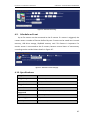
6.9. SCHEDULE AN EVENT ........................................................................................ 87
6.10.
7.
SPECIFICATIONS ........................................................................................... 87
CONCLUSION AND FUTURE WORK............................................................ 89
7.1. FUTURE WORK ................................................................................................ 90
REFERENCES ..................................................................................................... 91
vii
viii
List of Figures
FIGURE 1.1: PROJECT OVERVIEW. ............................................................................................. 1
FIGURE 1.2: IMAGE CAPTURE BLOCK DIAGRAM. ........................................................................... 3
FIGURE 1.3: MICROPROCESSOR IMPLEMENTATION. ...................................................................... 4
FIGURE 1.4: FINAL SYSTEM IMPLEMENTATION: THE CMOS CONTROLLER BLOCK MANAGES THE DATA
COMMUNICATION AND FRAME REQUESTS BETWEEN SDRAM 1 AND THE MICROPROCESSOR. ........ 4
FIGURE 2.1: AXIS 2100 NETWORK CAMERA [AXNE10]. .............................................................. 8
FIGURE 2.2: UNC-9211 IP CAMERA [HITE10]. ......................................................................... 9
FIGURE 2.3: VIVOTEK IP8161 IP CAMERA [5]. ......................................................................... 10
FIGURE 2.4: NETCAM XL IP CAMERA [STNE10]. ...................................................................... 10
FIGURE 2.5: IMAGE SENSORS: CCD (LEFT); CMOS (RIGHT) [AX06]. ............................................. 12
FIGURE 2.6: MJPEG ENCODES EACH FRAME INDEPENDENTLY [VIHA10]. ....................................... 15
FIGURE 2.7: MPEG-4 FINDS DIFFERENCES BETWEEN KEY FRAMES AND FOLLOWING FRAMES [VIHA10].
................................................................................................................................ 16
FIGURE 2.8: PROGRAMMING LANGUAGES USED TO DEVELOP EMBEDDED DEVICES [HAFU08]. ............ 24
FIGURE 2.9: DIGITAL INPUT SURVEILLANCE DEVICES [VIHA10]. .................................................... 28
FIGURE 2.10: DIGITAL OUTPUT SURVEILLANCE DEVICES [VIHA10]. ................................................ 28
FIGURE 3.1: THE DE2-70 BOARD [ALDE09]. ........................................................................... 33
FIGURE 3.2: QUARTUS II DESIGN FLOW [ALQU07]. ................................................................... 37
FIGURE 4.1: BLOCK DIAGRAM OF THE IMAGE CAPTURE BLOCK. ...................................................... 42
FIGURE 4.2: I2C SENSOR CONFIGURATION BLOCK. ..................................................................... 43
FIGURE 4.3: ACTIVE IMAGE CAPTURED BY THE CMOS SENSOR. .................................................... 43
FIGURE 4.4: CMOS SENSOR DATA CAPTURE BLOCK. ................................................................... 45
FIGURE 4.5: PIXEL COLOR PATTERN DETAIL [TECM09]. .............................................................. 46
FIGURE 4.6: RAW DATA TO RGB FORMAT BLOCK. ...................................................................... 46
FIGURE 4.7: SDRAM MEMORY BANKS [CNHO09]. ................................................................... 47
FIGURE 4.8: SDRAM CONTROL BLOCK. ................................................................................... 48
FIGURE 4.9: NIOS II PROCESSOR WITH PERIPHERALS. .................................................................. 50
FIGURE 4.10: NIOS II PROCESSOR CORE SETTINGS. ..................................................................... 51
FIGURE 4.11: INTERVAL TIMER SETTINGS.................................................................................. 52
ix
FIGURE 4.12: THE SDRAM CONTROLLER CONFIGURATIONS. ........................................................53
FIGURE 4.13: SPI (3 WIRE SERIAL) SETTINGS. ............................................................................55
FIGURE 4.14: MENUCONFIG BASIC SETUP AND KERNEL SETTINGS FOR THE FIRST BUILD. ......................60
FIGURE 4.15: NETWORKING SUPPORT OPTION. ..........................................................................62
FIGURE 4.16: DM9000 SUPPORT OPTION................................................................................62
FIGURE 4.17: FILESYSTEM SUPPORT CONFIGURATION. .................................................................62
FIGURE 4.18: ALTERA SPI CONTROLLER....................................................................................63
FIGURE 4.19: MMC/SD/SDIO OVER SPI................................................................................63
FIGURE 4.20: BOA SERVER OPTION. ........................................................................................64
FIGURE 4.21: ENABLE GENERIC CGI.........................................................................................64
FIGURE 4.22: FLOWCHART OF WEB SERVER. .............................................................................66
FIGURE 4.23: BASELINE SEQUENTIAL JPEG ENCODING. ...............................................................70
FIGURE 4.24: FLOWCHART OF JPEG COMPRESSION. ...................................................................70
FIGURE 4.25: IMAGE CAPTURE AND JPEG ENCODING DAEMON. ....................................................73
FIGURE 5.1: LIVE VIEW WEB PAGE. .........................................................................................76
FIGURE 5.2: IMAGE CAPTURED WITH 4X DIGITAL ZOOM. ..............................................................77
FIGURE 5.3: LIVE IMAGES WITH DIFFERENT EXPOSURE TIME. .........................................................78
FIGURE 5.4: ALTERA DE2-70 + CMOS SENSOR DEVELOPMENT KIT. ..............................................79
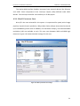
FIGURE 6.1: LANGUAGE SETTINGS. ..........................................................................................83
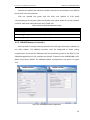
FIGURE 6.2: DATE AND HOUR SETTINGS. ..................................................................................84
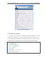
FIGURE 6.3: NETWORK SETTINGS. ...........................................................................................85
FIGURE 6.4: SECURITY PROPERTIES. .........................................................................................85
FIGURE 6.5: IMAGE PROPERTIES. .............................................................................................86
FIGURE 6.6: SCHEDULE A RECORDING. .....................................................................................87
FIGURE 6.7: SCHEDULE AN EVENT WEB PAGE. ............................................................................87
x
List of Tables
TABLE 2.1: FEATURES USAGE COMPARISON FOR CMOS AND CCD. ............................................... 13
TABLE 2.2: COMPARISON OF MJPEG, MPEG-4, H.264 [VIHA10]. ............................................ 17
TABLE 2.3: COMPARISON OF IPV4 AND IPV6 [VIHA10]. ............................................................ 18
TABLE 2.4: MAIN TRANSMISSION PROTOCOLS USED IN NETWORK CAMERAS [AX06]. ........................ 20
TABLE 2.5: OS SUPPORT FOR THE NIOS II PROCESSOR [HAFU08]. ................................................ 24
TABLE 3.1: COMPARISON BETWEEN FPGA AND ASIC [XIFP10]. .................................................. 32
TABLE 4.1: PARAMETERS AND SPECIFICATIONS OF THE CAMERA MODULE [TECM09]. ....................... 41
TABLE 4.2: I2C SENSOR CONFIGURATION SETTINGS. ................................................................... 44
TABLE 4.3: SDRAM SETTINGS. .............................................................................................. 47
TABLE 4.4: SUMMARY OF PARALLEL I/O MODULE SETTINGS. ........................................................ 53
TABLE 4.5: DM9000A MODULE SETTINGS. .............................................................................. 54
TABLE 4.6: FINAL SOPC SYSTEM. ........................................................................................... 58
TABLE 4.7: HWSELECT OPTIONS. ............................................................................................. 60
TABLE 5.1: MEMORY UTILIZATION. ......................................................................................... 75
TABLE 5.2: RUN-TIME ANALYSES TO CALCULATE FRAME RATE. ...................................................... 79
xi
xii
Acronyms
ADC
Analog-to-Digital Converter
CCTV
Closed-Circuit Television
CGI
Common Gateway Interface
DAC
Digital-to-Analog Converter
DCT
Discrete Cosine Transform
DMA
Direct Memory Access
DMIPS
Dhrystone Million Instructions Per Second
DVR
Digital Video Recorder
FPGA
Field-Programmable Gate Array
GPL
General Public License
I2C
Inter-integrated Circuit
IC
Integrated Circuit
IDE
Integrated Development Environment
IP
Internet Protocol
JPEG
Joint Photographic Experts Group
LCD
Liquid Crystal Display
MAC
Media Access Control
MCU
Minimum Coded Blocks
MMU
Memory Management Unit
MP3
MPEG-1/2 Audio Layer 3
MPU
Memory Protection Unit
NTSC
National Television System Committee
PAL
Phase Alternating Line
PDA
Personal Digital Assistant
PTZ
Pan Tilt Zoom
RTL
Register Transfer Level
SD
Secure Digital
SDRAM
Synchronous Dynamic Random Access Memory
SECAM
Sequential Colour with Memory
xiii
xiv
SPI
Serial Peripheral Interface
SSRAM
Synchronous Static Random Access Memory
TCP
Transport Control Protocol
UDP
User Datagram Protocol
URL
Uniform Resource Locator
USD
United States Dollars
VHDL
VHSIC Hardware Description Language
VHSIC
Very-High-Speed Integrated Circuit
USB
Universal Serial Bus
1. Introduction
This chapter presents the overall context of this project.
Firstly, a succinct
motivation for the project is presented, enhancing the importance of this kind of
systems in present days. After, a short background description of surveillance systems,
event management and Intelligent Video is given. Next, the project goals and tasks are
presented in a step-by-step approach, and finally, the organization of this thesis is
detailed.
1.1. Motivation
This project is the result of the work done in Embedded System Research Group
during the last year of the MSc in Industrial Electronics Engineering (Computer
Technology).
The main goal of this project is to design and implement a System-On-Chip (SoC),
in this case: an IP camera system. Although other commercial IP cameras do exist and
are feature rich, this project aims to architect a system where all the important
features for surveillance systems are implemented and be able to customize it and
include new features as requested by customers.
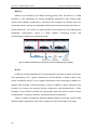
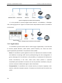
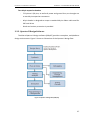
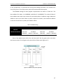
Figure 1.1 shows the project overview. The SoC prototype is based on an Altera
DE2-70 development board, using the TRDB-D5M 5 megapixel CMOS sensor, to
capture images. A host PC does the FPGA programming and is used for debugging,
through USB Blaster programming. The development board connects to the network,
through an Ethernet connection.
Figure 1.1: Project overview.
1
CHAPTER 1 – INTRODUCTION
IP Camera on FPGA with a Web Server
1.2. Surveillance System
“A surveillance system is a system design to process and monitor the behavior of
people, objects or processes within a given system for conformity to expected/desired
norms in trusted systems for security/social control. It can be either secrete or
evident” [CoDeGo08].
A video surveillance system connected through a data network offers several
advantages and advanced features that no analog surveillance system can support.
Among the advantages are: remote access from anywhere with a network connection;
high quality images (analog cameras have significant problems with interlacing scan
being difficult to capture fast-moving objects); event management and intelligent
video capabilities, with the possibility to schedule an event or implement software of
image analyses; ease of integration and the highest scalability, flexibility and economy.
[EzAr10]
1.3. Event Management and Intelligent Video
Now that cameras are increasingly affordable, surveillance systems are being
generalized all over the places. They are used in security systems as an answer to theft,
fraud and several kinds of attacks, in industry, in production lines and even to monitor
employees.
A frequent problem in surveillance systems is the large amount of recorded video
and little time to analyze it properly. Advanced network cameras with built-in
intelligence and analysis capabilities take care of this problem, reducing the amount of
recordings without interest and allowing programmed reactions.
Network cameras, duo to its worldwide connection and other built-in features like
motion detection, alarm, audio detection, active tampering, alarm connections, I/O
(input/output), and events management functions, allow a real-time operation. These
features allow network cameras to continuously analyze inputs to detect an event and
automatically react with the proper actions, such as video recording and sending alarm
notifications with a much better cost efficiency.
2
IP Camera on FPGA with a Web Server
CHAPTER 1 – INTRODUCTION
1.4. Goals
The main goal of this project is to fully implement an IP camera system on a FPGA.
This means, in terms of hardware, to implement a system with a soft-core processor,
memories, image acquisition, image processing blocks, and network capabilities. The
trade-off between the use of FPGA versus an ASIC is included in section 3.1.1.
For software, the system requires an operating system that supports an
application that deals with each frame acquired; furthermore a Web server and a
TCP/IP implementation, allowing live images to be viewed on Internet.
To achieve this, the project was split in several steps described below.
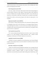
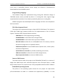
1.4.1. Image Capture
The aim of this first part was to implement video frames capture with the camera
sensor and save them on SDRAM memory. To test this block, an LCD (4.3’’ TRDB-LTM
from TERASIC [Te09]) is also connected to SDRAM memory. This way frames are
displayed on the LCD (Figure 1.2). This project is part of a broader project that includes
on the fly reconfiguration of some hardware and software characteristics.
Figure 1.2: Image Capture block diagram.
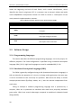
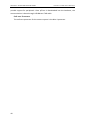
1.4.2. Microprocessor Implementation
Next step was to implement a microprocessor on FPGA, to run an operating
system and application software that includes a Web server and data processing
programs. Other specialized hardware blocks were implemented: Ethernet capabilities
to provide network access; a SDRAM module to control data exchange between
processor and SDRAM chip; a SD/MMC card interface and USB host, to save or read
data and add extra storage space if needed. More details in Figure 1.3.
3
CHAPTER 1 – INTRODUCTION
IP Camera on FPGA with a Web Server
Figure 1.3: Microprocessor implementation.
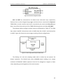
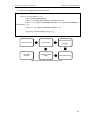
1.4.3. Complete IP Camera System
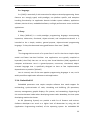
The final step was the assembling of all parts making the proposed system. The
image capture block and the microprocessor block, work in parallel. While each frame
is being stored in SDRAM 1, the microprocessor does its processing using SDRAM 2. In
Figure 1.4, a final implementation is presented.
Figure 1.4: Final system implementation: the CMOS Controller block manages the data communication and frame
requests between SDRAM 1 and the microprocessor.
1.5. Thesis outline
Besides this chapter, this document has 6 more chapters.
4
IP Camera on FPGA with a Web Server
CHAPTER 1 – INTRODUCTION
Chapter 2, Surveillance Systems, presents several concepts on surveillance
cameras systems and a survey on commercial solutions and research projects for IP
cameras.
Chapter 3, System Description, describes the FPGA as a prototyping system. The
FPGA development board and the IDE for FPGA development are presented; the final
system implementation on FPGA is also briefly described.
Chapter 4, Implementation, details the hardware and software design, explaining
all the tasks to build the final system. It makes reference to the image sensor and its
technical specifications; the implementation of the processor and its peripherals; the
implementation of the operating system; and finally, software blocks of the Web
server implementation and image compression.
Chapter 5, Testing & Experiments, describes the system validation, analyses
processor, memory utilization and system performance.
Chapter 6, Features and User Manual, presents all the features of the IP camera
system, as a manual. Here all configurations and settings are explained in the user
perspective.
The last chapter, Conclusion and Future Work, discusses the project and all the
work done. Further improvements and other ideas are suggested.
5
CHAPTER 1 – INTRODUCTION
6
IP Camera on FPGA with a Web Server
2. Surveillance Systems
The initial phase of this work consisted on a survey over IP cameras available in
the market and related research projects. The search was focused towards low-cost
products, mainly for surveillance purposes. The most relevant aspects are system
performance and price.
It was also done an overview of the basic building blocks available in a regular IP
camera, in terms of image sensor technology, processor, video compression, network
properties, and operating system.
2.1. State of the Art
The increasing widespread of Internet and the emergence of innovative
technologies led to a significant growth on IP based surveillance industry, over the past
few years. This section intent to provide an overview of existing solutions on the
market and also research projects.
2.1.1. Commercial Solutions
Nowadays a wide range of IP camera solutions exists, from tens to hundreds of
Euros. These prices differences have to do with the fact that there are different
application markets: stores, transports, schools, industrial, public surveillance, medical
care.
IP cameras can be divided in two types: fixed, and PTZ (Pan, Tilt and Zoom). While
fixed cameras have no motion or very limited motion, PTZ cameras can move
horizontally, vertically, and zoom in/out.
Some IP cameras can work during day and night. When the brightness decreases
to a certain level, the camera changes to night vision mode and uses infra-red (IR)
vision.
In terms of image resolution, cameras are available from 300k pixel to 5
megapixels. Latest IP cameras use a HDTV resolution with 1280x720 pixels. This higher
resolution means more data payload per frame, and to deal with this, it is needed the
7
CHAPTER 2 – SURVEILLANCE SYSTEMS
IP Camera on FPGA with a Web Server
use of image/video compression mechanisms. The most common used are Motion
JPEG, MPEG-4, and H.264.
All surveyed devices support TCP/IP to allow communication. Currently IPv4 (32bit address) is the most used, but there are also products with IPv6 (128-bit address).
Regarding level 4 protocols, IP cameras implements at least one of the transport
protocols: Transport Control Protocol (TCP), and User Datagram Protocol (UDP), but is
common to see cameras supporting both of them.
Next sections do an overview of IP camera devices available on the market from
the main companies. The cameras selected were those that roughly match those
characteristics required in this project.
AXIS 2100 Network Camera
The AXIS 2100 [AxNe10] is a low-cost IP camera that supports: TCP/IP, SMTP email, HTTP and other protocols. Configuration and management can be done via the
product’s own Web-based administration tools. It has external device connection with
IR-sensors, switches, and alarm relays. It has a BOA Web server working in a Linux
operating system. It delivers up to 10 images per second with a Motion JPEG
compression format. The selling price in October 2010 is $300.00 USD. [WeCa10]
Figure 2.1: Axis 2100 Network Camera [AxNe10].
Technical Specifications:
-
Networking: 10/100 Ethernet, with: TCP/IP, HTTP, FTP, SMTP, NTP, ARP, and
BOOTP.
-
I/O Connector: 1 optical-isolated alarm input. 1 digital output (max 24V,
100mA) with programmable digital input/output for remote image storage via
FTP or SMTP, pre/post alarm image storage.
8
-
Image Updating: Up to 10 frames/second over 10Mbps or 100Mbps networks.
-
Alarm Buffer: Up to 500kB memory available for pre/post alarm image storage.
IP Camera on FPGA with a Web Server
-
CHAPTER 2 – SURVEILLANCE SYSTEMS
Hardware: ARTPEC-1 compression chip; ETRAX-100, including, 32 bit RISC, 100
MIPS CPU, 8 MB RAM, 2 MB FLASH PROM.
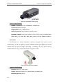
Gateway UNC-9211
The UNC-9211 [HiTe10] is a PTZ camera for domestic use. It is very versatile in
terms of resolution, and compression format; includes audio capability.
Figure 2.2: UNC-9211 IP Camera [HiTe10].
Technical Specifications:
-
Sensor type: Color 1/3’’ CCD Sensor (Sony).
-
Video compression: MPEG-4, Motion JPEG, H.263, and 3GPP.
-
Video frame rate: up to 30fps.
-
Communication protocol: HTTP, RTSP, FTP, SMTP, TCP/IP, UDP, ARP, ICMP,
DHCP, PPPoE, DDNS, UPnP, SAMBA, 3GPP.
-
System: 32-bit RISC CPU, 32MB RAM, and 4MB Flash.
-
Operating System: µClinux.
-
I/O connectors: 6 alarm input.
Vivotek IP8161
Vivotek IP8161 [Vi10] is a professional fixed network-camera. It is especially
suitable for wide open spaces such as building entrance and airports, or applications
requiring accurate identification, such as human faces in banks or vehicle license plates
in parking lots. Featuring a 2 megapixel sensor, this camera also has PTZ functions. It
works during day and night, and has a built-in SD/SDHC card slot for portable storage.
The selling price in October 2010 is $529.00 USD. [SeBe10]
9
CHAPTER 2 – SURVEILLANCE SYSTEMS
IP Camera on FPGA with a Web Server
Figure 2.3: Vivotek IP8161 IP Camera [Vi10].
Technical specifications:
-
System: TI DM365 SoC CPU, 256MB RAM, 128MB Flash.
-
Operating System: Linux 2.6
-
Image Sensor: 1/3.2’’ CMOS sensor.
-
Video Compression: H.264, MPEG-4, Motion JPEG.
-
Network Protocols: IPv4, IPv6, TCP/IP, HTTP, HTTPS, UPnP, RTSP/RTP/RTCP,
IGMP, SMTP, FTP, DHCP, NTP, DNS, DDNS, PPPoE, CoS, QoS, SNMP and 802.1x.
NetCam XL
The NetCam XL IP camera [StNe10] is specially designed to be used in street
environments. It has the ability to attach a weather station and display the current
weather data on the live images. According to [StNe10], the basic price starts at
$399.00 USD and can go to $699.00 USD for megapixel model.
Figure 2.4: NetCam XL IP Camera [StNe10].
Technical specifications:
10
-
Imaging: Sharp 1/3’’ CCD Sensor.
-
System: Motorola Coldfire CPU, 32MB DRAM, and 4MB Flash.
-
Operating System: µClinux.
IP Camera on FPGA with a Web Server
CHAPTER 2 – SURVEILLANCE SYSTEMS
-
Network Protocols: TCP/IP, HTTP, FTP, ARP, Telnet.
-
I/O Ports: 4 input alarms.
2.1.2. Research Projects
There are several projects regarding design IP cameras on FPGA technology. In
terms of FPGA, the most used are Spartan and Virtex from Xilinx [Xi10], and Cyclone
series from Altera [Al09]. Projects with Xilinx family FPGAs use mainly the embedded
PowerPC processor [XiPeRe10], although Microblaze [XiTo10] is an option too. With
the Altera FPGA development board, designers use the Nios II soft-core processor
[AlEmPr09], well-documented and fully supported by Altera.
The Elphel project [El10] implemented the 353/363 series camera. It uses the
ETRAX FS [AxEt10] processor running Linux that has support for multiple hardware
interfaces: 10/100 Ethernet; USB 1.1; RS-232. For video processing/compression it is
used the Xilinx Spartan 3E with 1200 logic elements. The system memory is a 64 MB
SDRAM, and 128 MB flash memory. Images are captured using a high-resolution 5
megapixels CMOS sensor. Elphel provides high performance cameras based on free
software and hardware designs. Users are free to buy Elphel cameras and change their
software/hardware design to create other products for new applications.
Another IP camera project [Gu07] developed in Instituto Superior Técnico uses the
Xilinx Virtex-4 FX FPGA with an embedded PowerPC 405 processor. The image sensor is
retrieved from a low-cost 1.3 megapixels sensor; memory has 64 MB SDRAM. The
software is implemented with the Xilinx Microkernel support. The Web server
implements a webpage that refreshes one frame per second; it is also possible to
change the brightness.
An intelligent IP Camera with motion detection implemented in FPGA was created
in Denmark [CoDeGo08]. The project was based on an Altera FPGA DE2-35
development board. The main purpose of this work is to record a video each time a
movement is detected, and save it on a SD-Card or make it accessible through an
Ethernet network. The motion detection algorithm is implemented using the Nios II
soft-core processor.
11
CHAPTER 2 – SURVEILLANCE SYSTEMS
IP Camera on FPGA with a Web Server
2.2. IP Camera Design
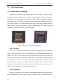
2.2.1. Image Sensor Technology
Based on the manufacturing process, there are two types of sensors: CMOS
(Complementary Metal Oxide Semiconductor) and CCD (Charge-coupled Device). Each
technology has its strengths and weaknesses that make it suitable for different
applications. The CCD sensors are produced with a technology created specifically for
the camera industry. The initial CMOS sensors used a technology standard that was
widely used in memory chips for PCs. Today’s CMOS sensors use a more specialized
technology, and sensor’s quality is increasing rapidly.
Figure 2.5: Image sensors: CCD (left); CMOS (right) [Ax06].
CCD Technology
A CCD is an analog shift register that conveys analog signals through successive
stages. The analog signals in each row of capacitors are transmitted and converted to
digital via an ADC IC. CCD sensors are used in cameras for more than 30 years, and
offer several advantages. In general, they still offer a slightly better sensitivity to light
and generate a bit less noise than CMOS sensors. A greater sensitivity to light
generates better images in low light conditions. However, CCD sensors are more
expensive and more complex to integrate in a camera. A CCD can also consume up to
100 times more energy than an equivalent CMOS sensor.
CMOS Technology
CMOS is a well-known and constantly developing manufacturing process used in
the semiconductors industry. Each pixel on a CMOS sensor is accompanied by an
12
IP Camera on FPGA with a Web Server
CHAPTER 2 – SURVEILLANCE SYSTEMS
amplifier based on a p-n junction structure. The p-n junction structure receives
photons from the sensor and transmits them to an image signal processor. Recent
advances in CMOS image sensors are bringing them close, in terms of image quality to
the CCD sensors. CMOS sensors reduce the total cost of the cameras, as they contain
all the required logic to manufacture the cameras. Compared to CCDs, CMOS sensors
offer more integration possibilities and more features. CMOS sensors also feature a
faster output (which is an advantage for higher resolution images), lower power
consumption and reduced size of the system. CMOS sensors with megapixel resolution
are more widely available and are less expensive than megapixel CCD sensors.
Table 2.1: Features usage comparison for CMOS and CCD.
CMOS
Features
Environment
CCD
-
High light sensitivity
Low cost
-
High color saturation
Widely used indoor
Widely used outdoor
-
Low power consumption
-
2.2.2. Soft-core Processors
There are two kinds of CPU cores for FPGA: hard and soft. Hardware based
processor is a specialized area of the FPGA integrated circuit. On the other hand, softcore processors are implemented using general-purpose FPGA logic cells. Main
embedded CPU soft-cores are: Nios II, MicroBlaze, PicoBlaze, and Leon.
Nios II
Nios II [AlEmPr09] is a proprietary 32-bit RISC architecture and a processor core
owned by Altera for use on their FPGAs. The soft-core nature of the Nios II processor
let the system designer implement and generates a custom Nios II core, taking in
account application’s specific requirements. Nios II functionality can be extended by
adding a MMU (Memory Management Unit), or creating custom instructions.
Nios II is available in 3 different configurations: Nios II/f (fast), Nios II/s (standard),
and Nios II/e (economy):
13
CHAPTER 2 – SURVEILLANCE SYSTEMS
-
IP Camera on FPGA with a Web Server
Nios II/f core is designed for maximum performance at the expense of core
size. Main features are: 6-stages pipeline, 1 instruction per cycle, optional
MMU and MPU, and hardware multiply.
-
Nios II/s core is designed to maintain a balance between performance and
cost. Main features are: 5-stages pipeline, 1 instruction per cycle, and
hardware multiply.
-
Nios II/e core is designed for smallest possible logic utilization of the FPGA.
Main features are: no pipeline, 1 instruction per 6 cycles, no supplementary
arithmetic blocks.
Nios II uses the Avalon switch fabric as interface to its embedded peripherals.
Multiple masters can operate simultaneously, using a slave-side arbitration scheme.
To configure and generate a Nios system, designers use the SOPC (System-On-aProgrammable Chip) builder, available in Quartus II package.
MicroBlaze
The MicroBlaze [XiTo10] is a 32-bit RISC soft-core processor designed for Xilinx
FPGAs. Many aspects of the MicroBlaze can be user configured: cache size, pipeline
depth (3-stages or 5-stages), embedded peripherals, memory management unit, and
bus-interfaces can be customized. On Virtex-5 FPGA family, processor speed can be up
to 210MHz.
Xilinx EDK (Embedded Development Kit) is the development package for building
Micro Blaze (and PowerPC) embedded processor systems in Xilinx FPGAs. It contains
the Micro Blaze core, peripheral cores, and the software development tools: GNU C
compiler, GNU debugger, Eclipse IDE.
Leon
LEON3 [AeGa10] is an open-source 32-bit architecture RISC processor. Main
features are: 7-stages pipeline; separated data cache and data instructions;
configurable cache; MMU; clock up to 125MHz in FPGA.
14
IP Camera on FPGA with a Web Server
CHAPTER 2 – SURVEILLANCE SYSTEMS
PicoBlaze
PicoBlaze [XiInPr10] is an 8-bit RISC architecture and a CPU core owned by Xilinx.
PicoBlaze was designed to operate in low-density FPGAs and occupy about 100
Spartan/Virtex slices. Some key features: 16 general purpose registers, up to 256
inputs/outputs ports.
2.2.3. Video Compression
Video compression technologies reduce file size with little or no negative effect on
visual quality. However, a high compression ratio may cause a trade-off between
bandwidth and image quality. Today, most network video compression vendors use
standard techniques to ensure compatibility and interoperability. Motion JPEG, MPEG4, and H.264 are the three major video compression technologies used by the IP
surveillance industry. Each technology has a different compression ratio and is
intended for different applications and purposes.
Motion JPEG
Motion JPEG or M-JPEG, announced by JPEG (Joint Photographic Experts Group), is
a digital video sequence consisting of a series of individual JPEG images [JpCo09]. One
advantage of Motion JPEG is that each image in a video sequence has the same quality
guaranteed, determinate by the compression level chosen for the network camera or
video encoder. Each frame is encoded and decoded independently without referring to
the previous or sequential frames (Figure 2.6). The main disadvantage of Motion JPEG
is that it does not use any video compression techniques to reduce data, because it is a
series of static images.
Figure 2.6: MJPEG encodes each frame independently [ViHa10].
15
CHAPTER 2 – SURVEILLANCE SYSTEMS
IP Camera on FPGA with a Web Server
MPEG-4
MPEG-4 was formed by the MPEG working group under ISO and IEC in 1998
[ViHa10]. It was developed for limited bandwidth applications that streams high
quality video. MPEG-4 implements a technique that compares key frames with next
sequential frames, leaving out redundant information and compressing only frame-toframe differences. This result in a large decrease of the original file size reducing the
bandwidth requirements. Figure 2.7 shows MPEG-4 comparing frames and
compressing only differences between frames.
Figure 2.7: MPEG-4 finds differences between key frames and following frames [ViHa10].
H.264
H.264 was initially developed by ITU (International Telecommunication Union) and
then published by JVT, a group combined by ITU and ISO/IEC, in 2003. H.264 is also
known as MPEG-4 part 10. It has a higher compression ratio comparing to MPEG-4 or
Motion JPEG [ViHa10]. H.264 technology is similar to MPEG-4, where sequential and
previous key frames are required during compression and decompression. H.264
provides a more efficient method for compression with more precise motion search
and prediction. It requires, however, more powerful CPU capabilities.
Table 3.1 shows a comparison between MJPEG, MPEG-4 and H.264, where H.264
features higher compression ratio, but at expense of a 10 times higher CPU usage.
16
IP Camera on FPGA with a Web Server
CHAPTER 2 – SURVEILLANCE SYSTEMS
Table 2.2: Comparison of MJPEG, MPEG-4, H.264 [ViHa10].
MJPEG
MPEG-4
H.264
Compressed file size
20%
2%
1%
Bandwidth
comparison ratio
20
2
1
Encoding CPU
loading ratio
1
4
10
-
Application
Local storage
Snapshot
viewing
-
-
Moving
picture
viewing
Real-time
transmission
-
-
Moving
picture
viewing
Real-time
transmission
2.2.4. IP Network
Different
network
technologies
are
used
to
provide
various
advantages of a networked video system. This section discusses communication over
the Internet using TCP/IP protocol; and presents an overview of the data transmission
protocols used in network video.
IP Address
Each network device has its identification, an IP address, from the level 3 protocol
employed – IP, Internet Protocol. Nowadays, there are two versions of IP: IP version 4
(IPv4) and IP version 6 (IPv6). The main difference between the two is that an IPv6 has
a much larger address space, using 128 bits against 32 bits of an IPv4 address. The
problem with IPv4 is that since the number of network devices is increasing at a very
fast pace, the IPv4 address space is rapidly nearing exhaustion, opening space to IPv6.
IPv4 addresses are grouped into four blocks, each separated by one point. Each block
represents a number between 0 and 255.
The following blocks of the IP address space are reserved for local networks:
-
10.0.0.0 ~ 10.255.255.255
-
172.16.0.0 ~ 172.31.255.255
-
192.168.0.0 ~ 192.168.255.255
All devices that must communicate over the Internet should have their own public
IP address. A public IP address is an address assigned by an Internet service provider
(ISP). An ISP may assign a dynamic IP address, which can change during a session, or a
17
CHAPTER 2 – SURVEILLANCE SYSTEMS
IP Camera on FPGA with a Web Server
static address. As so, an IPv4 address for a network camera can be assigned in two
main ways: 1) automatically, using DHCP where a dynamic address is assigned, and 2)
by manually entering a static IP address.
DHCP (Dynamic Host Configuration Protocol) automatically assigns a valid IP
address to a network device on the Internet. Assigning a fixed IP address to each
device will result in waste of IP addresses when the devices are not in operation. DHCP
tries to make more efficient use of the IP addresses.
The IPv6 standard consists of 128 bits, which are divided into eight parts, each
group containing four 16-bit digits. As said before, the main advantage of IPv6 is the
availability of a huge number of IP addresses, and the possibility of allowing a device to
automatically configure its IP address using its MAC address. Table 2.3 shows a
comparison between IPv4 and IPv6.
Table 2.3: Comparison of IPv4 and IPv6 [ViHa10].
Feature
IPv4
IPv6
Address space
32 bits
128 bits
Configuration settings
Manual
Auto
Priority control
No
Yes
Authentication
No
Yes
Transmission Protocols
This section introduces the two transmission protocols, in the TCP/IP stack: TCP
(Transmission Control Protocol) and UDP (User Datagram Protocol). These transport
protocols act as carriers for many other protocols. The HTTP (Hypertext Transfer
Protocol) is a layer 7, or application, protocol employed to browse Web pages on
servers around the world via the Internet, and it is carried by TCP. Other application
layer examples are FTP (File Transfer Protocols), SMTP (Send Mail transfer Protocols),
and RTP (Real-time Transport Protocol).
Transmission Control Protocol (TCP)
TCP creates a reliable transmission channel, based on connections. TCP handles
the task of dividing large blocks of data into smaller packets, and ensures that data
sent by one side is received at the other end. The reliability of TCP is achieved by
retransmission, but can cause considerable delays. In general, TCP is used when
18
IP Camera on FPGA with a Web Server
CHAPTER 2 – SURVEILLANCE SYSTEMS
reliable communication is more important than latency, thus providing better video
quality, but affecting real-time effect.
User Datagram Protocol (UDP)
UDP uses a simple transmission model without implicit hand-shaking dialogue to
provide reliability, ordering, or data integrity, leaving the whole control mechanism
and error checking over the higher protocols that needs it. Since UDP does not
perform any transmission of data losses, therefore does not introduce further delays,
being mainly used for time-sensitive responses and when the video quality is less
important.
Hypertext Transfer Protocol (HTTP)
HTTP works as a request-response protocol in the client-server computing model.
It is designed to allow users to view information on a web page through a browser.
Taking advantage of this feature, it is also a common way to display video images from
a network camera, where the video device works as a Web server, providing the video
stream to the user or application.
File Transfer Protocol (FTP)
FTP is used to upload and download files to and from a server. Several models
support an FTP client allowing to upload information from a network camera
(snapshots or video clips) to a FTP server, whenever an event occurs.
Send Mail Transfer Protocol (SMTP)
The SMTP is an internet standard for e-mail transmissions across Internet Protocol
networks. Some network cameras can send snapshots or notifications from the email
client implemented.
Real-time Transport Protocol (RTP)
The RTP is an Internet Protocol standard that specifies a way to manage real-time
transmissions. It runs on top of UDP, although it can use other transport protocols. RTP
components include a sequence number, to detect lost packets; a payload
identification, which describes the specific media encoding; frame identification, which
19
CHAPTER 2 – SURVEILLANCE SYSTEMS
IP Camera on FPGA with a Web Server
marks the beginning and end of each frame; and a source identification, which
identifies the frame’s originator. RTP is a common way to transmit videos and audio
with H.264/MPEG-4 compression format. On Table 2.4 there is a description of the
main protocols implemented on cameras.
Table 2.4: Main transmission protocols used in network cameras [Ax06].
Application Layer
Transport Layer
FTP
TCP
Data transfer over internet / intranet.
TCP
SMTP is specified for outgoing mail
SMTP
Description
transport.
TCP
HTTP
Designed for users to view information on a
web page through a browser.
UDP/TCP
RTP
Real-time multimedia streaming applications
that require time constraints.
2.3. Software Design
2.3.1. Programming Languages
This section describes the different programming languages, use in this project, for
different purposes. The FPGA configuration is specified using a hardware description
language (HDL) (2.3.2). High level languages are used in embedded OS (2.3.4).
2.3.2. Hardware Description Language (HDL)
The FPGA is generally configured using a HDL (Hardware Description Language). A
HDL can describe the operation of a circuit, its design and organization, the same way
it can be simulated to test and verify its operation. HDLs have the ability to model
multiple parallel blocks (flip-flops, adders, etc...) that can execute independent from
each other.
Taking as example a software programming language that is processed by a
compiler, HDLs use a synthesizer to transform HDL code into a physically realizable
gate netlist. HDLs have several advantages compared to traditional schematic-based
design [Pa03]:
20
IP Camera on FPGA with a Web Server
CHAPTER 2 – SURVEILLANCE SYSTEMS
- The design can be described at a very abstract level using HDLs;
- If a new technology emerges, designers do not need to redesign their circuit;
- Functional verification can be done early by using HDLs designs.
Verilog HDL and VHDL are the two most widely-used and well-supported HDL
implementations used in industry, but others HDL languages do exist, namely: AHDL,
MyHDL, Ruby, RHDL, SystemVerilog and SystemC.
Verilog
“The Verilog language is a hardware description language that specifies a digital
system at a wide range of levels of abstraction. The language supports the early
conceptual stages of design with its behavioral level of abstraction, and the later
implementation stages with its structural abstractions.” [ThMo02]
A Verilog design consists of a hierarchy of modules. Modules communicate with
each other through a set of declared input, output, and bidirectional ports. Inside a
module it is possible to have: net/variable declarations (wire, reg, integer ...),
concurrent and sequential statement blocks, and instances of other modules.
Sequential statements are placed inside a begin/end block and executed in sequential
order within the block.
VHDL
VHDL (VHSIC Hardware Description Language) [Co89] is a hardware description
language used in electronic design automation to describe digital and mixed-signal
system such as FPGA and integrated circuits. VHDL was created at the US Department
of Defense as a language for documenting designs. Nowadays a wide range of designs
are modeled in VHDL.
Every VHDL statement can be executed concurrently (VHDL is a parallel language).
Sequential steps can be also possible if explicit. Also, explicit time delays can be
achieved to execute a statement after a certain time. The key advantage of VHDL when
used for system design is that it allows the behavior of the required system to be
described (modeled) and verified (simulated) before synthesis tools translate that
design into real hardware (gates and wires).
21
CHAPTER 2 – SURVEILLANCE SYSTEMS
IP Camera on FPGA with a Web Server
Other companies promote other HDL languages for different reasons: some try to
reduce the complexity of designing in HDLs, raising the abstraction level of the design.
There are over a dozen of HDL languages, some still supported, and others are
outdated. Only main and current HDL languages are referenced.
AHDL
“The Altera Hardware Description Layer (AHDL) is a high level, modular language
especially suited for complex combinatorial logic, group operations, state machines,
and truth tables.” *SaSm00]
A disadvantage of AHDL is that it is proprietary. An advantage is that all language
constructs are synthesizable.
Handel-C
The Handel language is a subset of Occam used for hardware synthesis research at
Oxford University during the early nineties [Sh04]. It is a high level programming
language which targets low-level hardware. It contains all the necessary features to
describe complex algorithms.
2.3.3. High Level Software Programming Languages
A high level language is a programming language more abstract, easier to use, and
more portable across platforms. This abstraction is intended to make the language
user-friendly, simplifying the task for the creation of complex programs.
The terms high-level and low-level are relative. Some programmers may refer C as
low-level language, but in this thesis context C/C++ are considered high-level
languages.
C language
“C is a versatile, flexible, and powerful programming language that was designed
and developed in 1972.” *ReZi10+
A program written in C has functions and variables. Inside functions are
statements and the variables hold the results of computations. All variables must be
declared, either within a function or outside of any function.
22
IP Camera on FPGA with a Web Server
CHAPTER 2 – SURVEILLANCE SYSTEMS
C++ language
C++ [Sa95] is essentially C with extensions for object-oriented programming. Some
features are: strongly typed, multi-paradigm, not platform specific, and exception
handling functionality. Its application domain includes system software, application
software, device drivers, embedded software, and high-performance server and client
applications.
C Sharp
C Sharp [WiSh10] is a multi-paradigm programming language encompassing
imperative, declarative, functional, object-oriented, and component-oriented. It is
intended to be a simple, modern, general-purpose, object-oriented programming
language. “C sharp has borrowed many good features from Java.” *Ba08+
Java
“The language derives much of its syntax from C and C++ but has a simpler object
model and fewer low-level facilities. Java applications are typically compiled to
bytecode (.class files) that can run on any Java Virtual Machine (JVM) regardless of
computer architecture. Java is a general-purpose, concurrent, class-based, objectoriented language that is specifically designed to have as few implementation
dependencies as possible.”*WiJa10]
Java is currently one of the most popular programming languages in use, and is
widely used from application software to web applications.
2.3.4. Embedded OS
Embedded processors now require complex software that needs support for
multitasking, synchronization of tasks, scheduling and buffering I/O operations,
memory management, graphic displays, file systems, and networking. Supporting all
this services became harder when developing custom code. Nowadays, the time spent
developing needs to be shorter.
An OS (Operating System) can provide a wide list of features and services.
Software developers can work at a higher level of abstraction by using the API
(Application Programming Interface) of the operating system. An embedded OS
23
CHAPTER 2 – SURVEILLANCE SYSTEMS
IP Camera on FPGA with a Web Server
typically requires less processing power and has a smaller memory footprint than a
desktop OS. It also is likely to support booting from flash memory, produce ROMable
code, and to have I/O device drivers for the I/O devices that are more commonly found
in small devices. A C/C++ compiler is typically provided with the OS. Software
developing is almost done in C/C++ and usually come with a C/C++ compiler,
assembler, and debugging tools.
Nowadays, there are many open source operating systems. One of the most
known is µClinux.
A survey demonstrated that C language and derivates are the choice for the
majority of the embedded family development [HaFu08]. A detailed result of this
survey is shown in (Figure 2.8).
Figure 2.8: Programming languages used to develop embedded devices [HaFu08].
Several embedded operating systems are supported on the Nios II soft-core
processor as seen in (Table 2.5). Some are open source, others are commercial.
Table 2.5: OS support for the Nios II Processor [HaFu08].
Nios II IDE
Plug-in
OS
RTOS
OS Type
Company Name
eCos
YES
Open Source
eCosCentric
Euros RTOS
YES
Commercial
Euros
Erika Enterprise
YES
Commercial
Evidence
YES
Thread X
YES
Commercial
Express Logic
YES
MicroC/OS-II
YES
Commercial
Micrium
YES
embOS
YES
Commercial
Segger
Open Source
Community Supported
uClinux
24
YES
IP Camera on FPGA with a Web Server
CHAPTER 2 – SURVEILLANCE SYSTEMS
eCos, MicroC/OS-II, and µClinux are the most popular OS available for the Nios II
processor. Next sections take a detailed look at those embedded OS.
µClinux
The uClinux [EmLi10+ stands for “Microcontroller Linux”, and it is a fork of the
Linux kernel for microcontrollers without a memory management unit (MMU). Initially,
µClinux was targeted to the Motorola DragonBall family of embedded 68k processors.
Currently, µClinux includes Linux kernel releases for 2.0, 2.4, and 2.6 as well as a
collection of user applications, libraries and tool chains.
µClinux has support for several architectures, and forms the basis of several
embedded products: network routers, network cameras, security cameras, DVD, mp3
players, VoIP phones, scanners, and card readers.
An open source version [NiWi09] of uClinux has been ported to the Nios II
processor.
eCos
Embedded Configurable Operating System (eCos) [Ec10] is an open source,
royalty-fee, real-time operating system intended for embedded systems and
applications which need only one process with multiple threads. It is designed to be
customizable for application requirements to deliver the best possible run-time
performance and minimize hardware needs. It is implemented in C/C++ and has
compatibility layers and API for POSIX and uTRON.
eCos was designed for devices with memory size in the tens of hundreds of
kilobytes, or with real-time requirements. A minimum of 2 MB of RAM is needed, not
including application and service needs. eCos runs on a wide variety of hardware
platforms, including: ARM, IA-32, Motorola 68k, MIPS, Nios II, PowerPC, and SPARC.
At the beginning managed by Cygnus, eCos is now free software developed by a
community ensuring on-going technical innovation and platform software.
MicroC/OS-II
MicroC/OS-II [Mi10] is a highly portable, scalable, preemptive, real-time,
multitasking kernel for microprocessors and microcontrollers. It is written in C for
25
CHAPTER 2 – SURVEILLANCE SYSTEMS
IP Camera on FPGA with a Web Server
maximum portability. It is currently maintained by Micrium Incorporation and can be
licensed on product line basis. Micrium also created other middleware software
products such as uC/OS-View, uC/CAN, uC/TCP-IP, uC/FS, uC/GUI, uC/MOD-BUS,
uC/LCD, uC/USB (Mass Storage Device and Bulk) and a large assortment of uC/TCP-IP
applications such as client software for DHCP, POP3, SNTP, FTP, TFTP, DNS, SMTP, and
TTCP.
MicroC/OS-II can manage up to 255 tasks and provides services such as
semaphores, mutual exclusion semaphores, event flags, message mailboxes, message
queues, task management, fixed-size memory block management, and time/timer
management [Mi10].
Altera has ported MicroC/OS-II to the Nios II processor. Altera distributes
MicroC/OS-II in the Nios EDS, and supports the Nios II implementation of the
MicroC/OS-II kernel.
MicroC/OS-II is suitable to use on a wide-range of applications: Avionics, Medical
Equipment/Devices, Data Communications Equipment, White Goods (Appliances),
Mobile Handsets, Industrial Controls, Consumer Electronics, Automotive, and other
embedded applications.
Nios II microC/OS-II has a free license for universities and students provided by
Micrium.
RTEMS
The Real-Time Executive for Multiprocessor Systems (RTEMS) [Rt10] is a full
featured real-time operating system that supports a variety of open API and interface
standards. RTEMS does not provide any form of memory management or process. Its
design has been ported to various target processors architectures: ARM, ATMEL AVR,
Blackfin, x86, 68k, MIPS, Nios II, PowerPC, and SPARC.
FreeRTOS
FreeRTOS [Fr10] is a portable, open source, royalty fee, mini real time kernel. It is
distributed under the GPL. Some supported architectures are: ARM, Atmel AVR, Micro
Blaze, x86, 8052, Coldfire, and Nios II.
26
IP Camera on FPGA with a Web Server
CHAPTER 2 – SURVEILLANCE SYSTEMS
2.4. IP Surveillance Overview
The development of innovative technologies and rapid expansion of Internet
usage, led to a growth of IP surveillance industry, driving changes in the video
surveillance market. IP surveillance is increasing its importance in the video
surveillance market, mainly with IP cameras.
An IP surveillance system consists of an IP camera that transmits a sequence of
images, allowing users to view and manage the video and image remotely with a
networked device, such as a personal computer. Other components can also be part of
an IP surveillance system depending on the needs: a video server, a network video
recorder, and central management software.
2.4.1. Video Management
An IP surveillance system must include video management to achieve reliability,
flexibility, scalability and high efficiency. Video management provides basic
monitoring, recording and management functions, and advanced functions as
intelligent surveillance. Usually video management software is included in IP camera’s
Web server and these functions are performed by the IP camera itself.
Users can view live video images with a Web browser, and it is possible to allow
more than one user to access the images.
Recording can be performed in different modes. Each time the user desires to
record, the IP camera does a continuously recording. It is possible to schedule a period
of recording, where the IP camera records the video and then store all data, giving the
possibility to the user to watch the video whenever needed. Other option is to record
only when a specific event is triggered.
It is possible to connect digital input devices. In surveillance systems these devices
are alarms and sensors: anti-glass break sensors, active infrared sensors, smoke
sensors, and passive infrared sensor, and other type of sensors. Figure 2.9 shows
various input devices available to connect to an IP camera.
27
CHAPTER 2 – SURVEILLANCE SYSTEMS
IP Camera on FPGA with a Web Server
Figure 2.9: Digital input surveillance devices [ViHa10].
It is also possible to connect digital output devices: a soundalarm, a flashlight
alert, warning signals etc. Figure 2.10 shows some output devices used in surveillance
environment.
Figure 2.10: Digital output surveillance devices [ViHa10].
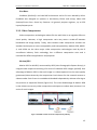
2.4.2. Applications
IP surveillance systems can be used in a wide-range of applications. It can be used
to monitor people behavior, public places, specific facilities, etc. There are some
typical application possibilities in key business areas [Ax06]:
-
Stores: IP surveillance system applied in stores can decrease the number of thefts
and robberies, increasing staff’s security and optimizing the store management. A
great advantage of IP surveillance is the possibility to implement EAS (Electronic
Article Surveillance) in the store, where each stolen product is reported
immediately and recorded. IP cameras are not only used for surveillance, they can
monitor costumer’s habits and register most visited areas.
-
Transportation: IP surveillance can increase security in airports, highways, train
stations, and other transport systems. IP cameras can also be used to monitor city
traffic.
28
IP Camera on FPGA with a Web Server
-
CHAPTER 2 – SURVEILLANCE SYSTEMS
Education: From elementary schools to university, IP surveillance helps to avoid
vandalism and increasing security for students, teachers and staff. IP cameras can
be used for remote learning for students who cannot attend school.
-
Industrial environment: IP cameras can monitor production lines, verifying the
correctness of the assembly process. In the office, IP cameras can provide videoconferencing.
-
Streets surveillance: IP surveillance is a basic tool to fight against crime and protect
citizens. Police can have access to these cameras and every time an irregular
situation is detected, a quick response can be guaranteed.
-
Government: Public buildings, museums, offices, libraries, prisons can be
protected by IP cameras 24 hours a day. With an intelligent system is also possible
to do people counting, and elaborate statistics.
-
Medical care: IP surveillance increases the security of staff, patients, and visitors.
Doctors can monitor patients from any place that has an Internet connection.
29
CHAPTER 2 – SURVEILLANCE SYSTEMS
30
IP Camera on FPGA with a Web Server
3. System Analysis and Design
This chapter presents the system constraints analysis, in terms of FPGA, processing
time and data consistency. It also presents the FPGA development board used for IP
camera design and the Quartus II design software.
All choices for the implemented system are described, in terms of programming
language, FPGA development board, CMOS sensor used, embedded operating system
and the soft-core processor.
3.1. System constrains analysis
This section gives an overview of the different constraints of the system.
3.1.1. FPGA constraints
One of the first constraints in camera system development is to evaluate the
implementation of the IP camera system with all necessary features on a FPGA
platform.
FPGA definition
A field-programmable gate array is a logic device that contains a two-dimensional
array of generic logic cells and programmable switches. A logic cell can be configured
to perform a simple function, and a programmable switch can be customized to
provide interconnections among logic cells. A custom design can be implemented by
specifying the function of each programmable switch [Ch08].
FPGA versus ASIC
Compared to ASICs the flexibility of a FPGA is at the same time its weakness in
terms of area, delay and power consumption: 20 to 35 times more area is required, 3
to 4 times slower in speed performance, and consumes roughly 10 times more energy.
Despite these disadvantages, FPGAs present an alternative for digital system
implementation mainly for small enterprises or small entities [Ch08] as it has a shorter
31
CHAPTER 3 – SYSTEM ANALYSES AND DESIGN
IP Camera on FPGA with a Web Server
time-to-market and cheaper costs for a reasonable amount of systems. Table 3.1
summarizes FPGA advantages and ASIC advantages.
Table 3.1: Comparison between FPGA and ASIC [XiFp10].
FPGA Design Advantages
ASIC Design Advantages
Faster time-to-market
Full custom capability
Development cost cheaper
Lower unit costs
More predictable project cycle
Smaller form factor
Field reprogramability
Higher raw internal clock speeds
Requirements for the FPGA Development Board
-
Support / documentation / examples available and up to date;
-
Input / output for camera sensor;
-
SD/MMC Card Slot for adding extra storage space and firmware update
option;
-
USB host connector;
-
Possibility to add a soft-core processor;
-
Enough memory for video frame.
3.1.2. Time constraint
Time constraints are an important subject in an IP camera system. The image
capture, processing and buffering needs to be fast enough, avoiding bottlenecks. On
the other hand, software needs to take into account execution speed. It is important
to have efficiency in image compression algorithm. Time constraints are related to
data constraints (3.1.3).
3.1.3. Data constraint
To buffer captured frames, temporary data memory needs to have enough space
to allocate several frames. The other constraint regards to the image type format.
Main encoding algorithms work with RGB and YUV format.
The soft-core processor needs a minimum amount of RAM to accomplish its task.
This amount of memory depends on which embedded OS is running, video frame
payload, and executing programs needs.
32
IP Camera on FPGA with a Web Server
CHAPTER 3 – SYSTEM ANALYSES AND DESIGN
Storage expansion using external SD/MMC Card or USB pen drive is also a
requirement in order to store video streams.
3.2. FPGA Development Board
The DE2-70 development board features a Cyclone II FPGA chip [AlDe09]. All main
board components are connected to the chip pins, allowing the user to configure the
connections between them as desired. The DE2-70 board includes switches, LEDs, 7segment displays, and a 16 x 2 character display. If memory is needed, it is also
available SSRAM, SDRAM, and Flash memory chips. For experiments that require a
processor, it is possible to instantiate Altera’s Nios II processor, and for simple
input/output interfaces, RS-232 and PS/2 connectors are available. For more complex
design projects, it is possible to use USB and Ethernet connectors, a SD/MMC Card slot,
and two expansion headers.
The software provided with DE2-70 board is the Quartus II Web Edition design
tools.
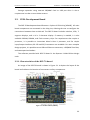
3.2.1. Characteristics of the DE2-70 board
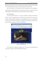
An image of the DE2-70 board is shown in Figure 3.1. It depicts the layout of the
board and indicates the location of connectors and key components.
Figure 3.1: The DE2-70 Board [AlDe09].
33
CHAPTER 3 – SYSTEM ANALYSES AND DESIGN
IP Camera on FPGA with a Web Server
Detailed information about DE2-70 Development Board [AlDe09]:
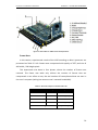
Cyclone II 2C70 FPGA
-
68,416 Logic Elements
-
250 M4K RAM blocks
-
1,152,000 total RAM bits
-
150 embedded multipliers
-
4 PLLs (Phase-Locked Loop)
-
622 user I/O pins
-
Fine Line BGA 896-pin package
Serial Configuration device and USB Blaster circuit
-
Altera’s EPCS16 Serial Configuration device
-
On-board USB Blaster for programming and user API control
-
JTAG and AS programming modes are supported
SSRAM (Synchronous Static Random Access Memory)
-
2-Mbyte standard synchronous SSRAM
-
Organized as 512K x 36 bits
-
Accessible as memory for the Nios II processor and by the DE2-70 Control
Panel
SDRAM
-
Two 32-Mbyte Single Data Rate Synchronous Dynamic RAM memory chips
-
Organized as 4M x 16 bits x 4 banks
-
Accessible as memory for the Nios II processor and by the DE2-70 Control
Panel
Flash memory
-
8-Mbyte NOR Flash memory
-
Support both byte and word mode access
-
Accessible as memory for the Nios II processor and by the DE2-70 Control
Panel
SD card socket
-
Provides SPI (Serial Peripheral Interface) and 1-bit SD mode for SD Card
access
34
IP Camera on FPGA with a Web Server
-
CHAPTER 3 – SYSTEM ANALYSES AND DESIGN
Accessible as memory for the Nios II processor with the DE2-70 SD Card
Driver
Pushbutton switches
-
4 pushbutton switches
-
Debounced by a Schmitt trigger circuit
-
Normally high; generates one active-low pulse when the switch is pressed
-
Toggle switches
18 toggle switches for user inputs
-
A switch causes logic 0 when in the DOWN (closest to the edge of the DE270 board) position and logic 1 when in the UP position
Clock inputs
-
50-MHz oscillator
-
28.63-MHz oscillator
-
SMA external clock input
Audio CODEC
-
Wolfson WM8731 24-bit sigma-delta audio CODEC
-
Line-level input, line-level output, and microphone input jacks
-
Sampling frequency: 8 to 96 KHz
-
Applications for MP3 players and recorders, PDAs, smart phones, voice
recorders, etc.
VGA output
-
Uses the ADV7123 140-MHz triple 10-bit high-speed video DAC
-
With 15-pin high-density D-sub connector
-
Supports up to 1600 x 1200 at 100-Hz refresh rate
-
Can be used with the Cyclone II FPGA to implement a high-performance TV
Encoder
NTSC/PAL/ SECAM TV decoder circuit
-
Uses two ADV7180 Multi-format SDTV Video Decoders
-
Supports worldwide NTSC/PAL/SECAM color demodulation
-
One 10-bit ADC, 4X over-sampling for CVBS
-
Supports Composite Video (CVBS) RCA jack input
35
CHAPTER 3 – SYSTEM ANALYSES AND DESIGN
-
IP Camera on FPGA with a Web Server
Supports digital output formats: 8-bit ITU-R BT.656 YCrCb 4:2:2 output + HS,
VS, and FIELD Applications: DVD recorders, LCD TV, Set-top boxes, Digital
TV, Portable video devices, and TV PIP (picture in picture) display.
10/100 Ethernet controller
-
Integrated MAC and PHY with a general processor interface
-
Supports 100Base-T and 10Base-T applications
-
Supports full-duplex operation at 10 Mb/s and 100 Mb/s, with auto-MDIX
-
Fully compliant with the IEEE 802.3u Specification
-
Supports IP/TCP/UDP checksum generation and checking
-
Supports back-pressure mode for half-duplex mode flow control
USB Host/Slave controller
-
Complies fully with Universal Serial Bus Specification Rev. 2.0
-
Supports data transfer at full-speed and low-speed
-
Supports both USB host and device
-
Two USB ports (one type A for a host and one type B for a device)
-
Provides a high-speed parallel interface to most available processors;
supports Nios II with a Terasic driver
-
Supports Programmed I/O (PIO) and Direct Memory Access (DMA);
Serial ports
-
One RS-232 port
-
One PS/2 port
-
DB-9 serial connector for the RS-232 port
-
PS/2 connector for connecting a PS2 mouse or keyboard to the DE2-70
board
IrDA transceiver
36
-
Contains a 115.2-kb/s infrared transceiver
-
32 mA LED drive current
-
Integrated EMI shield
-
IEC825-1 Class 1 eye safe
-
Edge detection input
IP Camera on FPGA with a Web Server
CHAPTER 3 – SYSTEM ANALYSES AND DESIGN
Two 40-pin expansion headers
-
72 Cyclone II I/O pins, as well as 8 power and ground lines, are brought out
to two 40-pin expansion connectors
-
40-pin header is designed to accept a standard 40-pin ribbon cable used for
IDE hard drives
-
Diode and resistor protection is provided
3.2.2. Quartus II Design Software
The Altera Quartus II design software [AlQu07] provides a complete, multiplatform
design environment. Figure 5 shows an illustration of the Quartus II design flow.
Figure 3.2: Quartus II design flow [AlQu07].
37
CHAPTER 3 – SYSTEM ANALYSES AND DESIGN
IP Camera on FPGA with a Web Server
The design flow involves the following steps [ShPa10]:
-
Design Entry – the desired circuit is specified either by means of a
schematic diagram, or by using a hardware description language, such as
Verilog or VHDL.
-
Synthesis – the entered design is synthesized into a design implementation
in terms of logic gates.
-
Place & Route – establishes the placement of the logic elements defined in
the netlist into the logic elements (LE) in an actual FPGA chip.
-
Timing Analysis – analyzes propagation delays along the various paths in
the fitted circuit, to provide an indication of the expected performance of
the circuit.
-
Simulation – functional or timing simulation is performed.
-
Programming & Configuration - the designed circuit is implemented in a
physical FPGA chip by programming the configuration switches that
configure the LEs and establish the required wiring connections.
3.2.3. ModelSim-Altera
Mentor Graphics Corporation’s ModelSim-Altera version 6.5b software is included
in the Quartus II version 9.1 design software. It performs a functional and a timing
simulation of a Quartus II-generated design containing Verilog HDL, VHDL, or both.
The ModelSim-Altera software gives designers advanced test bench capabilities
for faster simulation and faster time-to-market. Test benches can be written in the
same language as the design source code, i.e, Verilog HDL, as the original design. Test
benches can apply stimulus to a module and monitor its outputs. Test benches can
monitor outputs and appropriate messages or warnings can be displayed as required
by the user [Hd10].
3.3. A short Overview of the Implemented System
The hardware system design implied the implementation of image acquisition and
image processing blocks, a soft-core processor, and other necessary blocks. On the
38
IP Camera on FPGA with a Web Server
CHAPTER 3 – SYSTEM ANALYSES AND DESIGN
other hand, in embedded software system design, the software is developed and
downloaded to the embedded system.
Programming Language
The hardware design was implemented using Verilog HDL. Reference design of
TRD-D5M camera sensor provided by Altera is in Verilog HDL. Also, original image
acquisition block and other IP core blocks provided by Altera are in Verilog HDL.
Software programs were developed under C language and later cross-compiled to
Nios II processor.
FPGA Development Board
The project was implemented using an Altera DE2-70 FPGA Board. The Cyclone II
FPGA with 70.000 logic elements allows the full implementation of the IP Camera
System. The Altera DE2-70 board features used are:
-
USB Blaster for FPGA programming and Debug;
-
32-MB SDRAM-1 to be used as frame images buffer;
-
32-MB SDRAM-2 to be used as Nios II processor SDRAM;
-
SD-Card Socket to allow the use of SD/MMC Cards. This memory card can
be used as storage card or to update firmware;
-
Pushbuttons/switch to control CMOS sensor exposure time, restart system,
and other configurations;
-
10/100 Ethernet controller to provides networking connections;
-
USB Host controller to allow the use of USB storage devices;
-
40-pin expansion header to connect a CMOS camera;
Camera CMOS sensor
The camera sensor used in this project is the TRDB-D5M [TeCm09]. It is a Micron 5
Mega Pixel CMOS sensor with controlled exposure time and output data is in RGB
Bayer Pattern format. This camera sensor is fully compatible with Altera DE2-70 Board.
Embedded Operating System
The µClinux is the operating system chosen for this project. An open-source
µClinux-distribution for NIOS II is available and supported by [NiWi09]. It is also
39
CHAPTER 3 – SYSTEM ANALYSES AND DESIGN
IP Camera on FPGA with a Web Server
provide support for peripherals. Once µClinux is downloaded into the hardware, the
communication is done through USB Blaster JTAG cable.
Soft-core Processor
The soft-core processor for the camera system is the Nios II processor.
40
4. Implementation
4.1. Camera Hardware Module
4.1.1. Technical specifications
The camera employed in this project is the Terasic TRDB-D5M [TeCm09], a CMOS
sensor development kit with 5 mega pixel. The active pixel array of the CMOS sensor
consists of 2,592-columns by 1,944-rows and a frame rate up to 15fps with full
resolution (2592 x 1944) or 150fps when using VGA resolution (640 x 480).
The Terasic TRDB-D5M module has up to 256 configurable registers, and can be
programmable using simple two-wire serial interface. This configuration is done on a
FPGA block – I2C_CCD_Config (4.1.2), written in Verilog HDL. The main programmable
parameters are: resolution, frame rate, and exposure time.
The resolution of the output image is the full width and height chosen, but it can
be reduced without affecting field-of-view: using Skipping and Binning [TeCm09]. In
Skipping mode, entire rows and columns of pixels are not sampled. The 2X or 3X mode
skips one or two “Bayer” pair of pixels, respectively, for every pair output. Binning
reduces resolution by combining adjacent same-color pixels to produce one output
pixel. Table 4.1 summarize the technical specifications of the TRDB-D5M module:
Table 4.1: Parameters and specifications of the camera module [TeCm09].
Parameter
Value
Active Pixels
2,592H x 1,944V
Pixel Size
2.2µm x 2.2µm
Color Filter Array
RGB Bayer Pattern
Maximum Data rate / Master Clock
96Mp/s at 96MHz
Frame Rate
Full Resolution
Up to 15fps
VGA (640 x 480)
Up to 150fps
ADC Resolution
12-bit
Responsivity
1.4 V/lux-sec (550nm)
Pixel Dynamic Range
70.1dB
Power
3.3 V
41
CHAPTER 4 – IMPLEMENTATION
IP Camera on FPGA with a Web Server
4.1.2. Image Capture
The image capture operation is divided into other tasks. First it is required to
configure the camera sensor. In operation a raw image from the camera sensor is
captured, translated to RGB (Red, Green, and Blue) format and temporarily stored in
SDRAM, frame by frame. These blocks were originally provided by Altera and changes
were made to adapt them to the project requirements, in terms of image capture
resolution and SDRAM’s configuration to meet frame data size. Figure 4.1 represents
the block diagram of the image capture.
Figure 4.1: Block diagram of the image capture block.
I2C Sensor Configuration
The Verilog HDL module that configures programming registers from the camera is
called I2C_CCD_Config.v. This HDL file was originally written by Altera. Only
configuration values were changed.
The purpose of this module is to control and configure: exposure time, resolution,
and frame rate. This block uses the two-wire serial interface bus to communicate with
TRDB-D5M registers.
“I2C is a multi-master serial single-ended computer bus developed by Philips that
is used to attach low-speed peripherals to a motherboard, embedded system, or cell
phone.”*IcBu10]. Figure 4.2 shows the I2C sensor configuration block: inputs and
outputs.
42
IP Camera on FPGA with a Web Server
CHAPTER 4 – IMPLEMENTATION
Figure 4.2: I2C Sensor configuration block.
iCLK and iRST are connected to the board main clock and reset, respectively.
Exposure time can be changed using toggle switches that are connected to iExposure.
TRDB-D5M is a serial interface slave and is controlled by the serial clock I2C_SCLK and,
data is transferred into and out of the TRDB-D5M through the serial data I2C_SDAT.
The settings used to configure camera sensor are displayed on Table 4.2. The Row
Start value is 0x023F, Column Start value is 0x458, Row Size is 0x31F, and Column Size
is 0x1DF. Figure 4.3 shows the active image resulting of these configurations.
Figure 4.3: Active image captured by the CMOS sensor.
The Binning x3 is the sub sampling mode used to reduce by one quarter the
output resolution. The field-of-view covers 800x480 pixels, leading to an output
resolution of 400x240. Default exposure time can be changed to a higher or lower
value, depending on the brightness of the environment.
43
CHAPTER 4 – IMPLEMENTATION
IP Camera on FPGA with a Web Server
Table 4.2: I2C Sensor configuration settings.
Register Description
Value Hex
Mode
Row Start
0x023F
Column Start
0x0458
Row Size
0x031F
Column Size
0x01DF
Row Address Mode
0x033
X3 Binning
Column Address Mode
0x033
X3 Binning
Exposure Time
0x0500
Each configuration has 24 bit width, where 8 bits are for register identification and
16 bits for register value.
assign sensor_start_row
assign sensor_start_column
assign sensor_row_size
assign sensor_column_size
assign sensor_row_mode
assign sensor_column_mode
= 24'h01023F; //Start Row at 575.
= 24'h020458; //Start Column at 1112
= 24'h0301DF; //Row Size is 800
= 24'h04031F; //Column Size is 480
= 24'h220011; //Binning Row mode
= 24'h230011; //Binning Column mode
CMOS Sensor Data Capture
The Verilog HDL file implementing the module that handles data capture from the
camera is called CCD_Capture.v. It was provided by Altera and no change was needed
for this design.
This module gets raw data from the camera sensor and sends raw data with X and
Y coordinates to next module. Figure 4.4 shows CCD_Capture block with inputs and
outputs.
44
IP Camera on FPGA with a Web Server
CHAPTER 4 – IMPLEMENTATION
Figure 4.4: CMOS sensor data capture block.
iCLK and iRST are connected to board main clock and reset, respectively. iSTART
and iEND are connected to toggle switches. iSTART is the signal to start reading raw
data from sensor and calculates X and Y coordinates. iFVAL, iLVAL, and iDATA are sent
by the camera sensor. Each time a valid line is set, iLVAL value is 1, and when camera
sensor has a valid frame, iFVAL value is set to 1. iDATA represents raw data from
camera sensor.
This module has five data outputs. When a pixel is ready to be sent, oDVAL value
is 1. Raw data is sent by oDATA signals. This module calculates X and Y coordinates and
sends these values on oX_Cont and oY_Cont.
Bayer Color Pattern Data to 30-bit RGB
The raw data from camera is divided into Red, Green and Blue colors by the
module RAW2RGB.v. It was provided by Altera and no change was needed for this
design.
This module uses the X and Y coordinates to determinate RGB values. Pixels are
output in a Bayer pattern format (Figure 4.5) consisting of four colors: green1, green2,
red, and blue [TeCm09]. “Each primary color does not receive an equal fraction of the
total area because the human eye is more sensitive to green light than both red and
blue light. Redundancy with green pixels produces an image which appears less noisy
and has finer detail than could be accomplished if each color were treated equally”
[UnDi10]. The first raw outputs data alternates between green1 and red pixels, and the
second raw output alternates between blue and green2 pixels. The green1 and green2
have the same colour filter and are outputted as green.
45
CHAPTER 4 – IMPLEMENTATION
IP Camera on FPGA with a Web Server
Figure 4.5: Pixel Color Pattern Detail [TeCm09].
Figure 4.6: Raw data to RGB format block.
The iCLK is connected to main clock and iRST to main reset signal. iDVAL checks
when a pixel is ready, and reads each pixel using iDATA. iX_Cont and iY_Cont give the
exact coordinates of the pixel, helping to calculate oRed, oGreen, and oBlue value. For
each valid frame, oDVAL is 1.
Multi-Port SDRAM Controller
This module is the SDRAM chip controller. The Verilog HDL file for this module is
the Sdram_Control_4port.v; originally provided by Altera, changes were made in terms
of read and write addresses.
Frames are temporarily stored in the SDRAM. Altera DE2-70 Development Board
has two “IS42S16160B 256-MBit synchronous DRAM”, but this module uses only one
46
IP Camera on FPGA with a Web Server
CHAPTER 4 – IMPLEMENTATION
of the 32 MB chips. To optimize the writing and reading operations, this module uses
four FIFO (First In First Out) stacks, with dual-read and dual-write ports.
The SDRAM settings to meet project requirements are shown in Table 4.3. The
base address for Write 1 is 0x000000, and Write 2 is 0x200000. The value of Write 2
base address was taken into account to not overlap Write 1 address range. Maximum
address is the size of each frame in pixels. In Write 2 or Read 2, the maximum address
is the size of the frame in pixels plus address offset.
Table 4.3: SDRAM settings.
Write 1
Write 2
Read 1
Read 2
Address
0x000000
0x200000
0x000000
0x200000
Maximum Address
0x017700
(400x240)
0x2189C0
(Address + 400x240)
0x017700
(400x240)
0x2189C0
(Address + 400x240)
One of the banks stores 10 bit for red color and 5 bit for green color, the other
bank stores other 5 bit of green color plus 10 bit of blue color (Figure 4.7).
Figure 4.7: SDRAM memory banks [CnHo09].
47
CHAPTER 4 – IMPLEMENTATION
IP Camera on FPGA with a Web Server
Figure 4.8: SDRAM control block.
CLK is connected to main clock. RD1_CLK and RD2_CLK are connected to clock
signal of the module that reads frames from SDRAM. Each time a pixel needs to be
read from SDRAM, RD1 and RD2 are set high to request pixel reading, and when
request is carried out, RD1_LOAD and RD2_LOAD are set high and the pixel’s memory
position is cleared. WR1_CLK and WR2_CLK are connected to RAW2RGB module’s
clock to have data synchronized. When a pixel from RAW2RGB module is ready, WR1
and WR2 are set high to request data writing. WR1_ADDR, WR2_ADDR, RD1_ADDR,
and RD2_ADDR read start addresses; WR1_MAX_ADDR, WR2_MAX_ADDR,
RD1_MAX_ADDR, and RD2_MAX_ADDR read end addresses for reading or writing.
CKE is the SDRAM clock enable, WE_N is the SDRAM write enable, CS_N is the chip
select, and BA is the SDRAM bank address. RD1_DATA with 16-bit bus width consists
on 5-bit for green color and 10-bit for blue color; RD2_DATA with 16-bit bus width
consists on 5-bit for green color and 10-bit for red color. RD1_DATA and RD2_DATA
are connected to the Avalon bus using an Avalon Memory-Mapped slave interface.
These are the settings changed in original file provided by Altera
(SDRAM_Control_4Port.v) on SDRAM’s address range to meet the project needs:
48
IP Camera on FPGA with a Web Server
CHAPTER 4 – IMPLEMENTATION
begin
rWR1_ADDR
rWR2_ADDR
rRD1_ADDR
rRD2_ADDR
rWR1_MAX_ADDR
rWR2_MAX_ADDR
rRD1_MAX_ADDR
rRD2_MAX_ADDR
<=
<=
<=
<=
<=
<=
<=
<=
0;
//Write1 Base Address
22'h200000;
//Write2 Base Address
0;
//Read1 Base Address
22'h200000;
//Read2 Base Address
400*240;
//Write1 Max Address
22'h200000+400*240;
//Write2 Max Address
400*240;
//Read1 Max Address
22'h200000+400*240;
//Read2 Max Address
end
4.2. Nios II Implementation
Designing systems with embedded processors requires both hardware and
software elements. Altera provides the SOPC Builder [AlQu09] (System-On-aProgrammable Chip) that automates connecting soft-hardware components to create
a complete computer system. The soft-core processor used in this implementation is a
Nios II processor. With SOPC Builder, it is possible to specify the settings for a Nios II
processor, add peripherals and select bus connections, I/O memory mappings, and IRQ
assignments. Nios II processor and peripherals are depicted in Figure 4.9. Nios II core
communicates with other modules using System Interconnect Fabric.
Nios II processor modules are: an UART peripheral to debug or communication; an
interval timer peripheral; a switch PIO (parallel Input Output), green and red LED PIOs;
a SDRAM Memory Controller; a LCD 16x2 characters module; an Ethernet Interface; a
SPI communication for SD/MMC card; and a CMOS Slave Controller to read image
frames from buffer (another SDRAM).
49
CHAPTER 4 – IMPLEMENTATION
IP Camera on FPGA with a Web Server
Figure 4.9: Nios II processor with peripherals.
System Interconnect Fabric
The system interconnect fabric is a high-bandwidth interconnect structure that
consumes less logic, provides greater flexibility, and higher throughput (comparing to a
typical shared system bus) [AlSy09]. It connects modules that use Avalon MemoryMapped (Avalon-MM) interface or Avalon Streaming interface. For this system design,
all modules are connected using Avalon-MM interface.
The Avalon-MM interface is created by the SOPC Builder and contains three types
of signals: address, data, and control signals. Can be used by any number of master
and slave components, and master-to-slave relationships can be one-to-one, one-tomany, many-to-one, or many-to-many.
Master and slaves of different data widths are handled internally by two methods:
dynamic bus sizing, and native address alignment. On the dynamic bus sizing with a
wider master, a number of slave transfers are generated for each master transfer; in
the case of a narrower master, each master address is mapped to a subset of byte lines
in the appropriate slave offset.
50
IP Camera on FPGA with a Web Server
CHAPTER 4 – IMPLEMENTATION
The Avalon-MM interface handles interrupts from external devices like Ethernet
and UART. Some components have interrupt request (IRQ) defined inside SOPC
Builder. The interrupt controller can handle up to 32 IRQ inputs.
4.2.1. Nios II Processor Core
Nios II/f is the core selected for this system. It is optimized for speed, with 6 stage
pipeline, dynamic branch prediction, 2Kbyte Data Cache, 4Kbyte Instruction Cache and
up to 101DMIPS (system clock at 100MHz). For hardware multiply, are used embedded
multipliers (150 are available to use). This core uses between 1400 and 1800 logic
elements. Figure 4.10 shows detailed settings for this core.
Figure 4.10: Nios II processor core settings.
51
CHAPTER 4 – IMPLEMENTATION
IP Camera on FPGA with a Web Server
4.2.2. UART Peripheral
A JTAG UART is defined for this system. The USB Blaster JTAG cable can be used to
configure the FPGA and can also be used as a UART device after the FPGA is
configured.
4.2.3. Interval Timer Peripheral
The uClinux operating system needs at least one full-featured timer [NiWi09]. This
timer is used to delay the processor, coordinate transaction, timestamp events,
generate time slice interrupts, etc [HaFu08]. Figure 4.11 shows detailed settings about
timer configuration.
Figure 4.11: Interval Timer settings.
4.2.4. I/O Components
This system needs switches and LEDs, for various reasons. Switches can control
and change some camera’s settings, and LEDs can show if the system is working
properly.
52
IP Camera on FPGA with a Web Server
CHAPTER 4 – IMPLEMENTATION
Switches I/O module has 16-bit bus width connected to 16 switches in the DE2-70
board with input only direction.
LEDs are divided into green and red LEDs: one module of 9-bit width
corresponding to the 9 green LEDs, and another with 18-bit width for the 18 available
red LEDs, both with output direction only (Table 4.4).
Table 4.4: Summary of parallel I/O module settings.
Module Name
Direction
Bus Width
pio_switch
Input only
16 bit
pio_green_led
Output only
9 bit
pio_red_led
Output only
18 bit
4.2.5. SDRAM Memory Controller
Altera provides a unique memory controller for each type of memory, available on
the SOPC Builder. The SDRAM controller must be configured to match timing
requirements of the specific SDRAM brand and model being used in the DE2-70. The
SDRAM integrated circuit (IC) available on the DE2-70 board is the IS42S83200B a 256MBIT synchronous DRAM. The SDRAM module configurations are shown in Figure
4.12.
Figure 4.12: The SDRAM controller configurations.
53
CHAPTER 4 – IMPLEMENTATION
IP Camera on FPGA with a Web Server
4.2.6. LCD Module
The DE2-70 board contains a LCD block with 16x2 characters size. Altera SOPC
Builder has a component for this LCD that does not have any configuration available.
The module name for this component is lcd.
4.2.7. Ethernet Interface
Altera SOPC Builder version 9.1 does not provide an Ethernet controller for the
DM9000A chip. A solution was provided by [NiEt09], making available a DM9000A
Ethernet controller and configurations.
The DM9000A is a fully integrated Fast Ethernet MAC controller with general
processor interface, an EEPROM interface, a 10/100 PHY and 16-Kbyte SRAM
[DmDa07].
On Table 4.5 are shown Ethernet module settings to control DM9000A according
to datasheet. The module name is DM9000A.
Table 4.5: DM9000A module settings.
Slave Addressing
Registers
Units:
ns (nanoseconds)
Setup:
0 ns
Read Wait:
40 ns
Write Wait:
40 ns
Hold:
0 ns
Clock:
25 MHz
4.2.8. Serial Peripheral Interface (SD/MMC Module)
Altera SOPC Builder provides a SPI (3 wire serial) generic controller. The SPI bus is
a synchronous serial data communication working in full duplex mode, and
communicating in master/slave mode. It uses a Serial Clock, a MOSI and MISO full
duplex data transmission and a Slave Select signal. This SPI bus is suitable to establish a
SD/MMC Card communication with Nios II. Settings to configure SPI to work with
SD/MMC Card are shown in Figure 4.13. Module name is mmc_spi.
54
IP Camera on FPGA with a Web Server
CHAPTER 4 – IMPLEMENTATION
Figure 4.13: SPI (3 wire serial) settings.
4.2.9. CMOS Slave Controller
The CMOS slave controller was originally developed by [CnRe09]. This module
transfers frames temporarily stored in the SDRAM, to the Nios II’s processor, or can
send a start/stop signal to CMOS sensor data capture module. To accomplish this goal,
the exported data from SDRAM needs to be interfaced with Avalon-MM interface.
/ / Avalon clock interface signals
input csi_clockreset_clk,
input csi_clockreset_reset_n,
/ / Signals for Avalon-MM slave port
input [ 1 : 0 ] avs_s1_address,
input avs_s1_chipselect,
input avs_s1_read,
output reg [ 31 : 0 ] avs_s1_readdata,
input avs_s1_write,
input [ 31 : 0 ] avs_s1_writedata,
55
CHAPTER 4 – IMPLEMENTATION
The
Avalon-MM
IP Camera on FPGA with a Web Server
slave
csi_clockreset_reset_n,
ports
signal
avs_s1_address,
used
are:
csi_clockreset_clk,
avs_s1_chipselect,
avs_s1_read,
avs_s1_readdata, avs_s1_write, and avs_s1_writedata.
The
csi_clockreset_clk
provides synchronization
for
internal
logic, and
csi_clockreset_reset_n resets the internal logic to an initial state. The avs_s1_address
specifies an offset in the slave address space. There are three slave address constants:
/ / Slave address constant
parameter CAPTURE_START = 2 'h1;
parameter CAPTURE_STOP = 2 'h2;
parameter CAPTURE_DATA = 2 'h0;
The avs_s1_chipselect signal is high, when NIOS II needs to access CMOS slave
controller module. The avs_s1_read is a read-request signal and is high when NIOS II
request new data from SDRAM. The avs_s1_write is a write-request signal and is high
when NIOS II needs to send a START or STOP capture signal to the image capture
module. avs_s1_readdata and avs_s1_writedata have 32 bit width (must have same
data width if both present).
This module has some input/output export signals with different widths that are
exported out to the top level of the SOPC Builder system:
// Signals export to top module
output
avs_s1_export_clk,
output reg
avs_s1_export_capture_start,
output reg
avs_s1_export_capture_stop,
output reg
avs_s1_export_capture_read,
input [31:0] avs_s1_export_capture_readdata
avs_s1_export_clk is connected to Sdram_Control_4Port to synchronize data
readings from SDRAM. avs_s1_export_capture_start and avs_s1_export_capture_stop
are connected to CCD_Capture module to start or stop image capture. The
avs_s1_export_capture_read is connected to RD1 and RD2 signals on the
Sdram_Control_4Port module. avs_s1_export_capture_readdata is connected to
RD1_DATA and RD2_DATA signals on the Sdram_Control_4Port.
To perform a start/stop capture, the module must export signal to the
CCD_Capture:
56
IP Camera on FPGA with a Web Server
CHAPTER 4 – IMPLEMENTATION
// write to export
always@(posedge csi_clockreset_clk, negedge csi_clockreset_reset_n) begin
if (!csi_clockreset_reset_n) begin
avs_s1_export_capture_start <= 1'b0;
avs_s1_export_capture_stop <= 1'b0;
end
else begin
if (avs_s1_chipselect && avs_s1_write) begin
case (avs_s1_address)
CAPTURE_START:
avs_s1_export_capture_start <= avs_s1_writedata[0];
CAPTURE_STOP:
avs_s1_export_capture_stop <= avs_s1_writedata[0];
endcase
end
end
end
This HDL block shows how NIOS II sends write signals to CCD_Capture module: if
NIOS II wants to start capture images, avs_s1_address is 0x01; if NIOS II wants to stop
capture image, avs_s1_address is 0x02.
This next HDL block where SDRAM data is transferred to NIOS II:
// read from export
always@(posedge csi_clockreset_clk, negedge csi_clockreset_reset_n) begin
if (!csi_clockreset_reset_n) begin
avs_s1_export_capture_read <= 1'b0;
avs_s1_readdata
<= 32'hzzzzzzzz;
end
else begin
avs_s1_export_capture_read <= 1'b0;
avs_s1_readdata
<= 32'hzzzzzzzz;
if (avs_s1_chipselect && avs_s1_read) begin
case (avs_s1_address)
CAPTURE_DATA: begin
avs_s1_export_capture_read <= 1'b1;
avs_s1_readdata
<= avs_s1_export_capture_readdata;
end
endcase
end
end
end
57
CHAPTER 4 – IMPLEMENTATION
IP Camera on FPGA with a Web Server
To read data from SDRAM, avs_s1_address is 0x00. Then CMOS slave controller
module sends a read-request to SDRAM and read 32 data bits from SDRAM.
The Verilog HDL of the CMOS Controller module is cmos0.v. The module was
added to SOPC Builder, then identified as Avalon-MM interface and connected to
system interconnect fabric.
On Table 4.6: Final SOPC system.Table 4.6 is a summary of Final SOPC system
information, with module name and description, clock, base address and assigned IRQ.
Table 4.6: Final SOPC system.
58
Module Name
Module Description
Clock
Base Address IRQ
cpu
Nios II Processor
100 MHz
0x05408800
-
timer
Interval Timer
100 MHz
0x05409000
1
pio_green_led
Parallel I/O
100 MHz
0x054090c0
-
pio_red_led
Parallel I/O
100 MHz
0x054090d0
-
pio_switch
Parallel I/O
100 MHz
0x054090b0
-
jtag_uart
JTAG UART
100 MHz
0x054090f8
2
uart
UART RS-232
100 MHz
0x05409060
3
lcd
Character LCD
100 MHz
0x054090e0
-
sdram_u1
SDRAM Controller
100 MHz
0x02000000
-
cmos0
CMOS Slave Controller
100 MHz
0x054090a0
-
dm9000a
Ethernet Controller
25 MHz
0x05409100
4
mmc_spi
SPI (3 Wire Serial)
100 MHz
0x05409080
5
IP Camera on FPGA with a Web Server
CHAPTER 4 – IMPLEMENTATION
4.3. µClinux Configuration for NIOS II and FPGA target
4.3.1. µClinux Requirements
In order to have µClinux running without problems, a list of hardware
requirements needs to be fulfilled. Altera DE2-70 FPGA development board meets all
requirements for the desire system, but some modifications and options needed to be
applied.
-
Two important files are needed: a SRAM Object File (.sof) and a SOPC Builder
file (.ptf). After generating a Nios II Processor system in SOPC Builder, a .ptf file
with modules names, modules memory addresses, and interconnections
information is created. When FPGA design is complete, Quartus II (3.2.2)
performs the synthesis, place and route, and creates the .sof file that is used to
configure the FPGA chip. Both files are used again during µClinux kernel
building.
-
According to [NiWi09], a Nios II/s core (small and slower) can be used, but with
less performance. If the available logic space of the FPGA is not critical, the use
of a Nios II/f (fast) with hardware multiplier is recommended. Module name in
SOPC Builder must be “cpu”.
-
A minimum of 8 MB SDRAM must be available only for Nios II processing. Altera
DE2-70 FPGA development board has two SDRAM available with 32 MB each.
One of the 32MByte SDRAM is used to run the µClinux. Module name must be
“sdram_u1”.
-
Include at least one full-featured timer with the module name “timer”.
-
For Ethernet functionality, Altera DE2-70 has available the DM9000A chip.
Module name must be “dm9000a”.
To compile µClinux, a Linux PC is needed. It was done using the Ubuntu 10.4
distribution on a virtual machine (using VMware software [Vm09]).
4.3.2. Compiling the µClinux Kernel
On a Linux PC running Ubuntu, these are the dependencies needed to be installed:
ncurses-dev bison flex gawk gettext libncurses-dev curl git-core build-essential.
59
CHAPTER 4 – IMPLEMENTATION
IP Camera on FPGA with a Web Server
The GCC toolchain for the Nios II contains a cross gcc compiler and the uClibc. The
uClibc is a ported implementation of the GNU C library, rewritten to reduce compiled
binary sizes [LaEd08]. After extracting the GCC toolchain to the /opt/nios2 directory, it
can be invoked by typing nios2-linux-uclibc-gcc.
It is mandatory to download the uClinux-dist. It contains all source code and
Makefiles used to compile the µClinux kernel, user mode programs, and generate the
µClinux image. For this project, the version compiled was “nios2-linux-20090703”. In
/nios2-linux/uClinux-dist directory must be executed the menuconfig command to
configure the kernel. Menuconfig shows the basic setup for the processor architecture,
kernel version, and uClibc, allowing to customize these settings. The settings used for
the first build are shown in Figure 4.14. These basic settings are stored in .config-file in
uClinux-dist/ directory.
Figure 4.14: Menuconfig basic setup and kernel settings for the first build.
To setup memory and I/O port address map, it is necessary to execute hwselectscript command, which parses the hardware-description file generated by SOPC
Builder (.ptf). The settings for this system are presented in Table 4.7. Later, the
information is used to create the linux-2.6.x/include/nios2_system.h header file which
contains base addresses and IRQs of the hardware design.
Table 4.7: hwselect options.
CPU to build the kernel:
cpu_0
Device to upload the kernel: cfi_flash_0
Device to execute kernel:
60
sdram_0
IP Camera on FPGA with a Web Server
CHAPTER 4 – IMPLEMENTATION
The make command starts the kernel compilation and user applications. A
compressed initramfs image (zImage) is created in uClinux-dist/image/ directory. The
initramfs format replaced the romfs file system. With initramfs an archive can be
attached to the kernel image itself, and at boot time, the kernel unpacks the archive
into a RAM-based disk, which is then mounted and used as the initial root file system.
[LwIn10]
4.3.3. µClinux Root Filesystem
The µClinux root file system is in /uClinux-dist/romfs directory. Any change made
in romfs directory, will be reflected in zImage after a make command. This means, that
any file to be included in µClinux file system, should be placed in the romfs directory.
4.3.4. Cross-Compiling Programs for µClinux
To generate executables for this system, a program written in C language can be
cross-compiled to this system using:
The nios2-linux-uclibc-gcc command is used to generate an executable capable of
running in this IP camera embedded system. A flag –elf2flt is used to compile a FLAT
format file. Some restrictions are [LaEd08]:
-
No usage of fork() system call (vfork() instead);
-
No shared libraries (all libraries must be statically linked);
-
If a stack size greater than 4KB is needed, a “-sXXX” flag is needed,
where XXX is the number of bytes to pre-allocate for the stack.
4.3.5. Customizing the Kernel and Applications
The make menuconfig command is used to configure the kernel (drivers, modules,
and hardware).
Ethernet/Network Support
The DE2-70 board uses a DM9000A Ethernet chip. A driver for this chip is available
but needs to be included. These are some steps to enable Ethernet/networking
support:
61
CHAPTER 4 – IMPLEMENTATION
IP Camera on FPGA with a Web Server
Networking --> [*] Networking Support (Figure 4.15).
Figure 4.15: Networking support option.
Device Drivers --> Network device support --> Ethernet (10 or 100 Mbit) -->
[*] Ethernet (10 or 100 Mbit), [*] DM9000 support (Figure 4.16).
Figure 4.16: DM9000 support option.
Enabling filesystem support
The file system support must be specified.
File systems --> [*] VFAT (Windows-95) fs support, [*] NTFS write support,
(437)Default codepage for FAT; (iso8859-1) Default iocharset for FAT (Figure 4.17).
Figure 4.17: Filesystem support configuration.
62
IP Camera on FPGA with a Web Server
CHAPTER 4 – IMPLEMENTATION
MMC/SD support
Device Drivers --> SPI support --> [*] Altera SPI controller (Figure 4.18).
Figure 4.18: Altera SPI controller.
Device Drivers --> mmc/SD/SDIO support --> [*] mmc/SD/SDIO over SPI (Figure
4.19).
Figure 4.19: MMC/SD/SDIO over SPI.
4.4. The Overall Architecture of Web-based Surveillance System
The web-based surveillance system consists on three parts: web server, image
capture and M-JPEG compression.
The web server is accessible from a network device by typing camera’s IP address
in a browser. Another independent process does the image capture, and compression
in Motion JPEG format, saving each frame in a JPEG file.
BOA Web Server
Boa is a single-task HTTP server. It internally multiplexes all of the ongoing HTTP
connections, and forks for CGI programs. The primary design goals of Boa are speed
and security. [Ms03]
63
CHAPTER 4 – IMPLEMENTATION
IP Camera on FPGA with a Web Server
The version of the BOA server used in this project is boa-0.94 available in the
µClinux distribution used in this project. It is necessary to execute make menuconfig
and choose these settings:
Network Applications --> [*] boa (Figure 4.20).
Figure 4.20: BOA server option.
Miscellaneous Configuration --> [*] generic CGI (Figure 4.21).
Figure 4.21: Enable generic CGI.
CGI Program Design
The Common Gateway Interface (CGI) is an interface between web-server and
applications that are called within HTML pages. CGI is not a program or a programming
language; it is a collection of protocols that allow web clients to execute programs on a
Web server [Ms03]. The software is written in C language and embedded in a HTML
page, then is compiled to the /cgi-bin directory.
A CGI program allows users to view live images with a web browser. Commands
can be sent to IP camera side, where another CGI program receives these commands
and do the proper processing.
The Web site consists on two pages with submit forms and another page where
live images are displayed. The login page has an authentication form, with LOGIN and
PASSWORD. The configuration page has a form with all settings and configurations
64
IP Camera on FPGA with a Web Server
CHAPTER 4 – IMPLEMENTATION
available for this IP camera. Next is briefly presented how CGI program reply to a
submit form.
First, the int getRequestMethod() function requests the form method (GET or
POST). In this implementation the form method used is POST; this way no data
information is accessible in the URL and it has also the advantage of having no data
space limitation. The char **getPOSTvars() function gets the data from form, checking
data type and data size, separating the name of each variable from their own value,
and finally saving variables and their values in an array. These values are then available
in char **postvars. The variable “name” is compared with configuration names and if
they match, the corresponding value is assigned to configuration values. After, a HTML
page is printed in the browser with available configurations. Two types of options are
possible: change configurations and submit these changes or go to the live image web
page. At any time it is possible to go back to configurations page. Figure 4.22 shows
the flowchart of the Web server implementation.
65
CHAPTER 4 – IMPLEMENTATION
IP Camera on FPGA with a Web Server
Figure 4.22: Flowchart of Web server.
66
IP Camera on FPGA with a Web Server
CHAPTER 4 – IMPLEMENTATION
4.5. Image Capture and Motion JPEG Compression
The image capture process is a background process that starts running each time
the IP camera system is initialized. This process is always running (unless it is manually
stopped) and it is completely independent from Web server application. The process
has three steps: read frame, compress frame, save frame.
Daemon Process
The lack of a MMU on µClinux target processors leads to the impossibility of using
the fork() system call. µClinux implements vfork() in order to compensate the lack of
fork(). When a parent process calls vfork() to create a child, both processes share all
their memory space including the stack. vfork() then suspends the parent's execution
until the child process either calls exit() or execv(). [InUc09]
A successfully working daemon process for µClinux was originally presented by M.
Natalier [UcSt09]:
#include <getopt.h>
#include <stdio.h>
#include <stdlib.h>
#include <syslog.h>
#include <sys/types.h>
#include <unistd.h>
int execed = 0;
int main(int argc, char *argv[])
{
char c;
int _argc = 0;
char *_argv[3];
pid_t pid;
while ((c=getopt(argc, argv, "D")) > 0) {
switch(c) {
case 'D':
execed = 1;
break;
default:
exit(1);
}
}
if (!execed) { //continues next page (…)
67
CHAPTER 4 – IMPLEMENTATION
IP Camera on FPGA with a Web Server
if ((pid = vfork()) < 0) {
fprintf(stderr, "vfork failed\n");
exit(1);
} else if (pid != 0) {
exit(0);
}
_argv[_argc++] = argv[0];
_argv[_argc++] = "-D";
_argv[_argc++] = NULL;
execv(_argv[0], _argv);
/* Not reached */
fprintf(stderr, "Couldn't exec\n");
_exit(1);
} else {
setsid(); // to become a process group and session group leader.
chdir("/"); //Setting the root directory ("/").
umask(0); //Changing the umask to 0 to allow open(), create(), et al.
close(0); //Closing all inherited open files at the time of execution that
are left open by the parent process.
close(1);
close(2);
}
for (;;) {
(…) //Image capture and JPEG compression algorithm.
}
}
chdir() sets the root directory ("/") as the current working directory to ensure that
the process will not keep any directory in use that may be on another mounted file
system (allowing it to be unmounted).
The umask() is set to 0 to have complete control over the permissions.
The close() function closes all inherited open files at the time of execution that
were left open by the parent process, including file descriptors 0, 1 and 2 (stdin,
stdout, stderr). Required files will be opened later.
JPEG Encoding
Motion JPEG compression is done with the libjpeg library, which contains a widelyused implementation of a JPEG decoder, JPEG encoder, and other JPEG utilities.
68
IP Camera on FPGA with a Web Server
CHAPTER 4 – IMPLEMENTATION
The image frame imported from SDRAM buffer to Nios II processor is in RGB
format with 24-bit per pixel. As first step the image is converted from RGB to YCbCr (Y
is the brightness component; Cb and Cr are the blue-difference and red-difference
chrominance). The cjpeg.in_color_space = JCS_RGB; informs that input image is in RGB
format. The color conversion is implemented with three equations that compute YCbCr
for any given RGB pixel. The equations are [Be98]:
Y = 0.29900 * R + 0.58700 * G + 0.11400 * B – 128
(4.1)
Cb = -0.16874 * R - 0.22126 * G + 0.50000 * B
(4.2)
Cr = 0.50000 * R + 0.41869 * G - 0.08131 * B
(4.3)
This color space transformation results in a greater compression without
significant effect on perceptual image quality.
The next step is the downsampling, where the spatial resolution of the Cb and Cr
components is reduced by a factor of 2 in the horizontal and vertical direction (4:2:0).
The reduction has to do with the fact that the human visual system is less sensitive to
the position and motion of color than luminance (brightness) [Li02]. This way
bandwidth can be optimized by maintaining luminance detail and reducing color detail.
After downsampling each channel is split into MCU (Minimum Coded Unit) blocks
with size 8x8. Next, each 8x8 block of each component (Y, Cb, Cr) is converted to a
frequency-domain representation, using a two-dimensional DCT-II (Discrete Cosine
Transform type II). The DCT transformation temporarily increases the bit-depth of the
data (more than 8-bit per component), this may force the codec to temporarily use 16bit, doubling the size of the image representation. This size is reduced back to 8-bit
values by the quantization step.
The quantization step takes advantage on the fact that human vision is much more
sensitive to small variations in color or brightness over large areas than to the strength
of high-frequency brightness variations. This allows reduce in the amount of
information in high-frequency components. This is done by dividing each component in
the frequency-domain (calculated before in DCT transformation) by a constant for that
component, and then rounded to next integer. These constants are presented in a
quantization matrix with size of 8x8. At this step, the quality settings of the encoder (a
scale of 0-100, where 100 is very high quality and 0 is the lowest quality) determines
the type of the quantization matrix table, specifying to what extent the resolution of
69
CHAPTER 4 – IMPLEMENTATION
IP Camera on FPGA with a Web Server
each frequency component is reduced. The jpeg_set_quality() function reads quality’s
value.
The last processing block in JPEG is the entropy encoder, where the resulting data
for all 8x8 blocks is compressed with a lossless RLE (Run-Length Encoding) algorithm
and then using Huffman encoding. The result after calling jpeg_finish_compress() is a
standard JPEG image. Figure 4.23 shows the JPEG encoding procedure by Nios II
processor.
Figure 4.23: Baseline sequential JPEG encoding.
The rough outline of a JPEG compression operation is:
Figure 4.24: Flowchart of JPEG compression.
70
IP Camera on FPGA with a Web Server
CHAPTER 4 – IMPLEMENTATION
//1. Allocate and initialize a JPEG compression object.
struct jpeg_compress_struct cjpeg;
struct jpeg_error_mgr jerr;
cjpeg.err = jpeg_std_error(&jerr);
jpeg_create_compress (&cjpeg);
//2. Specify the destination for the compressed data.
fp = fopen ("home/httpd/capture.jpg", "w");
if (fp == NULL) {
printf("can't open file capture.jpg to write\n");
return -1;}
jpeg_stdio_dest (&cjpeg, fp);
//3. Compression parameters selection.
cjpeg.image_width = WIDTH; /* image width and height, in pixels */
cjpeg.image_height= HEIGHT;
cjpeg.input_components = 3; //Number of colors per pixel.
cjpeg.in_color_space = JCS_RGB; //Color space of source image.
jpeg_set_defaults (&cjpeg);
jpeg_simple_progression (&cjpeg);
jpeg_set_quality (&cjpeg, quality, TRUE);
cjpeg.dct_method = JDCT_FASTEST;
jpeg_start_compress (&cjpeg, TRUE);
(…) //capture frame cycle.
jpeg_finish_compress (&cjpeg);
fclose(fp);
jpeg_destroy_compress (&cjpeg);
First, it is needed to allocate and initialize a JPEG compression object. A JPEG
compression object is a struct jpeg_compress_struct. It is also needed a structure
representing
a
JPEG
error
handler:
struct
jpeg_error_mgr.
Then,
jpeg_create_compress() allocates a small amount of memory.
For the second phase, it must be specified the destination for the compressed
data. The destination is a JPEG file located in “/home/httpd” directory.
On the third phase, the parameters for compression are set, including image size
and colorspace. The image size is given in pixels for width and height. The number of
colors per pixel is 3, and color space of source image is RGB format. Before setting all
the parameters, jpeg_set_defaults() is called to set all the JPEG parameters to
reasonable defaults. The jpeg_simple_progression() generates a default scan script for
71
CHAPTER 4 – IMPLEMENTATION
IP Camera on FPGA with a Web Server
writing a progressive-JPEG file. The algorithm used for the DCT step is the
“JDCT_FASTEST”, which is the fastest method available. The jpeg_set_quality()
constructs JPEG quantization tables appropriate for the assigned quality setting. The
quality value is expressed on a 0 to 100 scale.
After defining the data destination and set all the necessary source image info and
other parameters, the jpeg_start_compress() function begin a compression cycle. This
will initialize internal state, allocate working storage, and emit the first few bytes of
the JPEG datastream header.
Next, all the required image data are written by calling jpeg_write_scanlines() one
or more times.
After, all the image data has been written, the jpeg_finish_compress() is called to
complete the compression cycle. This step is essential to ensure that the last buffer
load is written to the data destination. jpeg_finish_compress() also releases working
memory associated with the JPEG object.
When a JPEG compression object is done, the jpeg_destroy_compress() free all
subsidiary memory.
Image Capture
The function ReadNios() reads 32-bit data from Avalon bus address that points to
CMOS Slave Controller (reads RGB data from SDRAM frame buffer). The read address is
0x854090a0 (see Table 4.6 with module names and base addresses). For each time
ReadNios() function executes, one pixel is imported.
This pixel of 32-bit data is divided into two variables read_data1 and read_data2.
The read_data1 gets the first 16-bit data, and read_data2 gets the last 16-bit.
read_data1 and read_data2 are then passed to R, G, and B variables corresponding to
red, green and blue colors respectively. Finally, these values go to an array of the size
of the image width (because JPEG encodes one line at the time), in RGB order. Figure
4.25 shows image capture and JPEG compression daemon process executed by Nios II
processor.
72
IP Camera on FPGA with a Web Server
CHAPTER 4 – IMPLEMENTATION
C code of the image capture of one frame:
for ( y = 0; y < HEIGHT; y++) {
for (x = 0; x < line_width; x += 3) {
data = ReadNios(0x854090a0);
(*(line + x))= ((((data & 0xffff0000) >> 16) & 0x03fc) >> 2);
(*(line + x + 1)) = ((data & 0x0000ffff & 0x7c00) >> 7) + ((((data & 0xffff0000) >>
16) & 0x7000) >> 12);
(*(line + x + 2)) = ((data & 0x0000ffff & 0x03fc) >> 2);
}
jpeg_write_scanlines (&cjpeg, row_ptr, 1);
}
Initiate Process
Read Frame
Terminate
Process
Duplicate JPEG
image
JPEG compression
(libjpeg)
Save JPEG image
Figure 4.25: Image capture and JPEG encoding daemon.
73
CHAPTER 4 – IMPLEMENTATION
74
IP Camera on FPGA with a Web Server
5. Testing and Experiments
Resource Utilization
-
Total Logic Elements: 6,726 (10% device utilization)
-
Total Registers: 4,302
-
Total Pins: 530 (85% device utilization)
-
Total Memory Bits: 257,848 (22% device utilization)
-
Embedded Multiplier 9-bit Elements: 4 (1% device utilization)
-
Total PLLs: 2 (50% device utilization)
Memory Utilization
The SDRAM 1 is used for frame buffer. It keeps image frames with 400 x 240 pixel
resolution where each pixel has 32-bit of size.
The SDRAM 2 is used for Nios II RAM memory. It is allocated to µClinux system file
and memory usage. The minimum required memory for the operating system to work
is 8 MB, but with Web server applications it can go up to 12 MB (approximately). Table
5.1 shows detailed information about memory usage.
Table 5.1: Memory utilization.
SDRAM 1 (frame buffer)
Available (MB)
32
Occupied (byte)
3528000
SDRAM 2 (processor SDRAM)
Available (MB)
32
Occupied (MB)
12 (aprox.)
Network Performance
The first tests were performed under best conditions, where the IP camera is
directly connected to a PC with an Ethernet crossover cable. Next, the same tests were
performed inside university’s environment, placing the IP camera inside a laboratory
room and connecting it to a local RJ45 Ethernet plug. In another classroom, with a
75
CHAPTER 5 – TESTING AND EXPERIMENTS
IP Camera on FPGA with a Web Server
computer connected to university’s network, a connection was made to the IP camera.
The results were almost the same, as no major differences were noticed.
Each JPEG frame has 11 kilobyte and with 6 frames/second, the bandwidth is
approximately 66 kBps (kilobyte per second). Network connections with more than 70
kbps (560 kbit/s) of bandwidth will not find network performance problems.
Live View Image
The frames are displayed by a Java applet application originally developed by
[StTe10]. Previous implementation used a HTML tag that refreshed entire Web page,
but that caused performance problems. This implementation uses a Java applet that
does not need to refresh the Web page, the application itself refresh only the frames.
Figure 5.1 shows a snapshot of the live view Web page.
Figure 5.1: Live view Web Page.
The IP camera has an option to 4x digital zoom. This is done by using switches and
push-buttons available in the DE2-70 development board.
76
IP Camera on FPGA with a Web Server
CHAPTER 5 – TESTING AND EXPERIMENTS
Figure 5.2: Image captured with 4x digital zoom.
It is possible to change the amount of light present on the images by adjusting
exposure time. Figure 5.3 shows images with different exposure times: (a) represents
default exposure time; (b), (c) and (d) represent extended exposure time.
77
CHAPTER 5 – TESTING AND EXPERIMENTS
IP Camera on FPGA with a Web Server
Figure 5.3: Live images with different exposure time.
IP Camera on the Development Kit
Figure 5.4 shows the development kit for the IP camera system. The IP address is
displayed in the 16x2 character LCD. It is possible to change brightness and zoom, by
clicking the push-button (3 or 4). If switch (5) is in “increase” position, the brightness
and zoom are increased; if switch (5) is in “decrease” position, brightness and zoom
are decreased. Each frame is counted and displayed in 7 segment display (6). The
CMOS sensor (9) is the TRDB-D5M.
78
IP Camera on FPGA with a Web Server
CHAPTER 5 – TESTING AND EXPERIMENTS
Figure 5.4: Altera DE2-70 + CMOS sensor development kit.
Frame Rate
In this section, experimental results of the JPEG encoding on Nios II processor are
presented on Table 5.2. All frames were compressed with quality of 70%, and size of
400 width / 240 height pixels.
This experiment was done in four phases, where the number of frames was
counted. This frame rate table only reflects the number of frames that are
compressed. It can reflect or not, the real number of frames/second that are seen in
the user’s computer (taking into account user’s network bandwidth).
Table 5.2: Run-time analyses to calculate frame rate.
Number of Frames Time Elapsed
Frames / Second
54
10 sec.
5.40
173
30 sec.
5.77 (aprox.)
342
1 min.
5.7
691
2 min
5.76 (aprox.)
Average
5.66 (5 FPS aprox.)
79
CHAPTER 5 – TESTING AND EXPERIMENTS
IP Camera on FPGA with a Web Server
IP Core Validation using a Test Bench
As digital systems become more complex, it becomes increasingly important to
verify the functionality of a design before implementing it in a system. The Verilog HDL
code of each individual module is compiled and simulated. By applying stimulus and
simulating the design, it is possible to verify if the correct functionality of the design is
achieved. To perform these simulations, Altera provides the ModelSim-Altera
software.
The IP core design being tested is called the Device Under Test (DUT). Before
design time is spent synthesizing and fitting the design, the RTL description is
simulated to assure correct functionality.
Next, is given the test bench example to simulate the correct functionality of the
RAW2RGB module. Other modules were simulated, although this test bench is focused
in RAW2RGB module.
The Test Bench of the RAW2RGB module:
This module uses the X and Y coordinates to determinate RGB values. The DUT is
instantiated into the test bench:
/ / instantiate the device under test (DUT) using named instantiation
RAW2RGB U1 ( iCLK (iCLK),
iRST_n (iRST_n),
iData (iData),
iDval (iDval),
oRed (oRed),
oGreen (oGreen),
oBlue (oBlue),
iX_Cont (iX_Cont),
iY_Cont (iY_Cont)
);
The U1 name is arbitrary, and the instance can be given any descriptive name. The
signals with a dot in front of them are the names for the signals inside the RAW2RGB
module.
These are the declarations of reg and wire types in test bench:
reg
reg
reg
reg
wire
wire
wire
80
[11:0]
[15:0]
[15:0]
[11:0]
[11:0]
[11:0]
iCLK, iRST_n, iDval;
iData;
iX_Cont;
iY_Cont;
oRed;
oGreen;
oBlue;
IP Camera on FPGA with a Web Server
CHAPTER 5 – TESTING AND EXPERIMENTS
This is the initial block:
initial
begin
$display($time, “<<Starting the simulation>>”);
iCLK
=
1 ‘b0;
iRST_n
=
1 ‘b0;
iDval
=
1 ’b0;
iData
=
12 ‘b0;
iX_Cont
=
16 ‘b0;
iY_Cont
=
16 ‘b0;
#5 iRST_n
=
1 ‘b1;
#5 iDval
=
1 ‘b1;
#5;
iData
=
12 ‘b000011110000;
iX_Cont
=
16 ‘h01;
iY_Cont
=
16 ‘h01;
iDval
=
1 ‘b0;
#5 iDval
=
1 ‘b1;
#5;
iData
=
12 ‘b000011001100;
iX_Cont
=
16 ‘h02;
iY_Cont
=
16 ‘h01;
iDval
=
1 ‘b0;
#5 iDval
=
1 ‘b1;
#5;
iData
=
12 ‘b000000111100;
iX_Cont
=
16 ‘h03;
iY_Cont
=
16 ‘h01;
iDval
=
1 ‘b0;
$monitor($time, “RED=%h, GREEN=%h, BLUE=%h”, oRed, oGreen, oBlue);
$display($time, “<<Simulation Complete>>”);
$stop;
end
Initial block starts executing sequentially at simulation time 0. Next, iDval
represents that a pixel is ready to be sent. 5 time index later, a pixel value is sent to
iData, and the position of the pixel is sent in iX_Cont and iY_Cont. This test bench
example only tests the input of one pixel, but more input pixels could be added.
$display is used to print a line, where variables can be added. $time prints the
current simulation time.
The clock is generated using always statement:
always
#10
iCLK = ~iCLK; //every ten nanoseconds invert
81
CHAPTER 5 – TESTING AND EXPERIMENTS
IP Camera on FPGA with a Web Server
This causes a clock pulse to be generated on iCLK with a period of 20ns or a
frequency of 50 MHz.
The time scale is:
‘timescale
1ns / 100ps
It sets up the timescale and operating precision.
82
6. Features and User Manual
6.1. Product Overview
This product is a digital TCP/IP network camera that includes all of the required
networking connectivity for distributing images or live video over an intranet, or the
Internet. With its own built-in Web server, it allows remote surveillance images to be
viewed directly from any browser on the network, and provides full Web-based control
of the various management and configuration functions.
The camera can be used for intruder detection, process control, industrial and
public surveillance, visual security, image archiving, or any other application requiring
remote monitoring.
6.2. Install the Camera on a Network.
1. Make sure Ethernet cable is plugged.
2. Open a web browser and enter the default IP address: http://192.168.1.11
3. Enter default Username and Password: root / admin
4. Go to configuration page and enter a different IP address (if it is needed).
6.3. Language Settings
This software version has three available languages: Portuguese, English and
German. More languages can be added later.
1. To change language, just choose the language in drop-box menu and click
change submit button (Figure 6.1).
Figure 6.1: Language Settings.
83
CHAPTER 6 – FEATURES AND USER MANUAL
IP Camera on FPGA with a Web Server
6.4. Date and Time Settings
Automatic vs. Manual – for the most accurate date & time, automatically
synchronization with a network time server is recommended.
Manual Time Set
Date and Time can be manually set by the user.
Automatic Time Set
When automatic time synchronization in enabled, the IP camera will query a
network time server and synchronize the camera’s date and time, usually accurate to
within seconds or less.
Time Server
Popular time servers are:
-
time.nist.gov
-
tock.usno.navy.mil
-
time-b.nist.gov
Time Zone
Some time zone examples:
PWT0PST
Portuguese Winter/Summer Time
JST-9
Japan Standard Time
NZST-12NZDT
New Zealand Standard/Daylight Time
See Figure 6.2 for more details.
Figure 6.2: Date and Hour Settings.
84
IP Camera on FPGA with a Web Server
CHAPTER 6 – FEATURES AND USER MANUAL
6.5. Network Settings
The network settings page contains the IP address configuration (Figure 6.3).
IP Assignment – DHCP
If there is a DHCP server on the network, an IP address is automatically assigned to
the camera. Information with present IP address is displayed in the network settings
and in the LCD 16x8 characters, to see what IP address was assigned.
IP Assignment – Manual
Directly assign an IP address, and a gateway address.
Figure 6.3: Network Settings.
6.6. Security Properties
The IP camera is password protected. Default password is “admin”, but it is
strongly advised to change the password. This will prevent anonymous users from
logging into the camera configuration. The password can be a combination of alpha
and numeric characters, upper and lowercase (maximum 8 characters). Figure 6.4
shows security settings page.
Figure 6.4: Security properties.
85
CHAPTER 6 – FEATURES AND USER MANUAL
IP Camera on FPGA with a Web Server
6.7. Image Properties
Resolution
Resolution is the dimensional size of the image, measured in pixels, horizontal by
vertical. Default resolution is 400x240.
JPEG Quality
The JPEG Quality is a balance between loss image compression and image quality.
Default value is 70%. Values smaller than 10% are not recommended because of the
extreme loss of color and detail, and more than 90% leads to a higher bandwidth
usage.
Frame Rate
It is possible to restrict frame rate to frames per second. The minimum frame rate
available is one frame per second. To have less than one frame per second, do not
input any value.
Figure 6.5 shows the image properties web page.
Figure 6.5: Image properties.
6.8. Schedule a Recording
It is possible to schedule a recording of a certain event. This application is useful if
an important event is going to happen and the user is not available to watch it live. The
precision can be in hours/minutes/second, and day/month/year. It is also possible to
define frame rate. If the user has no limitations, no value should be defined. More
details in Figure 6.6.
There are three destinations for image frames recorded:
86
-
Internal memory (limited to 24 MB)
-
USB drive storage
-
SD/MMC memory card
IP Camera on FPGA with a Web Server
CHAPTER 6 – FEATURES AND USER MANUAL
Figure 6.6: Schedule a Recording.
6.9. Schedule an Event
Up to five sensors can be connected to the IP camera. If a sensor is triggered, the
camera saves a number of frames defined by user. Frames can be saved into: internal
memory, USB drive storage, SD/MMC memory card. This feature is important if a
motion sensor is connected to the IP camera, because several hours of unnecessary
recording can be avoided. More details in Figure 6.7.
Figure 6.7: Schedule an event web page.
6.10. Specifications
Image Sensor
5MP CMOS sensor
Image Compression
Industry standard JPEG and Motion-JPEG
Frame Rate
Up to 6 frames/second
Image Resolution
400 x 240
Network Connection
10/100-baseT Ethernet
Network
Protocols
Supported
I/O Connectors
TCP/IP, HTTP, DHCP, PING, TELNET, DAYTIME
Operating System
µClinux
Security
Password-protected
5 x Digital Input
87
CHAPTER 6 – FEATURES AND USER MANUAL
88
IP Camera on FPGA with a Web Server
7. Conclusion and Future Work
The end result of this project focuses on developing an IP camera system on FPGA
with a Web server. An advantage of developing this system on a FPGA was the ability
to update the functionalities or correct any error by re-programming the FPGA with a
system’s new version. This IP camera is targeted for surveillance applications, featuring
important characteristics to achieve this goal.
Hardware development was done using an Altera DE2-70 development board with
a Cyclone II FPGA, which was found to be appropriate for multimedia projects. The
CMOS sensor from TERASIC (TRDB-D5M) with 5 megapixel resolution is from the same
vendor and was specially made to use with DE2-70 board. This development kit
includes Verilog HDL examples for the image acquisition, conversion and image
storage. Some of them were used with a couple of changes to meet project’s needs.
Using SOPC Builder it was possible to implement a Nios II soft-core processor with
all necessary options enabled. A Nios II system includes a processor core, an UART
peripheral, an interval timer, input/output components, a SDRAM memory controller,
a LCD module, an Ethernet interface, a SD/MMC card interface, and a CMOS slave
controller. All of these modules use an Avalon Memory-Mapped interface and are
connected using system interconnect fabric. The gateware design was implemented
with Verilog HDL using Quartus II 9.1 Web Edition.
This system works with µClinux embedded operating system. Web server was
implemented with BOA Web server v0.94. Image frames are compressed with a JPEG
encoder.
Comparing to commercial solutions [AxNe10], [HiTe10], [Vi10], [StNe10] and some
research projects [El10], [Gu07], [CoDeGo08], this projects present similar technical
specifications, and additional features in most cases. The low-cost IP cameras available
in the market offer only MJPEG compression and up to 10 frames/second, a similar
performance compared to this IP camera project. In terms of user features, this IP
camera presents a user friendly interface with some surveillance services available
(schedule a recording or schedule an event).
89
CHAPTER 7 – CONCLUSION AND FUTURE WORK
IP Camera on FPGA with a Web Server
This IP camera can be used in any application purpose, but it is optimized for
surveillance issue. The fact that this IP camera was developed in FPGA and with an
open-source operating system, allows any developer to continue this project and
implement more features.
7.1. Future Work
As future improvements MPEG-2 and H.264 encoders could be implemented on
FPGA. These algorithms must be implemented directly on the FPGA, to accelerate the
encoding process and not overload the processor. These hardware implementation
lead to a higher frame rate encoding, less data per frame, consequently less bandwidth
used, and offer a wider range of choices for compression methods.
It is also possible to implement several vision detection algorithms in software. It
is possible to use already implemented algorithms, cross-compile them to this IP
camera and run it on µClinux operating system.
Other hardware or software applications can be implemented on this system,
since the hardware present on the FPGA can be changed or increased with HDL
modules, and the operating system allows easy software development (taking into
account system constraints).
90
References
[AeGa10]
Aeroflex Gaisler, “Leon3 Processor”, URL:
http://www.gaisler.com/cms/index.php?option=com_content&task=view&id=
13&Itemid=53, checked 2010.
[Al09]
Altera, “Low-Cost Cyclone FPGAs”, URL:
http://www.altera.com/products/devices/cyclone/cyc-index.jsp, checked
2009.
[AlDe09]
Altera Corporation, “Altera DE2-70 Development Board Manual”, ALTERA
(2009).
[AlEmPr09]
Altera Embedded Processors, “Nios II Processor”, URL:
http://www.altera.com/products/ip/processors/nios2/ni2-index.html, checked
2009.
[AlQu07]
Altera Corporation, “Introduction to Quartus II”, ALTERA (2007)
[AlQu09]
Altera, “Quartus II Handbook: SOPC Builder”, URL:
http://www.altera.com/literature/hb/qts/qts_qii5v4.pdf, checked 2009.
[AlSy09]
Altera Handbook, “2. System Interconnect Fabric”, URL:
http://www.altera.com/literature/hb/qts/qts_qii54003.pdf, checked 2009.
[Ax06]
Axis, “Guia técnico para video em rede”, Axis Comunications, 2006.
[AxEt10]
Axis Etrax FS Datasheet, URL:
http://www.axis.com/files/datasheet/ds_etrax_fs_32179_en_0805_lo.pdf,
checked 2010.
[AxNe10]
Axis 2100 Network Camera, URL: http://www.axis.com/products/cam_2100/,
checked 2010.
[Ba08]
E. Balagurusamy, “Programming in C#”, Tata McGraw-Hill, 2008, p 8.
[Be98]
G. Bebis et al., ”Advances in Visual Computing”, Springer, 1998, pp 661-663.
[Ch08]
P. Chu, “FPGA prototyping by VHDL examples”, WILEY (2008).
[CnHo09]
CN blogs, “How to spread the images captured by CMOS PC side?”, URL:
http://www.cnblogs.com/oomusou/archive/2008/05/03/1180338.html,
checked 2009.
91
[CnRe09]
CN blogs, “How to read CMOS from the Nios II’s image on the SDRAM?”, URL:
http://www.cnblogs.com/oomusou/archive/2008/08/31/de2_70_cmos_contr
oller.html, checked 2009.
[Co89]
D. Coelho, “The VHDL Handbook”, Kluwer Academic Publishers, 1989.
[CoDeGo08]
N. Cothereau, G. Delait, E. Gourdin, “Intelligent IP Camera: An FPGA motion
detection implementation”, Aalborg University, 2008.
[DmDa07]
Application Note, “DM9000A: 16/8 bit Ethernet Controller with General
Processor Interface”, DAVICOM, 2007.
[Ec10]
eCos Homepage, URL: http://ecos.sourceware.org/, checked 2010.
[El10]
Elphel Inc, URL: http://www3.elphel.com/, checked 2010.
[EmLi10]
uClinux, “Embedded Linux / Microcontroller Project”, URL:
http://www.uclinux.org/, checked 2010.
[EzAr10]
Ezine Articles, “IP Network Camera vs. Analog Camera”, URL:
http://ezinearticles.com/?IP-Network-Camera-vs-Analog-Camera&id=1131118,
checked 2010.
[Fr10]
FreeRTOS, “FreeRTOS Homepage”, URL: http://www.freertos.org/, checked
2010.
[Gu07]
T. Guedes, “Câmara em Rede com tecnologia FPGA”, Instituto Superior
Técnico, 2007.
[HaFu08]
J. Hamblen, T. Hall, M. Furman, “Rapid Prototype of Digital Systems”, Springer
(2008).
[Hd10]
“HDL Simulation with the ModelSim-Altera software”, URL:
http://flex.phys.tohoku.ac.jp/riron/vhdl/up1/altera/tb/tb69.pdf, checked
2010.
[HiTe10]
High-Tech Corp, “Camera 9211 Details”, URL:
http://gatewayhightech.com/pdfs/Camera%209211%20Details.pdf, checked
2010.
[IcBu10]
I2C Bus Homepage, URL: http://www.i2c-bus.org/, checked 2010.
[InUc09]
Introduction to uClinux, URL: http://www.metavert.com/public/htm-w90f/61uclinux.htm, checked 2009.
[JpCo09]
JPEG committee home page, URL: http://www.jpeg.org/, checked 2009.
92
[LaEd08]
D. Lariviere, S. Edwards, “uClinux on the Altera DE2”, Columbia University
(2008).
[Li02]
M. Livingstone, “Vision and Art: The Biology of Seeing”, Harry Abrams, 2002,
pp 46-67.
[LwIn10]
LWM.net, “Initramfs arrives”, URL: http://lwn.net/Articles/14776/, checked
2010.
[Mi10]
Micrium, “Micrium Homepage”, URL: http://micrium.com/page/home,
checked 2010.
[Ms03]
MSC Logic, “How to Boa and CGI”, MCS Logic Limited, 2003.
[NiEt09]
NiosWiki, “Ethernet”, URL:
http://www.nioswiki.com/OperatingSystems/UClinux/EtherNet, checked 2009.
[NiWi09]
NiosWiki, “NiosWiki for support uClinux”, URL:
http://www.nioswiki.com/OperatingSystems/UClinux, checked 2009.
[Pa03]
S. Palnitkar, “Verilog HDL: a guide to digital design and synthesis”, PRENTICE
HALL (2003).
[ReZi10]
R. Reddy, C. Ziegler, “C programming for Scientist and Engineers”, Jones and
Bartlett Publishers, 2010.
[Rt10]
RTEMS, “RTEMS Homepage”, URL: http://www.rtems.com/, checked 2010.
[Sa95]
G. Satir, D. Brown, “C++: The Core Language”, O’Reilly (1995).
[SaSm00]
Z. Salcic, A. Smailagic, “Digital Systems Design and Prototyping”, Kluwer
Academic Publishers (2000).
[SeBe10]
Security Best Buy, “Vibotek IP 8161”, URL:
http://securitybestbuy.com/index.php?main_page=product_info&cPath=62_1
05&products_id=754, checked 2010.
[Sh04]
R. Sharp, “Higher-Level Hardware Synthesis”, Springer (2004).
[ShPa10]
S. Sharma, A. Pal, “Implementation of Web-Server using Altera DE2-70 FPGA
Development Kit”, Department of Electronics and Communication Engineering
– National Institute of Technology Rourkela (2010).
[StNe10]
StarDot Netcam IP Camera, URL: http://www.stardot-tech.com/netcam/,
checked 2010
[StTe10]
StarDot-Tech, “Capture Client Java Applet”, URL: http://www.stardottech.com/kb/index.php?View=entry&EntryID=32, checked 2010.
93
[Te09]
Terasic, “TRDB-LTM 4.3’’ Touch Panel Package”, URL:
http://www.terasic.com.tw/cgibin/page/archive.pl?Language=English&CategoryNo=68&No=213&PartNo=2,
checked 2009
[TeCm09]
TERASIC CMOS sensor TRDB-D5M User Manual, URL:
http://www.terasic.com.tw/attachment/archive/282/TRDB_D5M_UserGuide.p
df, checked 2009.
[ThMo02]
D. Thomas, P. Moorby, “The Verilog Hardware Description Language”, Springer
(2002).
[UcSt09]
uCdot, “Starting a background application in uClinux”, URL:
http://www.ucdot.org/article.pl?sid=03/12/12/0317219, checked 2009.
[UnDi10]
Understanding Digital Camera Sensors, URL:
http://www.cambridgeincolour.com/tutorials/camera-sensors.htm, checked
2010.
[Vi10]
Vivotek, “IP8161 IP Camera”, URL:
http://www.vivotek.com/products/model.php?network_camera=ip8161,
checked 2010.
[ViHa10]
Vivotek Handbook, “IP Surveillance Handbook”, Vivotek Inc, USA, checked
2010.
[Vm09]
VMware Software, URL: http://www.vmware.com/, checked 2009.
[WeCa10]
WebCamEverithing, “Axis 2100 Network Camera Price”, URL:
http://webcameverything.stores.yahoo.net/x2100.html, checked 2010.
[WiJa10]
Wikipedia, “Java”, URL:
http://en.wikipedia.org/wiki/Java_%28programming_language%29, checked
2010.
[WiSh10]
Wikipedia, “C Sharp”, URL:
http://en.wikipedia.org/wiki/C_Sharp_%28programming_language%29,
checked 2010.
[Xi10]
Xilinx, “Boards & Kits”, URL:
http://www.xilinx.com/products/boards_kits/index.htm, checked 2010.
[XiFp10]
Xilinx, “FPGA vs. ASIC”, URL:
http://www.xilinx.com/company/gettingstarted/fpgavsasic.htm#pcs, checked
2010.
94
[XiInPr10]
Xilinx Intellectual Property, “Pico Blaze for Extended Spartan-3A Family”, URL:
http://www.xilinx.com/products/ipcenter/picoblaze-S3-V2-Pro.htm, checked
2010.
[XiPeRe10]
Xilinx Press Release, “Xilinx Embedded PowerPC”, URL:
http://www.xilinx.com/prs_rls/ip/0571ppc2mship.htm, checked 2010.
[XiTo10]
Xilinx Tools, “Micro Blaze Soft Processor Core”, URL:
http://www.xilinx.com/tools/microblaze.htm, checked 2010.
95