1
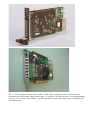
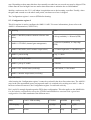
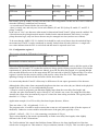
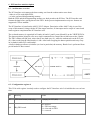
European Synchrotron Radiation Facility
Computing Services - Electronics Group
CS/EL/02-03
C111 / P111 4 channel Time to Digital Converter
User's manual
updated 08/11/07 by C. Hervé
VHDL source revision 2.10 and later.
Table of contents
1 - General description
2 - Specifications
3 - Boot configurations summary
4 - Front panel description
5 - Readout unit description
6 - PCI interface unit and internal memory description
7 - Programming the C111 board
8 - Advanced configurations
9 - GFD commissioning procedure, step by step
10 - GFD note about maximum delay line length
1 - General description
C111 (or P111) is a simple to use yet powerful time to digital converter (TDC) implemented in the
CompactPCI (or PCI) format. Both variants are 100% compatible. In the rest of this document we shall
refer to as C111 but it also applies to the P111 design.
The C111/P111boards are based on the AMS111 ASIC. This component features a 80 ps rms time
resolution with a differential linearity better than 1%, a short 16 ns dead time and a very high throughput
in excess of 107 events/s. The AMS111, input/output buffers and some ancillary logic are mounted on a
mezzanine board.
This mezzanine fits on a CUB (CompactPCI Universal Board, ESRF design) or a (PUB PCI Universal
Board, ESRF design) mother board. It provides a PCI interface (AMCC S5933 chipset), a local storage
memory (256 or 512 MBytes) and a large Field Programmable Gate Array (FPGA) where all C111
functionalities are implemented.
The FPGA may be dynamically reconfigured at any time. At the system boot time a boot configuration is
downloaded by the C111 software driver. Different boot configuration files may be developed to fit
different applications. The following boot configurations are available:
- MHIT: 4 channel multihit with common stop;
- MHIP:4 channel multihit with periodical common start;
- GFD: 4 channel gas filled detector with common start.
The C111 TDC is made of three building blocks: the ASIC/TDC readout unit, the histogramming
memory, and the PCI interface unit. The simplest operation is by reading out the data on the fly from the
PCI bus, not using the histogramming memory. To overcome a possible limitation of the readout speed
because of the software running in the host processor, the on board memory may be used.
The elementary bin time (resolution) is factory set to 150 ps. Alternatively the resolution can be
determined by an external clock.
2 - Specifications
2.1 - Inputs
Number of channels
4
COM, X1, X2, Y1, Y2
fast NIM (0 - 0.8 V), 50 Ohms adapter
ECL option available on request
CLR
Analog discriminator -1 V to +3 V, 50 Ohms adapter
Suitable for fast NIM or TTL like inputs; factory set to 1.5 V
threshold
External clock (optional)
Max. ± 4 V, 50 Ohms adapter, sine or square wave
Input pulse width
5 ns min, falling edge sensitive
Common start to any hit input (GFD,
MHIP)
3 ns min.
Common stop period (MHIT), min.
120 ns
2.2 - Time coding
Resolution
150 ps (bin time), 100 ps (RMS)
Differential non linearity (DNL) ±1%
Dynamic range
14 bits (about 2.4 us)
Dead time (GFD)
30 ns
Dead time (multihit, multihip)
16 ns two first hits, then 40 ns typical depending on event statistics
2.3 - Readout throughput
2D-GFD, gate length 150 ns
4 106events/s max.
Multihit
2.5 MHz max. stop frequency
Multihip
6.0 MHz max. start frequency
Local memory histogramming rate
7 106events/s
Local memory initialization rate
320 Mbytes/s
Local memory size
2 banks of 128Mbytes or 256Mbytes
2.4 - Gating and event time stamping
Gate resolution
19.2ns
Gate duration
100 ns to 4 us, programmable
Gate jitter
±5 ns (GFD and MHIP configuration)
Time stamp resolution
76.8 ns
Time stamp range
28 bits (about 5.25 s)
2.5 - PCI interface
Data path
32 bits @ 33 MHz, 5 Volts signalling
Mode
Target read/write
Power supply
5 Volts @ 400 mA, 3.3 Volts @ 200 mA max.
2.6 - Front panel outputs
Monitor signal
slow NIM (+5V)
3 - Boot configurations summary
CUB total memory size may be 256 Mbytes or 512 MBytes. The GFD configuration is memory size
dependant. Others are not.
Name
Short description
The C111 TDC is triggered by any hit on any (0-3) channel.
It waits until the common stop (or time out) pulse has been received.
multihit
Time differences from the common stop are then computed for each channel.
Dead time (defined as two sequential hits on the same channel) is 16 ns maximum.
Memory
256M
or
512M
The C111 TDC is always triggered by a common start pulse. The start signal must be
periodical.
256M
multihi
C111 then records the hits on the four other channels and computes the time difference or
p
from the common start.
512M
Dead time (defined as two sequential hits on the same channel) is 16 ns maximum.
GFD
The C111 TDC is always triggered by a common start pulse.
It then records the hits on the four other channels which are used to compute the X and
Y coordinates of the event originating from the (gas-filled) detector. A built in pile up 256M
detection logic rejects bad events.
Dead time (defined as two sequential, not piled up, events) is 30 ns maximum.
GFD2 Idem above
4 - Front panel description
512M
4.1 - LED indicators
FAIL red
Internal hardware error. Switched on following a
system reset, then normally off after a configuration
file has been downloaded.
amber TDC paused, awaiting software restart
green
C111 is PCI bus master
GATE green
Copy of the MONITOR external output (GATE by
default, see 8.5) (note1)
PUP
Dual purpose: indicates an error (note1) condition or
AMS111 PLL unlocked
red
RDY green
Data ready (note 2)
Note 1: Error meaning depends on the boot configuration, GFD or MultiHit.
GFD: piled up events
MultiHit: Time out (no stop) or start pulse close to stop pulse by less than 10
ns. The latter must be considered as a warning; the event is most often
correctly recorded, but this should be avoided as much as possible. In case of
very high event rate start too close from stop might be lost (more than 10 ns is
safe). In general this can easily be achieved by delaying the common stop as
necessary using a cable.
Note 2: The RDY status is memorized for about 70 ms. Therefore even at very
low event rate this led reliably indicates data delivery. By contrast the GATE
led is NOT memorized. The latter intensity reflects the true event rate and becomes hardly observable
below 100 KHz.
4.2 - Connectors
From top to bottom:
GATE Positive slow NIM out Gate or monitor activity, software programmable (see 8.5)
CLR
NIM, coax
in
Inhibit, fast clear or C216 TFG I/F, software programmable (see 5.4)
COM
NIM, coax
in
Common stop, common start (GFD)
Y2
NIM, coax
in
channel 3, Y2 (GFD)
Y1
NIM, coax
in
channel 2, Y1 (GFD)
X2
NIM, coax
in
channel 1, X2 (GFD)
X1
NIM, coax
in
channel 0, X1 (GFD)
5 - Readout unit description
5.1 - Architecture overview
The readout unit is responsible for the time coding and processing of the raw values before passing the
results onto the PCI bus interface or the histogramming memory. This is implemented partly in the
AMS111 ASIC and partly in the FPGA. This document describes the present functionalities of the C111
board. New functionalities could be developed upon request by modifying the FPGA boot program.
In case the on-board histogramming memory is not used the host processor software somewhat paces the
actual readout speed. Should the PCI interface becomes slower than the arrival of events, the readout unit
will pause. During that period new incoming events are lost. Typically a readout throughput of 200
Kevents/s can be achieved safely by most readily available processors. This includes basic processing like
sorting the data to build up a histogram in the host memory. When the on board histogramming memory
is used, events readout proceed at full speed (up to 5 Mevents/s sustained).
Next paragraphs describe the resources that are involved in the readout procedure.
5.2 - Boot configurations
5.2.1 - Multihit boot configuration
The C111 always operates in the "common stop" configuration whereby the COM signal terminates an
acquisition sequence. Any hit on whatever channel 0 to 3 wakes up the TDC. Hits are recorded until a
common stop pulse arises.
- Time coding is done on the fly by latching the status of a free running counter with a bin time of 150 ps.
This yields some values: Z (COM stop) and Yn (hit on channel n, n from 0 to 3).
- Data are extracted from the ASIC and fed to an arithmetic unit which computes the differences:
Xn = Yn - Z, for each hit on each channel.
- Several hits can be recorded on the same channel, before the common stop arises. Then several Xn
values are produced related to the same channel number.
- In case the common stop pulse is missing, a time-out is triggered. Already recorded hits are flushed out,
and a new sequence may restart.
Typical output rate is 10 MHz, but strongly depend on the input statistics and the common stop period.
5.2.2 - Gas-filled detector boot configuration
The C111 always operates in the "common start" configuration whereby the COM signal initiates an
acquisition sequence.
- An internal gate is generated. Its duration is determined by the time-out register value.
- Time coding is done on the fly by latching the status of a free running counter with a bin time of 150 ps.
This yields 5 values: Z (COM start), X1, X2, Y1 and Y2.
- Data are extracted from the ASIC and fed to an arithmetic unit which computes the results.
X = X1 - X2 + OffsetX
Y = Y1 - Y2 + OffsetY
(the offset is discussed below; Z value is not used, but in the test mode described later on)
- The X and Y results are latched as a single word and are simultaneously available to the PCI interface
unit.
- A built in pile up detection logic rejects bad events.
The peak output rate is 4 MHz (assuming a 150 ns gate length).
Event time stamping is available when reading out data on the fly through the PCI bus (not using the
build in histogramming memory).
5.2.3 - Multihit boot configuration
The C111 always operates in the "common start" configuration whereby the COM signal initiates an
acquisition sequence.
- An internal gate is generated. Its duration is determined by the time-out register value.
- Time coding is done on the fly by latching the status of a free running counter with a bin time of 150 ps.
This yields some values: Z (COM stop) and Yn (hit on channel n, n from 0 to 3).
- Data are extracted from the ASIC and fed to an arithmetic unit which computes the differences:
Xn = Yn - Z, for each hit on each channel.
- Several hits can be recorded on the same channel during the gate duration. Then several Xn values are
produced related to the same channel number.
Typical output rate is 25 MHz, but strongly depend on the input statistics and the common start period.
5.3 - Timer
The timer is most often used to control the statistics registers (see 6.6). It may also be used as a general
purpose timer, for example, to control the acquisition duration. The timer is 24 bit wide. This timer should
neither be confused with the time-out counter (see 5.4, next) nor the time stamp counter (see 6.4). The
timer is no way linked to the hardware acquisition process.
Writing in the timer register set the timer load value. The timer is reloaded during the clear/pause TDC
command. When clear/pause is released the timer counts down. When it reaches zero, an interrupt is
generated and counting stops. Then the timer interrupt is inhibited until a clear command (see 6.2)
resumes its usage. If the timer is not used its interrupt must be masked off (see 6.2). Reading out the timer
register yields the present counter value. To read back the timer load value, pause the C111 (this reloads
the counter and keeps it idling), then read out the timer register.
The timer clock is derived from the PCI 33 MHz clock by the following formula.
Timer clock = 33.33 / 2**21 MHz
So, approximately, Timer period = 62921 us
5.4 - Configuration register 1
This 16 bit wide register is mainly used to configure the operating mode of the C111 TDC. The C111 can
be operated in "normal" or "test" modes. Thereafter we only consider the "normal" case. Test modes are
addressed in chapter 8.
The upper byte is the load value for the time-out counter. This 8 bit time-out value determines the internal
gate (2D) or common stop watch-dog (multihit) duration.
The LSB value depends on the time resolution according to the formula:
Time-out LSB = 128 * Resolution
hence, at 150 ps resolution,
Time-out LSB = 19.2 ns
The time-out duration is related to N (N>0), the time-out register contents, by the following formula:
Multihit:
Time-out (ns) = 40 + N * LSB
Multihip:
Time-out (ns) = 100 + N * LSB
GFD:
Time-out (ns) = 80 + N * LSB
bit
Meaning
Value
3-0
Mode select
0000 = GFD readout, two-D, external inhibit
0001 = GFD readout, one-D, external inhibit
0010 = GFD readout, two-D, external fast clear
0011 = GFD readout, one-D, external fast clear
0100 = multihit, external inhibit
0110 = multihit, external inhibit, burst skipping
1000 = multihip, external inhibit
4
Mode type
0= Normal, 1= Test
5
Mode Acknowledge (read only)
0= OK, 1= unknown
Front panel MONitor output select
00= Gate
01= Clear Error (ALU processing done, MHIP only)
10= ALU overflow (GFD only)
11= AMS111 monitor
7-6
15-8 Time-out
1-255
After programming the mode the configuration register 1 should be read back to check the Acknowledge
bit. A given boot configuration file may not implement all operating modes. In the future, new operating
modes could be implemented and selected using the reserved bits. Verifying that the Acknowledge bit has
been cleared makes sure that the requested mode is actually supported in this particular C111 TDC.
GFD 1D readout note : bit 0 selects between one- or two-dimensional detector type. In one-D, the signals
are collected from the X1 and X2 inputs. The Y resulting values are forced to zero. In one-D, it is
mandatory to clear the Pileup Y enable bit in the Configuration register 2, otherwise all events would be
rejected.
GFD front panel CLR input note : bit 1 selects between two styles regarding the front panel "CLR" input.
"Inhibit" means that the "CLR" input is level sensitive. When high the C111 does not record any event.
"Fast clear" means that the "CLR" input is falling edge sensitive. This edge is only detected during the
GATE activity (after a common start has triggered event acquisition). When "Fast clear" is activated it
cancels the record of the one event being processed. Then the acquisition resumes. It is intended, for
example, to discard events based on energy resolving. In MHIT configuration the external CLR is always
treated as an inhibit signal.
Should the "time resolved" mode be selected (see 5.7), then the CLR input is dedicated to receive the
FCTRL2 output from the C216 Time Frame Generator board. In the later case configuration register bit 1
is ignored.
Multihit readout note: bit 1 enables burst (from stop to stop) skipping. In skipping mode C111 gets hits
until the common stop occurence; then hits are masked (and the C111 is read out) until the next common
stop. Depending on how many hits have been actually recorded one our several stop may be skipped. This
feature must be used at high event rate and/or short burst time to minimize the overall deadtime.
Multihip readout note: the C111 self-adapts it acquisition rate to the incoming event flux. Usually, when
the gate lenth extends over the whole start period, one burst out of two is skipped.
The Configuration register 1 resets to $FF00 after booting.
5.5 - Configuration register 2
This 8 bit register is used to configure the AMS111 ASIC. For more informations, please refer to the
AMS111 documentation (CS/EL/02-01).
bit Meaning
0
Value
AMS111 MASK4 (readout common reference time
value)
0= Keep (multihit), 1= Discard (GFD)
1 AMS111 STYLE03 (internal gate management)
1= Gate level (multihit), 0= Stop edge
(GFD)
2 AMS111 MUXSEL (ASIC monitor output select)
0= Counter highest bit, 1= MASK4 copy
3 AMS111 power saving
0= up, 1= down
4 AMS111 pile up X enable
0= Disable
5 AMS111 pile up Y enable
0= Disable
6 AMS111 PLL locked status (read only)
0= OK locked, 1= Not locked
7 AMS111 Monitor output status (read only)
Important notes:
After booting, the Configuration register 2 cannot be read until it has been first written into. The AMS111
stays in the (non operational) power saving mode until it is switched on by writing zero in bit 3. After it
has been written at least once, the Configuration register 2 reads back correctly.
Bit 1 (style03) strongly depends upon the FPGA boot configuration. This also applies to the MASK4 bit.
It is the software responsibility to keep the STYLE03 and MASK4 bits consistent with a given boot
configuration. Next table summarizes the different cases.
Mode
Conf. 1 LSB encoding
STYLE03
MASK4
boot config.
GFD imaging
0000X
stop edge
discard
2 (gfd)
multihit
00100
gate
keep
1 (mhit)
mutihip
01000
stop edge
keep
3 (mhip)
GFD sum
1000X
stop edge
keep
2 (gfd)
raw
10100
gate
discard
1 (mhit)
Bits 4 and 5 (pile up enable) are only relevant in the GFD configuration. In this case an event is valid only
when the following conditions have been met:
- no second start is detected before the end of the gate;
- there is exactly one, and only one, hit on each channel (X1 and X2 if pileup X enable, Y1 and Y2 if
pileup Y enable).
In the case of "true" area detectors (that means bi-dimensional) both X and Y pileup must be enabled. For
a linear detector the pileup detection must be disabled on the unused channels. Since there is a single
pileup detection logic, only one linear detector may be managed at a time (and not two of them).
To be sure that the AMS111 PLL is locked, bit 6 should be read several times since the unlocked flag is
not memorized. The PLL can be considered as actually locked when all reads yield zero. A single non
zero value indicates that the PLL is not locked and this must be reported as an error.
5.6 - Configuration register 3
This is only relevant in GFD mode of operation.
bit 19-18
bits 17-10
bits 9-0
quarter/half resolution (when set)
Offset X
Offset Y
There are separate offset registers for the X and Y channels. The offsets are used to shift the results of the
subtractions X1-X2 and Y1-Y2 so that the results are always positive binary encoded values. This fits the
requirement of a delay line based detector. Indeed, given DL the delay line length, it is expected that the
time encoded differences are in the range minus DL (left end side) to plus DL (right end side). The offset
register is used to bias the result to always yield positive values from 0 to 2 DL. This simplifies the
updating of images in the back-end electronics and/or host software.
It is noteworthy that the X and Y offsets may be different to fit non square geometries of the detector.
Although the offset value often conceptually duplicates the time-out value (they are linked to the physical
length of the lelay lines), it is set independently because
- it may be secure to program a gate duration slightly larger than the exact delay line length, and,
- the time out value increments by steps of about 19.2 ns, which is too coarse for setting the offset bias.
Actually the offset value increments by steps of 16 times the time coding resolution. The typical pitch is
therefore 16 * 150 ps = 2.4 ns.
Application example, for a 250 ns delay line based square detector, follows.
Time-out value = 250 - 80 (pedestal) / 19.2 = 9
The program value 10 could be used to ensure that events are well captured (trade off at the expense of
dead time). Otherwise events could be missed because of the gate jitter (typically ±5 ns).
OffsetX = OffsetY = 250 / 2.4 = 104 (assuming a resolution of 150 ps)
These values should be fine tuned experimentally to fit the exact delay line lengths, often slightly
different in the X and Y dimensions.
The "half resolution" bit controls the final data format. When set, the least significant bit of the time
coded value is stripped out. This mimics a 300 ps resolution (instead of 150 ps). This is useful to pack the
data in the local storage memory when the full resolution is not required.
Configuration register 3 resets to zero after booting.
5.7 - Configuration register 5
This is only relevant in GFD mode of operation when the C216 TFG is used to control the C111 TDC.
Configuration register 5 controls the storage memory mapping.
bit
Meaning
Value
Memory mapping mode
0000 = no time resolved, 4K*4K
0001 = time resolved, no ROI
0011 = time resolved, ROI size 512*512
(NIYet)
7-4
Image size (time resolved, no ROI)
0000 = 1D or 4K*4K
0001 = 512*512
0010 = 1K*1K
0011 = 2K*2K
11-8
ROI X origin
256 pixels increment
15-12 ROI Y origin
256 pixels increment
3-0
27-16
Current live frame number (time
resolved)
Read only
Next table summarizes the maximum number of frames, depending on the CUB memory and image sizes.
Image (32 bit
pixel)
CUB 256M CUB 512M
512*512
128
256
1K*1K
32
64
2K*2K
8
16
4K*4K
1 (note)
1 (note)
1D
4K
4K
Note: Indeed time resolved is not supported for those large images, as it would make little sense.
5.8 - Test register
This register is not used in normal operation. It may be used to check the C111 hardware. This is
addressed in chapter 8.
6 - PCI interface unit description
6.1 - Architecture overview
The PCI interface unit captures the data coming out from the readout unit to store them
- either in a 256 word depth FIFO,
- or in the on-board histogramming memory.
Both the FIFO and the histogramming memory are dual ported to the PCI bus. The PCI interface unit
formats the data before storing them in the FIFO. In the present implementation only two formats are
supported: GFD or multihit.
The PCI interface is based on the AMCC S5933 chipset. Description of the AMCC chip is out of the
scope of this manual. Along with the PCI bus target interface, an interrupter and a couple of control and
status registers complement the PCI interface unit.
The on board memory is organized in 2 banks (#0 and #1) and 2 ports (M and P) on the VIRTEX FPGA.
The data acquisition principle relies on a single command bit to control the switch between the 2 banks.
The TDC readout unit (M port) writes data to one bank (say #1), while the readout task on the PCI port
(P), either reads from the other bank or is idle. After bank swapping the data acquisition task may carry
on on bank#0 while PCI reads bank#1.
A built-in hardware allows to initialize (to clear in particular) the memory. Bank clear is performed from
port M under PCIbus control.
6.2 - Configuration register 4
This 32 bit wide register is mainly used to configure the PCI interface unit. It is initialized to zero at boot
time.
bit
Meaning
Value
0-7
FIFO word count (read only)
0 (empty) to 255 (full)
IRQ FIFO mask
00= masked
01= FIFO not empty
10= 64 words in FIFO
11= reserved
9-8
10
IRQ timer mask
0= masked
11
timer status (read only)
1= counting
12
statistics overflow status (read only) 1= overflow
13
IRQ timer status (read only)
1= pending
14
IRQ FIFO status (read only)
1= pending
15
IRQ pending (read only)
1= pending
16
FIFO enable
1= enable FIFO, 0= enable local SDRAM
17
CLR front panel input status
Active High
18-27 Reserved
30-28 Statistics channel selector
0-6
31
0= acquisition start, 1= TDC clear and acquisition stopped
clear (and pause) TDC
Writing a one in bit 31 does a "clear TDC" command. It re-initializes the readout unit. It does not touch
any register but the FIFO word count (see 6.4, next) and the statistics registers (see 6.5), which are
cleared. Then the C111 TDC pauses. Writing zero in bit 31 resumes the acquisition. Following a system
reset, the clear bit is set and the acquisition is therefore paused.
When not using the FIFO must be disabled. This prevents the acquisition into the local memory to stop
because the FIFO would overflow, in which case no data would be made available anymore. When
initializing the memory contents (see 6.3.5), the FIFO must be enabled.
Either of timer terminal count reached or statistics register overflow condition generates the so called
"timer interrupt". Reading out the configuration register 4 clears the timer interrupt. Then the timer
interrupt is inhibited until a new "clear TDC" command resumes its usage.
6.3 - CUB registers
6.3.1 - CUB control register
bit
Meaning
Value
31
Software reset (write only)
1= reset
30
SDRAM bank select
1: P->BANK#1, M->BANK#0
0: P->BANK#0, M->BANK#1
29-0
SDRAM configuration
Expert reserved
Writing one at bit 31 makes a global reset (but the FPGA is still booted and operational). It is not
necessary to clear the software reset bit. Under regular usage, this reset feature should not be required.
After a software reset, all registers are back initialized to the boot default values. The SDRAM
configuration bits are initialized during the boot. They should not be changed then.
To swap memory banks, write the SDRAM bank select as required. The actual change of banks my be
delayed by a dew hundreds nanoseconds (and never more than 7 us). Before starting any SDRAM access
to the new bank, the software must check the "SDRAM bank status" bit to guarantee data integrity (see
6.3.4).
6.3.2 - CUB status register
bit
Meaning
Value
0
power 1.8V
1 = OK
1
power 2.5V
1 = OK
2
power 3.3V
1 = OK
3
power 5V
1 = OK
4
power +12V
1 = OK
5
power -12V
1 = OK
7-6
Reserved
0
9-8
Reserved
1
10
33 MHz PLL locked
1 = OK
11
TDC clock PLL locked
1 = OK
23-12
Reserved
0
31-24
CUB serial number
The CUB status register is read only.
6.3.3 - CUB temperature register (NIYet)
bit
Meaning
Value
6.3.4 - CUB SDRAM register
bit
Meaning
Value
31
SDRAM bank status
30
SDRAM FIFO status
29-0
SDRAM configuration
1= P->BANK#1, M->BANK#0
0= P->BANK#0, M->BANK#1
Expert reserved
The SDRAM configuration bits are initialized during the boot. They should not be changed then.
6.3.5 - CUB SDRAM CLEAR register
bit
Meaning
Value
0
Start initialization (W only)
1= start
1
Pattern increment (R/W)
1= increment
2-29
reserved
0
30
Initialization done
1= in progress
31
Initialization request status
bit 0 copy;
needs to be cleared before new request
To clear the memory, a zero value pattern (see 6.3.8) without increment does the job. The increment
feature may be used for test purpose: the value written to the memory is incremented along with the
address. Before starting the initialization sequence, the histogrammer must be stopped. This is done by
enabling the readout FIFO, which can be symmetrically understood as stopping the histogrammer (set
configuration register4, bit 16). The whole procedure is done when bit 31 is one and bit 30 is zero.
Typical initialization speed is 400 Mbytes/s.
The initialization sequencer only runs at memory port M. Depending on which bank needs to be cleared,
the consistent bank swap selection must be implemented before.
6.3.6 - CUB SDRAM START register
Start address pointer; rounded at 8 words boundary.
6.3.7 - CUB SDRAM END register
End address pointer; rounded at 8 words boundary. The initialization includes the 8 end address locations.
That means, for example, to stop at 0xc00 set end register at 0xbff (0xbfc does the same).
6.3.8 - CUB SDRAM PATTERN register
The value to be written into the memory. This may be incremented at each location if the "increment" bit
is set (see 6.3.5).
6.4 - FIFO to PCI bus
The FIFO for data storage to PCI bus is 256 word depth. It can only be readout from the PCI bus by 32 bit
wide words. For test purpose the FIFO can also be written into (see 8.1). Data are presented onto the PCI
bus by reading a single 32 bit wide location called the "FIFO data register". Closely coupled with the
FIFO management is the configuration register 4 that keeps track of the number of data words already
stored in the FIFO memory.
The PCI interrupter is triggered by the number of data already stored in the FIFO. Depending on bit 9-8
of the configuration register 4 an interrupt may be generated when the FIFO is not empty or at least 64
words have been filled in. The PCI interrupt request is cleared after the FIFO is empty (that is after all
data have been read out).
Depending on the configuration the data storage is organized differently. In GFD configuration not only
the event (X-Y coordinates) is recorded, but in addition each event is preceded by a time stamp value.
Thus in GFD configuration for each incomming event 2 words are sequentially stored in the FIFO: first
the time stamp, then the X-Y coordinates.
Depending on the operating mode, the 32 bit data word is formatted as follows.
Multihit and multihip data format
31-16
15-14
13-0
0
Channel (0-3)
Time (from stop) value
GFD 1D data format
31-14
13-0
all zero
X value
GFD 2D data format
31-24
23-12
11-0
all zero
Y value
X value
Note1: in GFD 2D-format, should a result overflow the 12 bit range, it is discarded.
GFD time stamp format
31-28
27-0
1000
time stamp value
It may exceptionally happen that there is no actual X/Y data following a valid time stamp, in particular
when an overflow has been detected.
The time stamp period is 4 times the main TDC clock period.
Hence, at 150 ps resolution:
Time stamp period = 76.8 ns
6.5 - Local memory mapping
6.5.1 - Local memory addressing
The C111 local memory is always managed by 32 bit words. From port M, the memory is always used in
the histogramming mode. That is every event increments a single location. The memory address being
incremented is directly determined by the pixel data format as described in the previous section (FIFO to
PCIbus). This is described in the next table.
Configuration
Addressing
Address range
MHIT or MHIP
pixel data * 4
0 - 0x03FFFC
GFD 1D
pixel data * 4
0 - 0x00FFFC
GFD 2D, NOT time
resolved
pixel data * 4
0 - 0xFFFFFC
(fixed 4K*4K image size)
Image Size
GFD 2D, time resolved
512
LSBits: pixel data * 4
MSBits: according to conf. reg.
1K
5
2K
Frame number
(CUB memory 512M assumed)
256
64
16
6.5.2 - Bank swapping
It is up to the host computer to manage memory banks swapping at his best convenience. Basically 2
strategies may be implemented.
Single bank acquisition scheme
Select bank 0 (this means: bank 0 to PCI, bank 1 for acquisition). Clear memory (bank 1). Start
acquisition. Stop acquisition.
Select bank 1 (this means: bank 1 to PCI). Host readout via PCIbus (whilst acquisition is stopped). Restart
select bank 0 ...
Bank 0/1 could be permuted without affecting the strategy.
Dual bank acquisition scheme
Select bank 1 (this means: bank 0 to PCI, bank 1 for acquisition). Clear memory (bank 0).
Select bank 0 (this means: bank 0 to PCI, bank 1 for acquisition). Clear memory (bank 1).
Start acquisition.
Select bank 1 (this means: bank 1 to PCI, bank 0 for acquisition). Host readout via PCIbus. Acquisition
continues in bank 0.
Select bank 0 (this means: bank 0 to PCI, bank 1 for acquisition). Host readout via PCIbus. Acquisition
continues in bank 1.
Host processor merges bank 0 and 1 contents (for monitoring purpose); and so on...
Stop acquisition and flush out last bank used to complete data acquisition.
6.6 - Statistics registers
The statistics registers aim at monitoring the event rate. Depending on the boot configuration, different
statistics registers are available. Statistics operation is closely related to the general purpose timer.
Multihit data format
There are 5 statistics registers.
The first four (indirect address 0 to 3) are each related to one channel. All operate the same way.
- The statistics register is cleared by the clear command (and the timer is reloaded).
- After pause has been released, the hits (for each channel separately) are counted up (and the timer
counts down).
- When the timer stops, statistics are frozen and an interrupt is generated.
The 5th register (indirect address 4) records lost hits. These could be captured but couldn't be safely
related to a definite stop and have been discarded. It is noteworthy that even more hits (than recorded)
may have been lost, some of them just not captured at all due to the input deadtime.
The statistics registers are 28 bit wide. In the case any statistics register would get its MSbit set, this is
flagged as "statistics overflow" and and interrupt is generated.
The statistics registers can be read out from the PCI bus through indirect addressing. The statistics register
number to be read out must first be written into the configuration register 4. Then the contents of the so
specified register may be read out from the (shared) statistics register location.
Multihip data format
The statistics operate the same as in the multihit configuration, but the 5th register (indirect address 4)
records common start hits (those not skipped by the C111 logic).
GFD data format
The same 5 registers as above (multihip) are available (indirect address 0 to 4). In addition there are 2
more statistics registers:
- Rejected (pileup) event count (indirect address 5);
- ALU overflow (indirect address 6).
It must be further commented that there are
- the real start pulses, all those produced by the detector system;
- the detected start pulses, which are slightly less since at times the C111 board may be still busy
processing the previous event; Those are accumulated in the statistics register 4;
- the accepted start pulses, which in 2D mode is even less because of the pile up rejection logic.
The statistics register may be used to compute
- the data rate of the seen events;
- the ratio accepted versus seen events;
- the balance X1, X2, Y1, Y2 ...
7 - Programming the C111 board
7.1 - Plug & play
Vendor Id: 10E8 (AMCC)
Device Id: EE08 (ESRF/C111)
7.2 - Address map and registers summary
CUB general purpose registers are mapped in IO segment 1.
Offset
Type
Name
Description
0x00
W once
CUB control
6.3
0x04
W once
CUB SDRAM control
6.3
0x08
R
CUB status
6.3
0x0C
R
Temperature status
6.3
0x40
R/W
SRDAM clear
6.3
0x44
R/W
SDRAM start
6.3
0x48
R/W
SDRAM end
6.3
0x4C
R/W
SDRAM pattern
6.3
C111 dedicated registers are mapped in IO segment 2.
Offset
Type
Name
Description
0x00
R
data FIFO port
6.4
0x04
R/W
Configuration 1
5.4
0x08
R/W
Configuration 2
5.5
0x0C
R/W
Configuration 3
5.6
0x10
R/W
Configuration 4
6.2
0x14
R/W
Configuration 5
5.7
0x18-0x30
Reserved
0x34
R/W
Timer
5.3
0x38
R
Statistics
6.6
0x3C
W
Test pattern
8.1
Memory bank 0 (respectively 1) is mapped in memory segment 3 (respectively 4).
7.3 - Software
7.3.1 - Basic utilities
The Electronics Group has developed several basic utilities (running under the LINUX and WINDOS
operating system).
- c111tst: general purpose test and C111 handling program.
- c111plot: a simplistic acquisition software.
- c111magic: heuristic tuning of the C111 board for the readout of a 2D-GFDdetector.
7.3.2 - GUIs
The Electronics Group has developed Graphical User Interfaces (only validated in the WINDOWS
environment).
C111gui-1D is dealing with MHIT, MHIP and GFD-1D, whereas C111gui-2D is dealing with GFD-2D.
8 - Advanced configurations
8.1 - C111 test mode: hardware check
The 32 bit test register can be used to check the C111 hardware. Writing in the test register mimics the
AMS111 output port according to the following format.
31-30
29-16
15-14
13-0
Y port status
Y data
X port status
X data
Then the storage memory can be read back to verify that the data path looks fine. This specific test mode
is available in the MHIT configuration only.
The AMS111 ASIC can be further tested by exercising the MASK4 bit of its control register (see 5.5).
A simplified test procedure for the AMS111 ASIC may involve the following steps, using the
configuration register 2.
- Reset state, PWD=1; check that LOCK remains low (PLL is locked).
- Set PWD=0;Power is now up; check PLL still locked.
- Set MUXSEL to 1; switch MASK4 on and off; MONITOR output follows the MASK4 internal bit
status. This further tests the serial connection to the ASIC.
8.2 - C111 test mode: raw time coding readout
config. #1 bits 4-0
10100
This feature is only available in the multihit boot configuration. In this configuration raw time coded
values on channel 0-3 are presented at the output of the readout unit (instead of the computed
differences). This may be used to check the differential non linearity.
8.3 - GFD detector test mode: sum readout
config. #1 bits 4-0
10000
This feature is only available in the GFD boot configuration. Configuration register 2 should be 0x34 or
so depending on desired pile up selection. It is noteworthy that configuration register 2 bit 0 must be zero,
so as the common start time stamp (Z) is kept. Offsets (configuration register 3) are not used.
In this configuration C111 computes (with the notation of 5.2) the values
X = X1 + X2 - 2*Z
Y = Y1 + Y2 - 2*Z
The sum readout is very convenient to tune a delay line based detector. Ideally the X and Y values should
be invariant and equal to the delay line lengths. A histogram of the results is expected to give one peak
above a flat and very low background. The position of the maximum of the peak yields the delay line
length. The sharper and more symmetrical, the better is the detector. An important background noise
indicates a detector with poor resolution.
8.4 - Controlling the resolution
Because of aging or under stressing temperature conditions it might exceptionally happen that ASIC
cannot lock at the imposed resolution. The LOCKED bit should be carefully checked (see 5.5). Also
when the PUP LED on the front panel flickers in the absence of external hits (with the cables
disconnected) this indicates that the PLL is not locked, which spoils the resolution.
The elementary bin time coding can be controlled from an external clock. In this case
- an hardware switch needs to be configured, and a clock supplied on the internal SMB connector;
- analog control of the AMS111 ASIC must be retuned in the laboratory;
- the elementary bin size is related to the external clock frequency by the formula:
F(MHz) = 10**6 / Tres(ps) * 256
For example, to get a 150 ps bin size, the external clock frequency is 26.0417 MHz.
The absolute maximum range is 140 to 160 ps.
The external clock input is AC coupled.
8.5 - Hardware monitoring of the C111 activity
One hardware output is available for monitoring purposes on the front panel on coax connector. The
monitor signal may be routed to the front panel under program control (see 5.4 and 5.5) by selecting one
internal signal (from the AMS111 ASIC and from the FPGA). Routing capabilities are summarized in the
next table.
CFG1 bit 7-6
GFD
MHIT
00
GATE
GATE
01
ErrorClear
ErrorClear
10
ALU overflow
AMS111 lock
11
AMS111 monitor
AMS111 monitor
- GATE: actual AMS111 activity from common start to end (GFD) or any hit to common stop (multihit).
It is noteworthy taht the GATE green led will follow the signal selected for monitoring at the GATE
output.
- ErrorClear: actually this is the internal flush signal which is routed there. But since, when piled up
events are detected (GFD mode) the C111 is automatically flushed, this may be used to monitor the level
of pile up (GFD only).
- AMS111 locked: low is OK.
- AMS111 monitor: MASK4 or counter MSB. When counter MSB should be jitter free when the PLL is
locked. The period is 16384 * Tres, typically 2.4576 us.
8.6 - Frame sequencing (time resolved acquisition)
When configured for time resolved acquisition, the CLR front panel input is reconfigured to receive the
framing information. the CLR input is coded in length.
if CLR High ~= 50 ns this is "frame zero" (restart from storage address zero)
if CLR High >= 100 ns this is "next live frame".
if CLR Low this is "dead frame" (events are discarded).
A "frame zero" mark in itself does not actually start the acquisition (a "dead frame" may follow). For the
acquisition to be immediately effective, "frame zero" mark must be followed by a "next live frame", So
typically:
CLR low, High for 50 ns, Low for 50 ns => "frame zero"
CLR High for > 100 ns , Low for > 100 ns => "1st live frame"
CLR High for > 100 ns , Low for > 100 ns => "next live frame"
...
loop back to "frame zero".
9 - GFD commissioning procedure (step by step)
This is an example on how to operate C111 with a usual 2D gas-filled detector.
1) Detector/Discriminators preliminary check
Make sure you get correct fast NIM pulses from the anode (COM C111 input) and the cathodes (X1, X2,
Y1, Y2). C111 has internal 50 Ohms adapters; 0 Volt at rest, measurement on falling (negative voltage)
edge. Minimum pulse width is 5 ns; usual pulse width is 10 to 20 ns. Minimum COMmon start (anode) to
any cathode is 3 ns. A 1 meter long cable does the job, otherwise a few events will be lost (rejected by the
pile-up detection logic).
2) C111 preliminary check
Red led FAIL on: has the software driver actually downloaded a configuration file?
Reboot and check the logical (operating system dependent) devices. If it persists, C111 fails.
After booting, C111 enters a power saving sequence and is not operational yet, but pauses. To wake up
the C111 TDC you must reset bit 3 in the configuration register 2. If the red led PUP remains on (all
inputs being otherwise disconnected), the clock PLL does not lock. If it persists, C111 fails. PUP led is
normally off. FAIL led should be amber (TDC paused).
3) Set up GFD operating mode
Config. register1 LSB=0; check the acknowledge bit has been cleared. If the acknowledge bit in one, then
a wrong configuration file has been downloaded.
4) Set the gate length and start C111
GATE (Config. register1 MSB) = delay line length (in 19.2 ns units minus 80 ns bias, see 5.4).
Connect the anode to the COM input.
Start C111: Config. register4 bit 31 = 0 (un-pause); bit 16 = 0 (prevent FIFO full that would block the
TDC); FAIL led should quit the amber color.
Observe the green led GATE. It is on when anode pulses are detected. Since this is proportional to the
actual event rate, this can be hardly seen below 100K events/s.
Monitor (oscilloscope) the GATE OUT signal (active low), triggered by COM, duration as programmed.
5) Disable the pile up rejection logic
For troubleshooting, expert users may skip that.
Config. register2 = 0x05 .
6) Check (again) the cathodes
Make sure (oscilloscope) you get X1, X2, Y1, Y2 during the GATE activity. Connect them to C111.
Observe the green led RDY. It is on when events have been recorded. This one is memorized (and
therefore mostly independent of the actual event rate) so that it should be visible even at low counting
rate.
7) Activate the pile up rejection logic
Config. register2 = 0x35.
Now the red led PUP flags the rejected events.
Green led GATE continues has before.
Green led RDY should continue almost has before, but in the case most events are being reejected.
For an accurate monitoring of the pile up rejection you may use the statistics registers.
8) Set up the offset registers
Depending on your acquisition system you may use (or not) the offset values from the config. register3.
When used, fine tuning is necessary with the acquisition software in operation.
9) Use our favorite acquisition software
It does not work. It is clearly (!?) a software issue. Call the Expert(s).
It works. Congratulations!
10) Beam lost
That's life.
Back to home or next step.
11) Is the detector (so) good?
A nice feature of C111 is the sum recording mode of operation (see 8.3).
You should observe peaks (one for X, one for Y), the position of which is a measurement of the delay line
length. The sharper and more symmetrical the best. You don't get anything: did you used a Fe source in
replacement of the (lost) beam?
10 - GFD note about maximum delay line length
Let's have D1 and D2 the delays towards both ends of the delay line.
By construction of the detector D1 + D2 = D, the delay line length.
Now let's follow the C111 processing step by step.
- Two measurements are taken from an arbitrary origin (a free running clock). This yields to (with above
notation)
N1 = A + D1
N2 = A + D2 (A is the unknown origin).
- Then the difference is processed:
Na = N2 - N1 = D2 -D1 (this eliminates A).
At this stage
-D < Na < +D (remember, D is the delay line length)
- Finally to avoid negative number the result is biased by adding D. Naming Nb the final result:
0 < Nb < 2*D
The D value is actually taken from the offset registers and may differ in the X and Y directions.
For example, assuming a 250 ns delay line at 150 ps (full) resolution, the expected data range is
500 ns / 0.15 ns = 3333, already quite a large size in 2D!
Next table summarizes the maximum manageable delay line length.
GFD 2D
GFD 1D
full res. @ 150 ps
300 ns
1/2 res. @ 300 ps
600 ns
1/4 res. @ 600 ps
1200 ns
full res. @ 150 ps
1200 ns
1/2 or 1/4 res.
2400 ns