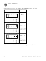
1
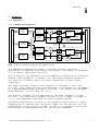
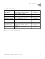
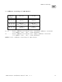
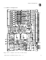
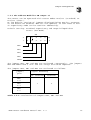
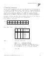
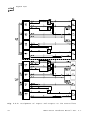
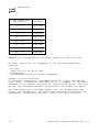
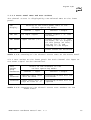
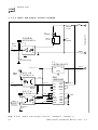
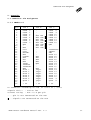
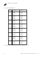
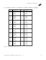
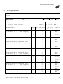
VME - DPIO32
32 digital Inputs or Outputs
Hardware Manual
VME-DPIO32 Hardware Manual Rev. 2.1
N O T E
The information in this document has been carefully checked and is
believed to be entirely reliable. esd makes no warranty of any
kind with regard to the material in this document, and assumes no
responsibility for any errors that may appear in this document.
esd reserves the right to make changes without notice to this, or
any of its products, to improve reliability, performance or
design.
esd assumes no responsibility for the use of any circuitry other
than circuitry which is part of a product of esd gmbh.
esd does not convey to the purchaser of the product described
herein any license under the patent rights of esd gmbh nor the
rights of others.
esd electronic system design gmbh
Vahrenwalder Str. 205
D-30165 Hannover
Germany
Phone: +49-511-372980
FAX:
+49-511-633650
This document shall not be duplicated, nor its contents used
for any purpose, unless express permission has been granted.
Copyright by esd
VME-DPIO32 Hardware Manual Rev. 2.1
Manual File: i:\texte\doku\manuals\vme\dpio32\dpio21h.eng
Described
PCB version
29.07.97
DPI32-5
S/N AB043 and later
Changes in the chapters
The changes in the user’s manual listed below affect changes in
the firmware, as well as changes in the description of the facts
only.
Chapter
2.
Change
Chapter ’Software’ now a separate document.
Further technical changes are subject to change without notice.
VME-DPIO32 Hardware Manual Rev. 2.1
VME-DPIO32 Hardware Manual Rev. 2.1
User’s Manual DPIO32
Content
Page
1. Hardware . . . . . . . . . . . . . . . . . . . . . . . . . .
1.1 Overview . . . . . . . . . . . .
1.1.1 Board Description . . . .
1.1.2 Summary of Technical Data
1.1.3 Software Support . . . .
.
.
.
.
3
3
5
8
. . . . . . . . . . . . . . . . . .
9
1.3 Address Covering of VME-DPIO32 . . . . . . . . . . . .
11
1.4 Jumpers Configuration . . . . . . . . . . . . .
1.4.1 Default Setting . . . . . . . . . . . . .
1.4.2 The Address-Modifier AM Jumper J3 . . . .
1.4.3 Basic Address Decoding via the Jumpers J1
J2 . . . . . . . . . . . . . . . . . . . .
.
.
.
13
14
15
.
19
1.5 Interrupt Processing . . . . . . . . . . . . . . . . .
21
1.6 The Digital Inputs and Outputs . . . . . . . . . .
1.6.1 Controller Assignment to Inputs and Outputs
1.6.2 Pulse Processor HD63143 Structure . . . . .
1.6.3 Input and Output Circuit of DPIO32 . . . .
1.6.3.1 General . . . . . . . . . . . . . .
1.6.3.2 Front Panel LEDs and Test Sockets .
1.6.3.3 Input and Output Circuit Diagram . .
.
.
.
.
.
.
.
23
23
25
27
27
29
30
2. Appendix . . . . . . . . . . . . . . . . . . . . . . . . . .
31
2.1 Connector Pin Assigments . . . . . . . . . . . . . . .
2.1.1 VMEbus P1 . . . . . . . . . . . . . . . . . . .
2.1.2 I/O Connector P2 . . . . . . . . . . . . . . .
2.1.3 Terminal Block I/O Connector P2 Phönix FLKM64
or FLKMS64 . . . . . . . . . . . . . . . . . . .
2.1.4 Description of the Signals at the I/O Connector
P2 (or Terminal Block) . . . . . . . . . . . . .
2.1.5 Wiring Diagrams . . . . . . . . . . . . . . . .
31
31
32
33
. . . . . . . . . . . . . . . . . . . . .
39
2.3 Circuit Diagrams . . . . . . . . . . . . . . . . . . .
41
. . . . . . . . . . . . . . . . . . . . .
43
1.2 Order Information
2.2 Front Panel
2.4 Data Sheets
VME-DPIO32 Hardware Manual Rev. 2.1
.
.
.
.
.
.
.
.
.
.
.
.
.
.
.
.
.
.
.
.
.
.
.
.
.
.
.
.
.
.
.
.
.
.
.
.
.
.
.
.
3
. .
. .
. .
and
. .
.
.
.
.
.
.
.
34
35
1
2
VME-DPIO32 Hardware Manual Rev. 2.1
Overview
1. Hardware
1.1 Overview
1.1.1 Board Description
VME
data bus
driver
MUX
4xOutput
LMD18400
4xInput
electrical
isolation
HD63143
16 Outputs
or
16 Inputs
MUX
CIO Z8536
16 Inputs+
Error Input
4xOutput
LMD18400
Error
VCC
8 groups of each 4 channels
4x
Error
CIO Z8536
16 Inputs+
Error Input
VCC
P2
VME
interrupt
control logic
HD63143
16 Outputs
or
16 Inputs
address, data and control bus
P1 VMEbus
VME address
and
AM decoder
logic
4x
4xInput
Fig. 1.1.1: Block Diagram of VME-DPIO32
The VME board VME-DPIO32 offers a digital process interface
containing 32 optoisolated inputs or outputs. The board is designed
in 6 U format and covers one slot.
The 32 digital I/O channels are arranged in 8 electrically isolated
groups. Each group of 4 channels has the same reference potential.
The user can allocate input or output operation to each group
separately.
The input voltage range of the channels is between 5 V(DC) and
30 V(DC). Each input channel can generate an interrupt on the VMEbus
on a programmable edge (rising or falling). The inputs are voltageproof between -3 V(DC) and +36 V(DC).
The digital outputs can be operated at voltages between 6 V and
28 V(DC). The continuous outputs current at 24 V supply voltage is
0.3 A. The component LMD18400 is used as output driver.
The driver protective circuit is activated at short-circuit, overtemperature or overvoltage. An error signal of the drivers will be
generated at short-circuit to GND, to VCC, at running without load,
overvoltage or overtemperature of the driver component.
VME-DPIO32 Hardware Manual Rev. 2.1
3
Overview
In addition to the bit-programmable operating mode of the outputs,
it is possible to use the single output channels via the pulse
processor components HD63143 for pulse-width modulation (PWM). A
total of 2 x 24 programmable 16 bit registers are available for
switching period and resolution. The minimum switching period
amounts to 10 µs. The outputs can mutually be synchronised.
A total of 20 digital counter inputs of the controllers is
available. At this, four of which are connected in parallel to CIO
8536 and to HD63143. The maximum counter frequency for these four
CIO counters is 3 MHz. Depending on the operating mode, the HD63143
counters can process frequencies from 100 kHz to 1 MHz. For the
counter inputs various operating modes are possible (event counter,
pulse-width measurement, frequency measurement, free running with
interrupt, incremental encoder inputs etc.).
The actual I/O status of the inputs and outputs is displayed on the
front panel of VME-DPIO32 by a two-colored LED for each channel, the
error status is displayed group-wise. Additionally there are test
sockets for each channel located on the front panel for simulation
of the input signals or for disable of the error messages.
4
VME-DPIO32 Hardware Manual Rev. 2.1
Overview
1.1.2 Summary of Technical Data
VME specification
VME interface
IEEE 1014 / D
data transfer mode
SADO24 - slave with A24/D16 access
SD16
- slave with A16/D16 access
address modifier
(AM)
full evaluation of AM0 to AM5,
additionally ’AM2 don’t care’
circuit possible
basic address
selectable by jumpers over the whole
address range of 16 Mbytes
interrupts
I1 to I7 interrupter, level
programmable via HD63143
general data
temperature range
0...70°C
ambient temperature
humidity
max. 90%, non-condensing
connector types
P1-DIN 41612-C96
P2-DIN 41612-C64
board size
160 mm x 233 mm
VME dimensions
6 U height / 1 slot width
weight
ca. 470 g
power supply
VMEbus P1: 5V ± 5%
(typical values at 20 °C):
all outputs OFF:
1.7
all outputs ON:
2.3
16 outputs ON, 16 OFF: 1.7
all outputs OFF,
all inputs ON:
2.3
VME-DPIO32 Hardware Manual Rev. 2.1
A
A
A
A
5
Overview
digital outputs
6
quantity
32 (less inputs)
P-switching:
Out = 24 V --> ’1’
Out = 0 V --> ’0’
supply voltage
Uvccmin
= 6 V (DC)
Uvccmax
= 28 V (DC)
Uvccrated = 24 V (DC)
load capacity
(at 50°C)
rated current/channel (24 V): Ir = 0.3 A
max. current/channel: limited by overtemperature protection (see data sheet
of LMD18400)
max. current/board: 16 A
signal level of outputs at rated
current: ≥ Uvcc-2 V
protective circuits
short-circuit protection and overtemperature protection: electronically
with switch-off of output group,
overvoltage protection (triggering from
Uvcc > 32 V..35 V)
switching
performance
(at 20°)
values for Uvccrated and Ir:
min. pulse time T ≥ 10 µs
min. clock periode TON ≥ 10 µs, TOFF ≥ 10 µs
(With this switching times the signal edges
are bad. Additionally the times may become
longer due to circuit tolerance and ambient
temperature.)
electrical isolation from VMEbus
potential
by optocouplers, acc. to VDE 0110b §8,
isolation class C: 250 V(AC)/300 V(DC)
VME-DPIO32 Hardware Manual Rev. 2.1
Overview
digital inputs (part 1)
quantity
32 (less outputs)
evaluation
all inputs have interrupt capability
max. 16 inputs at P2 configurable as
counter inputs, all 16 inputs
connected to HD63143 and additionally
4 inputs in parallel to CIO Z8536
(higher resolution)
input voltage
permissible input voltage range:
-3 V ≤ Uin ≤ 30 V
Attention: If output driver LMD18400
is supplied by Uvccout,Uin may not
exceed Uin ≤ Uvccout - 2V !
(because of parallel connection to
outputs)
threshold input = ’0’:
Uout ≤ 2.0V
threshold input = ’1’:
Uin ≥ 3.0V
input current
Since the inputs and outputs are
connected in parallel on the board,
the input current depends on the fact,
whether the supply voltage is connected to the output driver LMD18400:
input current/channel at Uvcc = 24 V
(typical values at 20 °C):
input = ’1’: (5 V) Iin = 7.7 mA
(12 V) Iin = 9.9 mA
(22 V) Iin = 10.0 mA
input current/channel at Uvcc not
supplied (typical values at 20 °C):
input = ’1’: (5 V) Iin = 8.0 mA
(12 V) Iin = 14.0 mA
(24 V) Iin = 30.0 mA
(30 V) Iin = 40.0 mA
VME-DPIO32 Hardware Manual Rev. 2.1
7
Overview
digital inputs (part 2)
input frequency
input circuit (max.): 1 MHz
(1:1)
counter frequency of controller
HD63143 (depends on the complexity of
the functions):
just one function:
thigh > 0.5 µs, tlow > 0.5 µs
fmax < 1 MHz (duty cycle 1:1)
16 functions:
thigh > 5.0 µs, tlow > 5.0 µs
fmax < 100 kHz (duty cycle 1:1)
counter frequency of controller
CIO 8536 max. 3 MHz
protective circuit
overvoltage protection by Transsil
diode voltage-proof up to...
statically:
Umax = 36 V
dynamically: Umax = 95 V (duty cycle
1/100, ton = 10 µs)
Umax = 225 V (duty cycle
1/1000, ton = 10 µs)
electrical isolation from VMEbus
potential
by optocouplers, acc. to VDE 0110b §8,
isolation class C: 250 V(AC)/300 V(DC)
Table 1.1.1: Technical Data of VME-DPIO32
1.1.3 Software Support
Driver packages for DPIO32 are available e.g. for operating systems
VxWorks and OS9.
8
VME-DPIO32 Hardware Manual Rev. 2.1
Order Information
1.2 Order Information
Type
Features
Order no.
VME-DPIO32
32 digital inputs/outputs,
PWM, counter, timer
V.1607.02
VME-DIOC-ADAPT1
terminal blocks for P2
V.1601.01
VME-DIOC-ADAPT2
terminal blocks for P2
V.1601.02
VME-DPI32-P2VCC
24 V connection for P2
V.1604.90
VME-DPI32-OS9
C driver for OS-9 as source
code
P.1607.50
VME-DPI32-T
test program PEARL
P.1607.54
VME-DPIO32-MD
additional German user’s
manual
M.1607.20
VME-DPIO32-ME
additional English user’s
manual
M.1607.21
Table 1.2.1: Order Information
VME-DPIO32 Hardware Manual Rev. 2.1
9
10
VME-DPIO32 Hardware Manual Rev. 2.1
Address Covering
1.3 Address Covering of VME-DPIO32
address
range
D15-D8
D7-D0
nn ss FE
nn ss F8
CIO2
(Z8536)
CIO1
(Z8536)
nn ss F6
nn ss F0
RAM of
HD2 (HD63143)
RAM of
HD1 (HD63143)
nn ss DE
nn ss 00
HD2
(HD63143)
HD1
(HD63143)
nn ss ....basic address of DPIO32
via VMEbus (A08 - A23 =
ss .......basic address of DPIO32
via VMEbus (A08 - A15 =
for ’standard address accesses’
CARD-ADDRESS)
for ’short address accesses’
CARD-ADDRESS)
Table 1.3.1: Address Covering of VME-DPIO32
VME-DPIO32 Hardware Manual Rev. 2.1
11
12
VME-DPIO32 Hardware Manual Rev. 2.1
Jumpers Configuration
1.4 Jumpers Configuration
Fig. 1.4.1: Jumpers Position on VME-DPIO32
VME-DPIO32 Hardware Manual Rev. 2.1
13
Jumpers Configuration
1.4.1 Default Setting
The particular factory-settings (of the jumpers see following table)
are marked in the table.
The jumpers configuration can be obtained from the insertion
diagram.
An inserted jumper corresponds to ’0’ (low) level of a signal.
In the following the jumpers are displayed in a position, as seen by
the user, if he has the board lying in front of himself with the
VMEbus connectors to the rear end.
Default jumper setting of jumpers J1 to J4:
jumper
J1
function
setting
basic address
A08-A15
basic address of DPIO32 set
to $xxE14000
J2
basic address
A16-A23
J3
address modifier
AM2 don’t care, i.e. access
in the supervisory mode or
user mode VME access A24/D16
Table 1.4.1: Default Jumper Setting
14
VME-DPIO32 Hardware Manual Rev. 2.1
Jumpers Configuration
1.4.2 The Address-Modifier AM Jumper J3
The DPIO32 can be operated with access modes A24/D16 (standard) or
A16/D16 (short).
At the default setting of jumpers displayed below A24/D16 accesses
to the board are enabled. AM2 will be ignored, so user mode as well
as supervisory mode can be used for addressing.
Default setting: Standard supervisory and nonprivileged data
access (A24-Mode)
J3
2
o
o
o
o
o
10
1
o
o
o
o
o
9
AM0
AM1
AM4
AM2
AM2E
The jumpers AM0, AM1 and AM4 are evaluated ’separately’. The jumpers
AM2 and AM2E form a unit and are always evaluated together.
The jumpers AM0, AM1 and AM4 are evaluated as follows:
jumper/
pins
signal decoding
not inserted
inserted
AM0
1-2
AM1
2-3
1
0
AM4
4-5
Table 1.4.2: Evaluation of Jumpers AM0, AM1 and AM4
VME-DPIO32 Hardware Manual Rev. 2.1
15
Jumpers Configuration
Permissible Positions of Jumpers AM2 and AM2E are as follows:
Position of
jumpers AM2 and AM2E
evaluation
2
4
6
8
10
o
o
o
o
o
o
o
o
o
o
1
3
5
7
A
M
2
9
A
M
2
E
2
4
6
8
10
o
o
o
o
o
o
o
o
o
o
1
3
5
7
A
M
2
9
A
M
2
E
2
4
6
8
10
o
o
o
o
o
o
o
o
o
o
1
3
5
7
A
M
2
9
A
M
2
E
AM2 =
don’t care
AM2 =
1
(supervisory
modes only)
AM2 =
0
(nonprivileged
modes only)
Table 1.4.3: Permissible Positions of Jumpers AM2 and AM2E
16
VME-DPIO32 Hardware Manual Rev. 2.1
Jumpers Configuration
Meaningful address modifier jumpers combinations for 24 accesses are
recommended as follows:
permissible AM codes
jumper J3
A A A A A A
M M M M M M
5 4 3 2 1 0
HEX
addressing mode
2
4
6
8
10
o
o
o
o
o
1 1 1 0 0 1
39
o
o
o
o
o
1 1 1 1 0 1
3D
1
3
5
7
9
2
4
6
8
10
o
o
o
o
o
1 1 1 1 0 1
3D
standard supervisory
data access
1 1 1 0 0 1
39
standard nonprivileged
data access
o
o
o
o
o
1
3
5
7
9
2
4
6
8
10
o
o
o
o
o
o
o
o
o
o
1
3
5
7
9
standard nonprivileged
data access
or
standard supervisory
data access
Table 1.4.4: Recommended Access Modes for Standard Accesses (A24)
VME-DPIO32 Hardware Manual Rev. 2.1
17
Jumpers Configuration
Meaningful address modifier jumpers combinations for 16 accesses are
recommended as follows:
permissible AM codes
jumper J3
A A A A A A
M M M M M M
5 4 3 2 1 0
HEX
addressing mode
2
4
6
8
10
o
o
o
o
o
1 0 1 0 0 1
29
o
o
o
o
o
1 0 1 1 0 1
2D
short nonprivileged access
or
short supervisory
access
1
3
5
7
9
2
4
6
8
10
o
o
o
o
o
1 0 1 1 0 1
2D
short supervisory
access
1 1 1 0 0 1
29
short non-privileged
access
o
o
o
o
o
1
3
5
7
9
2
4
6
8
10
o
o
o
o
o
o
o
o
o
o
1
3
5
7
9
Table 1.4.5: Recommended Access Modes for Short Accesses (A16)
18
VME-DPIO32 Hardware Manual Rev. 2.1
Jumpers Configuration
1.4.3 Basic Address Decoding via the Jumpers J1 and J2
The basic address of VME-DPIO32 is set as follows:
A23..A16 A15..A08 A07..A1
(local address space)
A16 address (J1)
A24 address (J2)
Default setting = $E14000
J2
J1
16
15
16
15
o
o
A23
o
o
A15
o
o
A22
o
o
A14
o
o
A21
o
o
A13
o
o
A20
o
o
A12
o
o
A19
o
o
A11
o
o
A18
o
o
A10
o
o
A17
o
o
A9
o
o
A16
o
o
A8
2
1
2
1
+---short---+
+--------- standard ---------+
An inserted jumper corresponds to the ’low’ level of an address bit.
VME-DPIO32 Hardware Manual Rev. 2.1
19
20
VME-DPIO32 Hardware Manual Rev. 2.1
Interrupt Processing
1.5 Interrupt Processing
The CIO Z8536 components CIO1 and CIO2 can generate an interrupt on
a rising or falling edge of their input signals. The programming of
the CIOs determines, at which edge the interrupt shall be generated.
The two local interrupt requests are combined in the interrupt
logic. If the interrupt enable bit is set, an interrupt can be
generated on the VMEbus, the level of which is freely programmable.
Via port 5 of HD2 (HD63143) the interrupt enable bit is set and the
determination of the interrupt levels vorgenommen:
Local address: $000C HEX
Bit
D7
D6
D5
D4
x
x
x
x
LEV1, LEV2, LEV3:
D3
D2
D0
IREN LEV3 LEV2 LEV1
VMEbus interrupt level:
LEV3 LEV2 LEV1
(D2) (D1) (D0)
0
0
0
1
1
1
1
IREN:
D1
0
1
1
0
0
1
1
1
0
1
0
1
0
1
VMEbus
interrupt
level
IRQ1*
IRQ2*
IRQ3*
IRQ4*
IRQ5*
IRQ6*
IRQ7*
interrupt enable bit:
IREN = ’1’ - interrupt enabled
IREN = ’0’ - interrupt disabled
The interrupt enable bit is displayed via a
yellow LED on the front panel. The LED lights,
if the IREN bit is ’1’ (interrupt enabled).
x:
’not used’
VME-DPIO32 Hardware Manual Rev. 2.1
21
22
VME-DPIO32 Hardware Manual Rev. 2.1
Digital I/Os
1.6 The Digital Inputs and Outputs
1.6.1 Controller Assignment to Inputs and Outputs
The DPIO32 is equipped with 4 controller components. The two CIO
Z8536 controllers handle the digital inputs and together offer two
timers/counters with a maximum input frequency of 3 MHz each.
Two HD63143 supply the digital outputs. The operating modes ’digital
output’ or ’pulse width modulated output’ are possible.
The HD63143 can also process input signals via multiplexers.
Moreover they make available a total of 16 counters with a maximum
counter frequency of 100 kHz (duty cycle 1:1) each.
If the HD63143 controllers shall generate VMEbus interrupts, then
their interrupt outputs are fed to the CIO Z8536 port A7. The
interrupt handling on the VMEbus is processed via the CIO.
Fig. 1.6.1 displays the assignment of inputs and outputs on the VMEDPIO32. The designations ’IN...’ and ’OUT...’ in column P2 display
the input and output numbers, where inputs and outputs with the same
number physically cover the same pin on the P2 connector.
The multiplexers for input or output operation of HD63143 ports
U0...U7 and for the interrupt output of HD63143 are driven by ports
P40...P44. The following tables indicate the multiplexer functions,
which are identical for both HD63143 controllers:
HD63143 port
P40
HD63143 port
U0...U3
HD63143 port
P44
HD63143 port
U4...U7
0
input
0
input
1
output
1
output
Table 1.6.1: Switching of Ports U0...U7 Data Direction
(corresponds to channels 1...8, or 17...24)
HD63143 port
P41
CIO Z8536 port A7
0
port A7 is used by HD63143 for VMEbus interrupt
generation
1
reserved
Table 1.6.2: CIO Z8536 Input Port A7 Covering
VME-DPIO32 Hardware Manual Rev. 2.1
23
Digital I/Os
Fig. 1.6.1: Assignment of Inputs and Outputs to the Controllers
24
VME-DPIO32 Hardware Manual Rev. 2.1
Digital I/Os
1.6.2 Pulse Processor HD63143 Structure
The HD63143 mainly consists of three functional units: The universal
pulse processor, two serial interfaces and a RAM of 1024.
The serial interfaces are not used on the DPIO32. The HD63143 RAM is
not available to the user in PCB version DPI32-5.
The internal pulse processor disposes of an own 16 bit wide ALU
(Arithmetic Logik Unit). The principal pulse processor function can
be illustrated by a scheme, which builds up on a process table:
The HD63143 continuously runs the instructions of a process table,
where up to 16 process descriptions can be listed. Each of these
process descriptions contains informations (parameters) on a desired
function.
These parameters contain e.g. the registers to be used, the used
pins and functions assigned to the pins.
The following figure displays this construction again as a survey. A
complete listing of all possible parameters can be obtained from the
software description.
VME-DPIO32 Hardware Manual Rev. 2.1
25
Digital I/Os
Parameter:
’function’
register/rariable:
process table:
a ’working register’
an ’event register’
(24 registers are available for
each HD63143)
1. process
description
2. process
description
3. process
description
pins:
one input
pin:
function:
e.g. CLK
input
.
.
interna lly
.
externally
one output
pin:
trigger/
reset pin:
function:
e.g. set
if final
value
gezählt
optionally
for the
function
level
16. process
description
edge
positiv e
negative
rising
falling
.
.
.
.
.
.
(16 ’real’ pins and 16 ’virtual’
pins are available)
Fig. 1.6.2: Functional Construction of HD63143
26
VME-DPIO32 Hardware Manual Rev. 2.1
Digital I/Os
1.6.3 Input and Output Circuit of DPIO32
1.6.3.1 General
The DPIO32 is designed for 32 input or output channels. Each of the
32 channels can be operated either as input or output.
If a channel is operated as output, then the signal condition of the
output can be read-back ’online’ via the input circuit, which is
connected in parallel.
The channels are configured in groups of four, because each 4
outputs are supplied by one driver component. If a channel group
shall operate as input group, all outputs of this group must be set
to ’0’.
If at input operation of an I/O group no power supply is connected
to the corresponding output driver, a part of the input current will
flow into the output driver. In this case the input current
consumption will increase. Thus it is recommended to connect a power
supply to the output drivers of an I/O group as well when operating
this group as inputs only.
The input voltage in this case may not exceed a maximum equal to
Uvccout - 2V because otherwise the output drivers might be
destroyed!
As output driver a LMD18400 is used. The driver component can
connect voltages of 6V to 28V (HIGH level) to GND.
The output driver supply voltage must be supplied externally. Each 4
of 32 channels are connected to one voltage supply. With this, 8
different output groups, optoisolated from each other, are possible.
Each of the 8 output drivers disposes of an error output, which will
be triggered on occurence of an error at one or several channels.
The error outputs are connected to the C ports of the two CIO Z8536.
VME-DPIO32 Hardware Manual Rev. 2.1
27
Digital I/Os
error signal of
the outputs
at
CIO/Port
1...4
CIO1/PC0
5...8
CIO1/PC1
9...12
CIO1/PC2
13...16
CIO1/PC3
17...20
CIO2/PC0
21...24
CIO2/PC1
25...28
CIO2/PC2
29...32
CIO2/PC3
Table 1.6.3: Connection of the Error Signals to the CIO Ports
An error output will be triggered at the following operating
troubles:
-
no load
short-circuit to VCC or GND
overvoltage
overtemperature of the driver component
Comment to error handling:
If the error conditions ’overtemperature’ or ’supply voltage too
high’ occor, the LMD18400 switches off all 4 outputs. If the error
condition is no longer valid and the inputs of the driver are still
active, the LMD18400 switches automatically the outputs on again.
The error condition ’unloaded output’ will not be detected: The
outputs are connected to the inputs and therefore the outputs are
continously loaded with the small load of the input circuits.
28
VME-DPIO32 Hardware Manual Rev. 2.1
Digital I/Os
1.6.3.2 Front Panel LEDs and Test Sockets
The channel status is displayed by two-colored LEDs on the front
panel:
LED
display
meaning of the front panel LEDs at the
various operating modes
channel = input
channel = output
LED OFF
no input signal
output signal = ’0’ and
no error
LED GREEN
input active (’1’)
output signal = ’1’ and
no error, or all outputs
of this group (of four)
are set to ’0’ and
feeding at the output
LED RED
-
error condition occurred
Table 1.6.4: Meaning of the Channel Status LEDs on the Front Panel
Via a test socket on the front panel for each channel the input or
the error signal can be controlled.
test
socket
plug
connector
affect to the channels at the
various operating modes
channel = input
channel = output
not
inserted
applied input level
will be read
occurring errors will be
evaluated
inserted
input level will always be read as ’1’
occurring errors will be
ignored
Table 1.6.5: Meaning of the Channel Status Test Sockets on the
Front Panel
VME-DPIO32 Hardware Manual Rev. 2.1
29
Digital I/Os
1.6.3.3 Input and Output Circuit Diagram
I/O 1
R I1 : C
150R
2c
R I2 : A
220R
O C 8 B:B
HCPL2631
I/O-Connector P2
T1
PN4093
D1
SA30A
RN11
470R
I1
an IC4
(74LS540)
GND1
1a, 3a
SL1
(in Front Panel)
L1
LM 78L05ACZ
+5V
to Channel 2... 4
RN2:C
680R
SW1
LMD18400
+5V
O1
O UT1
R O 1 :D
680R
O C 1 7:A
T L P 62 4 -2
+5V
R I9 : D
3k3
ERR1-4
to CIO1 :B
(Z8536) and
F1 (PAL16L8)
1c , 3c
GND
O C 1 1:B
T L P 62 1 -4
from IC 30
(PAL16L8)
VCC1
V in
NC
NC
ERR1-4
IN1
IN2
IN3
IN4
EN
CS
CLK
TRM
DATA
ERR
VCC
OUT1
OUT2
OUT3
OUT4
I/O 1
CCP
10nF
GND
GND
GND
GND
R N 3 2 :A
3 k3
Fig. 1.6.3: Input and Output Circuit (example: channel 1)
30
VME-DPIO32 Hardware Manual Rev. 2.1
Connector Pin Assigment
2. Appendix
2.1 Connector Pin Assigments
2.1.1 VMEbus P1
pin
row a
row b
row c
1
2
3
4
5
6
7
8
9
10
11
12
13
14
15
16
17
18
19
20
21
22
23
24
25
26
27
28
29
30
31
32
DATA 0
DATA 1
DATA 2
DATA 3
DATA 4
DATA 5
DATA 6
DATA 7
GND
GND
DS1*
DS0*
WRITE*
GND
DTACK*
GND
AS*
GND
IACK*
IACKIN*
IACKOUT*
AM4
ADDR 7
ADDR 6
ADDR 5
ADDR 4
ADDR 3
ADDR 2
ADDR 1
+ 5V
BG0 IN*
BG0 OUT*
BG1 IN*
BG1 OUT*
BG2 IN*
BG2 OUT*
BG3 IN*
BG3 OUT*
AM0
AM1
AM2
AM3
GND
GND
IRQ7*
IRQ6*
IRQ5*
IRQ4*
IRQ3*
IRQ2*
IRQ1*
+ 5V
DATA 8
DATA 9
DATA 10
DATA 11
DATA 12
DATA 13
DATA 14
DATA 15
GND
SYSRESET*
LWORD*
AM5
ADDR 23
ADDR 22
ADDR 21
ADDR 20
ADDR 19
ADDR 18
ADDR 17
ADDR 16
ADDR 15
ADDR 14
ADDR 13
ADDR 12
ADDR 11
ADDR 10
ADDR 9
ADDR 8
+ 5V
P1 connector according to DIN
Signals with *
Current rating
41 612-C 96 / a+b+c
: active low
: max 1.0 A per pin
-....pin is not connected on the PCB
....signals are connected on the PCB
VME-DPIO32 Hardware Manual Rev. 2.1
31
Connector Pin Assigment
2.1.2 I/O Connector P2
pin
row a
1
2
3
4
GND1
I/O2
GND1
I/O4
VCC1
I/O1
VCC1
I/O3
5
6
7
8
GND2
I/O6
GND2
I/O8
VCC2
I/O5
VCC2
I/O7
9
10
11
12
GND3
I/O10
GND3
I/O12
VCC3
I/O9
VCC3
I/O11
13
14
15
16
GND4
I/O14
GND4
I/O16
VCC4
I/O13
VCC4
I/O15
17
18
19
20
GND5
I/O18
GND5
I/O20
VCC5
I/O17
VCC5
I/O19
21
22
23
24
GND6
I/O22
GND6
I/O24
VCC6
I/O21
VCC6
I/O23
25
26
27
28
GND7
I/O26
GND7
I/O28
VCC7
I/O25
VCC7
I/O27
29
30
31
32
GND8
I/O30
GND8
I/O32
VCC8
I/O29
VCC8
I/O31
P1 connector according to DIN
32
row c
41 612-C 96 / a+c
VME-DPIO32 Hardware Manual Rev. 2.1
Connector Pin Assigment
2.1.3 Terminal Block I/O Connector P2 Phönix FLKM64 or FLKMS64
pin
signal
pin
signal
2
4
6
8
GND1
I/O2
GND1
I/O4
1
3
5
7
VCC1
I/O1
VCC1
I/O3
10
12
14
16
GND2
I/O6
GND2
I/O8
9
11
13
15
VCC2
I/O5
VCC2
I/O7
18
20
22
24
GND3
I/O10
GND3
I/O12
17
19
21
23
VCC3
I/O9
VCC3
I/O11
26
28
30
32
GND4
I/O14
GND4
I/O16
25
27
29
31
VCC4
I/O13
VCC4
I/O15
34
36
38
40
GND5
I/O18
GND5
I/O20
33
35
37
39
VCC5
I/O17
VCC5
I/O19
42
44
46
48
GND6
I/O22
GND6
I/O24
41
43
45
47
VCC6
I/O21
VCC6
I/O23
50
52
54
56
GND7
I/O26
GND7
I/O28
49
51
53
55
VCC7
I/O25
VCC7
I/O27
58
60
62
64
GND8
I/O30
GND8
I/O32
57
59
61
63
VCC8
I/O29
VCC8
I/O31
Signal description see 2.1.4.
VME-DPIO32 Hardware Manual Rev. 2.1
33
Connector Pin Assigment
2.1.4 Description of the Signals at the I/O Connector P2
(or Terminal Block)
GNDx, VCCx.......power supply (Uvcc) for the digital I/O circuits to
be fed externally. Each 4 channels are locally
connected to the same power supply (x = 1, 2,...,8)
I/Ox.............I/O channels of VME-DPIO32.
(x = 1, 2, ..., 32)
34
VME-DPIO32 Hardware Manual Rev. 2.1
Connector Pin Assigment
2.1.5 Wiring Diagrams
System
VME-DPIO32
Page 1
No.
5(6)V
32 input or output channels
- Digital Input/Output
designation
WAGO/
PHÖNIX
chan. Pol terminal
external supply required (only
if channel 1 ... 4 are outputs)
-
+
⊥
3
2
1
I/O1
GND
+
⊥
4
2
2
1
GND
+
⊥
5
6
3
+
⊥
7
6
4
+
⊥
-
-
VCC
GND
2
3
VCC
GND
4
3
I/O3
GND
8
6
4
3
I/O4
GND
+
⊥
9
10
5
+
⊥
11
10
6
+
⊥
-
5
7
8
VME-DPIO32 Hardware Manual Rev. 2.1
1
signal
1
3
external supply required (only
if channel 5 ... 8 are outputs)
P2 pin
a
c
1
2
2
external supply required (only
if channel 5 ... 8 are outputs)
I N T E R N A L
+
⊥
1
external supply required (only
if channel 1 ... 4 are outputs)
12V
24V
channel 1-8
5
VCC
GND
6
5
I/O5
GND
12
10
6
5
I/O6
GND
+
⊥
13
14
7
+
⊥
15
14
+
⊥
16
14
7
VCC
GND
8
7
I/O7
GND
8
7
I/O8
GND
35
Connector Pin Assigment
System
VME-DPIO32
Page 2
No.
5(6)V
32 input or output channels
- Digital Input/Output
designation
external supply required (only
if channel 9 ... 12 are outputs)
WAGO/
PHÖNIX
chan. Pol terminal
-
9
+
⊥
19
18
9
10
+
⊥
20
18
10
9
-
+
⊥
21
22
11
+
⊥
23
22
12
+
⊥
-
10
VCC
GND
I/O9
GND
I/O10
GND
VCC
GND
12
11
I/O11
GND
24
22
12
11
I/O12
GND
+
⊥
25
26
13
+
⊥
27
26
14
+
⊥
15
16
36
9
signal
11
13
external supply required (only
if channel 13 ... 16 are outputs)
P2 pin
a
c
17
18
11
external supply required (only
if channel 13 ... 16 are outputs)
I N T E R N A L
+
⊥
9
external supply required (only
if channel 9 ... 12 are outputs)
12V
24V
channel 9-16
13
VCC
GND
14
13
I/O13
GND
28
26
14
13
I/O14
GND
+
⊥
29
30
15
+
⊥
31
30
+
⊥
32
30
15
VCC
GND
16
15
I/O15
GND
16
15
I/O16
GND
VME-DPIO32 Hardware Manual Rev. 2.1
Connector Pin Assigment
System
VME-DPIO32
Page 3
No.
5(6)V
12V
24V
32 input or output channels
channel 17-24
- Digital Input/Output
designation
WAGO/
PHÖNIX
chan. Pol terminal
external supply required (only
if channel 17 ... 20 are outputs)
-
I N T E R N A L
P2 pin
a
c
+
⊥
33
34
17
+
⊥
35
34
18
+
⊥
-
signal
17
VCC
GND
18
17
I/O17
GND
36
34
18
17
I/O18
GND
+
⊥
37
38
19
+
⊥
39
38
20
+
⊥
-
17
external supply required (only
if channel 17 ... 20 are outputs)
19
VCC
GND
20
19
I/O19
GND
40
38
20
19
I/O20
GND
+
⊥
41
42
21
+
⊥
43
42
22
+
⊥
-
19
external supply required (only
if channel 21 ... 24 are outputs)
21
external supply required (only
if channel 21 ... 24 are outputs)
23
24
VME-DPIO32 Hardware Manual Rev. 2.1
21
VCC
GND
22
21
I/O21
GND
44
42
22
21
I/O22
GND
+
⊥
45
46
23
+
⊥
47
46
+
⊥
48
46
23
VCC
GND
24
23
I/O23
GND
24
23
I/O24
GND
37
Connector Pin Assigment
System
VME-DPIO32
Page 4
No.
5(6)V
12V
24V
32 input or output channels
channel 25-32
- Digital Input/Output
designation
external supply required (only
if channel 25 ... 28 are outputs)
WAGO/
PHÖNIX
chan. Pol terminal
-
49
50
25
+
⊥
51
50
26
+
⊥
-
VCC
GND
26
25
I/O25
GND
52
50
26
25
I/O26
GND
+
⊥
53
54
27
+
⊥
55
54
28
+
⊥
-
27
VCC
GND
28
27
I/O27
GND
56
54
28
27
I/O28
GND
+
⊥
57
58
29
+
⊥
59
58
30
+
⊥
-
29
external supply required (only
if channel 29 ... 32 are outputs)
31
32
38
signal
25
27
external supply required (only
if channel 29 ... 32 are outputs)
P2 pin
a
c
+
⊥
25
external supply required (only
if channel 25 ... 28 are outputs)
I N T E R N A L
29
VCC
GND
30
29
I/O29
GND
60
58
30
29
I/O30
GND
+
⊥
61
62
31
+
⊥
63
62
+
⊥
64
62
31
VCC
GND
32
31
I/O31
GND
32
31
I/O32
GND
VME-DPIO32 Hardware Manual Rev. 2.1
Front Panel
2.2 Front Panel
VME-DPIO32 Hardware Manual Rev. 2.1
39
40
VME-DPIO32 Hardware Manual Rev. 2.1
Circuit Diagrams
2.3 Circuit Diagrams
VME-DPIO32 Hardware Manual Rev. 2.1
41
42
VME-DPIO32 Hardware Manual Rev. 2.1
Data Sheets
2.4 Data Sheets
LMD18400
CIO Z8536
HD63143
VME-DPIO32 Hardware Manual Rev. 2.1
43