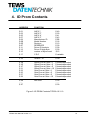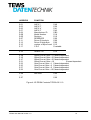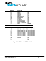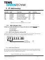
1
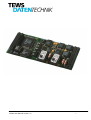
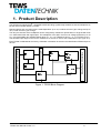
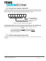
TIP500
Optically Isolated
16 Channel 12 Bit ADC
Version 1.0 Revision A
User Manual
Issue 1.2
14. April 1999
D75500801
TEWS DATENTECHNIK GmbH
Am Bahnhof 7
D-25469 Halstenbek
Germany
Tel +49 (0)4101 4058-0
Fax +49 (0)4101 4058-19
TIP500 User Manual Version 1.2
TIP500-10
optically isolated
16 channel 12 bit ADC
input voltage range ±10V
gain 1, 2, 5, 10
TIP500-11
optically isolated
16 channel 12 bit ADC
input voltage range ±10V
gain 1, 2, 4, 8
TIP500-20
optically isolated
16 channel 12 bit ADC
input voltage range 0V to +10V
gain 1, 2, 5, 10
TIP500-21
optically isolated
16 channel 12 bit ADC
input voltage range 0V to +10V
gain 1, 2, 4, 8
This manual covers all products
This document contains information, which is proprietary to TEWS DATENTECHNIK GmbH. Any reproduction
without written permission is forbidden.
TEWS DATENTECHNIK GmbH has made any effort to ensure that this manual is accurate and complete. However TEWS DATENTECHNIK GmbH reserves the right to change the product described in this document at any
time without notice.
Issue
Description
1.0
1.1
First issue
07. Feb. 1996
Technical Spec. 03. April 1996
TIP500 User Manual Version 1.2
Date
This product has been designed to operate with IndustryPackX compatible carriers. Connection to incompatible
hardware is likely to cause serious damage.
TEWS DATENTECHNIK GmbH is not liable for any damage arising out of the application or use of the device
described herin.
K1996 by TEWS DATENTECHNIK GmbH
IndustryPack is a registered trademark of GreenSpring Computers, Inc
TIP500 User Manual Version 1.2
1. Product Description . . . . . . . . . . . . . . . . . . . . . . . . . . . . . . . .
5
2. Technical Specification . . . . . . . . . . . . . . . . . . . . . . . . . . . .
6
3. Functional Description . . . . . . . . . . . . . . . . . . . . . . . . . . . . .
7
3.1. Analog Input . . . . . . . . . . . . . . . . . . . . . . . . . . . . . . . . . . . . . . . . . . . . .
3.2. Data Correction . . . . . . . . . . . . . . . . . . . . . . . . . . . . . . . . . . . . . . . . . . .
3.2.1. ADC Correction Formula . . . . . . . . . . . . . . . . . . . . . . . . . . . . . . . . . .
7
8
8
4. ID Prom Contents . . . . . . . . . . . . . . . . . . . . . . . . . . . . . . . . . .
9
5. IP Addressing . . . . . . . . . . . . . . . . . . . . . . . . . . . . . . . . . . . . . .
13
5.1. ADC Register Set . . . . . . . . . . . . . . . . . . . . . . . . . . . . . . . . . . . . . . .
5.1.1. ADC Control Register Address $00 . . . . . . . . . . . . . . . . . . . . . . . . .
5.1.1.1. ADC Channel Selection . . . . . . . . . . . . . . . . . . . . . . . . . . . . . . . . .
5.1.1.2. ADC Gain Selection . . . . . . . . . . . . . . . . . . . . . . . . . . . . . . . . . . . .
5.1.1.3. ADC Automatic Settling Time Control . . . . . . . . . . . . . . . . . . . . .
5.1.1.4. ADC Pipeline Mode Control . . . . . . . . . . . . . . . . . . . . . . . . . . . . . .
5.1.1.5. ADC Interrupt Enable . . . . . . . . . . . . . . . . . . . . . . . . . . . . . . . . . . .
5.1.2. ADC Data Register Address $02 . . . . . . . . . . . . . . . . . . . . . . . . . . .
5.1.3. ADC Status Register Address $05 . . . . . . . . . . . . . . . . . . . . . . . . .
5.1.4. ADC Convert Start Register Address $07 . . . . . . . . . . . . . . . . . . .
5.1.5. Interrupt Vector Register Address $09 . . . . . . . . . . . . . . . . . . . . . .
5.1.6. ID Write Enable Register Address $0B . . . . . . . . . . . . . . . . . . . . . .
13
13
13
14
14
15
15
15
17
17
18
18
6. Operating Modes
................................................
19
6.1. Mode Overview . . . . . . . . . . . . . . . . . . . . . . . . . . . . . . . . . . . . . . . . . . .
6.2. Automatic Mode . . . . . . . . . . . . . . . . . . . . . . . . . . . . . . . . . . . . . . . . . .
6.2.1. State Diagram Automatic Mode . . . . . . . . . . . . . . . . . . . . . . . . . . . .
6.2.2. Automatic Mode with Data Pipeline . . . . . . . . . . . . . . . . . . . . . . . . .
6.2.3. Automatic Mode without Data Pipeline . . . . . . . . . . . . . . . . . . . . . .
6.3. Normal Mode . . . . . . . . . . . . . . . . . . . . . . . . . . . . . . . . . . . . . . . . . . . .
6.3.1. State Diagram Normal Mode . . . . . . . . . . . . . . . . . . . . . . . . . . . . . .
6.3.2. Normal Mode with Data Pipeline . . . . . . . . . . . . . . . . . . . . . . . . . . .
6.3.3. Normal Mode without Data Pipeline . . . . . . . . . . . . . . . . . . . . . . . .
19
20
20
21
22
23
23
24
25
7. IP I/O connector . . . . . . . . . . . . . . . . . . . . . . . . . . . . . . . . . . . .
26
7.1. Analog Input Connections . . . . . . . . . . . . . . . . . . . . . . . . . . . . . . . . . .
7.2. Power Input Connections . . . . . . . . . . . . . . . . . . . . . . . . . . . . . . . . . .
26
27
TIP500 User Manual Version 1.2
Figure 1: TIP500 Block Diagram . . . . . . . . . . . . . . . . . . . . . . . . . . . . . . . . .
Figure 2: ID PROM Contents TIP500-10 V1.0 . . . . . . . . . . . . . . . . . . . . .
Figure 3: ID PROM Contents TIP500-11 V1.0 . . . . . . . . . . . . . . . . . . . . .
Figure 4: ID PROM Contents TIP500-20 V1.0 . . . . . . . . . . . . . . . . . . . . .
Figure 5: ID PROM Contents TIP500-21 V1.0 . . . . . . . . . . . . . . . . . . . . .
Figure 6: CONTREG Input Channel Selection and Mode . . . . . . . . . . . .
Figure 7: CONTREG Input Gain Selection . . . . . . . . . . . . . . . . . . . . . . . .
Figure 8: CONTREG Automatic Settling Time Control . . . . . . . . . . . . . .
Figure 9: CONTREG Pipeline Mode Control
..........................................................
Figure 10: CONTREG Interrupt Enable . . . . . . . . . . . . . . . . . . . . . . . . . . .
Figure 11: ADC Data Register . . . . . . . . . . . . . . . . . . . . . . . . . . . . . . . . . . .
Figure 12: Data Register Description . . . . . . . . . . . . . . . . . . . . . . . . . . . . .
Figure 13: ADC Status Register . . . . . . . . . . . . . . . . . . . . . . . . . . . . . . . . .
Figure 14: INTVEC Interrupt Vector Register . . . . . . . . . . . . . . . . . . . . . .
Figure 15: Operating Modes . . . . . . . . . . . . . . . . . . . . . . . . . . . . . . . . . . . .
Figure 16: State Diagram Automatic Mode . . . . . . . . . . . . . . . . . . . . . . . .
Figure 17: Flowchart Automatic Mode with Data Pipeline . . . . . . . . . . . .
Figure 18: Flowchart Automatic Mode without Data Pipeline . . . . . . . . .
Figure 19: State Diagram Normal Mode . . . . . . . . . . . . . . . . . . . . . . . . . .
Figure 20: Flowchart Normal Mode with Data Pipeline . . . . . . . . . . . . . .
Figure 21: Flowchart Normal Mode without Data Pipeline . . . . . . . . . . .
Figure 22: TIP500 Analog Input Connections . . . . . . . . . . . . . . . . . . . . . .
Figure 23: TIP500 Power Input Connections . . . . . . . . . . . . . . . . . . . . . .
TIP500 User Manual Version 1.2
1
5
6
7
8
9
10
10
11
11
11
11
13
14
15
16
17
18
19
20
21
22
23
1. Product Description
The TIP500 is an IndustryPack9 compatible module providing a galvanically isolated 16 channel multiplexed 12
bit ADC with on board DC/DC converter.
Data acquisition and conversion time is mode dependent: up to 10 ³s without channel / gain change and up to
12.5 ³s with channel / gain change.
The 16 input channels of the multiplexer can be configured by software to operate either in single ended mode
or in differential mode with eight inputs. The multiplexer of the ADC circuit is over voltage protected up to 70
Vp-p. A programmable gain amplifier allows gains of 1, 2, 5, 10 (TIP500-10/-20) or 1, 2, 4, 8 (TIP500-11/-21) .
The full scale input range is ±10V for the TIP500-10/-11 and 0V to 10V for the TIP500-20/-21 (for a gain of 1).
E
LW$'
FRWHQYHU
U
ZLK6
W+
3*$
JDLQ
RU
JDLQ
FKDQQHO
LQSXW
P
XOSWL
H[HU
,'
32
05
'&'&
FRWHQYHU
U
,QGXVWU\3DFN ,2 LQWHUIDFH
&RWUO RQ
,QWHIDFHU
RSWRFRXSOHUV
,QGXVWU\3DFN ORJLF LQWHUIDFH
Each TIP500 is calibrated at the factory. Calibration information is stored in the Identification PROM unique to
each IP.
Figure 1: TIP500 Block Diagram
TIP500 User Manual Version 1.2
2. Technical Specification
Logic Interface
IndustryPack9 Logic Interface
Size
single wide IP
I/O Interface
50-conductor flat cable
Analog Inputs
16 single ended channels or
8 differential channels
Input Isolation
All channels are galvanically isolated from the IP Interface.
DC/DC converter on board.
Input Gain Amplifier
Programmable for gain 1, 2, 5, 10 (TIP500-10 and TIP500-20)
Programmable for gain 1, 2, 4, 8 (TIP500-11 and TIP500-21)
Input Voltage Range
TIP500-10:
±10V,
±5V ,
±2V ,
±1V ,
TIP500-20:
0V to 10V
0V to 5V
0V to 2V
0V to 1V
(gain = 1)
(gain = 2)
(gain = 5)
(gain = 10)
TIP500-11:
±10V,
±5V,
±2.5V,
±1.25V,
TIP500-21:
0V to 10V
0V to 5V
0V to 2.5V
0V to 1.25V
(gain = 1)
(gain = 2)
(gain = 4)
(gain = 8)
Input Over Voltage
Input over voltage protection up to 70V p-p
Input ADC
12 bit ADC; data acquisition and conversion time up to 10³s
without channel / gain change and up to 12.5³s with channel /
gain change (mode dependent).
Calibration Data
Calibration data for gain and offset correction in ID PROM
Accuracy
± 1LSB, after calibration for all TIP500 Modules.
Linearity
± 1LSB for all TIP500 Modules
Wait States
IDSEL 1 wait state
IOSEL 0 wait state
INTSEL 0 wait state
Power Requirements
typ. 310 mA @ 5V
Temperature Range
Operating -40EC to 85EC
Storage -45EC to 125EC
Humidity
5 - 95% non-condensing
TIP500 User Manual Version 1.2
3. Functional Description
3.1. Analog Input
The TIP500 provides 16 single ended or 8 differential multiplexed analog inputs for. The desired input and the
mode (single ended or differential) is selected by programming the input multiplexer.
A software programmable gain amplifier with gain settings of 1, 2, 5 and 10 for the TIP500-10, -20 and 1, 2, 4
and 8 for the TIP500-11, -21 allows a direct connection of a wide range of sensors and instrumentation. The maximum analog input voltage range is ±10V at a gain of 1 for the TIP500-10 and TIP500-11. For the TIP500-20 and
-21 the maximum analog input voltage range is 0V to 10V at a gain of 1.
The ADC is a 12 bit ADS7808 with a maximum sample and conversion time of 10³s . The 12 bit data are alined
in the bits 15-4 of a 16 bit data word, bits 3-0 are always zero.
In multiplexed analog input systems a settling time must expire before the data can be converted after the change
of the input channel. This settling time is depended on the programmed gain. At the most analog input solutions
it is the responsibility of the user to observe the settling time. The TIP500 module has an Automatic Settling Time
Control mode. If this mode is enabled, a write to the ADC Control Register, which is necessary to select a new
input channel by the multiplexer, initiates a data conversion automatically after the settling time has expired.
The absolute accuracy of the module is increased by using the possibility to correct the data by software with
factory calibration factors, which are stored in the individual ID PROM of the module.
TIP500 User Manual Version 1.2
3.2. Data Correction
There are two errors which affect the DC accuracy of the ADC. The first is the zero error (offset). This is the data
value when converting with the input connected with its own ground in single ended mode, or with shorted inputs
in differential mode. This error is corrected by subtracting the known error from all readings.
The second error is the gain error. Gain error is the difference between the ideal gain and the actual gain of the
programmable gain amplifier and the ADC. It is corrected by multiplying the data value by a correction factor.
The data correction values are obtained during factory calibration and are stored in the modules individual version of the ID PROM. The ADC has a pair of offset and gain correction values for each of the programmable gains.
The correction values are stored in the ID PROM as two’s complement byte wide values in the range -128 to
127. For higher accuracy they are scaled to ¼ LSB.
3.2.1. ADC Correction Formula
The basic formula for correcting any ADC reading for the TIP500-10 / -11 ( input voltage range +/- 10V ) is :
Value = Reading * ( 1 - GainFRUU / 8192 ) - Offset
FRUU *
4
The basic formula for correcting any ADC reading for the TIP500-20 / -21 ( input voltage range 0V to 10V ) is:
Value = Reading * ( 1 - Gain FRUU / 16384 ) - Offset FRUU * 4
Value is the corrected result, Reading is the data read from the ADC, Gaincorr and Offsetcorr are the correction
factors from the ID PROM.
Gaincorr and Offsetcorr correction factors are stored for each for the possible gain settings.
1RWH
)ORDWLQJ SRLQW DULWKPHWLFV RU VFDOHG LQWHJHU DULWKPHWLFV LV QHFHVVDU\ WR
DYRLG URXQGLQJ HUURU ZKLOH FRPSXWLQJ DERYH IRUPXOD
TIP500 User Manual Version 1.2
4. ID Prom Contents
ADDRESS
FUNCTION
$ 01
$ 03
$ 05
$ 07
$ 09
$ 0B
$ 0D
$ 0F
$ 11
$ 13
$ 15
$ 17
ASCII ’I’
ASCII ’P’
ASCII ’A’
ASCII ’C’
Manufacturer ID
Model Number
Revision
RESERVED
Driver-ID low-byte
Driver-ID high-byte
number of bytes used
CRC
$ 49
$ 50
$ 41
$ 43
$ B3
$ 18
$ 10
$ 00
$ 00
$ 00
$ 15
$ variable
$ 19
Version -10
$ 0A
$ 1B
$ 1D
$ 1F
$ 21
$ 23
$ 25
$ 27
$ 29
Offset Error at Gain = 1
Offset Error at Gain = 2
Offset Error at Gain = 5
Offset Error at Gain = 10
Gain Error at Gain = 1
Gain Error at Gain = 2
Gain Error at Gain = 5
Gain Error at Gain = 10
$ board dependent
$ board dependent
$ board dependent
$ board dependent
$ board dependent
$ board dependent
$ board dependent
$ board dependent
$ 2B
......
$ 3F
Not used
$ 00
.......
$ 00
Figure 2: ID PROM Contents TIP500-10 V1.0
TIP500 User Manual Version 1.2
ADDRESS
FUNCTION
$ 01
$ 03
$ 05
$ 07
$ 09
$ 0B
$ 0D
$ 0F
$ 11
$ 13
$ 15
$ 17
ASCII ’I’
ASCII ’P’
ASCII ’A’
ASCII ’C’
Manufacturer ID
Model Number
Revision
RESERVED
Driver-ID low-byte
Driver-ID high-byte
number of bytes used
CRC
$ 49
$ 50
$ 41
$ 43
$ B3
$ 18
$ 10
$ 00
$ 00
$ 00
$ 15
$ variable
$ 19
Version -11
$ 0B
$ 1B
$ 1D
$ 1F
$ 21
$ 23
$ 25
$ 27
$ 29
Offset Error at Gain = 1 $ board dependent
Offset Error at Gain = 2 $ board dependent
Offset Error at Gain = 4 $ board dependent
Offset Error at Gain = 8 $ board dependent
Gain Error at Gain = 1 $ board dependent
Gain Error at Gain = 2 $ board dependent
Gain Error at Gain = 4 $ board dependent
Gain Error at Gain = 8 $ board dependent
$ 2B
......
$ 3F
Not used
$ 00
.......
$ 00
Figure 3: ID PROM Contents TIP500-11 V1.0
TIP500 User Manual Version 1.2
ADDRESS
FUNCTION
$ 01
$ 03
$ 05
$ 07
$ 09
$ 0B
$ 0D
$ 0F
$ 11
$ 13
$ 15
$ 17
ASCII ’I’
ASCII ’P’
ASCII ’A’
ASCII ’C’
Manufacturer ID
Model Number
Revision
RESERVED
Driver-ID low-byte
Driver-ID high-byte
number of bytes used
CRC
$ 49
$ 50
$ 41
$ 43
$ B3
$ 18
$ 10
$ 00
$ 00
$ 00
$ 15
$ variable
$ 19
Version -20
$ 14
$ 1B
$ 1D
$ 1F
$ 21
$ 23
$ 25
$ 27
$ 29
Offset Error at Gain = 1 $ board dependent
Offset Error at Gain = 2 $ board dependent
Offset Error at Gain = 5 $ board dependent
Offset Error at Gain = 10
$ board dependent
Gain Error at Gain = 1 $ board dependent
Gain Error at Gain = 2 $ board dependent
Gain Error at Gain = 5 $ board dependent
Gain Error at Gain = 10 $ board dependent
$ 2B
......
$ 3F
Not used
$ 00
.......
$ 00
Figure 4: ID PROM Contents TIP500-20 V1.0
TIP500 User Manual Version 1.2
ADDRESS
FUNCTION
$ 01
$ 03
$ 05
$ 07
$ 09
$ 0B
$ 0D
$ 0F
$ 11
$ 13
$ 15
$ 17
ASCII ’I’
ASCII ’P’
ASCII ’A’
ASCII ’C’
Manufacturer ID
Model Number
Revision
RESERVED
Driver-ID low-byte
Driver-ID high-byte
number of bytes used
CRC
$ 49
$ 50
$ 41
$ 43
$ B3
$ 18
$ 10
$ 00
$ 00
$ 00
$ 15
$ variable
$ 19
Version -21
$ 15
$ 1B
$ 1D
$ 1F
$ 21
$ 23
$ 25
$ 27
$ 29
Offset Error at Gain = 1 $ board dependent
Offset Error at Gain = 2 $ board dependent
Offset Error at Gain = 4 $ board dependent
Offset Error at Gain = 8 $ board dependent
Gain Error at Gain = 1 $ board dependent
Gain Error at Gain = 2 $ board dependent
Gain Error at Gain = 4 $ board dependent
Gain Error at Gain = 8 $ board dependent
$ 2B
......
$ 3F
Not used
$ 00
.......
$ 00
Figure 5: ID PROM Contents TIP500-21 V1.0
TIP500 User Manual Version 1.2
5. IP Addressing
The TIP500 is controlled by a set of registers, which are directly accessible in the IO address space of the IP.
ADDRESS
NAME
FUNCTION
SIZE
ACCESS
$ 00
$ 02
$ 05
$ 07
$ 09
$ 0B
CONTREG
DATAREG
STATREG
CONVERT
INTVEC
IDWRENA
ADC Control Register
ADC Data Register
ADC Status Register
ADC Convert Start Register
Interrupt Vector Register
ID-PROM write enable
word
word
byte
byte
byte
byte
R/W
R/W
RO
WO
R/W
WO
1RWH
,':5(1$ LV IRU IDFWRU\ XVH RQO\ GR QRW ZULWH WR WKLV UHJLVWHU
5.1. ADC Register Set
The ADC of the TIP500 is controlled by a set of 4 registers. All registers are cleared by IP_RESET.
ADC Control Register
ADC Data Register
ADC Status Register
ADC Convert Start Register
5.1.1. ADC Control Register Address $00
The ADC Control Register CONTREG is used to select an input channel, the gain and the mode for the next
data conversion. This is done by writing the corresponding bit pattern into bit 0 to bit 9.
; ; ; ; ; ;
unused bits
access undefined
access don’t care
read
write
5.1.1.1. ADC Channel Selection
Bit 0 to bit 3 of the ADC Control Register CONTREG are used to select an input channel for the data conversion.
Bit 4 of the ADC Control Register CONTREG is used to control if the module operates in differential or in single
ended mode. If this bit is set to ’1’ differential mode is selected.
Figure 6: CONTREG Input Channel Selection and Mode
TIP500 User Manual Version 1.2
'
)
,
&6
&6
&6
&6
,QSXW &KDQQHO 6HOHFWLRQ
'LIIHUHQWLDO 6LQJOH (QGHG
&+
&+
&+
&+
'LIIHUHQWLDO 0RGH
1RWH
,Q GLIIHUHQWLDO PRGH RQO\ FKDQQHOV WR PD\ EH VHOHFWHG ,Q WKLV PRGH
FKDQQHOV WR DUH XVHG DV LQSXW IRU FKDQQHOV WR 5.1.1.2. ADC Gain Selection
Bit 5 and bit 6 of the ADC Control Register CONTREG are used to program the gain of the input amplifier.
*$
1
, *$
1
, *DLQ 6HOHFWLRQ
7,3 7,3 *
*
*
* *
*
*
*
Figure 7: CONTREG Input Gain Selection
5.1.1.3. ADC Automatic Settling Time Control
If bit 7 of the ADC Control Register CONTREG is set to ’1’, the Automatic Mode for the settling time is enabled.
In this mode a data conversion is initiated by writing to the ADC Control Register CONTREG, but however is
automatically delayed by hardware until the gain depended settling time has expired.
If bit 7 of the ADC Control Register CONTREG is set to ’0’, the Normal Mode for the settling time is enabled.
In this mode a data conversion is initiated by writing to the ADC Convert Start Register CONVERT after selecting
the desired channel and gain by writing to the ADC Control Register CONTREG.
$6
7
&(
$XWRPDWLF 6HWWOLQJ 7LPH &RQWURO (QDEOH
Figure 8: CONTREG Automatic Settling Time Control
TIP500 User Manual Version 1.2
1RWH
7KH VHWWOLQJ WLPH IRU DOO 7,3 0RGXOHV LV ³V IRU DOO JDLQV
5.1.1.4. ADC Pipeline Mode Control
If bit 8 is set to ’1’ the pipeline mode is selected. In pipeline mode the result from the conversion (N-1) is shifted
into the ADC Data Register DATAREG during the conversion N.
3
,/
3LSOLQH 0RGH VHOHFW
Figure 9: CONTREG Pipeline Mode Control
5.1.1.5. ADC Interrupt Enable
Bit 8 of the ADC Control Register CONTREG is used to enable interrupt generation of the module. If this bit is
set to ’1’ interrupts are always initiated, whenever the settling time is over ( on IP_INTREQ1 ) and data conversion has been completed ( on IP_INTREQ0 ). If the module is in the automatic mode ( bit7 set to ’1’ ) only one
interrupt at the end of data conversion ( on IP_INTREQ0 ) is being generated.
1
,7
(1$
,QWHUUXSW (QDEOH
Figure 10: CONTREG Interrupt Enable
5.1.2. ADC Data Register Address $02
The ADC Data Register DATAREG contains the converted data value. The 12 bit ADC value is shifted in the
higher bit’s of the data register by hardware . This allows direct processing of the data as a 16 bit two’s complement integer value for the TIP500-10/11 and 16 bit straight binary for TIP500-20/21.
ELW $'& GDWD
Figure 11: ADC Data Register
Figure 12: Data Register Description
TIP500 User Manual Version 1.2
',*,7$/ 287387
'(6&5,37,21
ELQDU\ WZR
V
FRPSOHPHQW
7,3 )XOO 6FDOH )6 /6%
0LGVFDOH
2QH /6% %HORZ 0LGVFDOH
)XOO 6FDOH
))
)))
VWUDLJKW ELQDU\
7,3 )))
))
1RWH
7KH FRQWHQWV RI $'& 'DWD 5HJLVWHU '$7$5(* LV QRW YDOLG DV ORQJ DV WKH
$'& %XV\ )ODJ LV UHDG DV TIP500 User Manual Version 1.2
5.1.3. ADC Status Register Address $05
Bit 0 and bit 1 of the ADC Status Register STATREG reflect the status of the ADC converter. As long as bit 0
is read as ’1’, the settling time did not expire after writing to the ADC Control Register CONTREG. Bit 1 indicates
the busy status of the ADC converter itself ( ’1’ = ADC busy ). If Automatic Mode is active bit 1 indicates a ’1’
during the settling time and the conversion time.
$
'
&
%
XV\
6
HWOW
%
XV\
6HWWOLQJ 7LPH %XV\
$'& %XV\
Figure 13: ADC Status Register
1RWH
%LW RI WKH $'& 6WDWXV 5HJLVWHU DUH XQGHILQHG
5.1.4. ADC Convert Start Register Address $07
If the TIP500 is configured in Normal Mode writing any value into the ADC Convert Register CONVERT starts
a data conversion immediately.
1RWH
,Q QRUPDO PRGH LW LV LQ WKH UHVSRQVLELOLW\ RI WKH XVHU WR REVHUYH WKH VHW
WOLQJ WLPH EXV\ IODJ DQG WKH $'& EXV\ IODJ RI WKH $'& 6WDWXV 5HJLVWHU
:ULWHV WR WKH $'& &RQYHUW 6WDUW 5HJLVWHU &219(57 GXULQJ $'& EXV\
DUH LJQRUHG
TIP500 User Manual Version 1.2
5.1.5. Interrupt Vector Register Address $09
The Interrupt Vector Register INTVEC is a byte wide read/write register. The Interrupt Vector Register is shared
between both interrupt sources, but both, the settling time ready and the ADC data ready will create an individual
interrupt. A read cycle to the INTVEC Register acknowledges and clears the interrupt.
;
:LOO UHDG DW LQWHUUXSW DV
IRU $'& GDWD UHDG\
IRU VHWWOLQJ WLPH UHDG\
,QWHUUXSW YHFWRU ORDGHG
E\ VRIWZDUH
Figure 14: INTVEC Interrupt Vector Register
For an interrupt from settling time ready bit 0 of the interrupt vector will read as ’1’. For an interrupt from the
ADC data ready bit 0 will read as ’0’. If the vector register is for example loaded with ’$60’, settling time ready
will create an interrupt at vector ’$61’ and ADC data ready will create an interrupt at vector ’$60’.
1RWH
7KH LQWHUUXSW VHWWOLQJ WLPH UHDG\ LV FUHDWHG E\ WKH IDOOLQJ HGJH RI VHWWOLQJ
WLPH EXV\ VWDWXV DQG XVHV WKH ,175(4 WKH LQWHUUXSW $'& UHDG\ LV
FUHDWHG E\ WKH IDOOLQJ HGJH RI $'& EXV\ VWDWXV DQG XVHV WKH ,175(4
LQWHUUXSW OLQH RI WKH ,3 EXV
5.1.6. ID Write Enable Register Address $0B
This register is for factory use only. Do not write to this register. If bit 0 is set ’1’ a write access to the ID-PROM
is enabled.
TIP500 User Manual Version 1.2
6. Operating Modes
The TIP500 supports four operating modes which are selected with bit 7 ( Normal / Automatic Mode ) and bit
8 ( Pipeline / no Pipeline Mode ) of the ADC Control Register CONTREG.
6.1. Mode Overview
- 1RUPDO 0RGH 1R 3LSHOLQH 0RGH
- $XWRPDWLF 0RGH 1R 3LSHOLQH 0RGH
- 1RUPDO 0RGH 3LSHOLQH 0RGH
- $XWRPDWLF 0RGH 3LSHOLQH 0RGH
CONTREG Bit 7 = 1
CONTREG Bit 7 = 0
Automatic Mode
Normal Mode
After the settling time
has expired conversion
CONTREG Bit 8 = 1 N is started and the
result of conversion
Pipline Mode
N-1 is shifted into the
ADC Data Register.
A write access to the
CONVERT register
starts conversion N and
shifts the result of
conversion N-1 into the
ADC Data Register.
After the settling time
has expired conversion
CONTREG Bit 8 = 0 N is started and the
result of conversion N
is shifted into the ADC
No Pipline Mode
Data Register.
A write access to the
CONVERT register
starts conversion N and
shifts the result of
conversion N into the
ADC Data Register.
Figure 15: Operating Modes
1RWH
,Q 1RUPDO 0RGH WKH XVHU VKRXOG REVHUYH WKH VHWWOLQJ WLPH E\ WKH VHWWOH
EXV\ IODJ LQ WKH $'& 6WDWXV 5HJLVWHU
TIP500 User Manual Version 1.2
6.2. Automatic Mode
The Automatic Mode is enabled by setting bit 7 of the ADC Control Register CONTREG to ’1’. A write access
to the ADC Control Register CONTREG with bit 7 set to ’1’ start a conversion for the programmed channel and
gain after the settling time has expired. In Pipeline Mode ( bit 8 of the ADC Control Register CONTREG set to
’1’ ) the result of the previous conversion is shifted into the ADC Data Register DATAREG during the actual conversion. If the Pipeline Mode is switched off the result of the actual conversion is shifted into the ADC Data Register DATAREG.
6.2.1. State Diagram Automatic Mode
QR F\FOH QH[W
$'& EXV\
$'& EXV\
5(6(7
,'/(
ZULWH DFFHVV WR &2175(*
%86<
Figure 16: State Diagram Automatic Mode
In Automatic Mode the ADC busy flag is active during the whole cycle of channel/gain select, settling time and
data conversion. When the ADC busy flag becomes inactive ( = ’0’ ) the conversion result is accessible in the
ADC Data Register DATAREG and an interrupt will be generated if interrupts are enabled.
TIP500 User Manual Version 1.2
6.2.2. Automatic Mode with Data Pipeline
If Automatic Mode with Pipeline is selected during conversion N the result of conversion N-1 is shifted into the
ADC Data Register DATAREG. The acquisition and conversion time in this mode is 20³s.
67$57
Write access to the ADC Control Register
starts automatically the conversion N after
the settling time has expired and shifts the
result of conversion N-1 into the ADC Data
Register.
select new
gain & channel
Auto & Pipeline active
Bit1 of the ADC Status Register indicates
ADC busy during the whole cycle.
ADC
BUSY
"
\
Q
read data of
conversion N-1
Read data of the conversion N-1 from ADC
Data Register
Figure 17: Flowchart Automatic Mode with Data Pipeline
TIP500 User Manual Version 1.2
6.2.3. Automatic Mode without Data Pipeline
If Automatic Mode without Pipeline is selected the result of the actual conversion is shifted into the ADC Data
Register DATAREG. The acquisition and conversion time in this mode is 30³s.
67$57
Write access to the ADC Control Register
starts automatically the conversion after the
settling time has expired and shifts the result
into the ADC Data Register.
select new
gain & channel
Auto active
Bit1 of the ADC Status Register indicates ADC
busy during the whole cycle.
ADC
BUSY
"
\
Q
read data of
conversion (n)
Read data of the actual conversion from the
ADC Data Register
Figure 18: Flowchart Automatic Mode without Data Pipeline
TIP500 User Manual Version 1.2
6.3. Normal Mode
The Normal Mode is enabled by setting bit 7 of the ADC Control Register CONTREG to ‘0‘. A write access to
the ADC Control Register CONTREG with bit 7 set to ’0’ ( Normal Mode enabled ) selects a new channel and
gain for the next conversion. As long as the settling time expires bit 0 of the ADC Status Register STATREG (
settle busy flag ) reads as ‘1‘. After the settling time has expired a conversion can be started by writing to the
ADC Convert Start Register CONVERT. To achieve higher conversion rates it is possible to select a new channel
and gain for the next conversion after the previous conversion has been started. In this mode the settling time
for the new channel and the conversion time of the actual channel proceed simultaneously. As long as bit 1 of
the ADC Status Register STATREG ( ADC busy flag ) reads as ‘1‘ conversion is in progress. Reading bit 1 of
the ADC Status Register as ‘0‘indicates that the conversion result is accessible in the ADC Data Register DATAREG.
If interrupts are enabled two interrupts will be generated: the first interrupt at the end of the settling time, the
second interrupt at the end of conversion.
6.3.1. State Diagram Normal Mode
$'& EXV\
6HWWOH EXV\
6(77/(B
%86<
$'&
%86<
$
&
%
'
5(6(7
,'/(
$ :ULWH DFFHVV WR &2175(*
% 6HWWOLQJ WLPH H[SLUHG
& :ULWH DFFHVV WR &219(57
' $'& UHDG\ FRQYHUVLRQ UHVXOW LQ
$'& 'DWD 5HJLVWHU
QR F\FOH QH[W
Figure 19: State Diagram Normal Mode
TIP500 User Manual Version 1.2
6.3.2. Normal Mode with Data Pipeline
If Normal Mode with Pipeline is selected during conversion N the result of conversion N-1 is shifted into the ADC
Data Register DATAREG. In this mode it is possible that the settling time and conversion time simultaneous proceed. The acquisition and conversion time in this mode is 10³s with no change of channel / gain and 12.5³s with
change of channel / gain.
67$57
:ULWH DFFHVV WR $'& &RQWURO 5HJLVWHU
select gain & channel
Pipeline active
Read bit 0 of ADC Status Register to check for
end of settling time.
SETTLE
BUSY
"
\
Q
Write access to ADC Start Convert Register
starts conversion N and shifts result of
conversion N-1 into the ADC Data Register.
VWDUW FRQYHUVLRQ
Select a new channel and a new gain
during conversion proceeds by a write
access to the ADC Control Register.
select new gain & new
channel
Pipeline active
ADC BUSY
"
\
Read bit1 of the ADC Status Register
to check for end of conversion.
Q
read data of
conversion N-1
Read result of the conversion N-1
from ADC Data Register.
Figure 20: Flowchart Normal Mode with Data Pipeline
1RWH
)RU FRQYHUVLRQV ZLWKRXW FKDQQHO DQG JDLQ FKDQJH LW LV QRW QHFHVVDU\ WR
REVHUYH WKH VHWWOH EXV\ IODJ RI WKH $'& 6WDWXV 5HJLVWHU
TIP500 User Manual Version 1.2
6.3.3. Normal Mode without Data Pipeline
If Normal Mode without Pipeline is selected the result of the actual conversion is shifted into the ADC Data Register DATAREG. In this mode it is possible that the settling time and conversion time simultaneous proceed. The
acquisition and conversion time in this mode is 20³s.
67$57
:ULWH DFFHVV WR $'& &RQWURO 5HJLVWHU
select gain & channel
Read bit 0 of ADC Status Register to check for
end of settling time.
SETTLE BUSY
"
\
Q
Write access to ADC Start Convert Register
starts conversion and shifts result of conversion
into the ADC Data Register.
VWDUW FRQYHUVLRQ
Select a new channel and a new gain
during conversion proceeds by a write
access to the ADC Control Register.
select new gain & channel
ADC
BUSY"
\
Read bit1 of the ADC Status Register
to check for end of conversion.
Q
read data of
conversion
Read result of the conversion from
ADC Data Register.
Figure 21: Flowchart Normal Mode without Data Pipeline
1RWH
)RU FRQYHUVLRQV ZLWKRXW FKDQQHO DQG JDLQ FKDQJH LW LV QRW QHFHVVDU\ WR
REVHUYH WKH VHWWOH EXV\ IODJ RI WKH $'& 6WDWXV 5HJLVWHU
TIP500 User Manual Version 1.2
7. IP I/O connector
7.1. Analog Input Connections
Pin-Number
Mode
Single Ended
Differential
01
02
03
04
05
06
07
08
09
10
11
12
13
14
15
16
17
18
19
20
21
22
23
24
ADC Input 1
ADC Input 9
AGND
ADC Input 10
ADC Input 2
AGND
ADC Input 3
ADC Input 11
AGND
ADC Input 12
ADC Input 4
AGND
ADC Input 5
ADC Input 13
AGND
ADC Input 14
ADC Input 6
AGND
ADC Input 7
ADC Input 15
AGND
ADC Input 16
ADC Input 8
AGND
ADC Input 1 +
ADC Input 1 AGND
ADC Input 2 ADC Input 2 +
AGND
ADC Input 3 +
ADC Input 3 AGND
ADC Input 4 ADC Input 4 +
AGND
ADC Input 5 +
ADC Input 5 AGND
ADC Input 6 ADC Input 6 +
AGND
ADC Input 7 +
ADC Input 7 AGND
ADC Input 8 ADC Input 8 +
AGND
Figure 22: TIP500 Analog Input Connections
TIP500 User Manual Version 1.2
7.2. Power Input Connections
Pin-Number
Function
44
45
46
47
48
49
50
AGND
-15V
AGND
+15V
AGND
+5V
AGND
Figure 23: TIP500 Power Input Connections
1RWH
7KH SRZHU LQSXW FRQQHFWLRQV DUH UHVHUYHG IRU VSHFLDO YHUVLRQV RI WKH
7,3 ZLWKRXW RQ ERDUG '&'& FRQYHUWHU
TIP500 User Manual Version 1.2