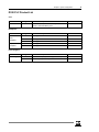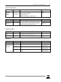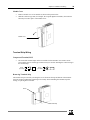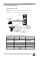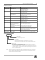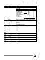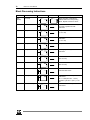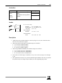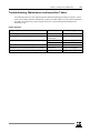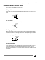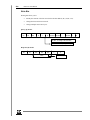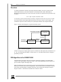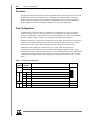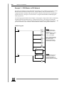
1
D320 PLC User’s Manual The information contained in this manual is the property of Cutler-Hammer, Inc. Information in this manual is subject to change without notice and does not represent a commitment on the part of CutlerHammer, Inc. Any Cutler-Hammer software described in this manual is furnished under a license agreement. The software may be used or copied only in accordance with the terms of the agreement. It is against the law to copy the software on any medium except as specifically allowed in the agreement. No part of this manual may be reproduced or transmitted in any form or by any means, electronic, mechanical, photocopying, recording or otherwise, without prior written permission of Cutler-Hammer, Inc. RESTRICTED RIGHTS LEGEND Use, duplication, or disclosure by the Government is subject to restrictions set forth in paragraph (b)(3)(B) of the Rights in Technical Data and Computer Software clause of DAR 7-104.9(a). Contractor/Manufacturer is Cutler-Hammer, P.O. Box 6166, Westerville, OH 43086-6166. TRADEMARKS Commercial names of products from other manufacturers or developers that appear in this manual are registered or unregistered trademarks of those respective manufacturers or developers, which have expressed neither approval nor disapproval of Cutler-Hammer products. Copyright Cutler-Hammer, Inc. 1998. All rights reserved. Catalog Number D320SA100 P/N 01-00408-02 Preface Preface Welcome to Cutler-Hammer’s D320 PLC User's Manual. This preface describes the contents of this manual and provides information on Support Services. i ii D320 PLC User's Manual About This Manual Purpose This manual focuses on describing the D320 Programmable Logic Controller (PLC). What’s Inside This manual is organized in the following way: Preface Chapter 1: Introduction Chapter 2: System Configuration Chapter 3: Product Specification Chapter 4: Installation and Wiring Chapter 5: CPU Operation and Memory Chapter 6: Instructions Chapter 7: Testing and Troubleshooting Chapter 8: Troubleshooting Noise Problems Chapter 9: External Dimensions Appendix A: D320 PLC Communication Protocol Appendix B: PID Loop Control Appendix C: COM2 UDCP Specification Preface iii Support Services It is Cutler-Hammer’s goal to ensure your greatest possible satisfaction with the operation of our products. We are dedicated to providing fast, friendly, and accurate assistance. That is why we offer you so many ways to get the support you need. Whether it’s by phone, fax, modem, or mail, you can access Cutler-Hammer support information 24 hours a day, seven days a week. Our wide range of services include: Technical Support 1-800-809-2772 If you are in the U.S. or Canada, you can take advantage of our toll-free line for technical assistance with hardware and software product selection, system design and installation, and system debugging and diagnostics. Technical support engineers are available for calls during regular business hours (8 am - 5:30 pm EST) by calling 1-800-809-2772. International calls can be made to either the Tech Line at 1-800-809-2772 (toll call) or the Cutler-Hammer main business line at 614-882-3282. Emergency Technical Support 1-800-809-2772 Because machines do not run on a nine-to-five schedule, we offer emergency after-hours technical support. A technical support engineer can be paged for emergencies involving plant down situations or safety issues. Emergency support calls are automatically routed directly to our answering service afterhours (5:30 pm - 8 am EST) and weekends. For emergency technical support, call 1-800-809-2772. Does not currently include product repairs or shipping outside normal business hours. Technical Support Fax 614-882-0417 You can also contact our technical support engineers by faxing your support requests directly to APSC Westerville at 614-882-0417. Information Fax-Back Service 614-899-5323 The latest Cutler-Hammer product information, specifications, technical notes and company news is available to you via fax through our direct document request service at 614-899-5323. Using a touchtone phone, you can select any of the info faxes from our automated product literature and technical document library, punch in a fax number and receive the information immediately. Bulletin Board Service 614-899-5209 Parameters: 8 data bits, 1 stop bit, parity none, 9600-28.8K baud. If you have modem access, you can dial in directly to our electronic bulletin board service for the latest product and company information. File sharing, product software downloads and our user message service are just a few of the things you will find online at 614-899-5209. Website and E-mail Address http://www.cutlerhammer.eaton.com/automation [email protected] If you have Internet capabilities, you also have access to technical support via our website at http://www.cutlerhammer.eaton.com. The website includes technical notes, frequently asked questions, release notes, and other technical documentation. This direct technical support connection also offers you the ability to request assistance and exchange software files electronically. Technical support messages and files can be sent to [email protected]. iv D320 PLC User's Manual Software Update Service 1-800-809-2772 FAX 614-899-4141 We also offer you the opportunity to take advantage of software upgrades, advanced software notices, and special software promotions through our Software Update Service. When you register your software, you will receive one-year of free or reduced-price upgrades along with all the other benefits of membership, including 48-hour shipping of software upgrades. Contact the Software Update Service at 1-800-809-2772 or fax 614-899-4141. Repair and Upgrade Service 614-882-3282 ext. 7601 FAX 614-882-3414 Our well-equipped Customer Service department is ready to assist you with repairs, upgrades, and spare parts services. If a situation arises where one of these services is needed, just call 614-882-3282 x7601 or fax 614-882-3414. Product Ordering Service 614-882-3282 FAX 614-882-6532 Authorized Cutler-Hammer distributors may place product orders directly with our Order Processing department by calling 614-882-3282 x406 or faxing 614-882-6532. For information on your local distributor, call the Cutler-Hammer Tech Line. Customer Support Center 1-800-356-1243 Authorized Cutler-Hammer distributors and Cutler-Hammer sales offices can get assistance for CutlerHammer standard and component product lines through the Customer Support Center. Call the Customer Support Center for the following assistance: 1. Stock availability, proof of shipment, or to place an order. 2. Expedite an existing order. 3. Product assistance and product price information. 4. Product returns other than warranty returns. For information on your local distributor or sales office, call the Cutler-Hammer Tech Line at 1-800809-2772. Correspondence Address Cutler-Hammer 173 Heatherdown Drive Westerville, OH 43081 Table of Contents v Table of Contents Preface I About This Manual ................................................................................................................................................ii Purpose...........................................................................................................................................................ii What's Inside ..................................................................................................................................................ii Support Services....................................................................................................................................................iii Table of Contents v Chapter 1: Introduction 1 Overview of the Manual......................................................................................................................................... 2 Features of the D320 PLC...................................................................................................................................... 2 Self Diagnostics ............................................................................................................................................. 3 PID Loop Control........................................................................................................................................... 3 Real-time Clock ............................................................................................................................................. 3 Large Program Memory................................................................................................................................. 3 NOVRAM Battery Backup ............................................................................................................................ 3 I/O and Special Function Module Support..................................................................................................... 3 Peripheral Support.......................................................................................................................................... 4 System Installation Considerations ........................................................................................................................ 4 Environmental Considerations ....................................................................................................................... 4 Installing Modules on the System .................................................................................................................. 4 Removing Modules from the System............................................................................................................. 4 Preventing PLC System Malfunctions ........................................................................................................... 5 Chapter 2: System Configuration 7 D320 PLC System Components............................................................................................................................. 8 D320 PLC Product List .......................................................................................................................................... 9 D320 PLC I/O Configuration............................................................................................................................... 14 Module Placement Requirements................................................................................................................. 14 D320 PLC Backplane Configurations.................................................................................................................. 15 Chapter 3: Product Specification 17 Environmental Operating Ranges ........................................................................................................................ 18 CPU Performance Specifications ......................................................................................................................... 19 Name and Function of CPU Components .................................................................................................... 20 Chapter 4: Installation And Wiring 23 System Design Considerations............................................................................................................................. 24 Power Supply Wiring................................................................................................................................... 24 Interlock Circuit and Emergency Stop Circuit (Safety measures in system design) .................................... 24 Momentary Power Failure and Voltage Drop .............................................................................................. 25 System Installation Guidelines............................................................................................................................. 25 Environmental Usage Conditions................................................................................................................. 25 Control Panel Installation............................................................................................................................. 26 System Wiring and Installation Procedures ......................................................................................................... 28 Installation Dimensions................................................................................................................................ 28 Module Installation ...................................................................................................................................... 29 Unit Installation Height................................................................................................................................ 30 vi D320 PLC User's Manual Expansion Cable Connection....................................................................................................................... 30 Power Supply Wiring .......................................................................................................................................... 31 Power wiring................................................................................................................................................ 31 Grounding.................................................................................................................................................... 31 120/240 VAC Power Supply Wiring Diagram ............................................................................................ 32 I/O Module Wiring .............................................................................................................................................. 33 Digital Input Module Wiring ....................................................................................................................... 33 Digital Output Module Wiring .................................................................................................................... 37 Installation Precautions for I/O Modules ..................................................................................................... 38 Terminal Strip Wiring.................................................................................................................................. 39 Connector Module Wiring ........................................................................................................................... 40 Connector Module Wiring ........................................................................................................................... 40 Alarm Output of Power Supply ................................................................................................................... 42 PLC Communications Wiring ............................................................................................................................. 43 Connecting the PLC to a PC ........................................................................................................................ 43 D320 CPU Module Communication Specification...................................................................................... 43 Chapter 5: CPU Operation And Memory 45 Terminology ........................................................................................................................................................ 46 Overview of CPU Operation Mode ..................................................................................................................... 47 What Is the CPU Operation Mode? ............................................................................................................. 47 Run Mode (operating).................................................................................................................................. 47 Stop Mode ................................................................................................................................................... 47 Remote Mode .............................................................................................................................................. 47 Error Mode .................................................................................................................................................. 47 CPU Processing Procedure .................................................................................................................................. 48 Program Processing Procedure .................................................................................................................... 48 Introduction to Registers...................................................................................................................................... 49 Internal/External Address Designation ................................................................................................................ 50 Expression Example ............................................................................................................................................ 51 Double Word Address Designation ..................................................................................................................... 52 Absolute Address Designation............................................................................................................................. 53 I/O Address Designation...................................................................................................................................... 54 Special Internal Addresses................................................................................................................................... 55 Timer/Counter (TC0-255) ................................................................................................................................... 63 Chapter 6: Instructions 67 Basic Instructions................................................................................................................................................. 68 Timer/Counter/SR Instructions............................................................................................................................ 69 Comparison Instructions ...................................................................................................................................... 70 Substitution, Increment/Decrement Instructions.................................................................................................. 70 Arithmetic Instructions ........................................................................................................................................ 71 Logic Instructions ................................................................................................................................................ 72 Rotation Instructions............................................................................................................................................ 72 Word Conversion Instructions ............................................................................................................................. 73 Bit Conversion Instructions ................................................................................................................................. 74 Transfer Instructions............................................................................................................................................ 75 Block Processing Instructions.............................................................................................................................. 76 Special Instructions.............................................................................................................................................. 77 How to Read the Description of Instructions....................................................................................................... 78 Instruction.................................................................................................................................................... 78 Ladder.......................................................................................................................................................... 78 Description................................................................................................................................................... 78 Table of Contents vii Example ....................................................................................................................................................... 79 Basic Instruction Details ...................................................................................................................................... 80 STR, STN..................................................................................................................................................... 80 AND, ANN, (ADN) ..................................................................................................................................... 81 OR, ORN...................................................................................................................................................... 82 OUT, SET, RST ........................................................................................................................................... 83 NOT ............................................................................................................................................................. 84 STR DIF, STR DFN, AND DIF, AND DFN, OR DIF, OR DFN................................................................ 85 ANB, ORB ................................................................................................................................................... 86 MCS, MCR .................................................................................................................................................. 87 Timer/Counter/SR Instruction Details.................................................................................................................. 88 TIM, SST ..................................................................................................................................................... 88 TOF .............................................................................................................................................................. 90 UC, DC......................................................................................................................................................... 91 RCT.............................................................................................................................................................. 93 UDC ............................................................................................................................................................. 94 SR................................................................................................................................................................. 96 Comparison Instruction Details............................................................................................................................ 98 =, <>, >, >=, <=, < ....................................................................................................................................... 98 Substitution, Increment, Decrement Instruction Details ...................................................................................... 99 LET, DLET .................................................................................................................................................. 99 INC, DINC, INCB, DINCB ....................................................................................................................... 100 DEC, DDEC, DECB, DDECB................................................................................................................... 101 Arithmetic Instruction Details............................................................................................................................ 102 ADD, DADD, ADDB, DADDB ................................................................................................................ 102 SUB, DSUB, SUBB, DSUBB.................................................................................................................... 104 MUL, DMUL, MULB, DMULB ............................................................................................................... 105 DIV, DDIV, DIVB, DDIVB ...................................................................................................................... 106 ADC, DADC, ADCB, DADCB ................................................................................................................. 107 SBC, DSBC, SBCB, DSBCB..................................................................................................................... 109 ABS, DABS, NEG, DNEG, NOT, DNOT................................................................................................. 111 Logic Instruction Details.................................................................................................................................... 112 AND, DAND ............................................................................................................................................. 112 OR, DOR.................................................................................................................................................... 113 XOR, DXOR.............................................................................................................................................. 114 XNR, DXNR.............................................................................................................................................. 115 Rotation Instruction Details ............................................................................................................................... 116 RLC, DRLC ............................................................................................................................................... 116 RRC, DRRC............................................................................................................................................... 117 ROL, DROL............................................................................................................................................... 118 ROR, DROR .............................................................................................................................................. 120 SHL, DSHL................................................................................................................................................ 121 SHR, DSHR ............................................................................................................................................... 123 Word Conversion Instruction Details................................................................................................................. 124 BCD, DBCD, BIN, DBIN.......................................................................................................................... 124 XCHG, DXCHG ........................................................................................................................................ 125 SEG ............................................................................................................................................................ 126 ENCO, DECO ............................................................................................................................................ 127 DIS, UNI .................................................................................................................................................... 129 Bit Conversion Instruction Details ..................................................................................................................... 131 BSET, BRST, BNOT, BTST ..................................................................................................................... 131 SUM........................................................................................................................................................... 133 SC, RC, CC ................................................................................................................................................ 134 viii D320 PLC User's Manual Transfer Instruction Details ............................................................................................................................... 135 LDR, DLDR .............................................................................................................................................. 135 STO, DSTO ............................................................................................................................................... 137 MOV, FMOV ............................................................................................................................................ 139 BMOV, BFMV.......................................................................................................................................... 141 Block Processing Instruction Details ................................................................................................................. 142 FOR, DFOR, NEXT .................................................................................................................................. 142 JMP, LBL .................................................................................................................................................. 144 JMPS, JMPE.............................................................................................................................................. 145 CALL, SBR, RET...................................................................................................................................... 147 INT, RETI.................................................................................................................................................. 149 Special Instruction Details ................................................................................................................................. 150 INPR, OUTR ............................................................................................................................................. 150 WAT .......................................................................................................................................................... 152 END........................................................................................................................................................... 153 READ ........................................................................................................................................................ 154 WRITE ...................................................................................................................................................... 156 RMRD ....................................................................................................................................................... 158 RMWR....................................................................................................................................................... 159 RECV......................................................................................................................................................... 160 SEND......................................................................................................................................................... 161 RECVB...................................................................................................................................................... 162 SENDB ...................................................................................................................................................... 163 Chapter 7: Testing And Troubleshooting 165 Test Precautions................................................................................................................................................. 166 System Checks................................................................................................................................................... 166 Testing Procedures............................................................................................................................................. 168 Correcting Errors ............................................................................................................................................... 170 System Check ............................................................................................................................................ 170 Power Supply Check.................................................................................................................................. 171 Run Check ................................................................................................................................................. 172 Error Check................................................................................................................................................ 173 I/O Check................................................................................................................................................... 174 External Environment Check..................................................................................................................... 176 Troubleshooting, Maintenance and Inspection Tables....................................................................................... 177 Periodic Inspection and Preventive Maintenance ...................................................................................... 180 Chapter 8: Troubleshooting Noise Problems 181 Noise Occurrence............................................................................................................................................... 182 Types of Noise........................................................................................................................................... 182 Electrical Noise Fundamental Definitions ................................................................................................. 182 Sources of Noise ........................................................................................................................................ 183 Advised Installation Practices............................................................................................................................ 184 Shield the PLC........................................................................................................................................... 184 Proper Cable Selection .............................................................................................................................. 184 Ground the PLC......................................................................................................................................... 184 Isolation and Filtering Techniques..................................................................................................................... 185 Isolation ..................................................................................................................................................... 185 Filters ......................................................................................................................................................... 186 Methods of Handling Large Voltage Spikes Such as Lightning........................................................................ 187 Surge Absorber .......................................................................................................................................... 187 Burying Wire ............................................................................................................................................. 187 Table of Contents ix Shielding Cabling............................................................................................................................................... 188 Switching Noise/Crosstalk ................................................................................................................................. 188 Methods to Handle I/O Inductive Loads ............................................................................................................ 189 Warning.............................................................................................................................................................. 191 Troubleshooting ................................................................................................................................................. 192 Chapter 9: External Dimensions 193 System Dimensions............................................................................................................................................ 194 Base Backplane .......................................................................................................................................... 194 Expansion Backplane ................................................................................................................................. 195 Power Supply Module Dimensions.................................................................................................................... 196 CPU and Remote I/O Slave Module Dimensions .............................................................................................. 196 I/O Module and Intelligent Module Dimensions................................................................................................ 197 Integrated Remote I/O Drop Dimensions........................................................................................................... 197 Appendix A: D320 PLC Communication Protocol 199 Communication Rules........................................................................................................................................ 200 Communication Environment .................................................................................................................... 200 Communication Protocol ................................................................................................................................... 200 Step 1Query (Q) ..................................................................................................................................... 200 Step 2Query Acknowledge (QA) ........................................................................................................... 200 Step 3Response Request (RR)................................................................................................................ 200 Step 4Response (R) ................................................................................................................................ 200 Step 5Repeated Response....................................................................................................................... 201 Communications Delay.............................................................................................................................. 201 Example ..................................................................................................................................................... 201 CPU ID....................................................................................................................................................... 202 Function Codes Included in the Query....................................................................................................... 202 Cyclic Redundancy Checking (CRC)......................................................................................................... 203 The Structure of the Communications Frame .................................................................................................... 204 Read Bits .................................................................................................................................................... 205 Write Bits ................................................................................................................................................... 206 Read Words................................................................................................................................................ 207 Write Words............................................................................................................................................... 208 Read Bits and Words.................................................................................................................................. 209 Write Bits and Words................................................................................................................................. 210 Communication Program Example .................................................................................................................... 211 Appendix B: PID Loop Control 217 Overview............................................................................................................................................................ 218 PID Algorithm in the D320CPU320 .................................................................................................................. 218 Parameter Descriptions ...................................................................................................................................... 222 PID Example ...................................................................................................................................................... 224 Description ................................................................................................................................................. 224 Ladder Program.......................................................................................................................................... 225 Appendix C: COM2 UDCP Specification 229 Overview............................................................................................................................................................ 230 Port Configuration.............................................................................................................................................. 230 Configuration Flags.................................................................................................................................... 231 Communication System Registers.............................................................................................................. 232 Descriptions of Configuration Flags and Registers.................................................................................... 232 x D320 PLC User's Manual Description of Operation – MODBUS RTU mode............................................................................................ 235 MODBUS Memory Mapping .................................................................................................................... 235 Description of Operation – UDCP Mode........................................................................................................... 236 Example 1 – Printing an Error Message from an Input ............................................................................. 237 Example 2 – D320 Master on D50 Network.............................................................................................. 238 Chapter 1: Introduction Introduction Welcome to the D320 PLC User's Manual. The D320 Programmable Logic Controller (PLC) is a versatile and dependable industrial controller, designed to handle a wide range of application. This manual will give you a complete understanding of how to install and program the D320 PLC. It also includes complete product specifications, and a description of the various products that work with the D320 PLC. This chapter contains: • An overview of this manual • The features of the D320 PLC • System installation considerations 1 2 D320 PLC User's Manual Overview of the Manual This manual contains the following information: • Chapter 1 introduces the D320 PLC by describing its features and discussing installation considerations. • Chapter 2 discusses various system configurations and products that can be used with the D320 PLC. • Chapter 3 gives performance specifications and operating ranges of the CPU and the D320 series products. • Chapter 4 describes installation and wiring guidelines and procedures including system design considerations, wiring the power supply, and connecting the PLC to a PC. • Chapter 5 introduces many concepts you need to know to program the D320 PLC including terminology, how the registers are used, different types of address designations, and the CPU processing procedure. • Chapter 6 presents detailed information on the Instruction Set that is used by the D320 PLC. • Chapter 7 discusses testing and troubleshooting procedures. • Chapter 8 describes electrical interference or noise and the ways you can reduce its influence. • Chapter 9 details the external dimensions of the D320 PLC system modules. • Appendix A gives rules and procedures for D320 PLC communication. • Appendix B details the configuration and operation of PID Loop Control on the D320 PLC. • Appendix C describes the enhanced operation of the CPU’s second program loader port . Features of the D320 PLC The D320 Programmable Logic Controller (PLC) is a versatile and dependable industrial controller, designed to handle a wide range of control applications to improve productivity and reduce operating costs. This small-to-medium sized PLC provides high-speed processing of user control programs. It comes with a complete line of I/O and special function modules, including digital, analog, communications, and networking. These features combine to provide the right solution for a multitude of applications. • The D320 PLC is designed for medium-sized control applications that require from 100 to 1000 control points, high-speed processing capability, PID loop control, and advanced functionality. • High-speed data communications capability is available through the use of dedicated peer-topeer link modules. • Built-in dual program loader ports provide flexibility in design to accommodate simultaneous programming, monitoring, networking, and operator interface requirements. • Intelligent communications units from remote I/O to communications modules allow for both distributed or centralized control schemes. Chapter 1: Introduction 3 • The D320 PLC is built to simplify operation, maintenance, and repair with its modular design and removable terminal. • I/O flexibility is achieved through the wide variety of available digital and analog modules, covering a broad range of voltage and current ratings. The D320 PLC has many additional features that combine to make it the ideal choice for many control applications. Self Diagnostics While in the Run mode, the D320 PLC provides continuous self-diagnostics and error-checking on the processor, control program, and I/O system. Built-in diagnostics also perform error-checking during program download and system initialization. Error status information is stored internally, providing for quick and easy troubleshooting of system and programming errors. PID Loop Control A built-in 8-loop PID processor easily handles demanding analog process control requirements, such as temperature and/or position control. Real-time Clock A real-time clock (RTC) function enables time and date related programming tasks, including alarm recording, process scheduling, and product serialization. Large Program Memory Sufficient program capacity is furnished for even the most demanding applications. Internal program memory handles up to 24K separate control steps. NOVRAM Battery-Backup An easily-replaceable lithium battery provides up to 10 years of program and data backup.. I/O and Special Function Module Support The D320 PLC I/O module line includes complete coverage of all major standard I/O requirements. Digital input modules include 24 VDC in both 16 and 32 points, and 16 point 5-12 VDC, 115 VAC and 230 VAC modules. Digital output modules include 24 VDC transistor and relay types in 16 and 32 points, and 16 point 115/230 VAC triac type. Analog support is available for voltage and current A/D and D/A, as well as RTD and thermocouple inputs. Special function modules include high-speed counter and serial data communications modules. Finally, wire-link network modules can provide peer-to-peer networking for loops of up to 32 PLC's each. 4 D320 PLC User's Manual Peripheral Support The D320 PLC has two program loader software packages available for use on standard PCs: the DOSbased GPC5, and the Windows-based WinGPC. These packages provide advanced programming, monitoring, editing, and troubleshooting for the D320 PLC. A dedicated hand-held programmer is also available for harsh environments. Cutler-Hammer also offers a complete line of Operator Interface products and HMI software packages compatible with the D320 PLC. Through the use of the dual program loader ports, the D320 PLC can be connected to any combination of two peripheral products without additional hardware. Note: When this manual uses the term GPC, either GPC5 or WinGPC can be used. System Installation Considerations Environmental Considerations The D320 PLC system should never be installed under the following environmental conditions: 1. Ambient temperature outside the range of 0 to 55°C (32 to 131°F). 2. Direct sunlight. 3. Humidity outside the range of 30% to 85%. 4. Altitudes greater than 10,000 ft. (3,000 m). 5. Corrosive or dusty air. 6. High voltage, high magnetics, or high electromagnetic waves. 7. Locations subject to direct impact greater than 5G or vibrations greater than 1G @ 57-2000 Hz. Installing Modules on the System 1. Turn off the main PLC power and the I/O module power. 2. Follow the instructions provided with the I/O module to mount and wire the module. 3. Turn on the power to the I/O module. 4. Turn on the main PLC power. Removing Modules from the System 1. Turn off the main PLC power. 2. Turn off the power to the I/O module. 3. Disconnect the wiring to the I/O module. Chapter 1: Introduction 5 Preventing PLC System Malfunctions 1. Use an isolation transformer and line filter on the incoming power to the PLC when in the vicinity of equipment using or producing high current, high voltage, or large magnetic fields. 2. Separate the main PLC power line ground from all other power grounds. Always use triplegrounding. 3. Do not exceed the current and power rating of the external 24 VDC provided by the D320 power supply. 4. Avoid system faults due to programming errors by reading and fully understanding this system manual and the PLC instruction set. 5. Perform regular preventive maintenance on installed systems, checking devices and wiring for potential breakdowns and failures. 6 D320 PLC User's Manual Chapter 2: System Configuration System Configuration This chapter provides information on the various products that are available for the D320 PLC. It includes a diagram that shows the D320 PLC system components, I/O configurations, and backplane configurations. This chapter contains: • Information about the D320 PLC system components • Descriptions of the line of D320 PLC products • The D320 PLC I/O configurations • The D320 PLC backplane configurations 7 8 D320 PLC User's Manual D320 PLC System Components GPC SDU Module Remote I/O (Slave) Module W-LINK Module CPU Module Analog (A/D, D/A, RTD, T/C), HSC Module Remote I/O (Master) Module Power Module (AC/DC) Base backplane (3, 5, 8 slot) 3 slot Backplane 16/32p Digital I/O Module Expansion backplane (5, 8 slot) 5 slot Backplane 8 slot Backplane Chapter 2: System Configuration D320 PLC Product List CPU Name Catalog # Product Description CPU D320CPU320 24K Words, 0.2 µs/instruction, 8 loop PID, Realtime Clock, 2 communications ports Catalog # Product Description D320RAK03B 3-slot type Base Backplane D320RAK05B 5-slot type D320RAK08B 8-slot type Expansion Backplane D320RAK05E 5-slot type D320RAK08E 8-slot type Remarks Backplanes Name Remarks Power Supplies Name Catalog # Product Description Power Supply D320PSU230 110/220 VAC input, (5 V 4.0 A), (24 V 0.8 A) D320PSU24DC 24 VDC input, (5 V 6.0 A) Remarks 9 10 D320 PLC User's Manual I/O Modules Name Catalog # Product Description D320DIM1605D 5 to 12 VDC, 8 points/common, sink or source D320DIM1624D 12 to 24 VDC, 8 points/common, sink or source D320DIM1615A 100 to 120 VAC, 8 points/common D320DIM1623A 200 to 240 VAC, 8 points/common D320DIM3224D 12 to 24 VDC, 20 pin connector × 2, 16 points/common, sink or source D320DOM1600R RELAY output, 250 V, 3 A, 8 points (5 A)/common D320DOM1600V RELAY output, 250 V, 3 A, 8 points (5 A)/common, varistor protection D320DOM1624D TR output, NPN, 12 to 24 VDC, 0.6 A, 8 points (4 A)/common D320DOM1615A SSR output, 100 to 220 VAC, 0.5 A, 8 points (2 A)/common D320DOM3200R RELAY output, 250 V, 1 A, 20 pin connector × 2, 16 points/common *Requires Adapter Cables D320DOM3224D TR output, NPN, 12 to 24 VDC, 0.4 A, 20 pin connector × 2, 16 points/common *Requires Adapter Cables 16 point Input Module 32 point 16 point Output Module 32 point Remarks *Requires Adapter Cables Note: 32-point modules require 20-pin cable connection for breakout to standard screw terminals. Refer to Accessories Table for additional information. Chapter 2: System Configuration Analog and Intelligent Modules Name Catalog # Product Description Remarks 8 Ch, 16 bit A/D converter, ±10 V, 0 to 5 V D320AIM810V Conversion speed: 1.25 ms/Ch Resolution: 1/20,000, 1 mV Analog Input (8 Ch) 8 Ch, 16 bit A/D converter, ±20 mA, 0 to 20 mA D320AIM820C Conversion speed: 1.25 ms/Ch Resolution: 1/10,000, 4 µA D320AOM410V 4 Ch, voltage output, 14 bit D/A converter ±10 V, ±5 V, 0 to 10 V, 0 to 5 V Resolution: 1 mV/1 bit Analog Output (4 Ch) 4 Ch, current output, 14 bit D/A converter, 4 to 20 mA D320AOM420C Conversion speed: 2.5 ms/Ch Resolution: 4 µA/1 bit RTD Input D320RTD800 8 Ch, 24 bit Σ−∆, A/D converter, 3-wire , 0.1°C, Pt 100, JPt 100, 60 ms/Ch Thermocouple Input D320TC800 8 Ch, 24 bit Σ−∆, A/D converter, 0.1°C, type B/R/S/N/K/E/J/T, 80 ms/Ch High-speed Counter D320HSC100 1 Ch, 100 kHz, 24 bit counter, up/down/encoder, 2 pulse outputs (40 kHz), 2 control outputs PLC Communication Module Name Catalog # Serial Data Unit D320SDU100 (SDU) Product Description RS-232C × 2 Ch (serial input and output enabled by ladder command) Provides data communication to various RS-232C devices Remarks 11 12 D320 PLC User's Manual PLC Link Module Name Catalog # Product Description Remarks Wire Link Module D320LNKW Install on backplane. Can install maximum of three. Refer to Wire Link Module Manual for installation and operation. Function: PLC Link, data transmission, remote programming 32 units/loop, 3 loops, transfer speed: 0.5 Mbps Transfer distance: total 800 m, interface: RS-485 multidrop Remote I/O System Name Catalog # Product Description Remote I/O Master Module D320RMU300 Master Unit installed on main rack with CPU. Remote I/O Slave Module D320RSU300 Replaces CPU on remote backplanes D320RIM1624D 16 points, DC IN, terminal type D320RIM1615A 16 points, AC IN, terminal type D320RIM3224D 32 points, DC IN, connector type D320ROM800R 8 points, RELAY OUT, terminal type (4 points/common) Remote I/O Drops with Interface D320ROM1600R 16 points, RELAY OUT, terminal type (8 points/common) D320ROM1624D 16 points, TR OUT, terminal type D320ROM1615A 16 points, AC OUT, terminal type D320ROM3224D 32 points, TR OUT, connector type D320RIO3224D 32 points, DC IN/TR OUT mixed, connector type Remarks Chapter 2: System Configuration Programming Equipment Name Catalog # Handheld Program Loader D320PGM500 Product Description Remarks Write, edit, monitor program (mnemonic only) Does not include cable Memory BACK-UP function Backlit LCD screen Supports RS-232C/485 communication Name Catalog # Product Description GPC5 (DOS) D50CCS35 WinGPC (Windows) D50WINCS35 Software for computer which provides programming, For MS-DOS monitoring, uploading, downloading, online editing, For Windows 3.1, error checking, PLC status monitoring, and other 95, 98, NT troubleshooting and diagnostic features. Remarks Note: When this manual uses the term GPC, either GPC5 or WinGPC can be used. Programming Cables Name Catalog # Product Description Remarks RS232C/485 Cable D320CBL20 Handheld Program Loader (PGM500) 6 ft (2 m) RS232C Cable D320CBL50 For IBM-PC communication (GPC) For IBM-PC communication (GPC) 15 ft (5 m) Accessories Name Catalog # Dummy Module D320BNK300 32pt. I/O Cable Harnesses Product Description Remarks Blank module for D320 backplane empty slot. D320CBL32IN DC IN 32 points connector harness 5 ft (1.5 m) For D320DIM3224D D320CBL32TO TR OUT 32 points connector harness 5 ft (1.5 m) For D320DOM3224D D320CBL32RO Relay OUT 32 points connector harness 5 ft (1.5 m) For D320DOM3200R 13 14 D320 PLC User's Manual D320 PLC I/O Configuration Intelligent Module SDU Power Supply CPU AC Type 110/220V 24K words 0.2 µs 2 port DC Type A/D, D/A, RTD, TC I/O Module High-speed counter 16 point 32 point Link module Backplane 3 slot 5 slot 8 slot Module Placement Requirements The power supply and CPU modules have assigned slots. Most other modules may be installed in any available slot in any order, but there are certain restrictions that may apply. The following table gives those limitations. Module Type Position of Installation/Base System Power Supply Slot to extreme left. CPU Module Second slot from left. I/O Module Any slot to right of CPU. Serial Data Unit (SDU) Any slot to right of CPU. Remote I/O (Slave) Install in the CPU module position (second slot from left). Wire Link Module Any slot to right of CPU in the base rack. Limit three modules/system. Chapter 2: System Configuration 15 D320 PLC Backplane Configurations • A general I/O module has two point types: 16 point and 32 point. The diagram below shows the two types of control. • The base backplane has three different slot types: 3 slot, 5 slot, and 8 slot. • A maximum of 256 control points are available with one backplane. This is achieved by using 32-point I/O modules with an 8-slot backplane. • The expansion backplane has two different slot types: 5 slot and 8 slot. • A maximum of three expansion backplanes can be installed in addition to the base backplane. • A maximum of 1,024 local control points are available. This is achieved by using four 8-slot backplanes consisting entirely of 32-point I/O modules. • An additional 1,024 control points (2,048 total maximum) are available by using a remote I/O system. The remote I/O is connected with two-wire twisted pair cables. 16 point I/O configuration 32 point I/O configuration 128 point 256 point 256 point 512 point 384 point 786 point 512 point 1,024 point Expansion cable Expansion cable Expansion cable 16 D320 PLC User's Manual Chapter 3: Product Specification Product Specification This chapter outlines the environmental conditions for D320 PLC operation and the performance specifications and component functions of the CPU. This chapter discusses: • The environmental operating ranges for the D320 Series products • The performance specifications of the CPU • The name and function of CPU components 17 18 D320 PLC User's Manual Environmental Operating Ranges Item Specifications Ambient temperature Operating temp. 0 to 55°C (32 to 131°F) Storage temp. -20 to 70°C (-4.0 to 158°F) Ambient humidity Operating 30% to 85% RH (Non-condensing) Storage 30% to 85% RH (Non-condensing) Between AC external terminal and earth, AC 1500 V for 1 min. Breakdown voltage Between DC external terminal and earth, AC 500 V for 1 min. Insulation resistance Between AC external terminal and earth, AC 1500 V for 1 min. Vibration resistance 10 to 55 Hz/1 min., amplitude 0.75 mm, each direction of X, Y, Z for 10 min. Insulation resistance Over 98 m/S , X, Y, Z each direction 4 times. Noise resistance 1500 Vp-p pulse width 50 ns, 1 µs (according to noise simulator method) Usage condition No corrosive gas or severe dust conditions. 2 Chapter 3: Product Specification CPU Performance Specifications CPU Name D320CPU320 Control method Program storage, Repeat calculation method External I/O Instruction Process speed Digital 1,024 points local, 1,024 points remote, 2,048 total Basic instruction 28 types Application instruction About 150 types Basic instruction 0.2 to 0.4 µS/step Application instruction 1.0 to 60 µS/step Program capacity Memory capacity R000.0 to R063.15 (1,024 points, 64 words) Remote I/O (R) R064.0 to R127.15 (1,024 points, 64 words) Link contact (L) L000.0 to L063.15 (1,024 points, 64 words, loop 0) M000.0 to M063.15 (1,024 points, 64 words, loop 1) Internal contact (M) M000.0 to M127.15 (2,048 points, 128 words) Retentive internal contact (K) K000.0 to K127.15 (2,048 points, 128 words) System flags (F) F000.0 to F015.15 (256 points) Timer/Counter (TC or TIM) 256 channels (timer + counter), set point: 0 to 65,535 Timer: 0.01 second: TC000 to TC063 (64 channels) 0.1 second: TC064 to TC255 (192 channels) counter: TC000 to TC255 (256 channels) Link word (W) W0000 to W0127 (128 words, loop 0) W0128 to W0255 (128 words, loop 1) Data word (W) W0000 to W2047 (2,048 words) System registers (W, SR) W2560 (= SR000) to W3071 (= SR511) (512 words) Clock function (RTC) Comm. function 24k steps (1 step = 1 word) (1k step = 1,024 steps) Local I/O (R) year, month, day, hour, min., sec., day Port 1 Port 1: RS232C/RS485 compatible, 9600/19200 bps. Port 2 Port 2: RS232C/RS485 compatible, 4800/9600/19200/38400 bps User defined communication protocol available. 19 20 D320 PLC User's Manual Name and Function of CPU Components Initialize switch Test switch Status display LED Mode switch CPU cover • Battery • Terminal resistance switch • Communication speed control switch RS-232C/RC485 Communication connector D-sub 9 pin Female The initialize switch clears CPU errors. The switch is only active when the CPU is in the Stop/Program mode. The mode conversion switch has the following settings: State Function RUN CPU set in Run mode. REMOTE CPU set in Run or Stop/Program mode. PROG. CPU set in Stop/Program mode. The status display LEDs provide the following information: LED Color Function RUN Green On when CPU is in Run mode. PROG. Green On when program is in Stop/Program mode. TEST Green On when CPU is in Test mode. ERROR Red On when CPU has an error. COM1 Green COM2 Green Flickers when CPU is communicating (COM1, COM2). BATT. Red On when the battery voltage is low or is not installed. 21 Chapter 3: Product Specification The DIP switch located on the front of the CPU is used as a selecting switch for communication. The DIP switches function as follows: Switch Number Switch Position 1 2 3 Off COM1, 9,600 bps On COM1, 19,200 bps Off Off COM2, 9,600 bps On Off COM2, 19,200 bps Off On COM2, 38,400 bps On On COM2, 4,800 bps 4 5 Function Diagram ON 6 5 4 3 2 1 DIP1 Not used. 6 Off Off Terminating resistors for RS485 communications not connected. On On Terminating resistors for RS485 communications connected. CAUTION: • The communication port can be used for an RS232 or RS485 connection. It will automatically select between the two. • The terminating resistors are connected to the end of the communication line to help remove communication interference and signal distortion when it occurs between the PLC and other PLCs or peripherals. The terminating resistors are typically used with long communication distances and the RS485 communication protocol. 22 D320 PLC User's Manual Chapter 4: Installation and Wiring Installation and Wiring This chapter provides considerations and information on installing and wiring the D320 PLC. Diagrams are included to illustrate the installation procedures. This chapter contains: • System design considerations • System installation guidelines • System wiring and installation procedures 23 24 D320 PLC User's Manual System Design Considerations Power Supply Wiring Physical and Electrical Isolation of Power Supplies When wiring the PLC, external control I/O, and large power equipment such as motors, each system should be electrically separated as shown: Power Device Main power source External I/O device PLC Isolation transformer Interlock Circuit and Emergency Stop Circuit (Safety measures in system design) In any PLC application, abnormal and potentially dangerous operation can occur. These system malfunctions may result from power surges, brownouts, blackouts, shorted or opened I/O devices, or any type of system component failure. Any errors of the PLC, the external power source, and/or external devices can cause a system malfunction. The potentially dangerous effects of these errors on the whole system can be prevented with proper safety precautions. The use of properly designed safety circuits external to the PLC will protect against both equipment damage and human injury. Interlock Circuit An interlock circuit can control and prevent problems such as those caused by unexpected or reversed operation of a motor. Install the interlock circuit external to the PLC control wiring and circuitry. Emergency Stop Circuit Every industrial control application involving electrical or moving parts should be wired with an emergency stop circuit. The emergency stop circuit turns off the power immediately to all output devices in the system. The emergency stop circuit should provide independent power cutoff from the PLC system. Chapter 4: Installation and Wiring 25 Power-Up Sequence In a properly designed control system, the default Off state of the system is the safe state, in which no machinery is operating. Before the PLC is powered-up, line power and control power are applied to the system. Once the system is powered up in the safe/default state, the PLC is powered up and begins system control. As necessary, the control system should be modified to ensure the proper delayed startup to prevent problems on power-up. For example: 1) Run the PLC after turning on the power 2) Use an external or internal timer to delay the operation of the PLC. Momentary Power Failure and Voltage Drop Momentary Power Failure The D320 PLC will ride through momentary power failures of 10 msec or less. The PLC will stop and turn off its outputs if a momentary power failure greater than 20 msec occurs. For momentary power failures between 10 msec and 20 msec, the PLC's operation depends on circumstances at that time, and is not defined. The control system should be designed specifically to ensure safe operation for these potential power-loss conditions. Voltage Drop (Brownouts) The PLC will stop and turn off its outputs if the PLC 's power supply voltage drops below the allowable fluctuating voltage range (see specifications for power supply units). CAUTION: Steps should be taken to prevent damage to the PLC system through fluctuating voltages, brownouts, blackouts, shorts, ground faults, or other power supply failures. For example, you may need to apply an isolation transformer before the incoming PLC power supply and/or I/O control wiring. System Installation Guidelines Environmental Usage Conditions Avoid the Following Environments: • Ambient temperature outside the range of 0 to 55°C (32 to 131°F). • Humidity levels outside the range of 30% to 85%. • Abrupt temperature variations which lead to the formation of dew. • Presence of corrosive or flammable gases. • Presence of dense dust, salt, and iron concentrations. • Presence of corrosive solutions such as benzene, thinner, alcohol, ammonia and caustic soda. 26 D320 PLC User's Manual • Locations subject to direct impact greater than 5 G or vibrations greater than 1 G @ 57-2000 Hz. • Direct sunlight. • Presence of water, oil, and other chemicals. Electrical Noise Considerations • Do not install near high-tension wires, high-voltage devices, power cables, power devices, and other devices which generate large power surges or electromagnetic fields when starting and stopping. • Do not place near wireless communications devices with transceivers, such as walkie talkies, cellular phones, or shortwave radios. Control Panel Installation • Leave enough space at the top of unit from other devices or wiring ducts to allow ventilation space and easy replacement and wiring of the unit (see the following diagrams). • Do not mount the PLC system vertically, or facing up or down. This will prevent proper air cooling of the PLC CPU, which will cause abnormal overheating inside the PLC (see the following diagrams). Unacceptable: Horizontal mounting Unacceptable: Vertical mounting • Avoid installation over heat generating equipment such as heaters, transformers, and power resistors. • Avoid radiation noise by leaving a minimum distance of 4 inches (100 mm) from the surface of each unit to the power cable, and the noise-generating device (motor starter, solenoid, etc.). Chapter 4: Installation and Wiring Duct or other device At least 2 in. (50 mm) Base Backplane At least 2 in. (50 mm) At least 2 in. (50 mm) Expansion Backplane At least 2 in. (50 mm) Leave at least 2 inches (50 mm) from the duct or other devices: • To prevent overheating. • For easy replacement and wiring of the unit. When using a link module, leave additional space at the bottom of the unit: • Leave 3 inches (80 mm) or more for the optical link module. • Leave 4 inches (100 mm) or more for the wire link module. • This allows for extra ventilation space and reduces noise interference. When installing the PLC in a cabinet or enclosure: • Leave 4 inches (100 mm) or more from the front surface of unit. • This area in front of the PLC helps to avoid the effects of emission, noise, and heat. 27 28 D320 PLC User's Manual System Wiring and Installation Procedures Installation Dimensions A 3.95 in. (100 mm) Four M5 or #10 screws B Type Base Backplane Expansion Backplane Slot Product Number Size (A) in.* (mm) Size (B) in.* (mm) 3 D320RAK03B 10.25 (260) 9.65 (254) 5 D320RAK05B 13.0 (330) 12.4 (315) 8 D320RAK08B 17.15 (435) 16.55 (420) 5 D320RAK05E 13.0 (330) 12.4 (315) 8 D320RAK08E 17.15 (435) 16.55 (420) *values are rounded to the nearest 0.05 in. Chapter 4: Installation and Wiring 29 Module Installation Mounting 1. Insert the flanges at the base of the module into the slots at the bottom of the I/O backplane. 2. Swing the I/O module up onto the backplane, pressing firmly onto the backplane connector. 3. Tighten the screw at top of module to establish a solid connection between the module and backplane. 30 D320 PLC User's Manual Unit Installation Height The depth of the D320 PLC is 5 inches (120 mm) when the unit is installed on the backplane. When the communication cable is connected and the unit is installed in an enclosure, additional space is required. The minimum installation sizes are given in the following diagram. 3.95 in. (100 mm) Programming cable 7.5 in. (190 mm) Expansion Cable Connection Connecting the Expansion Cable • The expansion cable is connected between the connectors marked IN and OUT on the backplane. • The expansion cable should not be run in the same wiring duct as the power, control or communications wiring OUT Base backplane Connect the cable from the OUT to the IN of the next backplane IN OUT Expansion backplane IN OUT Expansion backplane IN OUT Expansion backplane Cover the cap on the connector that is not used. Chapter 4: Installation and Wiring 31 Fastening the Connector • Push the expansion cable connector onto the backplane connector firmly until it clicks into place. (See the following diagram.) • To remove the expansion cable from the backplane, release the locking device by pressing the spring on the expansion cable connector. Connector Spring Power Supply Wiring Power wiring • For the 120/240 VAC power supply, the power conversion terminal must be shorted for 110 to 120 VAC, and left open for 220 to 240 VAC. CAUTION: Connecting 220 V to power supply with the power conversion terminal shorted (120 VAC mode) will damage the PLC equipment and generate excessive heat. • When connecting the power cable: To reduce power loss in the wiring, use at least 14 AWG (2 mm) cable. To reduce the effect of noise, use twisted, shielded cable. • An isolation transformer can be used to further reduce noise and to prevent failures from power problems such as ground faults. • Use the same power source for both base and expansion backplane power supplies. Grounding • In normal low-noise environments such as closed-room control cabinets, it is possible to operate the PLC without frame grounding. However, it is necessary to ground the PLC for noisy environments, and is recommended for all installations regardless of electronic noise levels. • For the frame ground, use a cable of at least 14 AWG (2 mm) in size. The ground should be exclusive to the PLC. Sharing the ground connection with other devices can cause problems due to ground loops and current feedback. 32 D320 PLC User's Manual • The line ground (LG) terminal has electric potential. When the frame ground (FG) is connected to a solid earth ground, you must also earth ground the LG terminal to prevent electric shock from the electric potential difference between the two grounds. • If the PLC system is not earth grounded, the LG and FG terminals must be kept separate to prevent ground loops in the power supply system. Other device PLC Other device PLC Right Wrong 120/240 VAC Power Supply Wiring Diagram If the noise effect is large, use an isolation transformer. Use 14 AWG or thicker twisted cable. Breaker Control power (24 V) Power supply I/O module LG FG 24V(+) 24V(-) COM NO NC Power Connect alarm output emergency stop circuit. Control power (24 V) You can supply 24 V power to the I/O modules. Do not connect 24 V parallel with other power sources. LG FG 24V(+) 24V(-) Chapter 4: Installation and Wiring 33 I/O Module Wiring Digital Input Module Wiring Check Points • Refer to the instruction leaflet for the individual modules for specific limitations regarding the particular type of input sensor used. • The input device connection methods are shown in the following graphics for the various types of digital input devices. DC Sensor The following diagrams show the input device in connection with a DC sensor. 1. Relay Type Sensor I n t e r n a l Module C i r c u i t Input Terminal COM Terminal Power for S 2. Input P Sinking NPN Type Sensor IC n i t r ec r nu a i l t Module VCC Sensor Output 0 Input Termina l COM Input Power 34 D320 PLC User's Manual 3. Universal Type Sensor DC Load VCC IC ni t r ec ru ni a l t Sensor Output 0V Input Termina l COM Input Power 4. 2-Wire Sensor Sensor I n t e r n a l C i r c u i t Input Terminal COM Terminal Sensor 5. Module Input Power Sourcing PNP Type Sensor I n t e r n a l Module C i r c u i t Input Terminal COM Terminal Input Power Chapter 4: Installation and Wiring 35 AC Sensor The following diagrams show the input device in connection with an AC sensor. 1. Contact Type AC Input Module Input Terminal COM Terminal 2. SSR/Triac Type AC Input Module Input Terminal COM Terminal 2-Wire Sensor When using a 2-wire type photoelectric switch or a proximity sensor, the sensor may draw such a low level of current that the input may not be turned off due to the effect of leakage current. To avoid this leakage current, connect the bridge resistance as shown in the below figure. Example: D320DIM1624D—12 to 24 VDC type input module (Off voltage 2.5 V, input impedance 3 kΩ) DC Input Module IC n i t r ec r u n a i l t Bridge Resistance Input Terminal I = Leakage current of the sensor R = Bridge resistance value R COM Terminal If the Off voltage of the input is 2.5 V, set R so that the voltage between the input terminal is below 2.5 V. Input impedance is 3 kΩ. The leakage current I for a given sensor will be provided by the manufacturer of the sensor. Using the specification for the sensor, R can be calculated from the following equations: I × 3R/(3 + R) ≤ 2.5 R ≤ 7.5/(3I – 2.5)(kΩ) 36 D320 PLC User's Manual The power rating W required for the bridge resistor R can be calculated as follows: W = (Power Voltage)2/R When specifying the resistor, set it within 3 to 5 times of this value. LED Limit Switch When using a limit switch with internal LED On/Off indication, the input may not be turned off due to the effect of leakage current, or the LED may be incorrectly illuminated. Connecting the bridge resistance as shown in the figure below may help solve these problems. Example: D320DIM1624D—12-24 VDC type input module (Off voltage 2.5V, input impedance 3kΩ) LED Limit Switch r DC Input Module Bridge Resistance R Input Terminal COM Terminal r = Internal resistance (kΩ) of limit switch R = Bridge resistance value (kΩ) For many sensors, the manufacturer will provide the value of the internal resistance r, in which case the leakage current I can be directly calculated in the following equation (the Off voltage of the input is 2.5 V, and power voltage is 24 V): I = (24 – 2.5)/r Alternatively, the value of I can be experimentally calculated by simply measuring the current draw of the sensor during use. Once I is calculated, the bridging resistor specification can again be calculated using the following equations: R ≤ 7.5/(3I – 2.5)(kΩ) W = (Power Voltage)2/R × (3 to 5 times) LED Reed Switch When using a reed switch with an LED On/Off indication, the voltage going into the input terminal should not exceed the On voltage under normal Off conditions. No type of bridging resistor is required. LED Reed Switch LED Contact DC Input Module Input Terminal Over 10 V COM Terminal 12 to 24 V Chapter 4: Installation and Wiring 37 Digital Output Module Wiring Check Points • Refer to the instruction leaflet for the individual modules for specific limitations regarding the particular output ratings for that module, particularly with regard to load current limitations. Additionally, installation of the modules in high temperature environments can further limit the acceptable load ratings of the outputs. • For inductive and capacitive type loads, a protective circuit can be installed to prevent damage to the module through feedback/discharge on Open/Close. (See the below diagrams.) • Use the output modules only within the specified ranges of operation. Inductive Loads • For an inductive load, connect the protective circuit in parallel with the load. • When opening or closing a DC inductive load using a relay output, the addition of a protective circuit will significantly extend the life of the output contact. Install a diode in parallel with the load. 1. AC load R C Varistor Output Terminal COM Terminal [Output Module] Load Output Terminal Example of surge killer Resistance 50 Ω Capacity 0.47 µF Note: When using an SSR output, the capacitor can delay the Off time. Use a resistor only. 2. DC load Diode [Output Module] Output Terminal Load COM Terminal Rated diode Voltage within band More than 3 times the load voltage Average rated current Over the load current COM Terminal Load 38 D320 PLC User's Manual Capacitive Load When using a capacitive load, to reduce the effect of an inrush current, connect the protective circuit in series with the load as shown in the figure below. [Output Module] [Output Module] Output Resistance Load Terminal Output Terminal Inductance Load COM Terminal COM Terminal External Fuse An external fuse can be used for overload protection. The fuse within the module is provided to prevent damage in case of a short circuit on the output. However, the module fuse is not designed to protect the terminal in case of an overload. It is recommended to attach an external fuse for each output point, based on the particular application. Short circuits in certain types of loads can damage the output module before the internal fuse blows. Be certain to provide the proper level of short circuit protection for a given output type. Leakage Current When using an SSR output to a load that draws a very low level of current, leakage current in the SSR output may cause a load not to turn Off. To prevent this problem, connect a properly rated resistance in parallel with the load. Resistance [Output Module] Output Terminal Load COM Terminal Installation Precautions for I/O Modules I/O and Power Cables • Separate the wiring of the I/O cable and the power cable as far as possible. Do not put the two cables through the same duct. • Leave 4 inches (100 mm) or more between the following: I/O wiring Power cable High voltage cable Chapter 4: Installation and Wiring 39 Module Cover • Remove module cover of I/O module as shown in the picture below. • With the connector type unit (for example, the 32-point digital I/O modules), the connector hood may be used in place of the module cover. Module cover Terminal Strip Wiring Compressed Terminal, M3.5 • The removable terminal strips on the I/O modules for the D320 PLC use an M3.5 metric screw. Either open or circular type connectors may be used for attaching the control wiring to the terminal strip. 0.3 in. (7.2 mm) 0.3 in. (7.2 mm) Removing Terminal Strip The terminal strip is removed by releasing the screws located at the top and bottom of the terminal strip. Be certain to tighten these mounting screws firmly when reattaching the terminal strip after wiring, or replacing the I/O module. Screw Terminal strip 40 D320 PLC User's Manual Connector Module Wiring Connection For the 32-point input and output modules (D320DIM3224D, D320DOM3224D) of the D320 PLC, use a 20-pin MIL connector. Use the correct Cutler-Hammer supplied cable for the type of I/O module used. Harness Connection Use flat ribbon cable connector. Harness cables are available for the following modules: • D320DIM3224D (DC In 32 point) • D320DOM3224D (TR Out 32 point) • D320DOM3200R (Relay 32 point) The harness cable consists of a 20-pin connector at one end for connection to the I/O module, and 20 separate open type screw connectors at the other for connecting the field devices. The cable is 5 feet in length. Product Name Cable ASS'Y Product Code Product Specification D320CBL32IN DC In 32 point connector harness cable 5 feet (1.5 m) D320CBL32TO TR Out 32 point connector harness cable 5 feet (1.5 m) D320CBL32RO Relay Out 32 point connector harness cable 5 feet (1.5 m) Connector Module Wiring Fit Cable Connector When using the I/O ribbon cables (D320CBL32xx) for wiring field devices, pay careful attention to the I/O addressing associated with the given terminal on the cable. Refer to the tables below for I/O addressing by connector. 10 I II Flat cable 1 II I Chapter 4: Installation and Wiring I/O Address Cross-reference Table (D320DIM3224D, D320DOM3224D, 0320DOM3200R) Connector (I) I/O Point I1 I2 I3 I4 I5 I6 I7 I8 I9 I 10 I 11 I 12 I 13 I 14 I 15 I 16 I 17 I 18 I 19 I 20 D320DIM3224D R0.0 R0.1 R0.2 R0.3 R0.4 R0.5 R0.6 R0.7 R0.8 R0.9 R0.10 R0.11 R0.12 R0.13 R0.14 R0.15 COM1 COM1 COM2 COM2 D320DOM3224D R0.0 R0.1 R0.2 R0.3 R0.4 R0.5 R0.6 R0.7 R0.8 R0.9 R0.10 R0.11 R0.12 R0.13 R0.14 R0.15 + + COM COM D320DOM3200R R0.0 R0.1 R0.2 R0.3 R0.4 R0.5 R0.6 R0.7 R0.8 R0.9 R0.10 R0.11 R0.12 R0.13 R0.14 R0.15 COM COM +24VDC -24VDC Connector (II) I/O Point I1 I2 I3 I4 I5 I6 I7 I8 I9 I 10 I 11 I 12 I 13 I 14 I 15 I 16 I 17 I 18 I 19 I 20 D320DIM3224D R1.0 R1.1 R1.2 R1.3 R1.4 R1.5 R1.6 R1.7 R1.8 R1.9 R1.10 R1.11 R1.12 R1.13 R1.14 R1.15 COM1 COM1 COM2 COM2 D320DOM3224D R1.0 R1.1 R1.2 R1.3 R1.4 R1.5 R1.6 R1.7 R1.8 R1.9 R1.10 R1.11 R1.12 R1.13 R1.14 R1.15 + + COM COM D320DOM3200R R1.0 R1.1 R1.2 R1.3 R1.4 R1.5 R1.6 R1.7 R1.8 R1.9 R1.10 R1.11 R1.12 R1.13 R1.14 R1.15 COM COM +24VDC -24VDC 41 42 D320 PLC User's Manual Alarm Output of Power Supply Alarm Output (Power Supply) • The alarm output on the power supply turns On when the PLC is in Error mode. • The alarm output terminal has two relay contacts. These contacts are the NO (Normally Open) contact, and the NC (Normally Closed) contact. They are located on the terminal strip of the power supply. These contacts are provided for use as either an external alarm indication for system fault, or for wiring as part of the emergency stop circuit for the system. They provide a PLC-independent method of indication that the system is in fault. Power Module COM ALARM L Alarm signal of lamp NO NC Watchdog Timer • The watchdog timer detects program errors or hardware errors. The timer is On when the scan time exceeds a user-defined time limit of up to 3 seconds. • When the watchdog timer detects a fault, the Error LED is lit, and the alarm contact of the power supply turns On. Chapter 4: Installation and Wiring PLC Communications Wiring Connecting the PLC to a PC The D320 PLC communication ports (COM1, COM2) support both RS-232C and RS-485 communications. The diagram below shows local communications connections for the D320 PLC. D320 CPU module IBM PC compatible type D320CBL20 D320CBL50 RS-232/485 communication cable CPU internal switch ON 6 5 4 3 2 1 1 Off On - On, On: RS485 Termination Resistors Connected, COM2 Off, Off: RS485 Termination Resistors Disconnected, COM2 Not used DIP1 2 Off On Off On 3 Off Off On Off Baud Rate 9600 bps, COM1 19200 bps, COM1 9600 bps, COM2 19200 bps, COM2 38400 bps, COM2 Reserved 1, 2, 3 switch (select communication speed 9600 to 38400 bps) D320 CPU Module Communication Specification Connection Specification RS-485 RS-232C Transfer distance (max.) 4000 ft (1.2 km) 50 ft (15 m) Transfer speed 38400, 19200, 9600 Protocol Half duplex asynchronous polling Parity No parity Stop bit 1 Stop bit Cable type Twisted pair cable Program Loaders D320PGM500 GPC5, WinGPC, D320PGM500 Remarks Dip switch setting COM1: 9600, 19200 COM2: 9600, 19200, 38400 Use Shielded cable. 43 44 D320 PLC User's Manual Reference • RS232C/RS485 common cable diagram (D320CBL20, 6 feet (2 m)) • RS232C shared cable wiring diagram (D320CBL50, 15 feet (5 m)) D320CBL20 IBM-PC computer PLC FG 1 6 2 RXD 7 3 TXD TXD RXD 8 4 VCC (5 V) GND 9 5 9 Pin D-sub cable (female) IBM-PC computer (25 pin female) 6 2 3 7 8 4 5 9 9 Pin D-sub cable (male) D320CBL50 2 3 4 5 6 7 20 1 2 3 4 5 6 7 PLC (9 pin male) Chapter 5: CPU Operation and Memory CPU Operation and Memory This chapter provides you with information about memory addresses and the CPU operation. It includes a terminology section and an overview of registers. This chapter discusses: • The terminology used in the D320 PLC manual • CPU operation and processing • Internal/external address designation • Special function internal addresses 45 46 D320 PLC User's Manual Terminology This section introduces some terminology you should know. 1. Address (register) Address refers to the location of memory being used. It can refer to the external input/output module or internal memory. An address is categorized into 1 bit, 16 bit (word), or 32 bit (double word). 2. Bit A bit is the minimum unit required for calculation. It can be either On (1) or Off (0). 3. Byte A byte is made up of 8 bits. It can hold data values from 0 to 255. In base 16, or hexadecimal, a byte can be expressed as 0 to FF. You cannot have a value greater than 255 when using one byte. 4. Word A word is made of 16 bits. It can hold data values from 0 to 65,535. In base 16 a word can be expressed as 0 to FFFF. 5. Double Word A double word is made of 32 bits. It can hold data values from 0 to 4,294,976,295. In base 16 a double word can be expressed as 0 to FFFFFFFF. In the D320, a double word is made up of two consecutive word addresses. 6. Scan Time The CPU follows a procedure in which it 1) reads the inputs, 2) processes the ladder program, and 3) updates the outputs. It continually repeats this process. This 3-step process is called a “scan,” and the time it takes to complete this process is the “scan time.” In a typical PLC application, most of the scan time is used to process the program. When programming, keep in mind that the scan time will increase as you increase the number of inputs and outputs and/or the size of the program. 7. Edge An edge is defined as the point when an input changes state. For example, a rising edge occurs during the very first scan after the input has changed from Off to On. A falling edge occurs after the input has changed from On to Off. 8. Hex (Hexadecimal) A hexadecimal number is a value expressed in Base 16. Base 16 values consist of digits from 0 to F. In a byte, word, or double word, each set of 4 bits corresponds to a single hex digit. For example, the binary value 01001111 would correspond to the hex value 4F, and a decimal value of 79. A hex value is designated by the use of the symbol “$” in front of the value (i.e. $4F is the hex value 4F). 8. BCD (Binary Coded Decimal) BCD is used to express a decimal digit (0 to 9) using 4 bits. Conversion of BCD values can be done in hexadecimal calculations. For example, the BCD representation of decimal 27 would be two sets of 4 bits: 0010 0111. 9. NOVRAM NOVRAM (non-volatile RAM) is programmable memory that retains its data even through loss of power through the use of a backup battery. The PLC program and retentive memory is stored in NOVRAM and will be retained when power is off. The battery supplied will provide up to 10 years of backup power under normal use. Chapter 5: CPU Operation and Memory 47 10. GPC Graphic Programming Console. Cutler-Hammer offers two program loader software packages for programming, monitoring, and configuring the D320 PLC. The DOS-based package is GPC5, the Windows-based package is WinGPC. In this manual, GPC is used to refer to either of these programs. Overview of CPU Operation Mode What Is the CPU Operation Mode? The CPU has an external RUN/REMOTE/PROG switch. The PLC performs a system check that determines the position of the switch. The switch position determines which operating mode the PLC is in. It can be in Run, Stop, Remote, or Error mode. Run Mode (operating) The D320 PLC reads the external input signals and executes the user program stored in RAM. The external outputs are updated every scan according to program results. Stop Mode The user program is stopped and the external outputs are turned Off. In the Stop mode, you can correct, delete, and transfer the program. Remote Mode The Remote mode allows the user to switch between the Run and Stop modes using the GPC software instead of the mode switch. It is a convenient tool for program debugging. The Remote/Stop (or Pause) mode is similar to the Stop mode using the switch, but it does not initialize data. Error Mode The Error mode occurs when the D320 PLC finds an error after running the self-diagnostics. When an error occurs, the CPU stops program operation and turns off all external outputs. When the Error mode occurs, do one of the following: • Check the error code and take appropriate measures, then change power from Off to On. • Put the mode conversion switch in PROG. status and press the Initialize Key to clear the Error. 48 D320 PLC User's Manual Operation mode and function according to CPU mode switch Mode Change Switch Operation Mode Run Remote Prog LED Display Run Prog. Program Change Data Change Initialize Switch Mode after Power-Cycle Run Disabled Enabled × Run Stop Enabled Enabled × Run Run Enabled Enabled × Run Pause Enabled Enabled × Pause Stop Enabled Enabled Stop • When the Prog. LED is on, you can change the user program. • The Initialize switch clears errors when the mode switch is set to Prog. • When the mode switch is set to Remote and power is switched from Off to On, the previous mode of operation is restored. • When debugging the user program, the mode switch should be set to Remote. CPU Processing Procedure Program Processing Procedure 1. Mandatory input/output 2. Process input/output 1 scan time 3. Watchdog time → 0 4. Program analysis 5. Peripheral device signal processing The diagram indicates the PLC program processing procedure. The CPU regularly repeats procedure 1 through 5. This cycle is called 1 scan time. 1. Mandatory input/output processing The internal force table is applied to internal/external I/O, turning forced I/O On or Off. 2. Input/output processing Preserves the On/Off state of the external I/O and uses it as input in the next scan. (For accurate processing, input should continue for more than 1 scan time.) The processed program outputs are sent from the internal memory to the external modules. 3. Watchdog time initialization The watchdog elapsed time value is set to 0. This value is the watchdog calculation point until the next scan. Chapter 5: CPU Operation and Memory 49 4. Program analysis Executes the program from its first step to its final step and stores the internal/external output in the working RAM. 5. Peripheral device signal processing Stores data from communications module or peripheral device in the internal memory. The following illustration shows the difference between the relay board and PLC sequence processing. The relay carries out all sequences simultaneously while the PLC processes sequentially throughout the program. LS1 LS2 R0.1 X1 M0.0 X1 X1 T1 M0.0 T1 TC0 Y1 Processing of relay sequence (parallel process) R0.2 M0.0 (OUT) TIM CH = 0 V = 100 R15.0 (OUT) Processing of PLC program (serial process) Introduction to Registers The D320 PLC has a series of registers for storing data. Different registers store different types of data. 1. R (Relay) register (Can be bit, word or double word) Indicates the internal memory address which is directly linked with the real-world external input/output module. The address and number of R registers used by the I/O module is determined by the type of module and its location on the I/O backplane. 2. M (Memory) register (Can be bit, word, or double word) An internal bit memory address which supports relay logic operations. Can also be used as a word or double-word variable for general calculations and programs. M Registers are nonretentive—when the power of the PLC is Off or the CPU has stopped, the register value is reset to 0. 3. W (Word) register (Can be word or double word) Used for general calculations, data storage, and recipe values. Values are preserved after the power is turned off, but can be cleared by program downloads or special command words. 4. K (Keep) register (Can be bit, word, or double word) Same usage as M registers. The K Registers are retentive—the value is preserved when the power is turned off. 5. F (Flag) register (Only process bit) These bit registers provide special application specific functions to the programmer of the PLC. They are also used as diagnostic and system control bits, providing Run/Stop control of the PLC and other system conditions. 50 D320 PLC User's Manual 6. L (Link) register (Can be bit, word, or double word) A special memory area which holds shared data when the D320 PLC is on a Link Network with other D320 PLC's. Refer to the D320 Link Network User's Manual for detailed information on the L registers. Each type of register is used for a variety of purposes. The register used will be determined by the type of function being performed. 1. When a calculation or input value exceeds 65,535 ($FFFF), use double word instructions which can store and calculate values over 65,535 in the K, M, R, and W registers. When a double word instruction is used, it can represent values up to 4,294,967,295 (232). 2. When a value needs to be stored even through a loss of system power, use the K or W area. The K and W areas are preserved unless specifically erased. The W area is erased by program downloads or special commands. 3. For bit operations, such as setting, resetting, shifting, or rotating use the M, K, or R registers. You cannot perform bit operations on W registers. 4. The Set Value of timers and counters is stored in a special area of the W registers, W2048 to W2303. These values can also be addressed using register type SV. The Set Values are then referenced as SV000 to SV255. 5. The Present Value of timers and counters is stored above the Set Values in the W registers, from W2304 to W2559. These values can also be addressed using the PV designation, PV000 to PV255. The Present Value is maintained in the Stop state. It is also retentive—the value is maintained through loss of power. Internal/External Address Designation • The memory address designation types are R, L, M, K, F, W, SV, PV, SR, and TC. Types F and TC can only be used to designate bits. Types W, SV, PV, and SR can only be used to designate words. Types R, L, M, and K can be used for either bits or words. • A bit address is composed of a character (R, L, M, K, F), a three digit word address (000 to 127), a decimal point, and a bit address (0 to 15). The timer/counter contact is represented by the TC label followed by three digits. The three digits indicate the channel number of the timer/counter (TC000 to TC255). • A word address is composed of a character (R, L, M, K, W) and a four digit number (i.e. W0000 to W2047). Special areas of word memory have alternate designations. For example, words W2560 to W3071 are also referred to as the System Registers, and can be represented as SR0000 to SR0511. • The bit address indicates an On (1) or Off (0) state. The word address is composed of 16 bits that holds data values of 0 to 65,535. The double word address is composed of 32 bits that holds data values of 0 to 4,294,967,295. Chapter 5: CPU Operation and Memory 51 D320 Memory Addresses Type Scope Features External I/O Area R000.0 to R127.15 Local I/O memory area. Remote I/O memory area. 2048 points, 128 words Link Area L000.0 to L063.15 Link memory area. 1024 points, 64 words M000.0 to M063.15 Link memory area for second loop. 1024 points, 64 words Internal Contact M000.0 to M127.15 Internal auxiliary contact memory area. 2048 points, 128 words Retentive Contact K000.0 to K127.15 Retentive internal auxiliary contact memory area. 2048 points, 128 words System Flag F000.0 to F015.15 Special internal contact memory area. 256 points, 16 words Timer/Counter TC000 to TC255 256 channel common use. Set Value: W2048 (SV000) to W2303 (SV255) TC is contact signal or “Done” bit. W0000 to W2047 Word value memory area. SV is Set Value, PV is Present Value. Present Value: W2304 (PV000) to SV can hold values from 0 to 65535. W2559 (PV255) Data Word Used for tables, data storage, and math operations. Cannot be designated with a bit. System Register SR000 to SR511 Special internal data area for CPU status and RTC. Expression Example M 123 . 12 Bit number • 2 digits, range is 0 to 15. Word number • When used with bit number, 3 digits (000 to 127) are used. • When used for word number only, express in 4 digits (0000 to 3071). Register Type • R, L, M, K, F, or W indicates address type. • The W memory contains the character area (W0000 to W2047), the timer Set Value area (W2048 to W2303 = SV000 to SV255), the timer Present Value area (W2304 to W2559 = PV000 to PV255), and the System Register area (W2560 to W3071 = SR000 to SR511). Note: The basic contact and coil instructions require a bit designation and use the 3.2 bit address format. Comparison and application instructions most often use word parameters, and are expressed using the 4 digit word address. 52 D320 PLC User's Manual Double Word Address Designation • Double words are composed of two words put together. The designation for a double word follows the word number designation method, consisting of a one character register type and a 4 digit word address. Double words can hold 32 bits of data. • The type of instruction used determines whether the register is processed as a single word or a double word. For comparison instructions (>, <, ==, etc.), the programmer must be in “Double Mode” to enter a double-word comparison (refer to program loader manual for details). For application instructions, those instructions that start with a D in front of the related word instruction are double word instructions, and process the data as 32-bit double words. Example 1: Word Double word LET D=W0 S=7000 W0 is processed as 16 bit (1 word) data (0 to 65,535). S is processed from 0 to 65,535. DLET D=W0 S=70000 Double word W0 is composed of W0 and W1. W0 is the low word. W1 is the high word. W0000 is: 231 230 … 217 216 215 214 … 22 21 20 15 … 1 0 15 14 … 2 1 0 14 — — W0001 W0000 Example 2: M0000 M0001 M0001 M0002 M0003 M0000 Range when double word instructions are used. M0002 Example 3: Comparison Instruction W0005 =<M0003 D W0005 =<M0003 The example shows comparison instructions being used in the single mode of GPC. The parameters W0005 and M0003 represent 16 bits of data. In this example, GPC is in double mode and comparison instructions are used. W5 is made up of W5 and W6. M3 is made up of M3 and M4. The comparison is performed on 32 bits of data. 53 Chapter 5: CPU Operation and Memory Absolute Address Designation In LDR, DLDR, STO, DSTO instructions, the absolute address is used to perform indirect memory operations using pointers. The absolute address is also used by the D320 program loader port protocol for reading and writing memory areas. Register Address External I/O Link Area Internal Contact Internal Keep Contact Absolute Address Dec. Hex. R0000 0 0000 R0001 1 0001 R0002 2 0002 : : : Register Address System Flags Absolute Address Dec. Hex. F0000 448 01C0 F0001 449 01C1 F0002 450 01C2 : : : R0126 126 007E F0014 462 01CE R0127 127 007F F0015 463 01CF L0000 128 0080 W0000 512 0200 L0001 129 0081 W0001 513 0201 L0002 130 0082 W0002 514 0202 : : : : : : L0062 190 00BE W2046 2558 09FE Data Area L0063 191 00BF W2047 2559 09FF M0000 192 00C0 W2048 2560 0A00 M0001 192 00C1 W2049 2561 0A01 M0002 194 00C2 : : : M0003 195 00C3 W2303 2815 0AFF : : : W2304 2816 0B00 M0126 318 013E W2305 2817 0B01 M0127 319 013F K0000 320 0140 K0001 321 0141 K0002 322 0142 K0000 323 0143 : : : K0126 446 01BE K0127 447 01BF T/C Set Value T/C Present Value System Registers : : : W2559 3071 0BFF SR0 3072 0C00 SR1 3073 0C01 : : : SR511 3583 0DFF When accessing a bit absolute address using the program loader port communications protocol, the bit address (0 to 15) is kept separate from the word address (as shown below). 1 word display 15 4 Word absolute address 3 0 bit number For example, the absolute bit address for K127.12 internal contact is $1BFC (hex). (word absolute address = $01BF + bit number = $C = $1BFC) Refer to the appendix for a detailed explanation of the communications protocol. 54 D320 PLC User's Manual I/O Address Designation (8-slot backplane) Example I/O Addressing Configuration Slot No 00 01 02 03 04 32 32 0 16 16 32 R2, R3 R4, R5 - R6 R7 R8, R9 R004.0 R006.0 R007.0 R008.0 R002.1 R004.1 R006.1 R007.1 R008.1 R002.2 R004.2 R006.2 R007.2 R008.2 I/O Points 16 16 Word No R0 R1 R000.0 R001.0 R002.0 R000.1 R001.1 R000.2 R001.2 Bit No CPU Unit 05 06 07 : : : : : : : R000.15 R001.15 R003.15 R005.15 R006.15 R007.15 R009.15 Note: I/O Address Designation • The CPU assigns addresses in sequential order to the I/O modules on the backplane, starting at address 0. • The CPU automatically determines whether the register data from the modules is of type input or output. • The 16-point I/O modules use one word of register memory. The 32-point I/O modules require 2 words of register memory. Analog and Intelligent function modules can require from 1 to 4 words of register memory. • The combination I/O module consisting of both inputs and outputs is separated into a one word input and a one word output. On a 16 point mixed I/O module, the eight input or output points will use up the lower 8 bits (00 to 07) of their respective words. • When a slot is empty, a blank (D320BNK300) module can be installed. When addresses are automatically assigned by the CPU, no address is assigned to a blank module. Chapter 5: CPU Operation and Memory Special Internal Addresses F000 to F015 System Flags Address Function Details Remarks F0 register System check/control System self check/program checking, operation control. F1 register System check/clock 0.02/0.1/1.0 s timer output, operation results, carry flag F2 register Link control Link installation and operation mode setting. Loop #0 F3 register Link control Link installation and operation mode setting. Loop #1 F4 register Link status flag Link participating station information. Loop #0 F5 register Link status flag Link participating station information. Loop #1 F6 register Link status flag Link data receiving information flag. Loop #0 F7 register Link status flag Link data receiving information flag. Loop #1 F8 register Remote control flag Remote operation control flag. Loop #0 F9 register Remote control flag Remote operation control flag. Loop #1 F10 register Remote control flag Remote operation control flag. Loop #2 F11 register User defined communication protocol For port COM2 User defined communication control flag. F12 register Realtime Clock RTC installation, remote I/O setting, etc. F13 register System reserved F14 register PID control PID operation mode and operation/stop control flag. Channel 0, 1, 2, 3 F15 register PID control PID operation mode and operation/stop control flag. Channel 4, 5, 6, 7 55 56 D320 PLC User's Manual F0.0 to F0.15 (F0 word register) System/Diagnostic Functions Address Function Details Remarks F0.0 System check When power is applied, the system runs selfdiagnostics. Should any fault exist, the error lamp is turned on. Output and operation are halted. Normal: Off F0.1 CPU ROM check When power is applied, the system self-checks the ROM. Should any faults exist, the error lamp is turned on. Output and operation are halted. Normal: Off F0.2 CPU RAM check When the power is applied, the system self-checks the RAM. Should any faults exist, the error lamp is turned on. Output and operation are halted. Normal: Off F0.3 User program memory error If the user program memory is damaged or the program is faulty, the error lamp is turned on. Output and operation are halted. Normal: Off F0.4 Program check The CPU initially runs and checks the user program's syntax. In the case of an error, the error lamp is turned on. Output and operation are halted. Normal: Off F0.5 Module range error Indicates an invalid R address (>127) used. Normal: Off F0.6 Module change error On when an I/O module is removed/added/fails while the system is running. The error lamp is on and the CPU keeps running. Turned off when the error is corrected. Normal: Off F0.7 Module type error On when module information that is stored in the Normal: Off CPU and module that is installed are different types. The error lamp is turned on and operation stops. F0.8 Input data control Off when the running CPU input module's data is not updated. (Input update is turned Off.) F0.9 Output data control Off to suspend updating of the output modules while Normal: On the CPU is in the run state. (Output update is turned Off.) The outputs are maintained in their last valid state prior to update being disabled. F0.10 All outputs OFF Turns all outputs off while CPU is in the run state. (Outputs are disabled.) Normal: On F0.11 Constant cycle interrupt On when constant cycle interrupt instructions are used. See the INT instruction. The cycle time is defined by the user. Normal: Off F0.12 Watchdog error On when a scan time exceeds the watchdog set time. Normal: Off F0.13 Disable module type checking On when the CPU starts the initial run, and the program is checked without performing input/output module type verification. Normal: Off F0.14 Program changes during run On when error-checking the program while in run mode. If there are syntax errors, the CPU is stopped. Normal: Off F0.15 Run state control On when the CPU is in the run state. Off when stopped or paused. Normal: On Normal: On 57 Chapter 5: CPU Operation and Memory F1.0 to F1.15 (F1 word register) Special Application Functions Address Function Details F1.0 First single scan Maintain On state for first single-scan period, when the CPU changes its status from Stop to Run. F1.1 Scan clock Cycle On/Off state for each scan during the program. (1Scan On, 1Scan Off) F1.2 0.02 sec. Clock 10 ms: On, 10 ms: Off 10ms F1.3 0.1 sec. Clock 1 sec. Clock 10ms 50 ms: On, 50 ms: Off 50ms F1.4 10ms Note 50ms 50ms 500 ms: On, 500 ms: Off 500ms 500ms 500ms F1.5 Instantaneous interrupt On when power is off for over 20 ms. Maintained F1.6 Execute status On when the CPU is in the run state. F1.7 Keep error display On when the K retentive data is destroyed and/or changed. F1.8 Carry Flag On in the event of carry when performing math instructions (ADD, SUB, etc.) F1.9 Division by zero error On when the denominator of division commands is zero. F1.10 Range designation error On when the absolute address exceeds the specified range. F1.11 Reserved System use. Do not use. F1.12 Reserved System use. Do not use. F1.13 Reserved System use. Do not use. F1.14 Reserved System use. Do not use. F1.15 Reserved System use. Do not use. Note: The 16 bits in the F1 address provide the CPU's special function and self diagnosis result. They are used for status contacts only, and are not used to modify or control the PLC. Only the F1.5 instantaneous interrupt display contact should be used as an output contact by the user, to be turned off after power loss indication. 58 D320 PLC User's Manual F12.0 to F12.15 (F12 word register) Realtime Clock Functions Address Function Details Note F12.0 RTC check On when the RTC is enabled. Output F12.3 Flash On when the Flash ROM is enabled. Output F12.10 RTC set error On when there is an error setting the RTC. Output F12.13 RTC set 1 On when changing the year, month, or date. Off when the data set is normal. I/O F12.14 RTC set 2 On when changing time, min., or sec. Off when the data set is normal. I/O System Registers SR0 to SR511 Address Function Detail SR000 CPU address Indicates the CPU ID number in the lower 8 bits. 0 to 223 are the valid user-defined values, 255 is the default value. SR001 CPU status Indicates current CPU information state. (stop/remote control mode/run mode/error) MSB 03 02 01 00 Error = 1 Run control (same as F15) CPU switch remote control (REM) = 1 CPU switch RUN = 1 CPU switch STOP = 0 SR002 User watchdog Indicates the user program watchdog time. (unit: msec) SR003 Scan time Indicates the scan time when executing a program. (unit: msec) SR004 Max. scan time Indicates maximum value of scan time when executing a program. Initialized as zero when the program mode changes from the stop state to the run state. SR005 to 7 Link unit number Unit address as set by the link module. SR008 PID table PID register block start address. SR009 to 16 Remote info. Remote I/O configuration information. 59 Chapter 5: CPU Operation and Memory Address SR017 Function System error information Detail Gives result of self-check by CPU. Indicates error content when F0.0 turns On. MSB 7 6 5 4 3 2 1 0 Watchdog time error Undefined instruction during run state Peripheral device fault Misc. faults Logic circuit fault Microcomputer fault SR018 Location of undefined instruction SR019 Reserved System use. SR020 Multiplication Stores high order 8 bit values upon executing 16 bit multiplication instructions. SR022 Remainder Stores the remainder after a division instruction has been executed (high order 16 bits). SR024 to 27 Reserved Indicates the location of the instruction (the step number) that caused an undefined instruction error during program execution. System use. SR028 to 29 Error I/O module Sets bit position at error in I/O module. SR030 to 047 Reserved System use. SR048 to 111 Slot information Stores slot information for I/O modules. SR112 to SR239 Remote Contains remote I/O configuration data. SR289 to SR297 RTC Contains real time clock information. SR298 to SR373 User defined comm. protocol User defined communication protocol information for COM2. SR374 to SR379 Link error Link error information data. SR380 to SR511 Reserved System use. 60 D320 PLC User's Manual Syntax Check Data (16 bits of SR30) Indicates the result of the automatic check on user program syntax when the programmer or GPC executes a syntax check, and when operation mode is switched from the Stop state to the Run state. If the value of SR30 is not zero, F0.4 turns On. The error lamp also turns On. There are two error correction methods: Method 1: Find the error in the CPU online mode, then correct the program. Method 2: Use the syntax checking function, then correct the program. Word SR30 Bit Detail 0 On if the I/O number range of bit process instruction is beyond the specified range or designates an external contact/output module which is not installed. 1 On if the channel number of the timer or the counter exceeds 255 or is duplicated. 2 On if the bit or word number in the application program is beyond the specified range or if it designates a module which is not installed. 3 On if a word number in the refresh instruction (INPR, OUTR) is beyond the specified range, or if it designates a module which is not installed. 4 On if an undefined instruction exists. 5 On in the event of a user program memory error. 6 On in the event of miscellaneous errors. 7 On if the user program memory is destroyed. 8 On if an external I/O module register address is improperly used within the program. For example, the first slot is set with an input module and OUT R00001 is designated. 9 On if the label numbers of the JMP or CALL instructions exceed 63, the corresponding instruction (LBL, SBR) does not exist, and/or the corresponding LBL/SBR instructions exist prior to JMP/CALL instructions. 10 On if the label number of the LBL instruction exceeds 63 and/or is duplicated. 11 On if the JMPS/JMP instructions are mistakenly combined and/or used. 12 On if the FOR/NEXT instructions are mistakenly combined and/or used more than four times. (Loop) 13 On if SBR/RET instructions are not combined and/or used and/or the SBR instructions overlap or exceed 63. 14 On if INT/RETII instructions are not combined and/or used, and/or more than two sets of INT instructions are used. 15 On if no END instruction exists. 61 Chapter 5: CPU Operation and Memory SR290 to SR297 (W2849 to W2857) Realtime Clock Functions Sets the time of the built-in clock (RTC) and stores and displays the current time. Data is stored in BCD format. Address Control display Bit Control Contents 15 14 13 12 11 10 Current Time Set Time 9 8 7 6 5 4 3 2 1 0 SR289 This year (4 BCD) Example: $1998, $2000 SR290 Date: day × × × × × × × × × SR291 Year: month × × × × × × × × × × × × SR292 Second: 00 × × × × × × SR293 Time: minute × × × × × × × × × × × × × SR294 Date: day × × × × × × × × × SR295 Year: month × × × × × × × × × × × × SR296 Second: 00 × × × × × × Hour: minute × × × × × × × × SR297 × × × × × : bit = 0; ×: bit change Note: 1. 2. Set the range as follows: • Year: 00 to 99 • Month: 01 to 12 • Date: 01 to 31 • Day: 01 to 07 (Sun. to Sat.) • Hour: 00 to 23 • Minute: 00 to 59 • Second: 00 to 59 Ladder setting method: • For example, current date and time are: Tuesday, August 25, 1998, 18:35:07. Designate year, date, day R DLET D=W2854 S=$98082503 F12.13 (OUT) Designate hour min. sec. R Date indicators are SUN (01), MON (02), TUE (03), WED (04), THU (05), FRI (06) and SAT (07) DLET D=W2856 S=$18350700 F12.14 (OUT) 3. When changing the year, month, date, or day, new data is input in W2855 and W2854, then the F12.14 bit is turned On. The F12.10 bit is kept Off. 62 D320 PLC User's Manual 4. When changing the hour, minute, and second, the new data is input in W2857 and W2856 then the F12.14 bit is turned on. If the new data is not set correctly, the F12.10 bit turns on. 5. The display date and set date are expressed in BCD so it is convenient to input as hex($). 6. The year, month, and day are changed automatically. 7. The RTC can be set using GPC5 as follows: 8. 9. • In the online menu choose System Control then select F1(System Control). • Using the direction key enter in the date in the yy-mm-dd format. Use the direction key to select the year then enter 98. • Move using the direction key to select the month, day, and week and enter the current information. • Tab the cursor to Done and press Enter to set the entered information. • Use the same procedure for setting the hour, minutes, and seconds. The RTC can be set using WinGPC as follows: • Go online with the D320 by clicking on the Online button on the toolbar, or by selecting Online from the Online menu. • Enter the PLC ID (or 255 for direct connection) and password, and click the OK button to go online. • Once connected to the D320 PLC, select Status Monitoring from the Monitoring menu. • Click on the RTC Date button to open the Date window. Enter the current year, month, and day, and select the day of the week. Click the OK button to accept the values and change the data in the PLC. • Click on the RTC Time button to open the Time window. Enter the current time in 24hour HH:MM:SS format. Click the OK button to accept the values and change the data in the PLC. The D320 PLC realtime clock is completely year 2000 compliant. However, as the year is designated by a two-digit representation, it is the responsibility of the programmer to accurately account for the proper calculation of dates using the two-digit value. Register SR289 is provided as a convenience for holding a four-digit representation of the year. 63 Chapter 5: CPU Operation and Memory Timer/Counter (TC0-255) The table below gives the timer/counter Set Value and Present Value for each inherent address Ch SV PV Ch SV PV Ch SV PV 0 1 2 3 4 5 6 7 8 9 10 11 12 13 14 15 16 17 18 19 20 21 22 23 24 25 26 27 28 29 30 31 32 33 34 35 36 37 38 39 W2048 W2049 W2050 W2051 W2052 W2053 W2054 W2055 W2056 W2057 W2058 W2059 W2060 W2061 W2062 W2063 W2064 W2065 W2066 W2067 W2068 W2069 W2070 W2071 W2072 W2073 W2074 W2075 W2076 W2077 W2078 W2079 W2080 W2081 W2082 W2083 W2084 W2085 W2086 W2087 W2304 W2305 W2306 W2307 W2308 W2309 W2310 W2311 W2312 W2313 W2314 W2315 W2316 W2317 W2318 W2319 W2320 W2321 W2322 W2323 W2324 W2325 W2326 W2327 W2328 W2329 W2330 W2331 W2332 W2333 W2334 W2335 W2336 W2337 W2338 W2339 W2340 W2341 W2342 W2343 40 41 42 43 44 45 46 47 48 49 50 51 52 53 54 55 56 57 58 59 60 61 62 63 64 65 66 67 68 69 70 71 72 73 74 75 76 77 78 79 W2088 W2089 W2090 W2091 W2092 W2093 W2094 W2095 W2096 W2097 W2098 W2099 W2100 W2101 W2102 W2103 W2104 W2105 W2106 W2107 W2108 W2109 W2110 W2111 W2112 W2113 W2114 W2115 W2116 W2117 W2118 W2119 W2120 W2121 W2122 W2123 W2124 W2125 W2126 W2127 W2344 W2345 W2346 W2347 W2348 W2349 W2350 W2351 W2352 W2353 W2354 W2355 W2356 W2357 W2358 W2359 W2360 W2361 W2362 W2363 W2364 W2365 W2366 W2367 W2368 W2369 W2370 W2371 W2372 W2373 W2374 W2375 W2376 W2377 W2378 W2379 W2380 W2381 W2382 W2383 80 81 82 83 84 85 86 87 88 89 90 91 92 93 94 95 96 97 98 99 100 101 102 103 104 105 106 107 108 109 110 111 112 113 114 115 116 117 118 119 W2128 W2129 W2130 W2131 W2132 W2133 W2134 W2135 W2136 W2137 W2138 W2139 W2140 W2141 W2142 W2143 W2144 W2145 W2146 W2147 W2148 W2149 W2150 W2151 W2152 W2153 W2154 W2155 W2156 W2157 W2158 W2159 W2160 W2161 W2162 W2163 W2164 W2165 W2166 W2167 W2384 W2385 W2386 W2387 W2388 W2389 W2390 W2391 W2392 W2393 W2394 W2395 W2396 W2397 W2398 W2399 W2400 W2401 W2402 W2403 W2404 W2405 W2406 W2407 W2408 W2409 W2410 W2411 W2412 W2413 W2414 W2415 W2416 W2417 W2418 W2419 W2420 W2421 W2422 W2423 64 D320 PLC User's Manual Internal/external address designation. Ch SV PV Ch SV PV Ch SV PV 120 121 122 123 124 125 126 127 128 129 130 131 132 133 134 135 136 137 138 139 140 141 142 143 144 145 146 147 148 149 150 151 152 153 154 155 156 157 158 159 160 161 162 163 164 165 W2168 W2169 W2170 W2171 W2172 W2173 W2174 W2175 W2176 W2177 W2178 W2179 W2180 W2181 W2182 W2183 W2184 W2185 W2186 W2187 W2188 W2189 W2190 W2191 W2192 W2193 W2194 W2195 W2196 W2197 W2198 W2199 W2200 W2201 W2202 W2203 W2204 W2205 W2206 W2207 W2208 W2209 W2210 W2211 W2212 W2213 W2424 W2425 W2426 W2427 W2428 W2429 W2430 W2431 W2432 W2433 W2434 W2435 W2436 W2437 W2438 W2439 W2440 W2441 W2442 W2443 W2444 W2445 W2446 W2447 W2448 W2449 W2450 W2451 W2452 W2453 W2454 W2455 W2456 W2457 W2458 W2459 W2460 W2461 W2462 W2463 W2464 W2465 W2466 W2467 W2468 W2469 166 167 168 169 170 171 172 173 174 175 176 177 178 179 180 181 182 183 184 185 186 187 188 189 190 191 192 193 194 195 196 197 198 199 200 201 202 203 204 205 206 207 208 209 210 211 W2214 W2215 W2216 W2217 W2218 W2219 W2220 W2221 W2222 W2223 W2224 W2225 W2226 W2227 W2228 W2229 W2230 W2231 W2232 W2233 W2234 W2235 W2236 W2237 W2238 W2239 W2240 W2241 W2242 W2243 W2244 W2245 W2246 W2247 W2248 W2249 W2250 W2251 W2252 W2253 W2254 W2255 W2256 W2257 W2258 W2259 W2470 W2471 W2472 W2473 W2474 W2475 W2476 W2477 W2478 W2479 W2480 W2481 W2482 W2483 W2484 W2485 W2486 W2487 W2488 W2489 W2490 W2491 W2492 W2493 W2494 W2495 W2496 W2497 W2498 W2499 W2500 W2501 W2502 W2503 W2504 W2505 W2506 W2507 W2508 W2509 W2510 W2511 W2512 W2513 W2514 W2515 212 213 214 215 216 217 218 219 220 221 222 223 224 225 226 227 228 229 230 231 232 233 234 235 236 237 238 239 240 241 242 243 244 245 246 247 248 249 250 251 252 253 254 255 W2260 W2261 W2262 W2263 W2264 W2265 W2266 W2267 W2268 W2269 W2270 W2271 W2272 W2273 W2274 W2275 W2276 W2277 W2278 W2279 W2280 W2281 W2282 W2283 W2284 W2285 W2286 W2287 W2288 W2289 W2290 W2291 W2292 W2293 W2294 W2295 W2296 W2297 W2298 W2299 W2300 W2301 W2302 W2303 W2516 W2517 W2518 W2519 W2520 W2521 W2522 W2523 W2524 W2525 W2526 W2527 W2528 W2529 W2530 W2531 W2532 W2533 W2534 W2535 W2536 W2537 W2538 W2539 W2540 W2541 W2542 W2543 W2544 W2545 W2546 W2547 W2548 W2549 W2550 W2551 W2552 W2553 W2554 W2555 W2556 W2557 W2558 W2559 Chapter 5: CPU Operation and Memory 65 Note: Channel: The inherent number of the timer and the counter. Set Value (SV): The designated value for the timer (to turn On) and the counter (number of times On) to start operation. Present Value (PV): Current processing value of the timer (elapsed time) and the counter (number of counts). Note: When using GPC software, the above W registers can be represented as follows. Ch 0 1 : 255 Set Value (SV) W2048 = SV0 W2049 = SV1 : W2303 = SV255 Present Value (PV) W2304 = PV0 W2305 = PV1 : W2559 = PV255 Where SV is Set Value and PV is Present Value. CAUTION: Be sure you understand the programming of the timer/counter thoroughly. If you change the above registers while the program is running or program them incorrectly, errors or damage may occur. 66 D320 PLC User's Manual Chapter 6: Instructions Instructions This chapter contains all of the instructions that are used with the D320 PLC. The instructions are grouped by function, and then explained in detail. This chapter discusses: • The instructions that are used with the D320 PLC • How to read the descriptions of the instructions • Detailed information concerning the usage of the instructions 67 68 D320 PLC User's Manual Basic Instructions Mnemonic Command Ladder Symbol Description STR Start Start NO contact. STN Start Not Start NC contact. AND And NO contact series circuit. ANN (ADN) And Not NC contact series circuit. OR Or NO contact parallel circuit. ORN Or Not OUT Out (OUT) Relay output. SET Set (SET) Turn On output. RST Reset (RST) Turn Off output. NOT Not STR DIF Start Differential R Start rising edge contact ( ). STR DFN Start Dif. Not F Start falling edge contact ( ). AND DIF And Dif. R Rising edge series connection ( ). AND DFN And Dif. Not F Falling edge series connection ( ). OR DIF Or Dif R Rising edge parallel connection ( ). OR DFN Or Dif. Not F Falling edge parallel connection ( ). ANB And Block Circuit block series connection. ORB Or Block Circuit block parallel connection. MCS Master Control Set (MCS) Start batch processing block. MCR Master Control Reset (MCR) End batch processing block. Note: NO = Normally Open NC = Normally Closed NC contact parallel circuit. Invert logic result. Chapter 6: Instructions Timer/Counter/SR Instructions Mnemonic TIM Command On Delay Timer Ladder Symbol TIM T CH = 10 SV = 500 Description Remarks Turn on after set delay time from input on. Time Base: Ch 0-63: 0.01s Ch 64-255: 0.1s input Done Contact: TC + channel no. Setting range: SV = 0-65535 output TOF Off Delay Timer TOF T CH = 11 SV = 500 Turn off after set delay time from input off. Time Base: Ch 0-63: 0.01s Ch 64-255: 0.1s Setting range: SV = 0-65535 Done Contact: TC + channel no. Input output SST Single Shot Timer SST T CH = 12 SV = 500 Turn off after set delay time from input on. Time Base: Ch 0-63: 0.01s Ch 64-255: 0.1s Setting range: SV = 0-65535 Done Contact: TC + channel no. input output UC Up Counter UC U CH = 13 SV = 5 R Up counter input present value output set value Down Counter DC U CH = 14 SV = 5 R Down counter input present value output Range of channel: Ch 0 to 255 (Shared with timer) set value Ring Counter RCT U CH = 15 SV = 3 D R Ring counter input present value output set value Up-Down Counter UDC U CH = 16 SV = 3 D R SR Shift Register SR I Sb = K1.4 Eb = K1.7 P R Up/down counter input U input D present value output reset Range of channel: Ch 0 to 255 (Shared with timer) Setting range: SV = 0-65535 Done Contact: TC + channel no. reset UDC Setting range: SV = 0-65535 Done Contact: TC + channel no. reset RCT Setting range: SV = 0-65535 Done Contact: TC + channel no. reset DC Range of channel: Ch 0 to 255 (Shared with timer) set value Range of channel: Ch 0 to 255 (Shared with timer) Setting range: SV = 0-65535 Done Contact: TC + channel no. Shift register Sb, Eb: M, K bit address Sb K1.4 . . . . . . . . . . Eb K1.7 1 bit shift by each p input Max. # of bits: 256 69 70 D320 PLC User's Manual Comparison Instructions Mnemonic Command Word Double Word Description STR = AND = OR = START = AND = OR = A = B D C = D On if A(C) value and B(D) value are the same. STR <> AND <> OR <> START <> AND <> OR <> A <> B D C <> D On if A(C) value and B(D) value are different. <> means the same as ≠. STR > AND > OR > START > AND > OR > A > B D C > D On if A(C) value is greater than B(D) value. STR >= AND >= OR >= START >= AND >= OR >= A >= B D C >= D On if A(C) value is greater than or equal to B(D) value. STR <= AND <= OR <= START <= AND <= OR <= A <= B D C <= D On if A(C) value is less than or equal to B(D) value. STR < AND < OR < START < AND < OR < A < B D C < D On if A(C) value is less than B(D) value. Substitution, Increment/Decrement Instructions Note: Application instructions that operate on double words (32-bit) are designated with a “D” in front of the single word instruction. For example, DINC refers to double word decimal increment, DDEC refers to double word decimal decrement, etc. Mnemonic Command Word Double Word Description LET (DLET) Let (Substitution) LET D= S= INC (DINC) Decimal increment INC D= DINC D= D value increased by 1 whenever input is On. DEC (DDEC) Decimal decrement DEC D= DDEC D= D value decreased by 1 whenever input is On. INCB (DINCB) BCD increment INCB D= DINCB D= D value increased by 1 (BCD) whenever input is On. DECB (DDECB) BCD decrement DECB D= DDECB D= D value decreased by 1 (BCD) whenever input is On. DLET D= S= Store value of designated register S into D. Chapter 6: Instructions Arithmetic Instructions Mnemonic Command Word Double Word Description ADD (DADD) Decimal addition ADD D = S1 = S2 = SUB (DSUB) Decimal subtraction SUB D = S1 = S2 = DSUB D = S1 = S2 = D = S1 - S2 (Decimal operation) MUL (DMUL) Decimal multiplication MUL D = S1 = S2 = DMUL D = S1 = S2 = D = S1 × S2 (Decimal operation) DIV (DDIV) Decimal division DIV D = S1 = S2 = DDIV D = S1 = S2 = D = S1/S2 (Decimal operation) ADDB (DADDB) BCD addition ADDB D = S1 = S2 = DADDB D = S1 = S2 = D = S1 + S2 (BCD operation) SUBB (DSUBB) BCD subtraction SUBB D = S1 = S2 = DSUBB D = S1 = S2 = D = S1 - S2 (BCD operation) MULB (DMULB) BCD multiplication MULB D = S1 = S2 = DMULB D = S1 = S2 = D = S1 × S2 (BCD operation) DIVB (DDIVB) BCD division DIVB D = S1 = S2 = DDIVB D = S1 = S2 = D = S1/S2 (BCD operation) ADC (DADC) Decimal addition w/carry ADC D = S1 = S2 = DADC D = S1 = S2 = D = S1 + S2 + CY (Decimal operation, include carry) SBC (DSBC) Decimal subtraction w/carry SBC D = S1 = S2 = DSBC D = S1 = S2 = D = S1 - S2 - CY (Decimal operation, include carry) ADCB (DADCB) BCD addition w/carry ADCB D = S1 = S2 = DADCB D = S1 = S2 = D = S1 + S2 + CY (BCD operation, include carry) SBCB (DSBCB) BCD subtraction w/carry SBCB D = S1 = S2 = DSBCB D = S1 = S2 = D = S1 - S2 - CY (BCD operation, include carry) ABS (DABS) Absolute value ABS D = DABS D = D = |D| (Absolute value operation) NEG (DNEG) Negative (2’s complement) NEG D = DNEG D = Store the 2’s complement of D in D (1’s complement + 1). NOT (DNOT) NOT (1’s complement) NOT D = DNOT D = Store the 1’s complement of D in D. DADD D = S1 = S2 = D = S1 + S2 (Decimal operation) 71 72 D320 PLC User's Manual Logic Instructions Mnemonic AND (DAND) OR (DOR) XOR (DXOR) XNR (DXNR) Command AND (logic multiply) OR (logic sum) Exclusive OR Exclusive OR NOT (equal circuit) Word AND D = S1 = S2 = OR D = S1 = S2 = XOR D = S1 = S2 = XNR D = S1 = S2 = Double Word DAND D = S1 = S2 = DOR D = S1 = S2 = DXOR D = S1 = S2 = DXNR D = S1 = S2 = Description Store AND of S1 and S2 in D. S1 0 0 1 1 S2 0 1 0 1 D 0 0 0 1 Store OR of S1 and S2 in D. S1 0 0 1 1 S2 0 1 0 1 D 0 1 1 1 Store exclusive OR of S1 and S2 in D. S1 0 0 1 1 S2 0 1 0 1 D 0 1 1 0 Store exclusive OR NOT of S1 and S2 in D. S1 0 0 1 1 S2 0 1 0 1 D 1 0 0 1 Rotation Instructions Mnemonic RLC (DRLC) Command Rotate left without carry Word RLC D = N = Double Word DRLC D = N = Description Rotate contents of designated register D to the left N times. (lower→higher) F1.8 RRC (DRRC) Rotate right without carry RRC D = N = DRRC D = N = 15 ...D... 0 Rotate contents of designated register D to the right N times. (higher→lower) 15 ...D... 0 ROL (DROL) Rotate left ROL D = N = DROL D = N = F1.8 Rotate (shift) to the left N times. (lower→higher) (Input F1.8 value for low bit) 15 ...D... 0 ROR (DROR) Rotate right ROR D = N = DROR D = N = F1.8 Rotate (shift) to the right N times. (higher→lower) (Input F1.8 value for high bit) 15 ...D... 0 SHL (DSHL) Shift left SHL D = N = DSHL D = N = Shift value of designated register D to the left N times. (Input 0 for low bit) F1.8 SHR (DSHR) Shift right SHR D = N = DSHR D = N = F1.8 15 ...D... 0 0 Shift value of designated register D to the right N times. (Input 0 for high bit) 0 15 ...D... 0 F1.8 Chapter 6: Instructions 73 Word Conversion Instructions Mnemonic BCD (DBCD) Command Binary Coded Decimal Word BCD D = S = Double Word DBCD D = S = Description Convert binary number of S to BCD and store in D. S ...... 0 0 1 1 1 1 1 1 =63 D ...... 0 1 1 0 0 0 1 1 =$63 BIN (DBIN) Binary BIN D = S = DBIN D = S = Convert BCD of S to binary number and store in D. S ...... 0 1 0 1 1 0 0 1 =$39 D ...... 0 0 1 0 0 1 1 1 =39 XCHG (DXCHG) SEG Exchange Segment XCHG D1 = D2 = SEG D = S = DXCHG D1 = D2 = Exchange D1 and D2. D1 .. 0 1 0 1 D1 .. 0 0 1 1 D2 .. 0 0 1 1 D2 .. 0 1 0 1 Convert the low-order 4 bit value of S to 7-segment display pattern and store in D. =5 S ... 0 0 0 0 0 1 0 1 D ... 0 1 1 0 1 1 0 1 g f e d c b a ENCO Encode ENCO D = S = a f g e b c d Store the location of the highest set bit in S in D. 15..8 7 6 5 4 3 2 1 0 S 0..0 0 1 1 1 0 0 0 0 invar D iable DECO Decode DECO D = S = 0 0 0 0 0 1 1 1 6+1=7 Convert the low-order 4 bit value of S s to a power of 2 (2 ) and store in D. S ..... x x x x 0 1 0 1 =5 D 0..0 0 0 1 0 0 0 0 0 15..8 7 6 5 4 3 2 1 0 DIS Dissemble DIS D = Nd = Sr = Separate Sr into Nd+1 units of 4 bits each, and store in the low 4 bits of words starting at D. (N = 0-3) Sr $ 7 4 1 1 1 0 0 1 0 1 Nd+1 Nd=3 UNI Unify UNI D = Sr = Nd = D D+1 D+2 D+3 $0000 $0000 $0000 $0000 0 1 0 0 1 1 1 1 0 1 0 1 1 0 0 4 1 7 Combine the low 4 bits of Nd+1 words starting at Sr, and store in D. (Nd = 0-3) Nd+1 Nd=3 D Sr S+1 S+2 S+3 $ $ $ $ 0 1 1 0 1 1 0 1 0 1 1 0 $ 4 1 1 1 1 0 1 0 1 1 1 0 0 74 D320 PLC User's Manual Bit Conversion Instructions Mnemonic BSET Command Bit Set Word BSET D = N = Double Word Description Set Nth bit of D to 1. D ...... 0 1 1 1 1 1 0 0 N=5 BRST Bit Reset BRST D = N = 1 Reset Nth bit of D to 0. D ...... 0 1 0 1 0 1 0 0 N=3 BNOT Bit Not BNOT D = N = 0 Reverse state of Nth bit of D. D ...... D ...... 0 1 1 1 0 1 0 0 N=4 BTST Bit Test BTST D = N = 0 1 1 0 0 1 0 0 Set carry bit F1.8 to the state of the Nth bit of D. D ...... 0 1 1 1 0 1 0 0 N=6 SUM SC Sum Set Carry SUM D = S = SC Store the number of bits in S that are 1 in D. S $00 0 1 1 1 0 1 0 0 4 ON(=1)s D 0..0 0 0 0 0 0 1 0 0 D=4 Set carry bit (F1.8) to 1. 1 RC Reset Carry RC F1.8 Reset carry bit (F1.8) to 0. 0 CC Complement Carry CC F1.8 F1.8 Reverse carry bit (F1.8). F1.8 F1.8 1 0 0 1 Chapter 6: Instructions 75 Transfer Instructions Mnemonic LDR (DLDR) Command Load D←(Sr) Word LDR D = Sr = Double Word DLDR D = Sr = Description Store value at absolute address Sr in D. Register Value Absolute Address Sr = X ? X D= STO (DSTO) Store (D)←Sr STO Sr = D= DSTO Sr = D= Store Sr in register at absolute address D. Absolute Address Sr = Y ? MOV D = Sr = Ns = Data Value X D= Move Y Y Register Value MOV Data Value Y X Copy Ns words from Sr to D. Sr ...... 1 0 1 0 1 0 1 0 Sr+1 Sr+2 ...... 0 0 0 0 1 1 1 1 ...... 1 1 1 1 0 0 0 0 D ...... 1 0 1 0 1 0 1 0 D+1 D+2 ...... 0 0 0 0 1 1 1 1 ...... 1 1 1 1 0 0 0 0 Ns=3 FMOV Fill Move FMOV D = Ns = V = Repeatedly copy the value V, Ns times to words starting at D. V value ...... 1 0 1 0 1 0 1 0 D ...... 1 0 1 0 1 0 1 0 D+1 ...... 1 0 1 0 1 0 1 0 D+2 D+3 ...... 1 0 1 0 1 0 1 0 ...... 1 0 1 0 1 0 1 0 Ns=4 BMOV Bit Move BMOV Db = Sb = Ns = Move Ns bits from bit address Sb to bit address Db. Sb ...... 0 1 1 1 0 1 0 0 If Ns=4 Db ...... BFMV Bit Fill Move BFMV Db = Ns = V = 0 1 0 1 0 1 0 0 Repeatedly copy the bit value V, N times to bit address Db. (V = 0,1) (Ns = 0, 1,…, 15). V=1 Db ...... Ns=5 0 1 1 1 1 1 0 0 76 D320 PLC User's Manual Block Processing Instructions Mnemonic Command FOR (DFOR) For Loop NEXT Next JMP Jump LBL Label Word FOR D = NEXT JMP L = LBL L = Double Word DFOR D = Description Begin execution of instructions between FOR and corresponding NEXT. Repeat execution D times. Decrease D of FOR instruction by 1. If not zero, repeat from FOR Instruction. Jump to LBL instruction L. (L = 0 to 63) Position jumped to by JMP instruction. (L = 0 to 63) JMPS Jump Start JMPS Jump to JMPE instruction. JMPE Jump End JMPE Position jumped to by JMPS instruction. CALL Call Subroutine SBR Subroutine Start RET Subroutine Return INT Interrupt RETI Return Interrupt CALL Sb = SBR Sb = RET INT Ni = RETI Call subroutine Sb. (Sb = 0 to 63) Start subroutine. (Sb = 0 to 63) End subroutine. Returns execution to instruction after CALL. Begin block of constant cycle scan instructions. Ni = 1 to 999 (20 msec - 10 sec) Constant cycle time = (Ni+1) × 0.01 sec End block of constant cycle scan instructions. Chapter 6: Instructions 77 Special Instructions Mnemonic Command Word Double Word Description INPR Input Refresh OUTR Output Refresh WAT Watchdog Timer WAT Clear watchdog elapsed value. END END END End program. This instruction is automatically added by GPC. READ Read data, intelligent I/O unit, shared memory READ To = RR1 Sz = NR3 Fr = NN5:NR6 Read NR3 words from slot NN5, module memory address NR6, and store in words starting at RR1. WRITE Write data, intelligent I/O unit, shared memory WRITE To = NN1:NR2 Sz = NR3 Fr = NR5 Read NR3 words from NR5, and write them to slot NN1, module memory address NR2. RMRD Read data, remote I/O, intelligent I/O unit, shared memory RMRD To = NR1:RR2 Nt = NN3:NN4 Fr = NN5:NR6 Read NR1 words from remote I/O loop NN3, station NN4, slot NN5, module memory address NR6, and store in words starting at RR2. RMWR Write data, remote I/O, intelligent I/O unit, shared memory RMWR Nt = NN1:NN2 To = NN3:NR4 Fr = NR5:NR6 Read NR5 words from NR6, and write them to remote I/O loop NN1, station NN2, slot NN3, module memory address NR4. RECV Receive data (Link Network) RECV To = NR1:RR2 Nt = NN3:NN4 Fr = NN5:NR6 Read NR1 words from link network NN3, station NN4, register type NN5, address NR6, and write them to words starting at RR2. SEND Send data (Link Network) SEND Nt = NN1:NN2 To = NN3:NR4 Fr = NR5:NR6 Read NR5 words from NR6, and write them to link network NN1, station NN2, register type NN3, address NR4. RECVB Receive data (Link Network) RECVB To = BR1 Nt = NN3:NN4 Fr = NN5:NR6 Read the bit value from link network NN3, station NN4, register type NN5, bit address NR6, and store to bit address BR1. SENDB Send data (Link Network) INPR Ch = OUTR Ch = SENDB Nt = NN1:NN2 To = NN3:NR4 Fr = NB5 Refresh external input (get input signal during execution of program). Ch is external input word address. Refresh external output (send output signal during execution of program). Ch is external output word address. Read the bit value of NB5, and write it to link network NN1, station NN2, register type NN3, bit address NR4. 78 D320 PLC User's Manual How to Read the Description of Instructions Each instruction is explained in three parts: the instruction itself, its ladder diagram, and a description. This section explains how to read the instructions. Sample Instruction Mnemonic Substitution Formula (Assignment expression) Range LET Direct substitution of number (direct output of number) Bit DLET ■ Word ■ Double words Explanation of Codes = unavailable option ■ = available option $xx indicates a hexadecimal number. Explanation of Table • Mnemonic—A word instruction, D designates double word instruction. • Assignment expression—Description of the instruction. • Range—Size of data that can be used by this instruction. Sample Ladder R LET D= S= D: Destination S: Source Example: S = M0, and M0 is 123 D = R3, and R3 is 456 Before execution: M0 = 123, R3 = 456 After execution: M0 = 123, R3 = 123 Explanation of Ladder The ladder diagram shows the structure of the instruction as it is displayed. Additional text typically gives an example and explains the processing structure. Chapter 6: Instructions Sample Description Range: LET: 0 to 65,535 DLET: 0 to 4,294,976,295 1. 2. 3. 4. Either a register (R, M, K, L, or W) address or a constant number can be assigned for S. When S is a register address, copy the data of the register to D. When S is a constant number, copy the value to D. This operation occurs on every scan for which the input condition to the instruction is true. Explanation of Description The description provides details of the instruction. Sample Example Program Expression R000.2 LET D = M0000 S = 123 LET D = M001 S = 100 R000.3 R Time Chart R000.2 R000.3 M0000 M0001 R0003 0000 0123 0123 0000 0000 0100 0000 0100 0123 LET D = R003 S = M0000 Explanation of Example The example shows an application of an instruction as programmed in GPC. The time chart demonstrates how the instruction operates with respect to time and the changing input conditions for the example. The results of the operation may also be shown as part of the example. 79 80 D320 PLC User's Manual Basic Instruction Details Instruction Mnemonic Start of the Circuit Range STR Start rung with NO contact ■ Bit STN Start rung with NC contact Word Double words Ladder A Used for the start of a circuit. STR: Start NO (normally open) contact STN: Start NC (normally closed) contact (STR NOT) A: Circuit started with NO contact→STR ( ) B ( ) B: Circuit started with NC contact→STN Description 1. 2. 3. 4. Every rung in the ladder program begins with either a STR or STN. Every rung will contain one or more contacts. Every rung will end in one or more output coils or application instructions. When programming a ladder with NO and NC contacts, GPC will automatically use the proper contact instruction (STR, STN, AND, ANN, OR, ORN). R000.2 R004.2 (OUT) R000.3 R005.2 (OUT) Start of circuit: R000.2, R000.3 End of circuit: R004.2, R005.2 Example Program Expression R000.0 M000.0 (OUT) R000.1 M000.1 (OUT) M000.2 (OUT) Time Chart R000.1 M000.1 R000.1 M000.1 M000.2 M000.0 has the same logic as R000.0 M000.1, M000.2 have the opposite logic as R000.1 Chapter 6: Instructions Instruction Mnemonic AND Series Connection Range ■ Bit Series connection ANN Word (ADN) Double words Ladder AND: NO (normally open) contact series connection. ANN: NC (normally closed) contact series connection. Description 1. 2. AND and ADN (AND NOT) indicate a series connection of each contact. The number of ANDs and ADNs used within one branch (rung) is unlimited. R000.3 3. R000.4 M100.15 (OUT) M100.15 is On only when contact R000.3 is On and contact R000.4 is Off. M100.15 is Off for all other cases. Example Program Expression R000.1 M000.0 R000.2 M000.0 (OUT) M000.1 (OUT) Time Chart R000.1 R000.2 M000.0 M000.1 Contact M000.0 is On only when R000.1 is On and R000.2 is Off. M000.0 is Off for all other cases. 81 82 D320 PLC User's Manual Instruction Mnemonic OR Parallel Circuit Range ■ Bit Parallel connection ORN Word Double words Ladder OR: NO (normally open) contact parallel connection. ORN: NC (normally closed) contact parallel connection. Description 1. 2. OR and ORN (OR NOT) indicate parallel connection of each contact. The number of ORs and ORNs used within a branch is unlimited. (OUT) Example Program Expression R000.1 R000.2 M000.1 (OUT) Time Chart R000.1 R000.2 R000.0 Contact M000.1 is On if contact R000.1 is On or contact R000.2 is Off. Chapter 6: Instructions 83 Instruction Mnemonic Output Range OUT Relay output ■ Bit SET On output Word RST Off output Double words Ladder OUT: Relay coil turns On or Off based on the state of the input conditions. SET: Relay coil turns On when the input conditions are true. RST: Relay coil turns Off when the input conditions are true. (OUT) (SET) (RST) Description For an OUT instruction, you cannot use the same address twice. OUT, SET, and RST instructions must be connected to the right bus and not in the middle of the circuit. 1. 2. 3. 4. OUT—Use for external I/O (R), internal (M), and retentive (K) contacts. On or Off according to status of the input condition. SET—Use for external I/O (R), internal (M), and retentive (K) contacts. The same address can be used more than once. When the input conditions are true, the coil is turned On and stays on unless turned off by a RST. The output is turned Off in the Stop mode. RST—Use for external I/O (R), internal (M), and retentive (K) contacts. The same address can be used more than once. When the input conditions are true, the coil is turned Off and stays off unless turned on by a SET. The output is Off in the Stop mode. When using retentive coils (K) in OUT, SET, or RST, the state is maintained. It will remain On or Off even after placed in the Stop mode and power is turned off. Example Program Expression R001.1 M000.4 (OUT) R002.2 M000.5 (SET) R002.3 M000.5 (RST) Time Chart R001.1 R002.2 M000.4 M000.5 R002.2 M000.4 follows contact logic for R001.1 input. When R002.2 contact is On, M000.5 output is On. When R002.3 contact is On, M000.5 output is Off. 84 D320 PLC User's Manual Instruction Mnemonic Reverse Range Reverse the previous status of the ■ Bit logic. Word NOT Double words Ladder A Reverse the logic result of the input conditions before A at B. Reverse the previous On/Off state and transfer to the next input. The results of the NOT execution: Before After A (On)→ B (Off) A (Off)→ B (On) B Description 1. 2. The instruction cannot be connected directly to the busit must come after a contact or set of contacts. The instruction directly inverts the result of the input conditions before it. The instruction can be used for verification of the circuit or in the test stage. A C (OUT) B A B C On On Off Off On On On Off On Off Off On Example Program Expression R000.0 R000.1 Time Chart R001.0 (OUT) R000.0 R000.1 R001.0 Chapter 6: Instructions 85 Instruction Mnemonic STR DIF Edge Contact Range Contact which is On for one scan at the up or down point of contact STR DFN AND DIF ■ Bit Word Double words AND DFN OR DIF OR DFN Ladder DIF R DIF: On at the rising edge ( DFN F DFN: On at the falling edge ( ) (Off→On) for one scan. ) (On→Off) for one scan. Description 1. 2. 3. 4. The DIF and DFN instructions may be used more than once in the ladder program for any of the bit addresses (R, L, M, K, F, and TC). The DIF instruction is a contact which is On for the first scan after the signal has changed from Off→On. The contact is Off for all other scans, when the signal has not changed from Off or On. The DFN instruction is a contact which is On for the first scan after the signal has changed from On→Off. The contact is Off for all other scans, when the signal has not changed from Off or On. Both DIF and DFN can be used on the same bit address in a single scan. Example Program Expression R001.4 R R001.5 F M002.4 (OUT) Time Chart R001.4 R001.5 1scan 1scan 1scan M002.4 Contact M002.4 is On if contact R001.4 changes from Off→On or contact R001.5 changes from On→Off. 86 D320 PLC User's Manual Instruction Mnemonic Block Circuit ANB Range ■ Bit Connect circuit by block ORB Word Double words Ladder R000.0 R000.2 R000.1 R000.3 A block B block R000.0 (OUT) A block R000.0 R000.2 R000.1 R000.3 R000.0 (OUT) B block ANB: block in series ORB: block in parallel Description 1. 2. 3. Block in series: Series connection of more than two contacts. Parallel connection of more than two contacts. Starts with STR or STN. Ends with ANB. Block in parallel: Starts with STR or STN. Ends with ORB. When programming in ladder, GPC will automatically add the proper ANB and ORB instructions as required by the contact connections. Example Program Expression (ANB) R000.0 R000.2 R000.1 R000.3 A block B block M000.0 (OUT) Program Expression (ORB) R0.0 R0.2 R0.1 R0.3 R0.0 (OUT) Chapter 6: Instructions 87 Instruction Mnemonic MCS Master Control Set (Reset) Execute block circuit using the specified conditions. MCR Range Bit Word Double words Ladder (MCS) condition circuit block MCS: Enable processing of the following block of instructions. MCR: End block of instructions enabled by MCS. (MCR) Description 1. 2. 3. MCS (Master Control Set)—Marks the start of a conditional block of instructions. When the input conditions to the MCS are false, the block of instructions that follow are executed as false. Must be used with MCR. MCR (Master Control Reset)—Marks the end of a conditional block of instructions. Must be used with MCS. Up to seven MCS/MCR blocks can be nested. MCS.. MCS.. Loop 1 Loop 2 MCS.. Loop 3 MCR MCR MCR 4. If you use eight or more MCS/MCR nested blocks, a syntax error will occur. Example Program Expression F0.15 Time Chart R15.0 (SET) R000.0 (MCS) R00.0 R15.0 R15.0 (RST) (MCR) The circuit block R15.0 bit is reset (0) by R000.0. 88 D320 PLC User's Manual Timer/Counter/SR Instruction Details Instruction Mnemonic Timer Range TIM On delay timer ■ Bit SST Single shot timer Word Double words Ladder TIM T CH = SV = In t seconds (t = SV × time base) after the input is On, the output is On. If the input is Off, the output is Off. Valid channel numbers: Ch 0 through Ch 255 (256 channels) Done contact: TC + channel number SV set range: 0 to 65,535 SST T CH = SV = For t seconds (t = SV × time base) after input is On, the output is On. At the end of t seconds, the output is Off. If the input is Off, the output is Off. Valid channel numbers: Ch 0 through Ch 255 (256 channels) Done contact: TC + channel number Description 1. Ch 0 to Ch 63: Time base = 0.01 sec (10 msec) Ch 64 to Ch 255: Time base = 0.1 sec (100 msec) Input t sec TIM SST 2. 3. 4. 5. The output done contact of the timer is TC + channel number. The channel number can only be used once. It cannot be reused by other timer or counter instructions (TOF, UC, DC, RCT, UDC). To change the Set Value or Present Value of the timer while the program is running, modify registers W2048 to W2559. In GPC, you may also reference these registers using the PV or SV designation. The Present Value (PV) is reset to zero when the input is Off, in Stop mode, or when power is off. Chapter 6: Instructions Example Program Expression R000.0 Time Chart TIM T CH = 25 SV = 70 R000.0 0.7 sec R000.1 SST T CH = 200 SV = 70 TC025 M11.5 (OUT) TC200 M22.5 (OUT) TC25 R000.1 7 sec TC200 89 90 D320 PLC User's Manual Instruction Mnemonic TOF Timer Range ■ Bit Off delay timer Word Double words Ladder TOF T CH = SV = In t sec t sec Out While the input is On, the timer output is On. For t seconds (t = SV × time base) after the input turns Off, the output stays On. Unlike the TIM and SST instruction, in which the PV counts up from 0, the timer elapsed value (PV) decreases from SV when the input is turned Off until it reaches 0. If the input is turned On again before the output turns Off, the output is maintained On. Available channels are Ch 0 through Ch 255 (256 channels) and Set Value (SV) is from 0 to 65,535. Example Program Expression R000.0 TC100 Time Chart TOF T CH = 100 SV = 50 M2.0 (OUT) R000.0 5 sec TC100 Chapter 6: Instructions 91 Instruction Mnemonic Timer (I) Range UC Up counter ■ Bit DC Down counter Word Double words Example of UC with SV = 3. UC U CH = SV = R condition 1 condition 3 TC0 Whenever count input condition (U input) turns On, PV increases by 1. When PV and SV are the same, the output TC done contact is On. When the reset input condition (R input) is On, the output contact is Off. While the count input pulses On, the PV will continue to count up to a maximum of 65,535. When the reset input is On, the PV is reset to a value of 0. (OUT) Input (condition 1) Input (condition 3) 4 3 Present Value (PV) Output (TC) 1 5 2 0 Set Value (SV) 1 Example of DC with SV = 3. DC D CH = SV = R condition 2 condition 3 Input (condition 2) Reset (condition 3) Whenever count input condition (D input) turns On, PV decreases by 1. When PV is 0, the output TC done contact is On. When the reset input condition (R input) is turned On, the TC done contact is turned Off, and the PV is set to 0. Set Value (SV) Present Value (PV) Output (TC) 2 1 0 0 0 2 Description 1. 2. 3. 4. 5. The timer/counter channel can only be used once. It cannot be reused by other timer or counter instructions (TIM, SST, TOF, RCT, UDC). A maximum of 256 channels (Ch 0 to Ch 255) can be used. The output done contact is displayed as TC + channel no. in the counter. The elapsed value (PV) of the counter is maintained in case of a power failure and for retentive purposes. When SV is 0, the output contact (TC) turns On if one pulse of input occurs. SV can be specified from 0 to 65,535. CAUTION: Each input condition to the counter should be on its own line of the rung. They should not share a common contact or be connected in any way. 92 D320 PLC User's Manual Example Program Expression R000.0 R000.1 TC000 UC U CH = 0 SV = 3 R M0.0 (OUT) Time Chart R000.0 R000.1 counter time value Output TCO 0 1 2 3 4 0 0 1 Chapter 6: Instructions 93 Instruction Mnemonic Rotation Counter RCT Range ■ Bit Ring counter Word Double words Ladder condition 1 condition 2 RCT U CH = SV = R U input (condition 1) Reset (condition 3) Set Value (SV) Present Value (PV) Output (TC) Description 1. 2. 3. 4. 5. When the input count condition (U input) turns on, the Present Value (PV) is incremented by 1. When the PV reaches the Set Value (SV), it is reset to 0, the output done contact is turned On, and stays On until the next count input pulse is received. When the reset input condition (R input) is On, the output done contact is turned Off. All count input pulses are ignored and the Present Value stays reset to 0. When the SV of the counter is 0, the output done contact is On unless the reset input is On. The timer/counter channel can only be used once. It cannot be reused by other timer or counter instructions (TIM, SST, TOF, UC, DC, UDC). The number of available channels is 256 (Ch 0 through Ch 255). The counter can be set to a maximum value of 65,535. Example Program Expression R000.0 R000.1 RCT U CH = 50 SV = 3 R Time Chart R000.0 TC50 M1.0 (OUT) R000.1 Present Value (PV50) Output (TC50) 0 1 2 0 1 2 0 1 2 94 D320 PLC User's Manual Instruction Mnemonic Up/Down Counter UDC Range ■ Bit Up/Down counter Word Double words Ladder UDC U CH = SV = S condition 1 condition 2 condition 3 R U input (condition 1) D input (condition 2) Reset (condition 3) Present Value (PV) Output (TC) Set Value (SV) Description 1. 2. When the up count input (U input) turns On, the Present Value (PV) increases by 1. When the down count input (D input) turns On, PV decreases by 1. When PV is greater than or equal to the Set Value (SV) or is reduced to 0, the output done contact turns On. In the following cases, the output done contact changes from On to Off: 3. 4. 5. 6. 7. 8. When the reset input is turned On. When the PV is decreased below the SV by the down count pulse input. When the PV increases from 0 to 1 by the up count pulse input. If the reset input (R input) is On, the output is Off. In this state, the up/down counter input pulses are ignored and the Present Value stays reset to 0. When the up count input pulse and the down count input pulse occur at the same time, the PV does not change. When the PV is 0, if the down count pulse is input, the Present Value does not change, and the output is On. When the Present Value is 65,535, even if the up-counter pulse is input, the Present Value 65,535 is maintained. When the counter Set Value is 0, if the reset input is On then the output is Off. If up or down is input while the reset input is Off, the output changes to On. The timer/counter channel can only be used once. It cannot be reused by other timer or counter instructions (TIM, SST, TOF, UC, DC, RCT). The number of channels available is 256 (Ch 0 through Ch 255). The SV can be set to a maximum value of 65,535. CAUTION: This instruction operates differently than the UDC instruction of the Cutler- Hammer D50/D300 PLC. Please read and understand the above information before using. 95 Chapter 6: Instructions Example Program Expression R000.0 R000.1 TC15 TC64 UDC U CH = 64 SV = 3 S Time Chart U input (R0.0) Down Input (R0.1) R M1.0 (OUT) Reset Input (TC15) Present Value (PV64) Output (TC64) 0 1 2 3 4 5 4 3 2 1 0 0 1 2 3 4 0 96 D320 PLC User's Manual Instruction Mnemonic Shift Register SR Range ■ Bit Shift Register Word Double words Ladder condition 1 condition 2 condition 3 SR I SB = EB = P Shift data (condition 1) R Shift pulse (condition2) Reset (condition 3) 1. 2. 3. Starting contact no. (SB) (SB+1) 0 0 End contact no. (Eb) 0 0 0 1 0 0 0 0 0 0 1 0 0 Condition 1 (Input Data): Condition (1 or 0) of the input data to the starting contact (Sb). Condition 2 (Shift Pulse): Shift clock. Condition 3 (Reset): Reset all the bits from the starting contact (Sb) to the end contact (Eb) to 0. Description 1. 2. 3. 4. 5. 6. 7. The SR instruction can be used in the M and K address areas. When the K address area is used, data is maintained in the event of a power failure. The number of available SR commands is 256. The SR commands can be used independently of the timer/counter. When the Shift Pulse input (P input) is turned on, the starting contact (Sb) is set to the state of the Input Data input (I input). As each Shift Pulse occurs, data is shifted by 1 bit from the starting contact (Sb) to the end contact (Eb). If Sb is at a lower starting bit address than Eb, the data is shifted up from Sb to Eb. If Sb is at a higher starting bit address than Eb the data is shifted down from Sb to Eb. The total number of bits from Sb to Eb is from a minimum of 2 bits to a maximum of 2,047 bits. Sb and Eb may not be the same bit address (bit size of 1). If the reset input is On, all of the bits from Sb to Eb are set to 0. 97 Chapter 6: Instructions Examples Program Expression R0.0 R0.7 R0.15 SR I Sb = K114 Eb = K201 P Time Chart Input R0.0 Pulse R0.7 R Reset R0.5 K1.14 R3.0 (OUT) K1.15 R3.5 (OUT) K2.0 R0.10 (OUT) K2.1 M0.11 (OUT) Output K1.14 0 1 0 1 1 0 1 0 1 0 Output K1.15 0 0 1 0 1 1 0 1 0 0 Output K2.0 0 0 0 1 0 1 1 0 1 0 Output K2.1 0 0 0 0 1 0 1 0 0 1 98 D320 PLC User's Manual Comparison Instruction Details Instruction Mnemonic Comparing the Value Range Bit = A = B (A is equal to B) <> A <> B (A is not equal to B) > A > B (A is greater than B) >= A >= B (A is greater than or equal to B) <= A <= B (A is less than or equal to B) < A < B (A is less than B) ■ Word ■ Double words Ladder A or B: Constant value 0 to 65,535 or a word address (R, L, M, K, W, PV, SV, SR). D is displayed when double words are input. When using GPC5 to program, change the mode to double (Ctrl+T) and then enter the comparison command. A = B A <= B D X <> Y Description 1. 2. 3. The comparison functions as a contact, whose On/Off state is determined by the result of the comparison of A and B. If the comparison is true, the state is On. Each comparison instruction can be used with the STR, AND, and OR instructions (GPC will automatically use the correct instruction). Double word comparison instructions can process up to 32 bits of data (0 to 4,294,295). Example Program Expression R0.4 (OUT) M51 = = K12 R007.0 R008.0 M51 <= 300 Time Chart R7.0 R8.0 M51 <= K12 R0.5 (OUT) R0.6 (OUT) M51 0 K12 100 R0.4 R0.5 R0.6 100 400 Chapter 6: Instructions Substitution, Increment/Decrement Instruction Details Instruction Mnemonic Substitution Formula LET Direct substitution of number (direct output of number) DLET Range Bit ■ Word ■ Double words Ladder LET D= S= R D: Destination S: Source Example: S = M0, and M0 is 123 D = R3, and R3 is 456 Before execution: M0 = 123, R3 = 456 After execution: M0 = 123, R3 = 123 Description Range: LET: 0 to 65,535 DLET: 0 to 4,294,967,295 1. 2. 3. 4. Either a register (R, M, K, L, or W) address or a constant number can be assigned for S. When S is a register address, copy the data of the register to D. When S is a constant number, copy the value to D. This operation occurs on every scan for which the input condition to the instruction is true. Example Program Expression R000.2 R LET D = M0000 S = 123 LET D = M0001 S = 100 R000.3 R LET D = R0003 S = M0000 Time Chart R000.2 R000.3 M000.0 M000.1 R000.3 0000 0000 0000 0123 0100 0000 0123 0100 0123 99 100 D320 PLC User's Manual Instruction Mnemonic Increment Range INC Increment (INC, DINC) Bit DINC BCD increment (INCB, DINCB) ■ Word INCB ■ Double words DINCB Ladder R INC D= R INCB D= D = D + 1: Decimal number increment D = D + 1: BCD increment Description 1. 2. 3. 4. INC and DINC increase D in decimal by 1 when the input is On. INCB and DINCB increase D in BCD (Binary Coded Decimal) by 1. INC and INCB are word instructions for processing 16 bit data. DINC and DINCB are double word instructions for processing 32 bit data. Example Program Expression R000.1 R INC D = M0005 INCB D = M0008 Time Chart Input (R0.1) M0005 (decimal) M0008(BCD) 0 ...... 0 0 0 0 0 ….. 0 0 0 0 0 1 ...... 0 0 0 0 1 ….. 0 0 0 0 1 2 ...... 0 0 0 1 0 ….. 0 0 0 1 0 9 ...... 0 1 0 0 1 ….. 0 1 0 0 1 10 ...... 0 1 0 1 0 ….. 1 0 0 0 0 ...... 0 1 0 1 1 ….. 1 0 0 0 1 11 Max $FFFF $9999 Chapter 6: Instructions Instruction Mnemonic Decrement Range DEC Decrement (DEC, DDEC) Bit DDEC BCD decrement (DECB, DDECB) ■ Word DECB ■ Double words DDECB Ladder R DEC D= R DECB D= D = D - 1: Decimal decrement D = D - 1: BCD decrement Description 1. 2. 3. DEC and DDEC decrease D by 1 down to 0 when the input is On. DECB and DDECB decrease D by 1 in BCD to 0 when the input is On. Word instructions (DEC, DECB) process 16 bit data, double word instructions(DDEC, DDECB) process 32 bit data. Example Program Expression R000.1 R R000.2 R LET D = M10 S = $11 Time Chart R0.1 R0.2 M10 (decimal) M12 (BCD) ...... 0 0 0 1 0 0 0 1 ...... 0 0 0 1 0 0 0 1 LET D = M12 S = $11 ...... 0 0 0 1 0 0 0 0 ...... 0 0 0 1 0 0 0 0 ...... 0 0 0 0 1 1 1 1 ...... 0 0 0 0 1 0 0 1 DEC D = M10 ...... 0 0 0 0 1 1 1 0 ...... 0 0 0 0 1 0 0 0 ...... 0 0 0 0 0 0 0 0 ...... 0 0 0 0 0 0 0 0 DECB D = M12 101 102 D320 PLC User's Manual Arithmetic Instruction Details Instruction Mnemonic Addition Range ADD Decimal addition (ADD, DADD) Bit DADD BCD addition (ADDB, DADDB) ■ Word ADDB ■ Double words DADDB Ladder R ADD D = S1 = S2 = R ADDB D = S1 = S2 = D = S1 + S2 Decimal: S1 = 21, and S2 = 22 Hexadecimal: S1 = $15 and S2 = $16 ADD Example: Decimal: 21 + 22 = 43 ADDB Example: BCD: $15 + $16 = $31 Description 1. 2. Add the data in the S1 and S2 addresses, then store the result in the D register. When using ADD and ADDB, the calculation ranges are as follows: 3. When using DADD and DADDB, the calculation ranges are as follows: 4. 5. S1: 0 to 65,535 ($0000 to $FFFF) S2: 0 to 65,535 ($0000 to $FFFF) D: 0 to 65,535 ($0000 to $FFFF) S1: 0 to 4,294,976,295 (0 to $FFFFFFFF) S2: 0 to 4,294,976,295 (0 to $FFFFFFFF) D: 0 to 4,294,976,295 (0 to $FFFFFFFF) If the result exceeds the range of calculation, a carry occurs. The carry flag (F1.8) is changed to On. This operation will occur on every scan for which the input condition is true (On). To perform the operation only on a change of input condition, use the rising/falling edge contact. Chapter 6: Instructions 103 Example Program Expression R0 R ADD D = W10 S1 = W0 S2 = W2 DADD D = W11 S1 = W0 S2 = W2 ADDB D = W13 S1 = W0 S2 = W2 Operation Results Initial conditions: W0 = 00017 = $0011 W1 = 00001 = $0001 W2 = 00025 = $0019 W3 = 00002 = $0002 Operation results: W10 = 00042 = $002A W11 = 0000196650 = $0003002A W13 = 00048 = $0030 104 D320 PLC User's Manual Instruction Mnemonic Subtraction Range SUB Decimal subtraction (SUB, DSUB) Bit DSUB BCD subtraction (SUBB, DSUBB) SUBB ■ Word ■ Double words DSUBB Ladder R SUB D = S1 = S2 = R SUBB D = S1 = S2 = D = S1 - S2 Decimal: S1 = 34 and S2 = 19 Hexadecimal: S1 = $22 and S2 = $13 SUB Example: Decimal: 34 - 19 = 15 SUBB Example: BCD: $22 - $13 = $09 Description 1. 2. Subtract the data in S2 from S1, then store the result in the D register. When using SUB and SUBB, the calculation ranges are as follows: 3. When using DSUB and DSUBB, the calculation ranges are as follows: 4. 5. S1: 0 to 65,535 ($0000 to $FFFF) S2: 0 to 65,535 ($0000 to $FFFF) D: 0 to 65,535 ($0000 to $FFFF) S1: 0 to 4,294,976,295 (0 to $FFFFFFFF) S2: 0 to 4,294,976,295 (0 to $FFFFFFFF) D: 0 to 4,294,976,295 (0 to $FFFFFFFF) If the result exceeds the range of calculation, a carry occurs. The carry flag (F1.8) is changed to On. This operation will occur on every scan for which the input condition is true (On). To perform the operation only on a change of input condition, use the rising/falling edge contact. Example Program Expression R0 R SUB D = W10 S1 = W0 S2 = W2 DSUB D = W11 S1 = W0 S2 = W2 SUBB D = W13 S1 = W0 S2 = W2 Operation Results Initial conditions: W0 = 00016 = $0010 W1 = 00002 = $0002 W2 = 00007 = $0007 W3 = 00001 = $0001 Operation results: W10 = 00009 = $0009 W11 = 0000065545 = $00010009 W13 = 00003 = $0003 Chapter 6: Instructions 105 Instruction Mnemonic Multiplication MUL Range Decimal multiplication (MUL, DMUL) DMUL BCD multiplication (MULB, DMULB) MULB DMULB Bit ■ Word ■ Double words Ladder R MUL D = S1 = S2 = R MULB D = S1 = S2 = D = S1 × S2 Decimal: S1 = 3 and S2 = 7 Hexadecimal: S1 = $03 and S2 = $07 MUL Example: Decimal: 3 × 7 = 21 MULB Example: BCD: $03 × $07 = $21 Description 1. 2. Multiply the data in the S1 and S2 addresses, then store the result in the D register. When using MUL and MULB, the calculation ranges are as follows: 3. When using DMUL and DMULB, the calculation ranges are as follows: 4. 5. S1: 0 to 65,535 ($0000 to $FFFF) S2: 0 to 65,535 ($0000 to $FFFF) D: 0 to 65,535 ($0000 to $FFFF) S1: 0 to 4,294,976,295 (0 to $FFFFFFFF) S2: 0 to 4,294,976,295 (0 to $FFFFFFFF) D: 0 to 4,294,976,295 (0 to $FFFFFFFF) If the result exceeds the range of calculation, a carry occurs. The carry flag (F1.8) is changed to On. The high word of the result that exceeds the range of D is automatically stored in SR20. This operation will occur on every scan for which the input condition is true (On). To perform the operation only on a change of input condition, use the rising/falling edge contact. Example Program Expression R0 R MUL D = W10 S1 = W0 S2 = W2 DMUL D = W11 S1 = W0 S2 = W2 MULB D = W13 S1 = W0 S2 = W2 Operation Results Initial conditions: W0 = 00002 = $0002 W1 = 00001 = $0001 W2 = 00006 = $0006 W3 = 00001 = $0001 Operation results: W10 = 00012 = $000C W11 = 0000524300 = $0008000C W13 = 00018 = $0012 106 D320 PLC User's Manual Instruction Mnemonic Division Range DIV Decimal division (DIV, DDIV) Bit DDIV BCD division (DIVB, DDIVB) ■ Word DIVB ■ Double words DDIVB Ladder R DIV D = S1 = S2 = R DIVB D = S1 = S2 = D = S1 ÷ S2 Decimal: Hexadecimal: DIV Example: Decimal: DIVB Example: BCD: S1 = 18 and S2 = 3 S1 = $12 and S2 = $03 18 ÷ 3 = 6 $12 ÷ $03 = $04 Description 1. 2. Divide the data in S1 by S2, then store the result in the D register. When using DIV and DIVB, the calculation ranges are as follows: 3. When using DDIV and DDIVB, the calculation ranges are as follows: 4. 5. S1: 0 to 65,535 ($0000 to $FFFF) S2: 0 to 65,535 ($0000 to $FFFF) D: 0 to 65,535 ($0000 to $FFFF) S1: 0 to 4,294,976,295 (0 to $FFFFFFFF) S2: 0 to 4,294,976,295 (0 to $FFFFFFFF) D: 0 to 4,294,976,295 (0 to $FFFFFFFF) The quotient is stored in the D register, and the remainder in special register SR22. This operation will occur on every scan for which the input condition is true (On). To perform the operation only on a change of input condition, use the rising/falling edge contact. Example Program Expression R0 R DIV D = W10 S1 = W0 S2 = W2 DDIV D = W11 S1 = W0 S2 = W2 DIVB D = W13 S1 = W0 S2 = W2 Operation Results Initial conditions: W0 = 00024 = $0018 W1 = 00002 = $0002 W2 = 00004 = $0004 W3 = 00001 = $0001 Operation results: W10 = 00006 = $0006 W11 = 00002 = $0002 W13 = 00004 = $0004 Chapter 6: Instructions 107 Instruction Command Addition with Carry ADC Decimal addition with carry (ADC, DADC) DADC BCD addition with carry (ADCB, DADCB) ADCB DADCB Range Bit ■ Word ■ Double words Ladder R ADC D = S1 = S2 = R ADCB D = S1 = S2 = D = S1 + S2 + carry Decimal: S1 = 21, and S2 = 22 Hexadecimal: S1 = $15 and S2 = $16 Carry Flag: F1.8 = On ADC Example: Decimal: 21 + 22 + 1 = 44 ADCB Example: BCD: $15 + $16 + $1 = $32 Description 1. 2. Add the data in the S1 and S2 addresses. If the carry flag F1.8 is On, add 1, otherwise add 0. Then store the result in the D register. When using ADC and ADCB, the calculation ranges are as follows: 3. When using DADD and DADDB, the calculation ranges are as follows: 4. 5. S1: 0 to 65,535 ($0000 to $FFFF) S2: 0 to 65,535 ($0000 to $FFFF) D: 0 to 65,535 ($0000 to $FFFF) S1: 0 to 4,294,976,295 (0 to $FFFFFFFF) S2: 0 to 4,294,976,295 (0 to $FFFFFFFF) D: 0 to 4,294,976,295 (0 to $FFFFFFFF) If the result exceeds the range of calculation, a carry occurs. The carry flag (F1.8) is changed to On. This operation will occur on every scan for which the input condition is true (On). To perform the operation only on a change of input condition, use the rising/falling edge contact. 108 D320 PLC User's Manual Example Program Expression Initial conditions: R0.0 R R0.0 R SC ADC D = W10 S1 = W0 S2 = W1 R0.0 R R0.0 R Operation Results RC ADCB D = W11 S1 = W0 S2 = W1 W0 = 00017 = $0011 W1 = 00025 = $0019 Operation results: W10 = 00017 + 00025 +1 = 00043 W11 = $0011 + $0019 + 0 = $0030 Chapter 6: Instructions 109 Instruction Command Subtraction with Carry SBC Decimal subtraction with carry (SBC, DSBC) DSBC BCD subtraction with carry (SBCB, DSBCB) SBCB DSBCB Range Bit ■ Word ■ Double word Ladder R SBC D = S1 = S2 = R SBCB D = S1 = S2 = D = S1 - S2 - carry Decimal: Hexadecimal: Carry Flag: SBC Example: Decimal: SBCB Example: BCD: S1 = 34 and S2 = 19 S1 = $22 and S2 = $13 F1.8 = On 34 - 19 - 1 = 14 $22 - $13 - $01 = $08 Description 1. 2. Subtract the data in S2 from S1. If the carry flag F1.8 is On, subtract 1. Then store the result in the D register. When using SBC and SBCB, the calculation ranges are as follows: 3. When using DSBC and DSBCB, the calculation ranges are as follows: 4. 5. S1: 0 to 65,535 ($0000 to $FFFF) S2: 0 to 65,535 ($0000 to $FFFF) D: 0 to 65,535 ($0000 to $FFFF) S1: 0 to 4,294,976,295 (0 to $FFFFFFFF) S2: 0 to 4,294,976,295 (0 to $FFFFFFFF) D: 0 to 4,294,976,295 (0 to $FFFFFFFF) If the result exceeds the range of calculation, a carry occurs. The carry flag (F1.8) is changed to On. This operation will occur on every scan for which the input condition is true (On). To perform the operation only on a change of input condition, use the rising/falling edge contact. 110 D320 PLC User's Manual Example Program Expression Initial conditions: R0.0 R R0.0 R SC SBC D = W10 S1 = W0 S2 = W1 R0.0 R R0.0 R Operation Results RC SBCB D = W11 S1 = W0 S2 = W1 W0 = 00016 = $0010 W1 = 00002 = $0002 Operation results: W10 = 00016 - 00002 - 1 = 00013 W11 = $0010 - $0002 - 0 = $0008 Chapter 6: Instructions 111 Instruction Mnemonic Absolute Value, NEG and NOT Range ABS ABS: Absolute value Bit DABS NEG: 2's complement ■ Word NEG NOT: 1's complement ■ Double words DNEG NOT DNOT Ladder R ABS D= R NEG D= R NOT D= ABS: Take the absolute value of D, and store it in D. NEG: Take the 2’s complement and store it in D. NOT: Take the 1’s complement and store it in D. Description 1. For the ABS (absolute value) instruction, if the highest bit (MSB) is 1, take the 2’s complement. If the highest bit is 0, leave it as it is. 2. For example, the absolute value of $9A52 (=1001 1010 0101 0010) is $65AE (=0110 0101 1010 1110). The absolute value of $7A52 (=0111 1010 0101 0010) is $7A52. The NEG (2’s complement) instruction is expressed as the 1’s complement + 1. 3. For example, NEG of $7A52 (=0111 1010 0101 0010) is $85AE (=1000 0101 1010 1110) The NOT (1’s complement) instruction is performed by reversing each bit. 4. For example, NOT of $7A52 (=0111 1010 0101 0010) is $85AD (=1000 0101 1010 1101) This operation will occur on every scan for which the input condition is true (On). To perform the operation only on a change of input condition, use the rising/falling edge contact. Example Program Expression R0 0 R ABS D = W0 ABS D = W1 NEG D = W2 NOT D = W3 Operation Results Initial conditions: W0 = $9A52 W1 = $7A52 W2 = $7A52 W3 = $7A52 Operation results: W0 = $65AE W1 = $7A52 W2 = $85AE W3 = $85AD 112 D320 PLC User's Manual Logic Instruction Details Instruction Mnemonic Bit AND Operation AND Range Bit Bit AND operation DAND ■ Word ■ Double words Ladder Process each bit of S1 and S2 in bit AND operation and store the result in D. AND D = S1 = S2 = R S1 0 0 1 1 DAND D = S1 = S2 = R S2 0 1 0 1 D 0 0 0 1 Description 1. Process the values of the S1 and S2 bits (word/double word) in bit AND operation and store the result in D. For example: S1 = $00FF (hex) S2 = $3333 (hex) D = $0033 (hex) S1 2. S2 0 0 0 0 0 0 0 0 1 1 1 1 1 1 1 1 AND 0 0 1 1 0 0 1 1 0 0 1 1 0 0 1 1 D 0 0 0 0 0 0 0 0 0 0 1 1 0 0 1 1 This operation will occur on every scan for which the input condition is true (On). To perform the operation only on a change of input condition, use the rising/falling edge contact. Example Program Expression R0.0 R AND D = W2 S1 = W0 S2 = W1 Operation Results Initial conditions: Operation results: W0 = $00FF W1 = $3333 W2 = $XXXX W0 = $00FF W1 = $3333 W2 = $0033 Chapter 6: Instructions 113 Instruction Mnemonic Bit OR Operation OR Range Bit Bit OR operation DOR ■ Word ■ Double words Ladder Process S1 and S2 in bit OR operation and store the result in D. OR D = S1 = S2 = R S1 0 0 1 1 DOR D = S1 = S2 = R S2 0 1 0 1 D 0 1 1 1 Description 1. Process S1 and S2 (word/double word) by bit OR operation and store the result in D. For example: S1 = $00FF (hex) S2 = $3333 (hex) D = $33FF (hex) S1 2. S2 0 0 0 0 0 0 0 0 1 1 1 1 1 1 1 1 OR 0 0 1 1 0 0 1 1 0 0 1 1 0 0 1 1 D 0 0 1 1 0 0 1 1 1 1 1 1 1 1 1 1 This operation will occur on every scan for which the input condition is true (On). To perform the operation only on a change of input condition, use the rising/falling edge contact. Example Program Expression R0.0 R OR D = W2 S1 = W0 S2 = W1 Operation Results Initial conditions: Operation results: W0 = $00FF W1 = $3333 W2 = $XXXX W0 = $00FF W1 = $3333 W2 = $33FF 114 D320 PLC User's Manual Instruction Mnemonic Bit Exclusive OR Operation XOR Range Bit Bit exclusive OR operation DXOR ■ Word ■ Double words Ladder Process S1 and S2 in bit exclusive OR operation and store the result in D. XOR D = S1 = S2 = R S1 0 0 1 1 DXOR D = S1 = S2 = R S2 0 1 0 1 D 0 1 1 0 Description 1. Process S1 and S2 (word/double word) by bit exclusive OR operation and store the result in D. For example: S1 = $00FF (hex) S2 = $3333 (hex) D = $33CC (hex) S1 0 0 0 0 0 0 0 0 1 1 1 1 1 1 1 1 XOR (Exclusive OR) 2. S2 0 0 1 1 0 0 1 1 0 0 1 1 0 0 1 1 D 0 0 1 1 0 0 1 1 1 1 0 0 1 1 0 0 This operation will occur on every scan for which the input condition is true (On). To perform the operation only on a change of input condition, use the rising/falling edge contact. Example Program Expression R0.0 R XOR D = W2 S1 = W0 S2 = W1 Operation Results Initial conditions: Operation results: W0 = $00FF W1 = $3333 W2 = $XXXX W0 = $00FF W1 = $3333 W2 = $33CC Chapter 6: Instructions 115 Instruction Mnemonic Bit Exclusive NOR Operation XNR Range Bit Bit exclusive OR NOT operation DXNR ■ Word ■ Double words Ladder R XNR D = S1 = S2 = R DXNR D = S1 = S2 = Process S1 and S2 in bit exclusive OR NOT operation and store the result in D. S1 0 0 1 1 S2 0 1 0 1 D 1 0 0 1 Description 1. Process S1 and S2 (word/double word) by bit exclusive OR NOT operation and store the result in D. For example: S1 = $00FF (hex) S2 = $3333 (hex) D = $CC33 (hex) S1 0 0 0 0 0 0 0 0 1 1 1 1 1 1 1 1 S2 0 01 1 0 0 1 1 0 0 1 1 0 0 1 1 D 1 1 0 0 1 1 0 0 0 0 1 1 0 0 1 1 XNR (Exclusive OR NOT) 2. This operation will occur on every scan for which the input condition is true (On). To perform the operation only on a change of input condition, use the rising/falling edge contact. Example Program Expression R0.0 R XNR D = W2 S1 = W0 S2 = W1 Operation Results Initial conditions: Operation results: W0 = $00FF W1 = $3333 W2 = $XXXX W0 = $00FF W1 = $3333 W2 = $CC33 116 D320 PLC User's Manual Rotation Instruction Details Instruction Mnemonic Rotate to the Left Without Carry RLC Rotate specified address to the left (low to high) DRLC Range Bit ■ Word ■ Double words Ladder MSB carry (F1.8) D = Register address N = Number of bits to rotate RLC D= N= R C 15 14 13 12 11 10 9 8 7 6 5 4 3 2 1 p o n m l k j 0 LSB i h g f e d c b a p Description 1. Order: 2. Shift by N bits to the left (from low-order bit to high-order bit). Fill the carry bit (F1.8) with the MSB (most significant bit). Shift the MSB to the LSB (least significant bit). Shift the register specified as D to the left by N bits. Each bit will move one bit position higher in the register. 3. The D register is either a word or a double word. For RLC (word), N = 0 to 15. For DRLC (double word), N = 0 to 31. 4. This operation will occur on every scan for which the input condition is true (On). To perform the operation only on a change of input condition, use the rising/falling edge contact. Example Program Expression R0.0 R RLC D = M0000 N =1 DRLC D = M0001 N =2 Operation Results Initial condition: Operation results: M0000 = $0F0F M0001 = $0F0F M0002 = $0F0F M0 = $1E1E M1 = $3C3C M2 = $3C3C 0 0 0 0 1 1 1 1 0 0 0 0 1 1 1 1 0 0 0 1 1 1 1 0 0 0 0 1 1 1 1 0 0 0 1 1 1 1 0 0 0 0 1 1 1 1 0 0 Chapter 6: Instructions 117 Instruction Mnemonic Rotate to the Right Without Carry RRC Rotate the specified address to the right (high to low) DRRC Range Bit ■ Word ■ Double words Ladder D = Register address N = Number of bits to rotate RRC D= N= R MSB LSB 15 14 13 12 11 10 9 8 7 6 5 4 3 2 1 p o n m l k j 0 i h g f e d c b a C carry (F1.8) a Description 1. Order: 2. 3. 4. Shift N bits to the right (from high-order bit to low-order bit). Fill the carry bit (F1.8) with the LSB (least significant bit). Shift the LSB to the MSB (most significant bit). Shift the register specified as D to the right by N bits. Each bit will move one bit position lower in the register. The D register is either a word or a double word. For RLC (word), N = 0 to 15. For DRLC (double word), N = 0 to 31. This operation will occur on every scan for which the input condition is true (On). To perform the operation only on a change of input condition, use the rising/falling edge contact. Example Program Expression R0.0 R RRC D = M0000 N=1 DRRC D = M0001 N=2 Operation Results Initial condition: Operation results: M0000 = $0F0F M0001 = $0F0F M0002 = $0F0F M0 = $8787 M1 = $C3C3 M2 = $C3C3 0 0 0 0 1 1 1 1 0 0 0 0 1 1 1 1 1 0 0 0 0 1 1 1 1 0 0 0 0 1 1 1 1 1 0 0 0 0 1 1 1 1 0 0 0 0 1 1 118 D320 PLC User's Manual Instruction Mnemonic Rotate to the Left ROL Rotate the specified address to the left with the carry flag DROL Range Bit ■ Word ■ Double words Ladder carry (F1.8) D = Register address N = Number of bits to rotate ROL D= N= R MSB C 15 14 13 12 11 10 9 8 7 6 5 4 3 2 1 p o n m l k j 0 LSB i h g f e d c b a C Description 1. Order: 2. 3. 4. Shift N bits to the left (from low-order bit to high-order bit) including the carry bit. The MSB (most significant bit) moves to the carry bit (F1.8). Input F1.8 (carry bit) in the LSB (least significant bit). This instruction is different from the RLC instruction because it sends the MSB to the carry bit and the carry bit moves to the LSB. The input to the LSB can be changed by setting or clearing the carry bit. The D register is either a word or a double word. For ROL (word), N = 0 to 15. For DROL (double word), N = 0 to 31. This operation will occur on every scan for which the input condition is true (On). To perform the operation only on a change of input condition, use the rising/falling edge contact. Chapter 6: Instructions 119 Example Program Expression R0.0 R R0.1 R F1.8 (OUT) ROL D =MO N=1 Operation Results R0.0 R0.1 M0 $00 $01 (word) $03 $06 $0D C 0 …1 1 0 1 1 C …0 1 1 0 0 C … 0 0 1 1 1 C …0 0 0 1 1 C 0 … 0 0 0 0 If N = 1, the bits shift by one, and the LSB is always input from F1.8. If N = 2, the bits shift by two. The bits are shifted one position, and the first data input to the LSB is F1.8. The original MSB is stored in F1.8. The bits are again shifted one position, with the LSB being set by the new F1.8, and F1.8 being changed to the state of the last MSB. 120 D320 PLC User's Manual Instruction Mnemonic Rotate to the Right ROR Range Bit Rotate the specified address to the right with the carry flag DROR ■ Word ■ Double words Ladder D = Register address N = Number of bits to rotate ROR D= N= R MSB LSB 15 14 13 12 11 10 9 8 7 6 5 4 3 2 1 p o n m l k j 0 i h g f e d c b a C carry (F1.8) C Description 1. Order: 2. 3. 4. Shift N bits to the right (from high-order bit to low-order bit) including the carry bit. Input the carry bit (F1.8) to the MSB (most significant bit). The LSB (least significant bit) moves to the carry bit (F1.8). This instruction is different from the RRC instruction because it sends the LSB to the carry bit, and the carry bit shifts to the MSB. The input to the MSB can be changed by setting or clearing the carry bit. The D register is either a word or a double word. For ROR (word), N = 0 to 15. For DROR (double word), N = 0 to 31. This operation will occur on every scan for which the input condition is true (On). To perform the operation only on a change of input condition, use the rising/falling edge contact. Example Program Expression R0.0 Operation Results F1.8 (OUT) R0.0 R0.1 R ROR D = M0 N=2 R0.1 $4000 $0000 $1400 $5000 MO C 0 0 0 0 1 0 1… C 1 C 1 0 1 0 0 … 0 0 1 0 1 … 0 0 0 0 … MSB LSB 0 C Chapter 6: Instructions 121 Instruction Mnemonic Shift to Left SHL Range Shift to left (high-order bit) by N bits DSHL Lowest bit becomes 0 ■ Bit Word Double words Ladder SHL D= N= R carry (F1.8) C D = Register address N = Number of bits to rotate MSB 15 14 13 12 11 10 9 8 7 6 5 4 3 2 1 0 p o n m l k j i h g f e d c b a LSB 0 Description 1. Order: 2. 3. 4. Shift N bits to the left (from low-order bit to high-order bit) including the carry bit. The MSB (most significant bit) moves to the carry bit (F1.8). The LSB (least significant bit) becomes 0. Shift the register specified as D to the left by N bits. Each bit will move one position higher in the register. The D register is either a word or a double word. For SHL (word), N = 0 to 15. For DSHL (double word), N = 0 to 31. This operation will occur on every scan for which the input condition is true (On). To perform the operation only on a change of input condition, use the rising/falling edge contact. 122 D320 PLC User's Manual Example Program Expression R0.0 R LET D = MO S = $FFFF R0.1 R SHL D = M0 N=2 Operation Results R0.0 R0.1 $FFF0 $FFFF $FFFC M0 1 1 1 1 1 1 1 1 1 1 1 1 0 0 0 0 0 1 1 1 1 1 1 1 1 1 1 1 1 1 1 0 0 0 1 1 1 1 1 1 1 1 1 1 1 1 1 1 1 1 Regardless of N, the MSB moves to the carry bit (F1.8) and the LSB always becomes 0. The R0.0 input is the initial condition, used to set the initial value of M0 to $FFFF. Chapter 6: Instructions 123 Instruction Mnemonic Shift to Right SHR Range Shift to right (low-order bit) by N bits DSHR The highest bit becomes 0 Bit ■ Word ■ Double words Ladder SHR D= N= R MSB 15 14 13 12 11 10 9 8 7 6 5 4 3 2 1 0 po n m l D = Register address N = Number of bits to rotate 0 k j i h g f e d c b a LSB C carry (F1.8) Description 1. Order: 2. 3. 4. Shift N bits to the right (from high-order bit to low-order bit). MSB (most significant bit) becomes 0. Fill the carry bit (F1.8) with the LSB (least significant bit). Shift the register specified as D to the right by N bits. Each bit will move one bit position lower in the register. The D register is either a word or a double word. For SHR (word), N = 0 to 15. For DSHR (double word), N = 0 to 31. This operation will occur on every scan for which the input condition is true (On). To perform the operation only on a change of input condition, use the rising/falling edge contact. Example Program Expression R0.0 R LET D = M0 S = $FFFF R0.1 R SHR D = M0 N=1 Time Chart R0.0 R0.1 $FFFF $7FFF $3FFF M0 0 0 0 1 1 1 1 1 1 1 1 1 1 1 1 1 1 0 0 1 1 1 1 1 1 1 1 1 1 1 1 1 1 1 1 1 1 1 1 1 1 1 1 1 1 1 1 1 1 1 Regardless of N, the MSB moves to the carry (F1.8) and the LSB always becomes 0. The R0.0 input is the initial condition, used to set the initial value of M0 to $FFFF. 124 D320 PLC User's Manual Word Conversion Instruction Details Instruction Mnemonic BCD Conversion, Binary Conversion BCD BCD: Convert binary to BCD DBCD BIN: Convert BCD to binary BIN Range Bit ■ Word ■ Double words DBIN Ladder R BCD D = S = BCD: Convert the S value from binary into BCD and store in D. R BIN D = S = BIN: Convert the S value from BCD into binary and store in D. Description 1. 2. 3. BCD: Convert S, which is expressed in binary (word /double word), into BCD and store in D. The range is as follows: Word conversion: S = 0 to $270F (hex) = 9999 (decimal) D = 0 to $9999 (hex) = 39321 (decimal) Double word conversion: S = 0 to $05F5E0FF (hex) = 99999999 (decimal) D = 0 to $99999999 (hex) = 2576980377 (decimal) BIN: Convert S, which is expressed in BCD (word /double word), into binary (binary code) and store in D. The range is as follows: Word conversion: S = 0 to $9999 (hex) = 39321 (decimal) D = 0 to $270F (hex) = 9999 (decimal) Double word conversion: S = 0 to $99999999 (hex) = 2576980377 (decimal) D = 0 to $05F5E0FF (hex) = 99999999 (decimal) This operation will occur on every scan for which the input condition is true (On). To perform the operation only on a change of input condition, use the rising/falling edge contact. Example Program Expression R0.0 R BCD D = W2 S = W0 BIN D = W3 N = W1 Operation Results Initial conditions: Operation results: W0 = $07CC = 1996 (decimal) W1 = $1996 = 6550 (decimal) W2 = $XXXX W3 = $XXXX W0 = $07CC W1 = $1996 W2 = $1996 = 6550 (decimal) W3 = $07CC = 1996 (decimal) Chapter 6: Instructions 125 Instruction Mnemonic Data Exchange Range Exchange registers of D1, D2 with Bit each other ■ Word XCHG DXCHG ■ Double words Ladder R XCHG D1 = D2 = Exchange registers D1 and D2 (word /double word) with each other. D1 => D2, D2 => D1 R DXCHG D1 = D2 = D1 .. 0 1 0 1 D1 .. 0 0 1 1 D2 ... 0 0 1 1 D2 .. 0 1 0 1 Description 1. 2. Exchange registers D1 and D2 with each other (word/double word). For example: Word operation: D1 = $1234 (hex) D2 = $5678 (hex) D1 = $5678 (hex) D2 = $1234 (hex) Double word operation: D1 = $12345678 (hex) D2 = $9ABCDEF0 (hex) D1 = $9ABCDEF0 (hex) D2 = $12345678 (hex) This operation will occur on every scan for which the input condition is true (On). To perform the operation only on a change of input condition, use the rising/falling edge contact. Example Program Expression R0.0 R XCHG D1 = W0 D2 = W1 Operation Results Initial conditions: DXCHG D1 = W10 D1 = W12 Operation results: W0 = $1234 W1 = $5678 W10 = $5678 W11 = $1234 W12 = $DEF0 W13 = $9ABC W0 = $5678 W1 = $1234 W10 = $DEF0 W11 = $9ABC W12 = $5678 W13 = $1234 126 D320 PLC User's Manual Instruction Mnemonic 7-Segment Decoder Range Bit Convert the low-order 4 bits of S into 7-segment display format and ■ Word store in D Double words SEG Ladder Convert the value in the low-order 4 bits of address S (0 to 15) into the proper format for display by a 7-segment display and store in D. In the converted format, if a bit is 1, the segment is illuminated (= active high output). SEG D= S= R Description 1. Convert the value in the low-order 4 bits of address S into SEG display format, and store it in D. The high-order 8 bits of D do not change. The 8th bit of the D register, used with many 7segment display cells as the decimal point, is not affected by this instruction. For example: S = $XXX5 (hex) D = $XX6D (hex) =5 a f b S ... 0 0 0 0 0 1 0 1 e c d 2. dp D ... 0 1 1 0 1 1 0 1 g f e d c b a a f g b g e c d This operation will occur on every scan for which the input condition is true (On). To perform the operation only on a change of input condition, use the rising/falling edge contact. Example Program Expression R0.0 R SEG D = W1 S = W0 Operation Results Initial conditions: W0 = $8765 (hex) W1 = $1234 (hex) Operation results: W0 = $8765 (hex) W1 = $126D (hex) The 8th bit of W1 does not change. Chapter 6: Instructions 127 Instruction Mnemonic Decoder and Encoder with 8421 Range ENCO ENCO: 8421 encoder Bit DECO DECO: 8421 decoder ■ Word Double words Ladder R ENCO D= S= R DECO D = S = ENCO: Inspect the S register. If there is a bit in the On state, encode it (on bit n) and store it in the low-order 8 bits of D. If there are two or more bits in the S register that are in the On state, only the highest bit will be processed. The higher 8 bits of D do not change. DECO: Interpret the lower 4 bits of the S register and store in D. Description 1. 2. ENCO: Set D to the value of the bit number of highest bit in S that is On (0 to 16). If there are two or more On bits in S, use the location of the highest bit. The high-order 8 bits of D do not change. DECO: Set the bit location (0 to 15) in D pointed to by the value in the low 4 bits of S. All other bits in D are reset to 0. DECO ENCO 15..8 7 6 5 4 3 2 1 0 S ..... x x x x 0 1 0 1 =5 S 0..0 0 1 1 1 0 0 0 0 D invar iable 0 0 0 0 0 1 1 1 6+1=7 D 0..0 0 0 1 0 0 0 0 0 15..8 7 6 5 4 3 2 1 0 ENCO $0000→$00 $0001→$01 $0002→$02 $0004→$03 $0008→$04 $0010→$05 $0020→$06 $0040→$07 $0080→$08 $0100→$09 $0200→$0A $0400→$0B $0800→$0C $1000→$0D $2000→$0E $4000→$0F $8000→$10 DECO $0→$0001 $1→$0002 $2→$0004 $3→$0008 $4→$0010 $5→$0020 $6→$0040 $7→$0080 $8→$0100 $9→$0200 $A→$0400 $B→$0800 $C→$1000 $D→$2000 $E→$4000 $F→$8000 128 D320 PLC User's Manual Example Program Expression R0.0 R ENCO D = W2 S = W0 DECO D = W3 S = W1 Operation Results Initial conditions: W0 = $0070 (hex) W1 = $1235 (hex) W2 = $5678 (hex) W3 = $9ABC (hex) Operation results: W0 = $0070 (hex) W1 = $1235 (hex) W2 = $5607 (hex) W3 = $0020 (hex) The high-order 8 bits of W2 do not change. Chapter 6: Instructions 129 Instruction Mnemonic Dissemble by 4 bit units/ Unify by 4 bit units DIS DIS: Dissemble by 4 bit units UNI UNI: Unify by 4 bit units Range Bit ■ Word Double words Ladder DIS: Separate Sr into Nd+1 units of 4 bits each, and store in the low 4 bits of words starting at D. UNI: Combine the low 4 bits of Nd+1 words starting at Sr, and store in D. DIS D = Nd = Sr = R UNI D = Sr = Nd = R Description 1. 2. DIS: Separate the word value in register Sr into Nd+1 units of 4 bits each, and store these 4 bit units in sequence into registers starting at D. The 12 remaining high-order bits in each register become 0. UNI: Combine the low-order 4 bit units from Nd+1 registers starting at Sr, and store in D. DIS UNI Sr $ 7 4 1 1 1 0 0 1 0 1 Nd+1 If Nd=3 D D+1 D+2 D+3 $0000 $0000 $0000 $0000 0 1 0 0 1 1 1 1 0 1 0 1 1 0 0 4 1 7 Nd+1 If Nd=3 D 3. 4. Sr Sr+1 Sr+2 Sr+3 $ $ $ $ 0 1 1 0 1 1 0 1 0 1 1 0 1 1 0 0 $ 4 1 1 1 1 0 1 0 1 Nd + 1 represents the number of 4-bit segments to dissemble or unify. The range for Nd is Nd = 0 to 3. This operation will occur on every scan for which the input condition is true (On). To perform the operation only on a change of input condition, use the rising/falling edge contact. 130 D320 PLC User's Manual Example Program Expression R0.0 R DIS D = W0 Nd = 3 Sr = M0 UNI D = M10 Sr = W10 Nd = 3 Operation Results Initial conditions: M0 = $74E5 (hex) W10 = $0123 (hex) W11 = $456F (hex) W12 = $789A (hex) W13 = $7654 (hex) Operation results: M0 = $74E5 (hex) W10 = $0123 (hex) W11 = $456F (hex) W12 = $789A (hex) W13 = $7654 (hex) W0 = $1111 (hex) W1 = $2222 (hex) W2 = $3333 (hex) W3 = $4444 (hex) M10 = $ABCD (hex) W0 = $0005 (hex) W1 = $000E (hex) W2 = $0004 (hex) W3 = $0007 (hex) M10 = $4AF3 (hex) Chapter 6: Instructions 131 Bit Conversion Instruction Details Instruction Instruction Bit Set, Reset, Reverse, Test Range BSET BSET: Nth bit set Bit BRST BRST: Nth bit reset ■ Word BNOT BNOT: Nth bit reverse Double words BTST BTST: Nth bit test Ladder R BSET D= N= R BNOT D= N= BSET: Set the Nth bit in the D register (X→1). BNOT: Reverse the Nth bit in the D register (0→1, 1→0). R BRST D= N= R BTST D= N= BRST: Reset the Nth bit in the D register (X→0). BTST: Copy the Nth bit to the carry bit in the D register (X→F1.8). Description 1. 2. 3. 4. 5. BSET: Set the Nth bit of register D to 1. BRST: Reset the Nth bit of register D to 0. BNOT: Reverse the state of the Nth bit of register D. BTST: Set the carry bit F1.8 to the state of the Nth bit of register D. These instructions are useful when it is necessary to perform bit-level operations on wordonly memory addresses, such as W, PV, SV, and SR. BSET D ...... if N=5 BRST D ...... if N=3 0 1 1 1 1 1 0 0 BNOT 1 D D 0 1 0 1 0 1 0 0 0 BTST D ...... 0 1 1 1 0 1 0 0 if N=4 ...... 0 1 1 0 0 1 0 0 ...... if N=6 0 1 1 1 0 1 0 0 F1.8 132 D320 PLC User's Manual Example Program Expression R0.0 R BSET D = M0 N=5 BRST D = M1 N=3 BNOT D = M2 N=4 BTST D = M3 N=6 Operation Results Initial conditions: M0 = 0001 0010 0001 1100 (binary) M1 = 0011 0100 0101 1100 (binary) M2 = 0101 0110 0111 0100 (binary) M3 = 0111 1000 0111 0100 (binary) F1.8 = 0 (Off) Operation results: M0 = 0001 0010 0011 1100 (binary) M1 = 0011 0100 0101 0100 (binary) M2 = 0101 0110 0110 0100 (binary) M3 = 0111 1000 0111 0100 (binary) F1.8 = 1 (On) Chapter 6: Instructions 133 Instruction Mnemonic Count Number of On (= 1) Bits SUM Count On (= 1) bits in the S register Range Bit ■ Word Double words Ladder SUM D= S= R SUM: Count the number of On (= 1) bits in the S register and store the result in the D register. Description 1. 2. Count the number of On (= 1) bits in the S register and store the result in the D register. S 1 1 1 0 0 1 1 1 1 0 1 1 0 0 1 1 Number of On(=1) is 11 D 0 0 0 0 0 0 0 0 0 0 0 0 1 0 1 1 D=$000B=11 (Decimal) This operation will occur on every scan for which the input condition is true (On). To perform the operation only on a change of input condition, use the rising/falling edge contact. Example Program Expression R0.0 R SUM D = W0 S = M0 Operation Results Initial conditions: M0 = 1110 0111 1011 0011 (binary) W0 = $XXXX (hex) Operation results: M0 = 1110 0111 1011 0011 (binary) W0 = $000B (hex) = 11 (decimal) 134 D320 PLC User's Manual Instruction Mnemonic Carry Bit (F1.8) Set, Reset, Reverse Range Bit SC SC: Set carry bit RC RC: Reset carry bit Word CC CC: Reverse carry bit Double words Ladder SC R RC R SC: Carry bit set (F1.8: X→1). RC: Carry bit reset (F1.8: X→0). CC R CC: Carry bit reverse (F1.8: 0→1, 1→ 0). Description 1. 2. The carry bit (F1.8) is a special internal flag that holds the result of various types of mathematical and bit shift operations. When rotating, shifting, adding, or subtracting with a carry, the operation depends on the state of the carry flag, as well as changes the state of the carry flag. The above instructions are useful for setting the state of the carry flag as needed for these types of operations. This operation will occur on every scan for which the input condition is true (On). To perform the operation only on a change of input condition, use the rising/falling edge contact. Example Program Expression R0.0 R SC R0.1 R RC R0.2 R CC Operation Results R0.0 R0.1 R0.2 F1.8 Chapter 6: Instructions 135 Transfer Instruction Details Instruction Mnemonic Load Absolute Address LDR Store value at absolute address Sr in D, D←(Sr) DLDR Range Bit ■ Word ■ Double words Ladder R LDR D = Sr = R DLDR D = Sr = Store the value located at the absolute address pointed to by Sr into register D. R0 word absolute address: 0 M0 word absolute address: 192 W0 word absolute address: 512 Description 1. 2. 3. This instruction is useful in transferring data patterns stored sequentially in memory, to a single output register location. For example, if the register addresses W100 through W199 contained a set of 100 control patterns (P0 to P99) that needed to be transferred to an output module located at address R002, the LDR instruction can be used to load the data from the absolute addresses of W100 to W199 (absolute addresses 612 to 711) into the destination register R002. In the example below, register W0 is used as the Sr (source) register, which contains the absolute address of the data patterns to be loaded. Initially, W0 contains 612, which is the absolute memory address of register W100. As W0 is incremented, it successively points to the next higher W register to load data from. See Chapter 5, Absolute Address Designation, for a complete table of absolute addresses. Control Pattern P0 P1 P2 Register (Absolute Address) W100 (612) W101 (613) W102 (614) L L L P98 P99 L W198 (710) W199 (711) Register Value $22 $10 $33 L L $05 $85 R002 Output Module Transfer the data of W100-W199 ($22, $10, $33,..., $05, $85) registers in sequence into R002 output module. See the following example. 136 D320 PLC User's Manual Example Program Expression R0.0 R INC D = W0 LDR D = R2 Sr = W0 Operation Results Initial conditions: W0 = 611 R0.0 (bit) WO R2 (word) process output 611 data of W100 data of W101 data of W102 data of W198 data of W199 612 613 614 710 711 $22 $10 $33 $05 $85 Chapter 6: Instructions 137 Instruction Mnemonic Store Absolute Address STO Range Bit Store Sr in register at absolute address D, (D)←Sr DSTO ■ Word ■ Double words Ladder R STO Sr = D = R DSTO Sr = D = Store the data contained in the Sr register into the register pointed to by the absolute address contained in register D. R0 word absolute address: 0 (decimal) M0 word absolute address: 192 (decimal) W0 word absolute address: 512 (decimal) Description 1. 2. 3. This instruction is useful in storing data patterns from a single input register to a sequential table of registers in memory. For example, if the process measurements (D0 to D99) from an input module located at address R001 needed to be stored in register addresses W100 through W199. The STO instruction can be used to load the data from the source register R001 to the absolute addresses of W100 to W199 (absolute addresses 612 to 711). In the example below, register W0 is used as the D (destination) register, which contains the absolute address of the locations to store the process measurements. Initially, W0 contains 612, which is the absolute memory address of register W100. As W0 is incremented, it successively points to the next higher W register to store data. See Chapter 5, Absolute Address Designation, for a complete table of absolute addresses. Process Measurement D0 D1 D2 Register (Absolute Address) W100 (612) W101 (613) W102 (614) L L L D98 D99 L W198 (710) W199 (711) Register Value $34 $25 $88 L L $17 $09 R001 Input Module Store the process measurement data ($34, $25, $88,...,$17, $09) you get from input module R001 (word) in sequence into W100W199. See the following example. 138 D320 PLC User's Manual Example Program Expression R0.0 R INC D = W0 STO Sr = R1 D = W0 Operation Results Initial conditions: W0 = 611 R0.0 (bit) R1 (word process measurement) W0 611 $34 $25 $88 $17 $09 612 613 614 710 711 Store in W100 Store in W101 Store in W102 Store in W198 Store in W199 Chapter 6: Instructions 139 Instruction Mnemonic Duplicate Word, Duplicate the Same Word MOV MOV: Copy a block of words FMOV FMOV: Fill a block of words with the same value Range Bit ■ Word Double words Ladder R R MOV D = Sr = Ns = MOV: Copy Ns words from Sr to D. FMOV D = Ns = V = FMOV: Repeatedly copy the value V, Ns times to words starting at register address D. Description 1. 2. MOV: Copy a total of Ns registers from registers starting at Sr word into registers starting at D. This instruction is used for mass duplication of blocks of registers. FMOV: Copy the constant number V, Ns times into registers starting at D. This instruction is useful for initializing the internal and external memory of certain areas when initializing a program. Sr ...... 1 0 1 0 1 0 1 0 V value ...... 1 0 1 0 1 0 1 0 Sr+1 Sr+2 ...... 0 0 0 0 1 1 1 1 ...... 1 1 1 1 0 0 0 0 D ...... 1 0 1 0 1 0 1 0 D ...... 1 0 1 0 1 0 1 0 D+1 D+2 ...... 0 0 0 0 1 1 1 1 ...... 1 1 1 1 0 0 0 0 D+1 D+2 D+3 ...... 1 0 1 0 1 0 1 0 ...... 1 0 1 0 1 0 1 0 ...... 1 0 1 0 1 0 1 0 MOV 3. Ns=3 Ns=4 FMOV This operation will occur on every scan for which the input condition is true (On). To perform the operation only on a change of input condition, use the rising/falling edge contact. 140 D320 PLC User's Manual Example Program Expression R0.0 R MOV D = W0 Sr = M0 Ns = 3 FMOV D = K0 Ns = 4 V = $55AA Operation Results Initial conditions: M0 = $12AA (hex) M1 = $340F (hex) M2 = $56F0 (hex) K0 = $XXXX (hex) K1 = $XXXX (hex) Operation results: M0 = $12AA (hex) M1 = $340F (hex) M2 = $56F0 (hex) K0 = $55AA (hex) K1 = $55AA (hex) W0 = $XXXX (hex) W1 = $XXXX (hex) W2 = $XXXX (hex) K2 = $XXXX (hex) K3 = $XXXX (hex) W0 = $12AA (hex) W1 = $340F (hex) W2 = $56F0 (hex) K2 = $55AA (hex) K3 = $55AA (hex) Chapter 6: Instructions 141 Instruction Mnemonic Copy Bit, Copy the Same Bit Range BMOV BMOV: Copy a block of bits ■ Bit BFMV BFMV: Fill a block of bits with the same bit value Word Double words Ladder R R BMOV Db = Sb = Ns = BMOV: Copy Ns bits from bit address Sb into bit address D. BFMV Db = Ns = V = BFMV: Copy the V bit (0 or 1) into bit address D, Ns times. Description 1. 2. BMOV: Copy a block of Ns bits starting at bit address Sb to bit address D. This instruction is useful for moving large blocks of bits at one time, or for copying sections of bits within a word without copying the entire word. BFMV: Fill a block of Ns bits starting at bit address D with the value of V (0 or 1). This instruction is useful for initializing a set of bits to 0 or 1 at the start of a program or process. Sb ...... BMOV If Ns=4 Db ...... 3. If V=1 0 1 1 1 0 1 0 0 BFMV Db ...... If Ns=5 0 1 1 1 1 1 0 0 0 1 0 1 0 1 0 0 This operation will occur on every scan for which the input condition is true (On). To perform the operation only on a change of input condition, use the rising/falling edge contact. Example Program Expression R0.0 R BMOV Db = R2.3 Sr = R2.1 Ns = 4 BFMV Db = R3.2 Ns = 5 V =1 Operation Results R2 before operation 0 0 1 1 1 1 0 0 0 1 1 1 0 1 0 0 R2 after operation 0 0 1 1 1 1 0 0 0 1 0 1 0 1 0 0 R3 before operation 0 0 1 1 1 1 0 0 0 1 0 1 0 1 0 0 R3 after operation 0 0 1 1 1 1 0 0 0 1 1 1 1 1 0 0 142 D320 PLC User's Manual Block Processing Instruction Details Instruction Mnemonic FOR-NEXT Loop Range FOR FOR (DFOR): Start loop Bit DFOR NEXT: End loop ■ Word NEXT ■ Double words Ladder FOR D = R LLL LLL LLL NEXT FOR: Begin execution of instructions between (D)FOR and corresponding NEXT. Repeat execution D times. NEXT: Decrease D of FOR instruction by 1. If not zero, repeat from FOR instruction. Description 1. 2. 3. 4. 5. 6. The FOR/NEXT instructions are used to perform a block of instructions inside a ladder program repeatedly. The parameter D of the FOR instruction is a value indicating how many times the block of instructions is to be performed. Branch instructions such as JMP and CALL can be made inside the FOR/NEXT loop. The number of loops to execute (D value) can be changed inside of the FOR/NEXT loop. This can be used to dynamically increase or decrease the number of loops performed while processing the loops. If the D register is 0 before the FOR instruction, the instructions between the FOR and NEXT instructions will NOT be executed. Instead, the program will jump directly to the instruction following the NEXT. As the FOR/NEXT loop occurs within a single program scan, a large value of D will lengthen the scan time of the program considerably. This operation will occur on every scan for which the input condition is true (On). To perform the operation only on a change of input condition, use the rising/falling edge contact. Chapter 6: Instructions 143 Example Program Expression R0.0 R FOR D = W0 INC D = M0 NEXT Operation Results Initial condition: W0 = 10 M0 = 0 Operation results: W0 = 0 M0 = 10 When the R0.0 contact changes from OffOn, execution of the FOR/NEXT loop occurs. At the FOR instruction, the value of W0 is evaluated. If W0 is not 0, then the instructions between the FOR and NEXT (INC D = M0) is performed. At the NEXT instruction, 1 is subtracted from the value of W0, and execution returns to the FOR instruction. This is repeated 10 times, until the value of W0 is 0. When this occurs, execution goes directly the instruction following the NEXT instruction. 144 D320 PLC User's Manual Instruction Mnemonic Jump by Pointer Range JMP JMP: Jump by pointer Bit LBL LBL: Specify the pointer Word Double words Ladder R JMP L = JMP: Jump to the LBL instruction L (L = 0 to 63). LBL L = LBL: Position jumped to by the JMP instruction. (OUT) Description 1. 2. 3. 4. 5. This instruction is used to conditionally perform a set of instructions in the program. When the input condition to the JMP instruction is true, execution will jump over the following instructions, directly to the corresponding LBL label. When the input condition is false, the instructions following the JMP will be executed normally, and no jump occurs. The range of L is 0 to 63, allowing 64 jumps to be used. The given L label may only be used once in a program. It may not be duplicated. For a given JMP with parameter L, there MUST be a corresponding LBL with the same L value. Also, the LBL instruction must come after the JMP instruction in the program. If either of these two conditions is not satisfied, an error will occur preventing execution of the program. This operation will occur on every scan for which the input condition is true (On). To perform the operation only on a change of input condition, use the rising/falling edge contact. Example Program Expression R0.0 R JMP L =1 R0.1 R JMP L =3 LBL L =3 LBL L =1 Operation Results When contact R0.0 turns On, JMP 1 occurs, and execution jumps directly to LBL 1—the instructions between the JMP and LBL are not executed. When contact R0.1 turns On, execution of the program jumps directly from JMP 3 to LBL 3. Chapter 6: Instructions 145 Instruction Mnemonic Jump Range JMPS JMPS: Start jump Bit JMPE JMPE: End jump Word Double words Ladder R JMPS JMPS: Jump directly to the corresponding JMPE instruction. JMPE JMPE: Position jumped to by JMPS instruction. (OUT) Description 1. 2. 3. 4. 5. The JMPS and JMPE instruction function identically to the JMP and LBL instructions, but do not require the use of a label. Additionally, the JMPS/JMPE pair may be used more than once in a program. This instruction is used to conditionally perform a set of instructions in the program. When the input condition to the JMPS instruction is true, execution will jump over the following instructions, directly to the corresponding JMPE. When the input condition is false, the instructions following the JMPS will be executed normally, and no jump occurs. For the JMPS instruction, there MUST be a corresponding JMPE. Also, the JMPE instruction must come after the JMPS instruction in the program. If either of these two conditions is not satisfied, an error will occur preventing execution of the program. The JMPS/JMPE instructions may NOT be nested—after each JMPS instruction, there must be a JMPE instruction before the next JMPS instruction may be programmed. This operation will occur on every scan for which the input condition is true (On). To perform the operation only on a change of input condition, use the rising/falling edge contact. 146 D320 PLC User's Manual Example Program Expression R0.0 R JMPS JMPE R0.1 R JMPS JMPE Operation Results By executing a JMPS: When contact R0.0 or R0.1 turns On, execution of the program jumps directly from the associated JMPS to its corresponding JMPE. Chapter 6: Instructions 147 Instruction Mnemonic Call Subroutine Range CALL CALL: Call subroutine Bit SBR SBR: Start subroutine Word RET RET: End subroutine Double words Ladder CALL Sb = R SBR Sb = RET CALL: Call subroutine Sb (Sb = 0 to 63) SBR: Start Subroutine RET: Return from Subroutine Description 1. The subroutine instructions are used when a block of instructions needs to be called more than once, or called with different values, from the main program. 2. The subroutine to be called is specified by the Sb parameter in the CALL and SBR instructions. The CALL instruction causes execution to jump to the specified SBR instruction. After executing the instructions between SBR and RET, program execution is returned to the instruction following the CALL instruction that called the subroutine. 3. The subroutine defined by the SBR and RET instructions must come after the associated CALL instruction. All subroutines must be defined and programmed at the end of the control program. A total of 64 subroutines are available (Sb = 0 to 63). 4. The same subroutine (SBR Sb) can be called by multiple CALL instructions. However, each subroutine number may only be used once by an SBR instruction. 5. This operation will occur on every scan for which the input condition is true (On). To perform the operation only on a change of input condition, use the rising/falling edge contact. 148 D320 PLC User's Manual Example Program Expression R0.0 R CALL Sb = 3 R0.1 R CALL Sb = 3 SBR Sb = 3 RET Operation Results When contact R0.0 and/or R0.1 turns On, the CALL Sb = 3 instruction is executed and the instructions between SBR Sb = 3 and RET are executed. After executing this subroutine, the program returns to the next instruction after the CALL. Chapter 6: Instructions 149 Instruction Mnemonic INT Constant Cycle Interrupt Routine INT: Start of constant cycle routine RETI RETI: End of constant cycle routine Range Bit Word Double words Ladder INT: Begin block of constant cycle scan instructions. Ni: The constant cycle interrupt time interval. Range: 1 to 999 (20 ms to 10 sec) Time interval: (Ni + 1) × 10 msec RETI: End block of constant cycle scan instructions. INT Ni = RETI Description 1. The INT/RETI instructions are used to mark a block of instructions that are to be executed on a constant time cycle, asynchronous with the scan time of the PLC. The time interval of the constant cycle routine can be set from a minimum of 20 msec to a maximum of 10 sec. The constant cycle time is indicated by the Ni parameter. The time calculation is (Ni+1) × 10 msec. The constant cycle routine is controlled by the F0.11 contact. If the F0.11 contact is On, the constant cycle routine is executed. If it is Off, the constant cycle routine block is ignored. Only one constant cycle routine can be made within a program. The time required to execute the constant cycle routine instructions MUST be less than the overall scan time of the main program. If the execution time of the constant cycle routine is greater than the overall scan time, the program will not operate properly. For this reason, the constant cycle routine should be limited to a minimum number of steps. 2. 3. 4. 5. Example Program Expression F0.11 (OUT) R0.0 Operation Results If the R0.0 input is On, the constant cycle interrupt routine will be executed. Instructions between INT/RETI shall be executed on a constant time base of (9+1) × 10 msec = 100 msec. The constant cycle interrupt is controlled in the main program using the R0.0 contact. F0.11 is the system flag that controls the execution of the INT routine. If R0 is On, perform constant cycle interrupt routine every 100 msec. INT Ni = 9 RETI 150 D320 PLC User's Manual Special Instruction Details Instruction Mnemonic Refresh External Input and Output INPR INPR: Refresh external input OUTR OUTR: Refresh external output Range ■ Bit Word Double words Ladder R INPR Ch = R OUTR Ch = INPR: Immediately update the state of an external input signal during program execution. OUTR: Immediately update the state of an external output signal during program execution. Ch: The external input/output address (0 to 127). Description 1. 2. 3. 4. Refreshes the input/output data for the external I/O module at register address Ch. These instructions are used when it is necessary to provide high-speed input and output updates without limiting the size and length of the PLC program. Under normal operation, the external inputs are read before the execution of the control program, and the external outputs are updated at the end of the control program. The INPR instruction is used to provide immediate input from the external input modules at any point inside the control program without waiting for the end of the scan. Likewise, the OUTR instruction allows the user to immediately update the state of an external output module at any point in the program. This operation will occur on every scan for which the input condition is true (On). To perform the operation only on a change of input condition, use the rising/falling edge contact. Chapter 6: Instructions 151 Example Program Expression R0.0 INPR Ch = 2 R0.1 OUTR Ch = 3 Operation Results Normal Operation INPR/OUTR Example Read Inputs Read Inputs Program Program Read R2 Input Update R3 Output Update Outputs Update Outputs When R0.0 is On, get Ch = 2 (R2 word) immediately from the external input. If R0.1 is On, send out Ch = 3 (R3 word) immediately to the external output. For this example, R2 is an external input module, and R3 is an external output module. 152 D320 PLC User's Manual Instruction Mnemonic WAT Clear Watchdog Time WAT: Clear watchdog time Range ■ Bit Word Double words Ladder WAT R WAT: Clears the watchdog timer while executing the program. Description 1. 2. This instruction clears the watchdog timer within the CPU module to prevent the program from stopping even if the scan time exceeds the maximum watchdog time. The default watchdog time is 3 seconds. Under normal operation, the PLC executes the following process: 3. 4. Read external inputs. Process the control program. Update the external outputs. One execution of this process is termed a scan. When the time it takes to process a single scan (the scan time) is excessively long, abnormal results may occur caused by the delay in reading inputs and updating outputs. For this reason, a watchdog time is set by the PLC which, when exceeded, indicates that an error has occurred. When this happens, the PLC stops the program to prevent abnormal operation. Under certain circumstances, extremely lengthy scan times may be allowable. The WAT instruction allows the user to reset the watchdog timer to prevent the PLC from automatically going into the error condition and stop mode when the watchdog time is exceeded. This operation will occur on every scan for which the input condition is true (On). To perform the operation only on a change of input condition, use the rising/falling edge contact. Example Program Expression M0.0 WAT Operation Results In certain applications, the user program may contain loops which cause lengthy scan times. In the example, turning on M0.0 prevents the PLC from stopping when the watchdog time (maximum of 3 sec) is exceeded. For normal PLC control applications, this instruction should not be used. Chapter 6: Instructions Instruction Mnemonic END End Control Program END: End control program (Inserted automatically) Range Bit Word Double words Ladder END Description 1. 2. This instruction indicates the end of the control program. This instruction is automatically added by GPC. It is not programmed by the user. 153 154 D320 PLC User's Manual Instruction Mnemonic READ Read Intelligent I/O Data Read data from the shared memory of an intelligent I/O unit. Range Bit ■ Word Double words Ladder READ To = RR1 Sz = NR3 Fr = NN5:NR6 R NNx: number NRx: number/register RRx: register READ: Read NR3 words from slot NN5, module memory address NR6, and store in words starting at RR1. Description 1. 2. 3. RR1: Starting address for storing read data (register). NR3: Number of words to read (number/register). NN5: Slot number of the intelligent I/O module to read from. The first slot in the backplane is slot 0. NR6: Starting address to be read from on the shared memory of the intelligent I/O module (number/ register). This instruction is used to read data from the shared memory of an intelligent I/O module such as the high-speed counter, SDU module, analog module, or position control module. Refer to the specific intelligent I/O module user’s manual for detailed instructions on using the READ instruction with the given module. This operation will occur on every scan for which the input condition is true (On). To perform the operation only on a change of input condition, use the rising/falling edge contact. Chapter 6: Instructions 155 Example Program Expression R0.0 R READ To = W0 Sz = 5 Fr = 3:0 Operation Results NN?: number NR?: number/register RR?: register Read 5 words from the 0 address of the shared memory of the intelligent I/O module located in the third slot of the backplane, and write to memory addresses starting at W0 (W0, W1, W2, W3, W4). Slot 0 Slot 1 Slot 2 Slot 3 Slot 4 Before Operation Shared Memory 0 1 2 3 4 5 $1111 $2222 $3333 $4444 $5555 $6666 After Operation W0 $0011 W0 $1111 W1 $2233 W1 $2222 W2 $4455 W2 $3333 W3 $6677 W3 $4444 W4 $8899 W4 $5555 W5 $AABB W5 $AABB 156 D320 PLC User's Manual Instruction Mnemonic WRITE Write Intelligent I/O Data Write data to the shared memory of an intelligent I/O unit Range Bit ■ Word Double words Ladder WRITE To = NN1:NR2 Sz = NR3 Fr = NR5 R NNx: number NRx: number/register RRx: register WRITE: Read NR3 words from NR5, and write them to slot NN1, module memory address NR2. Description 1. 2. 3. 4. NN1: Slot number of the intelligent I/O module to write to. The first slot in the backplane is slot 0. NR2: Starting address to write to on the shared memory of the intelligent I/O module (number/register). NR3: Number of words to write (number/register). NR5: Starting address of the data to write (number/register). This instruction is used to write data to the shared memory of an intelligent I/O module such as the high-speed counter, SDU module, analog module, or position control module. Refer to the specific intelligent I/O module user's manual for detailed instructions on using the WRITE instruction with the given module. If the NR5 parameter is a constant value instead of a register address, then this constant value will be written to all of the shared memory locations specified. This function is useful for initializing the shared memory of an intelligent I/O module. This operation will occur on every scan for which the input condition is true (On). To perform the operation only on a change of input condition, use the rising/falling edge contact. Chapter 6: Instructions 157 Example Program Expression R0.0 R Operation Results Reads two words from W10 and W11, and writes them to word addresses 5 and 6 of the shared memory of the intelligent I/O module in slot 0 (the first I/O slot). WRITE To = 0:5 Sz = 2 Fr = W10 Slot 0 Slot 1 Slot 2 Slot 3 Slot 4 W8 Shared Memory Before Operation After Operation 3 $1111 3 $1111 4 $2222 4 $2222 5 $3333 5 $4455 6 $4444 6 $6677 7 $5555 7 $5555 8 $6666 8 $6666 $0011 W9 $2233 W10 $4455 W11 $6677 W12 $8899 W13 AABB 158 D320 PLC User's Manual Instruction Mnemonic READ Remote Intelligent I/O Data RMRD Read data from the shared memory of an intelligent I/O unit on a remote I/O drop Range Bit ■ Word Double words Ladder RMRD To = NR1:RR2 Nt = NN3:NN4 Fr = NN5:NR6 R NNx: number NRx: number/register RRx: register Read NR1 words from remote I/O loop NN3, station NN4, slot NN5, module memory address NR6, and store in words starting at RR2. Description 1. 2. 3. 4. NR1: Number of words to read (number/register). RR2: Starting address for storing read data (register). NN3: Remote I/O network number (number). NN4: Station number on the remote network (number). NN5: Slot number of the intelligent I/O module to read from (number). NR6: Starting address of the shared memory to read (number/register). This instruction is used to read data from the shared memory of intelligent I/O modules installed on remote I/O drops. Intelligent modules include the high-speed counter, analog module, SDU module, or positioning module. Refer to the specific intelligent I/O module user's manual for detailed instructions on using the RMRD instructions with the given module. The remote I/O network is a number from 1 to 3. The first remote I/O module in the base rack is assigned network ID 1, the second is 2, and the third is remote I/O network 3. Each intelligent I/O module on a remote I/O network may only be read from once in a given scan. To prevent reading from a module more than once per scan, place the RMRD instruction at the end of the program. Example Program Expression F8.0 F8.8 F8.14 Operation Results RMRD To = 16:M0 Nt = 1:5 Fr = 4:0 The first remote master (F8.0) is installed and there are no initialization errors (F8.8). The communication is completed (F8.14). Once these conditions are true, the program reads 16 words from shared memory address 0, slot 4, remote I/O station 5 on remote I/O network 1. This data is written to registers starting at M0. Chapter 6: Instructions 159 Instruction Mnemonic WRITE Remote Intelligent I/O Data RMWR Write data to the shared memory of an intelligent I/O unit on a remote I/O drop Range Bit ■ Word Double words Ladder RMWR Nt = NN1:NN2 To = NN3:NR4 Fr = NR5:NR6 R NNx: number NRx: number/register RRx: register Read NR5 words from NR6, and write them to remote I/O loop NN1, station NN2, slot NN3, module memory address NR4. Description 1. 2. 3. 4. 5. NN1: Remote I/O network number (number). NN2: Station number on the remote network (number). NN3: Slot number of the intelligent I/O module to write to (number). NR4: Starting address of the shared memory to write (number/register). NR5: Number of words to write (number/register). NR6: Starting address of the data to write (number/register). This instruction is used to write data to the shared memory of intelligent I/O modules installed on remote I/O drops. Intelligent modules include the high-speed counter, analog module, SDU module, and positioning module. Refer to the specific intelligent I/O module user's manual for detailed instructions on using the RMWR instructions with the given module. If the NR6 parameter is a constant value instead of a register address, then this constant value will be written to all of the shared memory locations specified. This function is useful for initializing the shared memory of an intelligent I/O module on a remote I/O drop. The remote I/O network is a number from 1 to 3. The first remote I/O module in the base rack is assigned network ID 1, the second is 2, and the third is remote I/O network 3. Each intelligent I/O module on a remote I/O network may only be written to once in a given scan. To prevent writing to a module more than once per scan, place the RMWR instruction at the end of the program. Example Program Expression F8.0 F8.8 F8.14 Operation Results RMWR Nt = 1:5 To = 4:0 Fr = 8:$5555 The first remote master (F8.0) is installed and there are no initialization errors (F8.8). The communication is completed (F8.14). Once these conditions are true, the program then writes eight words to shared memory address 0 of the intelligent module located in slot 4 of station 5 of remote I/O network 1. All eight addresses are written with the value of $5555. 160 D320 PLC User's Manual Instruction Mnemonic Word Data Receive RECV Word data receive command using link network Range Bit ■ Word Double words Ladder RECV To = NR1:RR2 Nt = NN3:NN4 R NNx: number (1 to 3) NRx: number/register RRx: register Read NR1 words from link network NN3, station NN4, register type NN5, address NR6, and write them to words starting at RR2. Description 1. NR1: Number of words to read (number/register). RR2: Starting address for storing read data (register). NN3: Link network number (number). NN4: Station number on the link network (number). NN5: Register type to read (number): 2. 3. 4. 0: L register 1: M register 2: R register 3: K register 4: T/C Setting Value (SV) 5: T/C Present Value (PV) 6: W register 7: F register NR6: Starting address of register to read (number/register). The link network loop number is a number from 1 to 3. The first link module in the base rack is assigned network ID 1, the second is 2, and the third is link network 3. The RECV instruction can read up to 56 words at a time (NR1 = 1 to 56). The RECV instruction can only by executed once in a given scan. To prevent reading over the link network more than once per scan, place the RECV instruction at the end of the program. Example Program Expression F3.3 F3.10 Operation Results RECV To = 1:R2 Nt = 1:3 Fr = 7:1 Verify that the first link module has been installed (F3.3) and sent through the first module (F3.10). Then, from link network 1, station 3 (Nt = 1:3), register type F, address 1 (Fr = 7:1), read one word and write it to register R2 (To = 1:R2). Chapter 6: Instructions 161 Instruction Mnemonic Word Data Send SEND Range Word data send command using link network Bit ■ Word Double words Ladder SEND Nt = NN1:NN2 To = NN3:NR4 Fr = NR5:NR6 R NNx: number (1 to 3) NRx: number/register RRx: register Read NR5 words from NR6, and write them to link network NN1, station NN2, register type NN3, address NR4. Description 1. NN1: Link network number (number). NN2: Station number on the link network (number). NN3: Register type to write (number): 2. 3. 4. 0: L register 1: M register 2: R register 3: K register 4: T/C Setting Value (SV) 5: T/C Present Value (PV) 6: W register 7: F register NR4: Starting address of the register to write (number/register). NR5: Number of words to write (number/register). NR6: Starting address of register to read (number/register). The link network loop number is a number from 1 to 3. The first link module in the base rack is assigned network ID 1, the second is 2, and the third is link network 3. The SEND instruction can write up to 56 words at a time (NR5 = 1 to 56). The SEND instruction can only by executed once in a given scan. To prevent writing over the link network more than once per scan, place the SEND instruction at the end of the program. Example Program Expression F3.3 F3.10 Operation Results SEND Nt = 1:4 To = 2:4 Fr = 2:R0 Verify that the first link module (F3.3) has been installed and sent through the first module (F3.10). Then, write two words from R0 (Fr = 2:R0) to link network 1, station 4 (Nt = 1:4), register type R, address 4 (To = 2:4). 162 D320 PLC User's Manual Instruction Mnemonic Bit Data Receive RECVB Range Bit data receive command using link network Bit ■ Word Double words Ladder RECVB To = BR1 Nt = NN3:NN4 Fr = NN5:NR6 R NNx: number (1 to 3) NRx: number/register in case of number display in hexadecimal BRx: bit register Read the bit value from link network NN3, station NN4, register type NN5, bit address NR6, and store to bit address BR1. Description 1. BR1: Bit address to write (bit). NN3: Link network number (number). NN4: Station number on the link network (number). NN5: Register type to read (number): 2. 3. 4. 0: L register 1: M register 2: R register 3: K register 4: T/C Setting Value (SV) 5: T/C Present Value (PV) 6: W register 7: F register NR6: Bit address to read in hexadecimal form (number/register). The link network loop number is a number from 1 to 3. The first link module in the base rack is assigned network ID 1, the second is 2, and the third is link network 3. The network bit address to read (NR6) is represented in hexadecimal form, where the low 4 bits indicate the bit number to read (from 0 to F), and the high 12 bits represent the word number. For example, to read the 5th bit of word 3, the value of NR6 would be $0035. The RECVB instruction can only by executed once in a given scan. To prevent reading over the link network more than once per scan, place the RECVB instruction at the end of the program. Example Program Expression F3.3 F3.10 Operation Results RECVB To = R2.0 Nt = 1:4 Fr = 7:$0012 Verify that the first link module has been installed (F3.3) and sent through the first module (F3.10). Then read the 2nd bit of word 1 of register type F (Fr = 7:$0012) from link network 1, station 4 (Nt = 1:4), and write to bit address R2.0 (To = R2.0). Chapter 6: Instructions 163 Instruction Mnemonic Bit Data Send SENDB Range Bit data send command using the link network Bit ■ Word Double words Ladder SENDB Nt = NN1:NN2 To = NN3:NR4 Fr = NB5 R NNx: number (1 to 3) NRx: number/register (in case of number display in hexadecimal) NBx: STATUS/bit register Read the bit value of NB5, and write it to link network NN1, station NN2, register type NN3, bit address NR4. Description 1. NN1: Link network number (number). NN2: Station number on the link network (number). NN3: Register type to write (number): 2. 3. 4. 0: L register 1: M register 2: R register 3: K register 4: T/C Setting Value (SV) 5: T/C Present Value (PV) 6: W register 7: F register NR4: Bit address to write in hexadecimal form (number/register). NB5: Bit value to write (bit). The link network loop number is a number from 1 to 3. The first link module in the base rack is assigned network ID 1, the second is 2, and the third is link network 3. The network bit address to write (NR4) is represented in hexadecimal form, where the low 4 bits indicate the bit number to write (from 0 to F), and the high 12 bits represent the word number. For example, to write the 5th bit of word 3, the value of NR4 would be $0035. The SENDB instruction can only by executed once in a given scan. To prevent reading over the link network more than once per scan, place the SENDB instruction at the end of the program. Example Program Expression F3.3 F3.10 Operation Results SENDB Nt = 1:3 To = 2:$01 Fr = F1.3 Verify that the first link module has been installed (F3.3) and sent through the first module (F3.10). Then write the 1st bit of word 0 of register type R (To = 2:$01) on link network 1, station 3 (Nt = 1:3) with the value of bit address F1.3 (Fr = F1.3). 164 D320 PLC User's Manual Chapter 7: Testing and Troubleshooting Testing and Troubleshooting This chapter provides information on testing and troubleshooting the D320 PLC. This chapter discusses: • Testing procedures for the D320 PLC • How to troubleshoot the D320 PLC 165 166 D320 PLC User's Manual Test Precautions When checking the system: CAUTION: Always turn off the power whenever you install or remove a module. 1. Check the module more than one time before exchanging the part. 2. Include a complete description of the symptoms when you return a defective module for repair. 3. When you suspect that a contact may be defective, it might only need cleaning. Clean the contact using a clean cotton cloth and alcohol. Then retest the module. 4. Do not use thinner to clean any of the parts. System Checks Before installing the I/O wiring of the PLC and supplying power, check the following items. Check the connection of the power cable Check the connection of the I/O cable Check the grounding Check the battery Check the emergency stop circuit Check the power source Chapter 7: Testing and Troubleshooting Item What to Check The connection of the power • Check that the wiring is secure and intact. cable and the I/O cable. • Check that the terminal screws are tightly fastened. • Check that I/O module is firmly fixed. • Check that the power cable connection is secure. • Check that the cable size is correct. Grounding • Check that the grounding is triple grounded and separate from other device grounds. Battery • Check that the battery is installed into holder on CPU module. • Check that the battery fail (Batt.) LED is not illuminated. Emergency stop circuit • Check that the emergency stop circuit for problems external to the PLC is wired accurately, and will IMMEDIATELY disconnect power on demand. Power source • Check that the power and voltage sources are within specifications. For 110 VAC (90 to 132 VAC) For 220 VAC (180 to 264 VAC) • Check that the power to the AC input module is within specifications. 167 168 D320 PLC User's Manual Testing Procedures When the PLC has been installed and wired, begin testing in the following order. Supply Power Initialize Memory Check I/O Wiring Programming Testing Correct Program Store Program END Chapter 7: Testing and Troubleshooting Item What to Check/Do Power source • Check that the input voltage to the power supply is within specification. 169 • Check that the control voltage to the I/O modules is within specification. • Turn on the power source. • Check the LED display of the power module. Initialize memory • Initialize the CPU module using GPC. (This clears the program on the PLC.) Check I/O wiring • Check the LED of the input modules and use the monitor function of GPC after testing the input device. • Check the wiring of the output by turning the output On/Off using the monitor mode of GPC (set CPU module to Run mode). Programming • Check the input program. • Download the program into the CPU module. Testing • Check the Run LED for illumination by setting the mode switch of the CPU module to Run. • Check the sequence operation. Correct programming • Correct any program errors. Store program • Store the program onto a floppy disk or similar storage device and place in a secure place. • Program is stored. • Record the PLC type, program capacity, name of installation, and date for the recorded program. • Print the program (ladder, mnemonic) and store it in a secure place. 170 D320 PLC User's Manual Correcting Errors System Check Refer to the system check flow chart when you encounter problems during startup and testing. System Check Flow Chart Is power supply LED illuminated? No Go to the power supply check flow chart No Go to the Run check flow chart Yes Go to the Error check flow chart No Go to the I/O check flow chart No Go to the external environment check flow chart Yes Is CPU module Run LED illuminated? Yes Is CPU module Error LED illuminated? No Is I/O module operating normally? Yes Is the external environment normal? Yes Replace the faulty module/ Correct the control program logic Chapter 7: Testing and Troubleshooting Power Supply Check Power supply LED is not illuminated No Is power being supplied? Supply power Yes No Yes Is the power supply LED illuminated? Is the voltage within the allowable range? No Adjust voltage within the specified range Yes No Yes Is power supply LED illuminated? Yes Is the fuse blown? Change the fuse No Yes No Is power supply LED illuminated? Is the terminal screw for the power cable loose? Yes Tighten the terminal screw or replace the power cable No Yes No Is power supply LED illuminated? Replace the power supply module END 171 172 D320 PLC User's Manual Run Check Run LED is not illuminated No Is CPU mode switch set at Run? Set mode switch to Run Yes No Is the Run LED illuminated? Yes On (normal) Place in Run mode using GPC END Off Yes Is the Error LED illuminated? Go to the Error check flow chart No Set the CPU mode switch to Prog Clear the PLC program* Set the CPU mode switch to Run Is the Run LED illuminated? Yes Check the PLC program again No Is the Error LED illuminated? No Exchange the CPU module Yes Go to the Error check flow chart *Be certain to save the program before clearing the PLC program so it is not lost. Chapter 7: Testing and Troubleshooting Error Check Error LED is illuminated F0.0 = 1 System error. Resupply power. F0.1 = 1 Are any of the following bit addresses in the On state: F0.0, F0.1, F0.2, F0.3, F0.4, F0.5, F0.6, F0.7 Yes System ROM error. Resupply the power. F0.2 = 1 F0.3 = 1 System RAM error. Resupply the power. User program error. Download the program again. No F0.4 = 1 Program syntax error. Correct program and download again. F0.5 = 1 Module address error. Correct program and resupply the power. F0.6 = 1 Module change error. Check module and resupply the power. F0.7 = 1 Unidentified module installed. Check module type and resupply the power. No Is bit F1.7 in the On state? Yes Are any of the above bit addresses in the On state? Yes K register error, Clear the K registers or resupply the power No No Is bit F1.7 in the On state? Yes Is the Error LED illuminated? Yes No Go to the system check flow chart Replace the CPU module Replace the CPU module 173 174 D320 PLC User's Manual I/O Check This page presents an example of a troubleshooting procedure to follow when errors are encountered with the external I/O. In this example, a digital input module is located in slot 0 (R0), and a digital output module is located in slot 1 (R1). This flow chart is based on the following circuit, and assumes that the error encountered is that the output connected to R1.0 is not turned On when it should be. R0.2 R0.3 R1.0 (OUT) Start Is the R1.0 Output LED On? No Yes Is R1.0 On in the PLC? Use GPC to monitor No Yes To Flow 2 Replace the output module Is the voltage at the output device correct? Yes No Is the voltage at the R1.0 terminal correct? No Yes Is the wiring to the output correct? No Is the screw loose or defective at the terminal? Yes Is the wiring broken/shorted? No Check/replace the output device as needed No Replace screw and/or terminal strip Yes Fix/replace wiring Yes Check/replace the output device as needed Chapter 7: Testing and Troubleshooting 2 Are the input LEDs for R0.2 and R0.3 On? No Yes Are inputs R0.2 and R0.3 On in PLC? Use GPC to monitor. No Yes No Yes Refer to System Check flow chart Is the input voltage at the R0.2/R0.3 terminals correct? Replace the input module Is the wiring from the input devices correct? Yes No Fix/replace wiring Is there a loose or defective screw/terminal? No Yes Fix/replace screw Check/replace the input devices as needed 175 176 D320 PLC User's Manual External Environment Check Check the external environment Is the temperature below 55°C (131°F)? No Lower the temperature Yes Is the temperature above 0°C (32°F)? No Raise the temperature Yes Is the humidity within the range of 30-85% RH? No Control the humidity Yes Are there effective countermeasures for noise? No Make the proper noise countermeasures Yes Does the environment comply with the set conditions? Yes END No Make the environment comply with the conditions set in Chapter 6 Chapter 7: Testing and Troubleshooting 177 Troubleshooting, Maintenance and Inspection Tables The following tables list some common problems and troubleshooting procedures for the PLC system in the event of faulty operation. Additionally, a table is provided which covers the routine maintenance procedures to be followed to ensure long life of the PLC system with minimum downtime and maintenance cost. System Operation Symptom Expected Cause Troubleshooting Power supply LED will not illuminate. Blown fuse Replace the fuse. Power supply fuse blows frequently. Short circuit/ Defective part Replace the power supply. Run LED will not illuminate. Program errors Correct the program. Power line defect Replace the CPU module. Output will not turn to On state during Run. Short or open circuit Replace the CPU module. I/O Modules above a certain address will not operate. I/O bus error Replace the backplane. Not all points on an I/O module operate properly. I/O bus error Replace the backplane. 178 D320 PLC User's Manual Input Module Symptom Expected Cause Troubleshooting No inputs on an input module will turn On (LEDs are not illuminated). No external input power Supply power. Low external input voltage Make sure full voltage is being supplied. Terminal screw is loose/ Defective contact Tighten screw/ Reconnect the module Inputs will not turn to On state (LEDs are illuminated). Defective input circuit Replace the input module. One or more inputs on an I/O module will not turn On. Device connected to input module is defective. Replace the input device. Loose input wiring Reconnect the input wiring. External input time is too short. Adjust the input module. Terminal screw is loose/ Defective contact Tighten screw/ Reconnect module One or more inputs on an I/O module will not turn Off. Defective input circuit Replace the input module. Input changes On/Off state erratically. Low external input voltage Make sure full supply voltage is being input. Noise error Troubleshoot for noise. Terminal screw is loose/ Defective contact Tighten screw/ Reconnect module LED error Input display LED will not illuminate (input is On in PLC). Replace the input module. Chapter 7: Testing and Troubleshooting 179 Output Module Symptom Expected Cause Troubleshooting No outputs on an output module will turn On. No external input power Supply power. Low external input voltage Make sure full voltage is being supplied. Terminal screw is loose/ Defective contact Tighten screw/ Reconnect module I/O contact connection Replace the output module. Defective output circuit Reconnect the output module. One or more outputs on an I/O Output circuit error module will not change to On or Off state. Replace the output module. Output on an I/O module will not turn Off (LED is not illuminated). Output time too short Correct the program. Defective output circuit Replace the output module. Output on an I/O module will not turn Off (LED is illuminated). Incorrect output load Replace the output load. Loose output wiring Reconnect the output wiring. Terminal screw is loose/ Defective contact Tighten screw/ Reconnect module Output contact error Replace the output module of the relay. Defective output circuit Replace the output module. Output on an I/O module will not turn On (LED is illuminated). Output contact error Replace the output module of the relay. Leakage current to low-current load Apply leakage current protection (see Chapter 4). Output on an I/O module will not turn On (LED is not illuminated). Defective output circuit Replace the output module. Output changes On/Off state erratically. Low external input voltage Make sure full supply voltage is being input. Noise error Troubleshoot for noise. Terminal screw loose/ Defective contact Tighten screw/ Reconnect module Common terminal screw loose Tighten the screw. Defective contact/ Terminal connector Reconnect the module. CPU module error Replace the CPU module. LED error Replace the output module. A set of 8 points on an I/O module operate incorrectly or identically. Output display LED is not on (output is On to field device). 180 D320 PLC User's Manual Periodic Inspection and Preventive Maintenance The D320 PLC Series requires regular inspection and maintenance for proper operation. The following items should be checked every six months. Item What to Check Criteria Supplied Power Does the voltage measured within the Voltage must fall within the power module input voltage specifications. power terminal fall within the specified range? Environment Does the temperature fall within the specified range? 0 to 55°C (32 to 131°F) Thermometer Does the humidity fall within the specified range? Humidity levels below 30% RH. Hygrometer Is there any dust present? No dust. Visual I/O Power Does the control voltage supplied to the I/O modules fall within the specified limit? Control voltage must fall within the input and output modules specifications. Voltmeter Module Mounting and Wiring Are all of the modules secure? All should be firmly secured. Screwdriver Life expectancy of Parts Contact relay Electric life: approx. 10K to 300K operations – refer to output module specifications. Battery 3 years at 25°C (77°F) Is the connection cable secure? Is the external wiring screw loose? Test Equipment Voltmeter Chapter 8: Troubleshooting Noise Problems 181 Troubleshooting Noise Problems This chapter outlines the various causes of noise that affect the D320 PLC system. Installation tips and troubleshooting methods for identifying noise problems are also provided. This chapter discusses: • The causes of noise • Installation tips for avoiding noise • Methods to identify and resolve noise problems 182 D320 PLC User's Manual Noise Occurrence Types of Noise • Radiation noise is transmitted in the form of a magnetic wave. The amplitude of the magnetic wave is measured in Gauss. • Conduction noise is transmitted through a direct path such as signal wiring or ground connections as a strong, high-voltage surge. This type of noise is measured as voltage, current, or power. • Normal mode (single ended developed) noise can come through the power and/or the signal cables. This type of noise is not equally distributed across the PLC input terminals. • Common mode noise can come through the power and/or the signal cables. In this case the noise is close to the same amplitude thus the term common on both leads of the cable. • Impulse noise is electrical or magnetic energy that has less than a 200 msec pulse duration. • Surge noise is electrical energy that has a pulse duration of 200 msec to 2 sec. • Transient noise is electrical energy that has an extremely short duration usually lasting only a few nanoseconds (1 x 10⁻⁹). Electrical Noise Fundamental Definitions • Isolation means to physically separate the connection between areas. Isolation is effective for common mode noise. • Filters are effective against conduction noise such as impulses. Filtering is used to remove normal mode noise and common mode noise that has been imprinted onto the signal or power cables. A low-pass filter passes only low frequency signals. Low-pass filters are classified as either LC (L = inductor and C = capacitor) filters or RC (R = resistor and C = capacitor) filters, according to the electrical parts that form the filter. • Surge absorbers are devices that protect electronic equipment by clamping down extremely high voltage spikes (lightning strikes) in power cables to a safe level. • Charge is an excess or deficiency of electrons in an object. When an object becomes charged, a magnetic field forms around the object and can radiate noise as the amplitude of the charge is varied. • An inductive load is a device which creates a large magnetic field that opposes any change in the voltage applied across the device. Devices that act as inductive loads are relay coils, motor coils, starter coils and actuator coils. • Stray capacitance and inductance is created during the installation of an electrical system. When excess cabling is left wound up this creates stray inductance in the form of a coil. All cabling inherently has a capacitive rating (so many picofarads per meter). Excessively long cable runs or untrimmed cable lengths or poorly specified cable types can add large levels of stray capacitance. Chapter 8: Troubleshooting Noise Problems 183 Sources of Noise There are three main sources of noise. Some of these sources generate large noise amplitudes. The occurrence time can be very short (impulse type) or continuous (power line induced). Some noise levels can damage the D320 PLC components and peripheral devices. 1. Noise Generated by Electronic Equipment All electronic devices radiate noise in the form of a magnetic field. The magnetic field is created around the printed circuit board or the wiring of electronic devices due to the flow of electrical current. The amplitude of the magnetic field changes over time due to changes in the flow of the electrical current. The magnetic field strength increases as the amount of the electrical current flow increases. As a device crosses the magnetic field, electrical currents will be induced. The induced current could be summed vectorially with the normal electrical currents. In some cases this could cause cancellation of electrical current flow (essentially shutting down the circuit). In other cases this could create large surge currents that cause severe damage to the circuit. In most cases the summation of the currents cause errors in readout and control values. Some sources of this kind of noise are relays, magnetic contactors, inverters, computer monitors, and motors. 2. Noise from Power Cables When various loads are connected to a single power source the current draw conditions and impedance imbalance can cause unwanted noise. The noise created by these sources can affect other devices connected to the power source, via spikes, sags, reflected high speed switching noise, and ground pulse. This is the most frequent cause of noise in a PLC’s environment. 3. Noise from Natural Causes and Work Practices Lightning, welding, shared cable trays, “grandfather’d plant wiring,” and static electricity can also be sources of noise. In the first case, the noise is caused within the equipment and is called internal noise. In the second case, the noise is caused by external factors and referred to as external noise. These two types of noise may also be referred to as artificial system noise. The noise caused by natural occurrences can not be prevented, but can be controlled. Precautions such as good grounding techniques, surge suppressors, and burying cables underground can help minimize the affect. This type of noise may be referred to as natural noise. 184 D320 PLC User's Manual Advised Installation Practices Shield the PLC The most common method of shielding, is to install the PLC inside a grounded steel enclosure. Proper Cable Selection Use twisted, shielded-pair cable for the power cable and field wiring. Properly terminate the shields of all cables to a single-point high-quality ground. (See section on shielding.) Ground the PLC The purpose of grounding the PLC is to protect the electronic equipment from electric shock and harmful noise. To ground the PLC, connect a 12 to 16 gauge wire from the frame ground terminal strip screw of the power supply to a high quality earth ground (less then 2 Ω). Since electrical currents always take the path of least resistance, the noise currents induced by a magnetic field will flow through the PLC frame ground terminal screw to earth ground. This essentially draws the noise away from the PLC modules. The most effective method of grounding the PLC frame is to ground the PLC independent of other equipment. Avoid grounding the PLC through a daisy chain of wire connections with other equipment. See figures below for good and bad examples: PLC Others PLC Others PLC Others The length of the ground cable should not exceed 65 feet (20 m). For best results, the resistance of the ground cable should be less than 2 Ω. If single grounding is not possible, connect the frame ground terminal of the PLC power supply to the equipment panel metal chassis via one of the PLC rack panel base mounting screws. Chapter 8: Troubleshooting Noise Problems 185 Isolation and Filtering Techniques Isolation There are several methods of isolation: • Attach an isolation transformer between the PLC power supply and the VAC source to help remove noise that flows in the power cable. Try to attach the isolation transformer as near to the PLC power supply input terminal strip as possible. • Some isolation transformers come with a shield that can be grounded. This shield, when properly grounded, enhances the transformers ability to remove unwanted spikes. • Be certain to size the isolation transformer to handle the necessary power rating required by the system. A good practical rule in specifying an isolation transformer is to multiply the required load capability by 1.35 (35% additional deliverable power). This allows expansion of the PLC system at a later date without the immediate need to upgrade the isolation transformer. Isolation Transformer I AC power PLC AC input Ground terminal Triple ground (Less than 100 Ω of ground resistance) • When heavy noise is expected, also use an isolation transformer on the AC control power to the I/O modules and devices. A cost-effective way of specifying the isolation transformer for this requirement would be to specify a transformer with multiple primary and secondary windings and wiring the PLC as shown below. Again, be certain to size the isolation transformer to handle the necessary power required plus a 35% surplus and additional windings to allow for future expansion of the system. Breaker Breaker Isolation Transformer PLC power AC power Load PLC input 186 D320 PLC User's Manual Filters Filters should be used to suppress high frequency noise. When using a low-pass filter specify one that is designed for power line applications. Many different types are available from simple modules to complex units. A single device is not necessarily the most cost-effective device for all applications. In specifying the proper filter one must take into account the amplitude/power level of the noise and how often the noise is present. When the proper device is selected it is best to place the device as close to the PLC power supply connections as possible. Below is an example of how to install a filter. The chart lists a typical midrange power line filter for reference. Filter AC power PLC AC input Ground terminal Triple ground (Less than 100 Ω of ground resistance) For installation and application details, refer to the manufacturers manuals. Model Name Manufacturer Remarks PQI-3120N12 Superior Electric, DANA/ Warner Electric Division Used for 120 V power PQI-3220N12 Superior Electric, DANA/ Warner Electric Division Used for 240 V power The PQI-3120N12 and PQI-3220N12 come in a NEMA 12 rated enclosure. Chapter 8: Troubleshooting Noise Problems 187 Methods of Handling Large Voltage Spikes Such as Lightning Surge Absorber • A surge absorber reduces the electrical shock to the PLC by taking high-voltage spikes to ground. Attach a surge absorber in the power line in front of the PLC to prevent damage from lightning. The surge absorber will clamp the unwanted high voltage and prevent it from flowing to the PLC power supply. When specifying a surge absorber, the present wiring system must be carefully reviewed. Some surge absorbers are designed to be placed into the main power distribution panel while others are designed to be installed in the field close to the PLC. It is always best to place the surge absorber as close to the PLC as possible. • Surge absorbers can consist of either series resistors with capacitors that will couple the spike to ground, or Zener diodes that safely clamp the high voltage spikes or MOVs (Metal Oxide Varistors). Some surge absorbers will need replacement after they have suppressed a spike (similar to a fuse). Others can be reset. In specifying a surge absorber consider how often the surges are occurring and the maximum amplitude in volts or joules. U AC power Main breaker Breaker Transformer PLC AC input V Surge Absorber Special ground (Less than 2Ω of ground resistance) It is needed to prevent high voltage noise such as lightning Ground terminal Triple ground (Less than 2Ω of ground resistance) Some typical surge absorbers are listed in the following table. For actual installation and application details, refer to manufacturers manuals. Model Name Specifications Manufacturer Remarks CHSA 470 V Cutler-Hammer 120/240 V power CHSA01 490 V Cutler-Hammer 120/240 V power Burying Wire • Cabling that is strung from pole to pole in free space is an antenna for lightning. When possible bury the cable underground. The earth acts like a shield and absorbs most if not all of the lightning induced noise signals before they are able to reach the cable. 188 D320 PLC User's Manual Shielding Cabling • When the wiring for the I/O module is more than 165 ft (50 m), shield the wire by installing it in ferrous (steel) conduit and use shielded wire. Attach the conduit/shield to the ground at the PLC ground terminal as shown below. PLC In Use shield wires, or shield the wire • COM Ground terminal Ground (ground resistance less than 100 Ω) Separate the input and output module wiring, and power circuit cables. Make sure to properly ground the shields of each cable directly to ground. Do not create a daisy chain of ground jumpers over several feet and then pigtail one end lead to ground. This method allows multiple ground current paths to exist and can induce noise. Switching Noise/Crosstalk • The noise caused by the On/Off switching of the relay output module (especially on heavy loads) could affect the CPU module and the communications module. If possible, avoid installing the relay output module next to the CPU or the communication module (CCU, SDU, link modules, etc.). Relay output module P O W E R • C CCU or SDU module etc. Communication module P U Do not use the AC power input to the PLC power supply as the input signal for the AC input module. The waveform could be greatly distorted, due to the switching of the module. Switch AC input Static voltage trans IN COM A/C input module Chapter 8: Troubleshooting Noise Problems 189 Methods to Handle I/O Inductive Loads Several methods exist for handling I/O inductive loads. DC Input Module Attach a diode in a reverse biased direction parallel to the inductive load, as close as possible to the load. DC input module IN Inductive load Flywheel diode COM DC power AC Input Module Attach an RC network parallel to the inductive load. AC input module IN Inductive load R C COM Handling Long Cable Runs When a long cable run is needed to attach the AC input module to an external input device attach a surge suppressor parallel to the input module. When possible, convert the application so a DC input module can be used instead of the AC input module. The input circuitry of DC input modules inherently have filters that suppress noise and therefore are less affected by the noise from inductive loads and stray wiring capacitance. AC input module IN wiring is long R C RIN COM In case of AC power Protecting Against Arcing When a relay output module switches an inductive load, a surge voltage measured in thousands of volts is generated across the relay contacts. This causes arcing (an electrical discharge between two contact points that can vaporize the contact material) and shortens the contact life of the relay. Eventually this arcing can destroy the relay contacts. Below is a chart of some methods to protect the relay contacts. 190 D320 PLC User's Manual Countermeasures Attach a surge suppressor: Application AC Load DC Load Relay output Inductive load module OUT COM Characteristics Selection of Parts If the load is a relay or a solenoid, the load is slow to return to the normal status. When using a DC power source, place the surge suppressor across the inductive load. For a contact voltage of 1 V and a contact current of 1 A, use the following C and R values: When using an AC power source, place the surge suppressor across the switching relay contacts. Another example; for a contact current of 0.5 A and a contact voltage of 200 VAC use the following C and R values: C: 0.5-1.0 µF R: 0.5-1.0 Ω C: 0.25-0.5 µF The example shows how to connect R: 100-200 Ω the surge suppressor for a DC power source For DC circuits use a minimum of a 250 V rated capacitor. For AC circuits use a minimum of a 1000 V rated capacitor. Attach a flyback diode: × Relay output Inductive load module OUT The time required to return to the normal status is longer than the surge suppressor method. COM Attach a varistor: Relay output Inductive load module OUT COM The diode connected in parallel allows the energy accumulated in the inductive load to flow back into the inductive load in the form of an electrical current. The energy is then dissipated as heat based on the resistance of the inductive load. A varistor functions as a voltage clamping device. When the applied voltage exceeds the rated voltage value of the varistor, the varistor turns on, creating a short circuit connection across the inductive load. This method has a slow recovery time. When using a DC power source, place the varistor across the inductive load. When using an AC power source, place the varistor across the switching relay contacts. Use diodes with low reverse leakage current and with a reverse voltage value that is at least three times greater than the nominal applied voltage. Verify the diode has the proper power rating. The steady state current that flows when the inductive load is turned on should be greater than the current produced when the inductive load is turned off. To specify the varistor do the following: Chose a maximum continuous voltage rating just above the expected applied voltage. Chose a varistor that can handle the energy level that will be generated by the inductive load BUT avoid overspecifying. As the varistors energy level capability goes up so does the capacitance which will slow down the response time of the system. Chapter 8: Troubleshooting Noise Problems 191 Warning The following two protection methods should be avoided. Each of these methods can be effective in removing the sparks when power to the inductive load is turned off. However when power is turned on to the inductive load there will be a high inrush current applied across the relay contacts as they are mating. Since all relay contacts have some bounce while mating, arcing will occur and potentially melt the relay contact points. This is the reason for having the resistor in the RC network described earlier. Inductive load Inductive load OUT OUT C C Power Power COM • COM Transistor Output Module—it is best to attach a flyback diode parallel to the inductive load, as close as possible to the load. In this configuration output switching frequency should be held to less than 20 times per minute. Transistor output module Inductive load OUT COM • SSR Output Module—attach a surge suppressor parallel to the inductive load, as close as possible to the load. In this configuration output switching frequency should be held to less than 20 times per minute. Inductive load SSR output module OUT R C COM 192 D320 PLC User's Manual Troubleshooting • Noise from magnetic fields induced by other electrical/electronic equipment onto the PLC can be avoided by relocating the PLC during the design process, installing the PLC in a grounded steel enclosure, or attaching a filtering or suppression shield/circuit to the device which is generating the magnetic field. • Noise from power cables can be corrected by using a different ground for the PLC, an isolation transformer, attaching a line/ground filter, or changing the power wire connection of the PLC so that it is closer to the source of the power, therefore lowering the power source impedance. • Noise from lightning should be suppressed by use of surge suppressors that are specifically designed to protect electronic equipment from lightning. • Whenever welding near an electronic device, care must be used to avoid connecting the ground cable of the welder to a ground of the electronic device. One method of protecting the PLC is to disconnect the PLC from power and lifting all power and ground connection. An alternate method is to establish two separate grounds, one for electronic equipment and one for welding. Test the ground separation carefully before having electronic equipment up and running while welding. • The quickest way to avoid noise from shared cable trays is to have two cable tray runs. One for power and power control cabling and the other for electronic equipment and low level control wiring. Proper cable selection with good shielding properties in some instances will allow both types of cabling/wiring to co-exist in the same tray system. • “Grandfather’d” plant wiring has to be analyzed on a case by case basis. The best approach is to always install new cabling, conduit, and cable tray runs. Though this may not always be practical, it removes the surprise of high noise and system problems during system startup. • Static electricity suppression requires good grounding practices throughout the plant. Static electricity is a potential difference developed on a material surface due to the loss of protons or electrons. Since rubbing action can cause the build up of static electricity, the best protection is to have the electronic equipment enclosed in a grounded housing that requires the user to first make contact with a safe discharge path. In high static environments like styrofoam manufacturing or glass manufacturing, electronic equipment should always be protected from static electricity. Chapter 9: External Dimensions 193 External Dimensions This chapter provides the D320 PLC system dimensions. It includes diagrams of the modules with their dimensions. This chapter contains: • The system dimensions Note: Dimensions are rounded to the nearest 0.05 inch. 194 D320 PLC User's Manual System Dimensions Base Backplane A B 3.95 in. 5.95 in. (100 mm) (150 mm) 4.75 in. (120 mm) Slot type Dimension A B 3 Slot 10.25 in. (260 mm) 9.65 in. (245 mm) 5 Slot 13.0 in. (330 mm) 12.4 in. (315 mm) 8 Slot 17.15 in. (435 mm) 16.55 in. (420 mm) Chapter 9: External Dimensions 195 Expansion Backplane A B 3.95 in. (100 mm) 4.75 in. (120 mm) Slot type Dimension A B 5 Slot 13.0 in. (330 mm) 12.4 in. (315 mm) 8 Slot 17.15 in. (435 mm) 16.55 in. (420 mm) 5.95 in. (150 mm) 196 D320 PLC User's Manual Power Supply Module Dimensions 4.45 in. (113 mm) 2.1 in. (53 mm) 5.95 in. (150 mm) CPU and Remote I/O Slave Module Dimensions 4.45 in. (113 mm) 2.1 in. (53 mm) 2.1 in. (53 mm) 5.95 in. (150 mm) CPU Module Slave Module 197 Chapter 9: External Dimensions I/O Module and Intelligent Module Dimensions 1.35 in. (34.5 mm) 1.35 in. (34.5 mm) 4.45 in. (113 mm) 5.95 in. (150 mm) Integrated Remote I/O Drop Dimensions 4.15 in. (105 mm) 4.15 in. (105 mm) 3.45 in. (87 mm) 32 Point Remote I/O Module 3.45 in. (87 mm) 16 Point Remote I/O Module 198 D320 PLC User's Manual Appendix A: D320 PLC Communication Protocol 199 Appendix A: D320 PLC Communication Protocol The D320 PLC communication protocol provides a simple, yet complete method of communications between the Cutler-Hammer program loader software (GPC) and the PLC. Using the open protocol outlined in this appendix, the user can quickly and easily expand the capabilities of the overall PLC system by communicating to the PLC using a variety of peripheral communications equipment such as operator interfaces and computers. Additionally, the communications protocol allows for multiple Cutler-Hammer D50, D300, and D320 PLC’s to communicate to a central computer on a single network using RS-485, at distances of up to 4000 ft (1.2 km). 200 D320 PLC User's Manual Communication Rules Communication Environment The D320 PLC communications protocol uses the following settings: • Half Duplex Asynchronous • No Parity • 1 Stop bit • Communication method: RS232C, or RS485 • Communication speed: 9600, 19200, or 38400 bps • Communication cable: Refer to the cable configuration in Chapter 4. • Number of PLCs on a single network: Maximum of 64 (communicating 1:N using RS485) • Maximum communication delay time: 3 sec Communication Protocol Step 1 Query (Q) Set the network ID number for the PLC to communicate with and send a Q signal from the peripheral device to the PLC. Step 2 Query Acknowledge (QA) A QA signal is sent from the PLC to the peripheral device, indicating that the Q signal from the peripheral device was received. Step 3 Response Request (RR) An RR signal goes from the peripheral device to the PLC, indicating that the QA signal from the PLC was received, and requesting the final data response. This signal is sent when Q→QA is normal. Step 4 Response (R) When the PLC receives the RR from the peripheral device, it sends an R signal which gives the results of the original Q signal sent by the peripheral device. The communication cycle for one function code ends when the PLC sends the R. Appendix A: D320 PLC Communication Protocol 201 Step 5 Repeated Response Once the original Q has been sent to the D320 PLC, the R message containing the requested data for that query can be repeatedly received by sending only the RR message again. Communications Delay The D320 PLC will return a signal after receiving a Q or an RR within a specific time. However, due to errors in the communications network, CRC values, and communication speed flux, there are occasions when the PLC will not receive the signal from the peripheral device. The peripheral device should allow up to three seconds for a response from the PLC. If there are no responses to the Q or the RR message, the communication is considered to have failed, and the Q or RR should be sent again. Example 1. No communication error. For the internal processing of the PLC CPU send RR at least 5 msec after receiving QA. Peripheral device Q QA RR R PLC 2. When QA is not received. 3 sec Peripheral device Q Q QA RR R RR R RR R PLC 3. When R is not received. 3 sec Peripheral device Q QA RR QA RR PLC 4. Repeated Response communications. Peripheral device Q PLC R 202 D320 PLC User's Manual CPU ID All devices connected to the network need a network ID number for communication. There is an available range of 0 to 191 network ID numbers. Redundancy is not permitted. When a single PLC and a peripheral device are connected, usually 0, 1, or 255 is assigned as the network ID number to the PLC. When the peripheral device wishes to communicate to a connected PLC regardless of its programmed network ID number, it can use global network ID number 255, to which any PLC will respond. When several CPU modules are connected to one communication network, they must use individual ID numbers from 0 to 191. The PLC’s network ID number is configured using the GPC program loader software. Function Codes Included in the Query • Each function code is 1 byte. When the PLC receives a query (Q), the function code of the final response (R) is formed by adding $80 (hex) to the function code sent by the query. • The function code of the R message can be used by the peripheral device to verify that the correct Q message has been received by the PLC. Communication function * $ notes hexadecimal notations Query Function Code Response Function Code Read Bits Communication Function $01 $81 Write Bits $02 $82 Read Words $03 $83 Write Words $04 $84 Read Bits and Words $05 $85 Write Bits and Words $06 $86 Read Program $07 $87 Write Program $08 $88 Read Instruction $09 $89 Change Instruction $0A $8A Change Parameter $0B $8B Insert Instruction $0C $8C Delete Instruction $0D $8D Find Instruction $0E $8E Find Parameter $0F $8F Delete Section $10 $90 No Service $00 $00 Note: Function codes $07 to $10 are used for programming and system control functions, and are beyond the scope of this manual. Please contact Cutler-Hammer technical support for more information. Note: The bit/word address assignment uses the absolute address method for reading memory locations. (See Chapter 5 for memory map.) Appendix A: D320 PLC Communication Protocol 203 Cyclic Redundancy Checking (CRC) • The CRC is a 2-byte checksum that is calculated from the data of every message and then attached to the end of the message by the sender. It is used as an error-checking device to prevent loss or corruption of data during transmission of the message. • The sender of the message calculates and attaches the CRC when it generates and sends the message. The receiver should also calculate the CRC from the data of the message and compare the calculated value to the CRC that was sent. If the calculated CRC does not match the CRC received, an error has occurred in the message during transmission. CRC Calculation Range DA SA Function Length Information CRC Calculation Range CRC L CRC H 2 Bytes The following subroutines illustrate the program code required to calculate the CRC for a message. The initial value of the CRC (CRC_Sum) is set to 65535 ($FFFF). Then one of these subroutines would be called once for each byte (data) of the CRC calculation range shown above. CRC-16 Calculation Subroutine (BASIC) 1000 1010 1020 1030 1040 1050 1060 CRC_Sum: CRC-16 reserve code after the calculation (CRC content to be sent at end of message) Data: CRC-16 Data input to be calculated (Byte Data from message) CRC_Sum = CRC_Sum XOR Data FOR I=1 to 8 CARRY=CRC_Sum AND 1 CRC_Sum=CRC_Sum SHR 1 IF CARRY=1 THEN CRC_Sum XOR 0A001H NEXT I RETURN CRC-16 Calculation Subroutine (PASCAL) Procedure CRC16(Data : Byte) Var i : Byte; Begin CRC_Sum := CRC_Sum x or Data; for i : 1 to 8 do begin if((CRC_Sum and 1)=1) then CRC_Sum := (CRC_Sum shr 1) xor $A001; else CRC_Sum := CRC_Sum shr 1; end; End; CRC-16 Calculation Subroutine (C) void Crc16(unsigned int Data) { unsigned int i; Crc=Crc^(Data & 0x00FF); for(i=0;i<=7;I++) { if((Crc & 0x0001) == 0x0001) Crc=(Crc>>1)^0xA001; else Crc=Crc>>1; } } 204 D320 PLC User's Manual The Structure of the Communications Frame Query and Response Frame DA SA FC Length Information CRC L Length of the information field (byte) 1-255:1-255 byte 0:256 byte CRC H CRC-16 code (2 byte) Function Code Sender ID Number Receiver ID Number The frame is sent from the source address (SA) by the sender to the destination address (DA), the receiving device. For the query (Q) and the response request (RR), the SA is the address of the peripheral device, and the DA is the address of the PLC to which the message is being sent. For the query answer (QA) and the response (R), the PLC becomes the sender of the message, and so the PLC address is the SA and the peripheral device’s address is the DA. Query Acknowledge Frame DA SA $80 01 00 CRC L CRC H 01 00 CRC L CRC H 01 Error CRC L CRC H Constant Response Request Frame DA SA $00 Constant Response Frame for an Error DA SA $8X Error #1 Wrong communication function code Error #2 Out of range Error #3 Wrong frame structure Error #4 CPU did not perform Error #5 Frame too long Appendix A: D320 PLC Communication Protocol Read Bits The following can be read: • Bits stored in the absolute address (R, L, M, K, or F). • N consecutive bit contents (On/Off). Query (Q) frame DA SA $01 $03 L Base H N L CRC H Number of bits to be read Length of information (bit) Absolute bit address (address of first bit to read) For example: K127.12 (address K127’s 12th bit) Absolute bit address = $1BFC Function Code Peripheral Device ID (PC ID) PLC ID (CPU ID) Response (R) Frame DA SA $81 N Base+0 Base+1 Bit value Bit value … Base+N-1 Bit value CRC L C Bits that are On are represented by the one byte value $FF. Bits that are Off have a value of $00. Length of information (number of bytes) from the length to the next CRC. Response code ($80 added to the original function code). PLC ID (CPU ID) Peripheral Device ID (PC ID) For the response, the PLC is the sender and the PC the receiver, so the DA and SA are reversed from the Q message. 205 206 D320 PLC User's Manual Write Bits Writing bits allows you to: • Modify the contents of the bits stored in the absolute address (R, L, M, K, or F). • Change the bit state between On/Off. • Change multiple consecutive bytes. Query (Q) Frame DA SA $02 N Base Base+0 Base+1 BASE BASE +0 BASE +1 L H Bit value Bit value .… Base+N-3 BASE+N-3 Bit value CRC CRC L H To turn On the desired bit value from the base, enter $FF. To change to Off, enter $00. Absolute bit address (starting address) Response (R) Frame DA SA $82 $01 Fixed $00 L CRC H Completion Code 207 Appendix A: D320 PLC Communication Protocol Read Words • Read the content of the words (R, L, M, K, F, or W) assigned to the absolute address. • Read n consecutive words. Query (Q) Frame DA SA $03 $03 L Base H N L CRC H Number of words to be read. Word absolute address (starting address) For example: K127 Word absolute address = $01BF Base L = $BF, H = $01 Response (R) Frame Base + 0 DA SA $83 L L H Base + word value L H Base + N word values … N word values from the base words requested by the Q. Length L = N×2 L H CRC L H 208 D320 PLC User's Manual Write Words • Changes the content of the words assigned to the absolute address (R, L, M, K, F, or W). • Can change n consecutive word contents. Query (Q) Frame Base DA SA $04 L L H Base+0 word values L H … Base+N word values L H N word values from the base words requested by the Q Length L = N×2+2 Response (R) Frame DA SA $84 $01 Fixed $00 L CRC H CRC L H 209 Appendix A: D320 PLC Communication Protocol Read Bits and Words • Reads the bits and/or word contents of the specified absolute addresses. • Can read bits and words regardless of their order and location in memory. Query (Q) Frame AO DA SA $05 L L A1 H L Methods of assigning bit/word abs. address 15 14 13 0 Absolute Address 0 0 Bit Address 0 1 Word Address 1 x Not Used Ax = A0, A1,…, An Dx = D0, D1,…, Dn AN H … L CRC H L Assigning absolute address for bits Abs. address for the K127 12th bit = $1BFC Ax = 0001 1011 1111 1100 Ax L = $FC, H = $1B Assigning absolute address for word Abs. address for the K127 word = $01BF Ax = 0100 0001 1011 1111 Ax L = $BF, H = $41 Response (R) Frame D1 DA SA $85 Lx The size and location of the returned data depends on the combination of bit/word addresses requested. The Lx parameter should be checked to verify data size. DO L Dn H … L CRC H L H For the A0, A1,…, An requested by the Q, the content D0, D1,…, Dn of the word/bit is returned. If Ax denotes a bit address, the Dx data is 1 byte (On = $FF, Off = $00), and if Ax denotes a word address, the Dx data is 1 word (2 bytes). H 210 D320 PLC User's Manual Write Bits and Words • Changes the content of the bits or words at the specified absolute addresses. • Words and bits may be modified regardless of their order and location in memory. Query (Q) Frame A0 DA SA $06 When structuring the outgoing frame, be aware that the Dx of the Q changes according to the bit/word Ax type, and the L (information length) changes as well. The Dx will be either 1 or 2 bytes. L L A1 H D0 L H D0 SA L CRC H Methods of assigning bit/word absolute address Assigning abs. address for bits 15 14 13 0 Ax = 0001 1011 1111 1100 Absolute Address Ax L = $FC, H = $1B Assigning abs. address for word 0 0 Bit Address Abs. address for the K127 word = $01BF 0 1 Word Address Ax = 0100 0001 1011 1111 1 x Not Used Ax L = $BF, H = $41 If Ax denotes a bit address, the Dx data is 1 byte (On = $FF, Off = $00), and if Ax denotes a word address, the Dx data is 1 word (2 bytes). Response (R) Frame DA … $86 $01 Fixed $00 L CRC H Appendix A: D320 PLC Communication Protocol 211 Communication Program Example The following program is an example program written in C code to demonstrate the D320 PLC open communications protocol. This program consists of a header, the main program, and various subroutines. The buffers and a few variables needed to store the communication data are set as global variables, so that the main function and the various functions may have access. Notes are provided alongside the main program to help explain the exact purpose and function of the individual parts of the program. Note: This program is provided for illustrative purposes only. It is left to the responsibility of the user/programmer to ensure that any programs written based on, and using the information contained in this program, satisfy the requirements of their particular application. Program #include <stdio.h> #include <stdlib.h> #include <dos.h> #include <conio.h> #define PC_ID 0xE2 #define Time_limit 28 #define retrial_limit 2 #define TRUE 1 #define FALSE 0 #define lower_byte(x) (unsigned int) ((x)& 0x00FF) #define upper_byte(x) (unsigned int) (((x)& 0xFF00)>>8) typedef int BOOL; unsigned int PORTADD,DIVISOR,sending_delay, receiving_delay; unsigned int sending_frame[262],receiving_frame[262]; unsigned int Crc; unsigned int card,i,ix,iy,smode; unsigned int port_number; unsigned int PlcID,OldID; BOOL Success; unsigned int data,JobID,retrialC; unsigned int Old,New,receiving_Index_max,sending_Index_max,index,watchdog; unsigned int M[128],K[128]; /* Example Register */ void RR_occurring(void); void Trsport(unsigned int); unsigned int Recport(void); BOOL sending_occurring(void); BOOL receiving_occurring(void); void Crc16(unsigned int); void Job(void); unsigned int communication(void); void Mword_reading(void); void Kword_writing(void); Notes This program was written in Borland C++. It uses the peripheral device (PC) to read the M000 to M127 words, and stores them in the K000 to K127, and then compares the two registry values and indicates the results on the screen using the OK or the FAIL notation. The user may read or manipulate the various communication function codes and the information sent to control the PLC in various ways. This program consists of a header, the main program and various functions. The buffers and variables needed to store the communication data are set as global variables, so that the main and various other functions may reference them. By using the COM1 and COM2 ports of the computer, serial communication is possible. By using the GPU-300 card, parallel communication is also enabled (NOTE: The GPU-300 card is not currently offered by Cutler-Hammer). The Qs, QAs, RRs, Rs are handled in the job functions. If there are communication errors or a frame breakdown, retry 3 times, then issue a communication error. The procedure of the communication, according to the JobID is: 1. Q sending 2. QA receiving 3. RR sending 4. R receiving When an error occurs in a frame, a retransmission should be made. Major operations of the program 1. Adjusts the initial communication port and the board rate for communication. Then initializes the 212 D320 PLC User's Manual variables. 2. Using the communication function codes, reads the data of the M field, reads the word values of the M0 to M127 area and stores them in the K0 to K127 word area. The K registers are the retentive registers. 3. Uses the communication code to read the data of the K area. 4. Compares the values of the M area and the values of the K area, and indicates OK when the values are the same. void main(void) { unsigned int i; /* Selection of communication port */ clrscr(); printf("PORT : COM1[1]/ COM[2]/ GPC-232[3]/GPC-485[4]/ GPC-Parallel[5] = "); scanf("%d",&port_number); if ((port_number < 1) || (port_number > 5)) port_number=5; /* Selection of Baudrate for Serial communication */ sending_delay=10; if (port_number != 5) { printf("GPC «å BAUD-RATE : 9600[1]/ 4800[2]/ 2400[3] = "); scanf("%d",&i); if ((i < 1) || (i > 3)) i=1; if (i == 3) i=4; if ((port_number == 1) || (port_number == 2)) DIVISOR=12 * i; else DIVISOR=40 * i; receiving_delay=3 * i + 1; } /* Initialization of GPC card */ if(port_number == 1) PORTADD=0x3F0; if(port_number == 2) PORTADD=0x2F0; if ((port_number >= 3) && (port_number <=5)) { PORTADD=0x300; outportb(0x303,0xC0);/* Mode=2 of 8255 */ outportb(0x303,0x05);/* PC2=1 of 8255 :Disable IRQ2 */ outportb(0x301,0xFF);/* PB0=1 of 8255 :sending Enable RS-485*/ outportb(0x303,0x01);/* PC0=1 of 8255 :Serial Input Enable*/ if(port_number == 3) outportb(0x303,0x02);/* PC1=0 of 8255 :Select RS-232 */ if(port_number == 4) outportb(0x303,0x03);/* PC1=1 of 8255 :Select RS-485 */ if(port_number == 5) outportb(0x303,0x00);/* PC0=0 of 8255 :Disable SerialInput*/ } else outportb(PORTADD+0x09,(inportb(PORTADD+0x09)&0xF0));/*Disable Interrupt*/ /* Initialization of USART-Chip : 8250 */ if (port_number != 5) { outportb(PORTADD+0x0B,0x80);/* Set of DLAB=1 */ outportb(PORTADD+0x09,0x00);/* Set of High Byte DIVISOR */ outportb(PORTADD+0x08,DIVISOR);/* Set of Low Byte DIVISOR */ outportb(PORTADD+0x0B,0x03); /* parity=None/Stop=1/ Length=8 */ } /* Processing communication of Read & Write */ for( ; ; ) { printf("----------------\nPLC-ID (CPU ID) :"); scanf("%d",&PlcID); if(PlcID<256) Beginning of the main program Select the port of the peripheral device for the communication: Serial 9 PIN, 25PIN Parallel GPU-300 parallel port Select board rate: 9600 bps (max) 4800 bps 2400 bps Set the communication environment (delay time) for the selected ports. GPC-300 card Setting (8255chip setting): Uses the communication card that is connected, and sets the environment according to the PLC communication spec., so that communication is possible. Not currently offered by Cutler Hammer. CPU-ID: Input PLC ID (0 to 255) Appendix A: D320 PLC Communication Protocol 213 { Mword_reading(); Kword_writing(); } else exit(0); } } void RR_occurring(void) { receiving_frame[2]=0; receiving_frame[3]=1; receiving_frame[4]=0; } void Trsport(unsigned int data) { if (port_number == 5) outportb(PORTADD,data); else outportb(PORTADD+0x08,data); } unsigned int Recport(void) { unsigned int dt; if (port_number == 5) dt=inportb(PORTADD); else dt=inportb(PORTADD+0x08); return(dt); } BOOL sending_occurring(void) { BOOL tf; if (port_number == 5) tf=((inportb(PORTADD+0x02) & 0x80)==0x80); else tf=((inportb(PORTADD+0x0D) & 0x20)==0x20); return(tf); } BOOL receiving_occurring(void) { BOOL rf; if (port_number == 5) rf=((inportb(PORTADD+0x02) & 0x20)==0x20); else rf=((inportb(PORTADD+0x0D) & 0x01)==0x01); return(rf); } void Crc16(unsigned int data) { unsigned int i; Crc=Crc^(data & 0x00FF); for(i=0;i<=7;i++) { if((Crc & 0x0001) == 0x0001) Crc=(Crc>>1)^0xA001; /* 0x0001 : mult-nominal expression */ else Crc=Crc>>1; } } void Job(void) { /* JobID=0 /* JobID=1 /* JobID=2 /* JobID=3 /* JobID=4 /* JobID=5 /* JobID=6 /* JobID=7 /* JobID=8 /* JobID=9 Read the register value for the M area (M0 to M127) Store the value for the M area in the K area (K0 to K127) RR (Request Response) request function. Sends data to the communication port. Reads the received data from the communication port. Outputs the data when a send event occurs. Inputs the data when a Receive event occurs. CRC Calculation: Encodes the communication data in the byte stream. When one communication function is complete, it is attached to the most recent frame, or is compared with the attached CRC to check for data errors. Communication sequence functions: : Change to sending-Mode for Serial port */ : Transmit sending-Frame */ : Change to receiving-Mode for Serial port */ : Address Polling of ACK from CPU */ : Receive ACK from CPU */ : Change to sending-Mode for Serial port */ : Transmit RR-Frame */ : Change to receiving-Mode for Serial port */ : Address Polling of RES from CPU */ : Receive RES from CPU */ Job ID=0~4 Q,QA Frame handling Job ID=5~9 RA,R Frame handling 214 D320 PLC User's Manual /* JobID=10 : Success communication Processing */ switch(JobID) { case 0: case 5:if (port_number != 5) { if (port_number == 4) outportb(0x301,0xFF); else outportb(PORTADD+0x0C,(inportb(PORTADD+0x0C) | 0x02)); delay(sending_delay); } if (JobID == 5) RR_occurring(); watchdog=0; index=0; sending_Index_max=5; Crc=0xFFFF; JobID++; break; case 1: case 6:if (receiving_occurring()) data=Recport(); if (sending_occurring()) { if (index<sending_Index_max-1) { Trsport(receiving_frame[index]); Crc16(receiving_frame[index]); if (index==3) { if (receiving_frame[3]==0) sending_Index_max=256+5; else sending_Index_max=receiving_frame[3]+5; } } else if (index==sending_Index_max-1) { receiving_frame[index]=lower_byte(Crc); Trsport(receiving_frame[index]); } else if (index==sending_Index_max) { receiving_frame[index]=upper_byte(Crc); Trsport(receiving_frame[index]); watchdog=0; JobID++; }; index++; } break; case 2: case 7:if (port_number != 5) { delay(receiving_delay); if (port_number ==4) outportb(0x301,0x00); else outportb(PORTADD+0x0C,(inportb(PORTADD+0x0C) & 0xFD)); } JobID++; break; case 3: case 8:if (receiving_occurring()) { data=Recport(); if(data==PC_ID) { Crc=0xFFFF; index=1; receiving_Index_max=5; receiving_frame[0]=data; Crc16(data); JobID++; } } break; case 4: case 9:if(receiving_occurring()) { if(index<receiving_Index_max-1) { receiving_frame[index]=Recport(); Crc16(receiving_frame[index]); if(index==3) { if(receiving_frame[3]==0) receiving_Index_max=256+5; JobID 0,5: A frame sends the data from the peripheral device to the PLC. It resets the watchdog and the CRC. Use a delay after the send to avoid errors due to communications delays. JobID 1,6: Sends the Q and RR data. When there are no errors, it resets the watchdog and proceeds on to the next sequence. JobID=2,7: A sequence that senses the sending of the QA and R data to the peripheral device after the completion of the functions that are received by the PLC from the previous frame. JobID=3,8: Handles the received data, and calculates the CRC of the received data. JobID=4,9: Stores the received data in the internal receivable buffer and compares the CRC value sent by the PLC to the calculated CRC value. It notifies the system that a successful communication is made when the two values match, and proceeds on to the next sequence. Appendix A: D320 PLC Communication Protocol else receiving_Index_max=receiving_frame[3]+5; } } else if(index==receiving_Index_max-1) { receiving_frame[index]=Recport(); if(receiving_frame[index]!=lower_byte(Crc)) JobID=(JobID & 0x05); } else if(index==receiving_Index_max) { receiving_frame[index]=Recport(); if(receiving_frame[index]==upper_byte(Crc)) JobID++; else JobID=(JobID & 0x05); }; index++; } break; case 10:Success=TRUE; } } unsigned int communication(void) { struct time t; unsigned far *tm; int ret; Success=FALSE; receiving_frame[0]=PlcID;receiving_frame[1]=PC_ID; retrialC=retrial_limit; watchdog=0; JobID=0; index=0; sending_Index_max=5; Crc=0xFFFF; do { tm=(unsigned far *) 0x046C; New=*tm; Job(); if(watchdog>Time_limit) { watchdog=0; retrialC--; JobID=(JobID & 0x05); } if(!(((Old^New) & 0x02)==0)) { watchdog=watchdog+1; Old=New; } }while((retrialC!=0) && (Success==FALSE)); if(retrialC==0) ret=1; else ret=0; return(ret); } void Mword_reading(void) { /* Example of Read-Register */ int i; receiving_frame[2]=3;/* EXAMPLE READ WORD(M000-M0127) */ receiving_frame[3]=3;/* Number Of Byte For Information = 3 */ receiving_frame[4]=0xC0;/* BASE(M000=$00c0) */ receiving_frame[5]=0;/* BASE HIGH */ receiving_frame[6]=128;/* Number Of Byte M000-M127 */ if(communication() == 0) { printf("READ M0000-M0127 OK - "); for(i=0;i<=127;i++) M[i]=receiving_frame[i*2+4] +receiving_frame[i*2 +5]*256; } else printf("communication error\n"); } 215 JobID=10: Receiving If the frames that were sent have no response within 3 seconds, assumes it failed communication, and retransfers the data. The time from the sending and receiving is counted using the watchdog timer. Reset the watchdog timer when a retransfer is being made. No response after 3 retransmissions indicates a communication error. (Normal return value = 0, Abnormal return value = 1) Reading Function of the register M. Uses the communication function code number 3 (reading N consecutive words) to read the M area. Note: Sending frame[4] = The lower byte of the abs. address of the words to be read. Sending frame[5] = The upper byte of the abs. address of the word to be read. Abs. address of the M0 = 0x0C0 Note: Sending frame[6] = The number of words to be read. 216 D320 PLC User's Manual Sends a function code requesting to read the M area, and stores the received data in the buffer. void Kword_writing(void) { /* Example of Write-Register */ int i; receiving_frame[2]=4; /* EXAMPLE write WORD(K000-K063) */ receiving_frame[3]=130; /* Number Of Byte For Information */ receiving_frame[4]=0x40; /* BASE(K000=$0140) LOW */ receiving_frame[5]=1; /* BASE HIGH */ for(i=0;i<=63;i++) { receiving_frame[i*2 +6]= lower_byte(K[i]); receiving_frame[i*2 +7]= upper_byte(K[i]); } if(communication() == 0) printf("WRITE K0000-K0063 OK\n"); else printf("communication error\n"); receiving_frame[2]=4; /* EXAMPLE write WORD(K064-K0127) */ receiving_frame[3]=130; /* Number Of Byte For Information */ receiving_frame[4]=0x80; /* BASE(K000=$0180) LOW */ receiving_frame[5]=1; /* BASE HIGH */ for(i=0;i<=63;i++) { receiving_frame[i*2 +6]= lower_byte(K[i+64]); receiving_frame[i*2 +7]= upper_byte(K[i+64]); } if(communication() == 0) printf("WRITE K0064-K0127 OK\n"); else printf("communication error\n"); } Writing Function of the K Register. Uses the communication function code 4 (writing N consecutive words) to store the specified value in the K000 to K063 word. Note: Abs. address of K0 = 0x0140 Writing Function of the K Register. Uses the communication function code 4 (writing N consecutive words) to store the specified value in the K064 to K127 word. Note: Abs. address of K64 = 0x0180 Appendix B: PID Loop Control Appendix B: PID Loop Control The D320 PLC is capable of simultaneous PID loop control of up to eight loops at a time. This appendix describes in detail the configuration and programming required to properly implement a PID loop control application. 217 218 D320 PLC User's Manual Overview As small Programmable Controllers gain analog and math capability, the need to perform related functions has increased. One of these functions is closed-loop control or PID. PID stands for Proportional, Integral, Derivative control, and comes from the error equation used to perform this type of control: ∆CV = KpE + KiƒEdt + Kd(∆E/∆t) + Bias A closed-loop system is characterized by an ability to compare the actual value of a process variable (PV) with its desired value (Setpoint SP) and to take the necessary corrective action (Output). The calculations required to do this smoothly are beyond simple arithmetic and comparison functions. Figure 1 contains a block diagram of a typical closed-loop system. PROCESS VARIABLE PROCESS OUTPUT SETPOINT COMPARATOR ERROR SIGNAL CONTROLLER Figure 1. Closed Loop System The PLC must process the input signals for process variable (PV) and setpoint (SP), calculate the error (E = SP - PV), and change the output, or control value (CV). The PID control function is designed specifically to do this. PID Algorithm in the D320CPU320 The D320CPU320 (hereafter referred to as the D320) contains the capability of performing PID control on up to eight separate closed loop systems. These loops independently operate on their own process variable, setpoint, and output values. Each of the PID loops has its own block of 32 register words which defines all of the parameters for that loop, for a total of 256 words for all eight loops. The first word of the 256 word block is defined by the value in System Register 8 (SR008). Each loop is also controlled by setting bits in System Flags F14 and F15. The block list and enable bits are shown in Table 1. Appendix B: PID Loop Control 219 TABLE 1 – PID Block Memory Map Loop Number Parameter Block Starting Address* Control Bits 0 [SR008] F14.0-F14.3 1 [SR008]+32 F14.4-F14.7 2 [SR008]+64 F14.8-F14.11 3 [SR008]+96 F14.12-F14.15 4 [SR008]+128 F15.0-F15.3 5 [SR008]+160 F15.4-F15.7 6 [SR008]+192 F15.8-F15.11 7 [SR008]+224 F15.12-F15.15 Note: [SR008] indicates the value in SR008. For example, if SR008 holds the value 1000, then Loop 0 starts in W1000, Loop 1 starts in W1032, etc. Each loop has 4 control bits assigned to it, as shown in the table above. The control bits perform the following functions: TABLE 2 – PID Loop Control Bits Bit Number Description 0 PID Operation/Stop Flag: 1=Operating, 0=Stopped 1 Parameter Setting Error Flag: 1=Range Error, 0=normal 2 CV Value Setting Mode: 1=Manual, 0=PID Loop 3 PID Execution Completion Flag: 1=Complete, 0=Calculating PID Operation/Stop Flag: This flag defines whether the PID Loop is turned On. When the flag is On, the PID loop is turned On. When this bit is off, no PID loop calculations are performed. Parameter Setting Error Flag: The D320 PLC checks the value of each PID loop parameter on a continuous basis to verify that the value is not too large or too small. When one of the parameters goes out of range, this error flag is turned On. CV Value Setting Mode: This bit determines whether the Output Value (CV) of the PID loop calculation is calculated by the PID loop equation, or set to a given constant value (defined by word 14 of the PID loop block – see below). PID Execution Completion Flag: The PID loop is executed on a constant time basis. While the PID loop is calculating, this bit is set Off. When the PID loop has completed its calculation, the bit is turned On, until the next calculation occurs. 220 D320 PLC User's Manual The individual words of the register block define the operating parameters for the functioning of a given PID loop, as well as providing a workspace for the D320 to perform its calculations. These parameters are summarized in Table 3 below. TABLE 3 – PID Parameter Block Word # Description Type Abbrev. Range System Output SR See Table 3 User Input SP -327.67 – +327.67 0 Status Register 1 Setpoint 2 Process Value System Input PV -327.67 – +327.67 3 Process Value (Scaled) System Input PVs -327.67 – +327.67 4 Control Value System Output CV -327.67 – +327.67 5 Control Value (Scaled) System Output CV -327.67 – +327.67 6 Control Value Maximum User Input CVmax -327.67 – +327.67 7 Control Value Minimum User Input CVmin -327.67 – +327.67 8 Proportional Term User Input Kp 0 – +327.67 9 Integral Term User Input Ki 0 – +327.67 10 Derivative Term User Input Kd 0 – +327.67 11 FeedForward or Bias User Input FF/Bias -327.67 – +327.67 12 Sampling Cycle Time (unit: 10ms) User Input Dt 0.01s – +327.67s 13 Dead Band User Input DB -327.67 – +327.67 14 Manual CV Setting User Input CVm -327.67 – +327.67 15 Reserved - - - 16 Reserved - - - 17 Maximum Scaling Value User Input Smax -327.67 – +327.67 18 Minimum Scaling Value User Input Smin -327.67 – +327.67 19 Number of PID Operations System Output - 0 – 65535 - - - 20-31 Reserved 221 As shown in the parameters listed in table 3, there is one special register in each block of parameters, the Status Register (word 0). This register is comprised of bit-level parameters that control and display the status of the PID operation. The bits and their meanings are shown in Table 4. Table 4 – Status Register Bit # Function Remarks 0 PID Control Algorithm: 0=Independent, 1=ISA ISA Not Currently Supported 1 Reserved 2 Normal/Reverse Operation: 0=Normal, 1=Reverse 3 Output Limiting: 0=No, 1=Yes 4 Reserved 5 Scaling Mode Setting: 0=Not scaled, 1=Scaled 6 Derivative Operation Setting: 0=PV, 1=Error Factor used in Kd term 7 WindUp Function: 0=Disabled, 1=Enabled Not Currently Supported 8 Deadband state flag Not Currently Supported 9 CV Overrange error flag Not Currently Supported 10 CV Underrange error flag Not Currently Supported 11 Parameter Setting Range error flag Not Currently Supported 12 Windup state flag Not Currently Supported 13 Reserved 14 Reserved 15 Reserved 222 D320 PLC User's Manual Parameter Descriptions Each parameter in the PID Loop data block provides a different function to the PID loop control. The descriptions and purposes for each parameter are listed below. STATUS REGISTER Control Bits Control Algorithm Defines PID equation used in calculation. Currently, the ISA form is not yet supported, so this bit must be set to 0. Normal/Reverse Oper. In Reverse mode (Bit = 1) the PID equation acts in the opposite direction as the process value – that is, a positive error change in PV results in a negative movement in CV. In Direct mode (Bit = 0), the action is in the same direction. Output Limiting When this bit is set, CV is limited by CVmax and CVmin. Otherwise, CV will change over the entire possible range (0-32767). Scaling Mode When set (Bit = 1), the Process Value and Control Value are scaled to an application specific range, as defined by words 17 and 18 of the PID parameter block. These scaled values are used for the PID loop calculation. Derivative Term When set, the derivative term of the PID control equation is based on the derivative of PV with time. When not set, the derivative term is based on the derivative of the error value. WindUp Function Enables the reset wind-up control. This can be used to limit an overreaction to a large change in SV, or at startup. Status Bits Deadband State Bit is set when the PV is within the DB range of the SP. CV Overrange Bit is set when the calculated CV is above CVmax. CV Underrange Bit is set when the calculated CV is below CVmin. Parameter Setting Bit is set under the following conditions: PID Block Start Address (SR008) > 1792. Scale Parameter Smin > Smax Kp, Ki, Kd values are < 0. Dt = 0. CV Calculation is above maximum. WindUp State Bit is set when the PID calculation is in WindUp (large accumulated error term). 223 SETPOINT The desired value for the Process Value (PV). PROCESS VALUE The actual value of the input that control is being performed on. In most applications, this will be an analog value that is desired to be at a certain level (SP), such as a water level, temperature, flow rate, etc. CONTROL VALUE The automatically or manually calculated value of the PID loop used to adjust the PV. This is normally tied to an analog or digital output such as a valve, solenoid, etc. CONTROL VALUE MAXIMUM The maximum allowable value for CV. CONTROL VALUE MINIMUM The minimum allowable value for CV. PROPORTIONAL The proportional term of the PID loop equation. INTEGRAL The integral term of the PID loop equation. DERIVATIVE The derivative term of the PID loop equation. FEEDFORWARD A bias term applied as an offset to the PID loop equation. SAMPLING TIME The amount of time between taking samples of the PV. At this time, a PV is taken, and a new CV is calculated. The D320 then waits for this amount of time before performing the next calculation. DEADBAND The acceptable amount of error between the PV and SP. When the error is less than or equal to this amount, no additional adjustment is performed to the CV. MANUAL CV SETTING The value to set the CV to when the PID loop is set to Manual Mode (PID Loop Control Bit 2 – see Table 2 above). MAXIMUM SCALING The maximum process value that will be seen. Setting this value allows VALUE the PID loop to calculate the full range of CV based on a limited input range. The PV and CV are scaled to reflect the scaling ranges set. MINIMUM SCALING The minimum process value that will be seen. Used with the above VALUE parameter to scale the PV and CV for maximum effectiveness. The remaining parameters of the PID loop parameter block are used by the D320 for calculation of the PID loop equation. These values are carried over from calculation to calculation, and must not be modified by the user program. 224 D320 PLC User's Manual PID Example Description The difficulties involved with set up of PID loop control include the problem of simulating a realworld closed-loop process. One method of simulating such a process is through the use of an RC (resistor-capacitor) network between an analog input (the process value) and an analog output (the control output value). The RC circuit introduces a response delay between the analog output voltage, and the voltage seen at the analog input, providing a reasonable model of a real-world process. For this example, a D320 PLC is assembled consisting of the following: 5-slot rack, power supply, D320 CPU, 3 digital I/O modules, a 0-10V Analog Output module, and a 0-10V Analog Input module. Channel 0 of the analog input module is connected to channel 0 of the analog output module by the RC network mentioned above. This configuration is illustrated in Figure 2. Figure 2. PID Example PLC Setup 225 Ladder Program The final step in setting up the example PID loop control application is programming the PLC. The following ladder was generated for the D320 using the Cutler-Hammer GPC5 Programming Software. Initialization of the PID loop parameters occur in the first scan of the program after power-on or a stop to start transition. This is accomplished through the use of the special “First Scan On” contact F1.0. During every consecutive scan, the analog input value (which comes in through I/O register R7) is stored in the PV register (W1602), while the CV register (W1604) is sent out to the analog output (I/O register R3). To observe the operation of the PID loop control, simply monitor the PID register block W1600 to W1631, paying special attention to the interaction of the PV, SP, and CV. Changing the SP value will cause the PID loop to recalculate on a continuous basis the necessary CV to achieve the desired PV. Modification of the Proportional, Integral, and Derivative terms will modify the reaction speed and stability of the PID process. 226 D320 PLC User's Manual F1.0 Rung 1: Initialize the PID Loop Parameter Block (W1600W1631) to 0’s. FMOV D=W1600 SZ=256 V=0 F1.0 F14.0 R F14.4 R Rung 2: Disable all 8 PID Loops by resetting flags F14.0, F14.4, F14.8, F14.12, F15.0, F15.4, F15.8 and F15.12. F14.8 R F14.12 R F15.0 R F15.4 R F15.8 R F15.12 R F1.0 LET D=SR008 S=1600 F1.0 LET D=W1601 S=1000 LET D=W1602 S=0 Rung 3: Set the Starting Address of the PID Loop Parameter Blocks to W1600 Rung 4: Set the initial values for the Setpoint and Process Variable. 227 F1.0 LET Rung 5: Set the initial values (Current, high, and low) for the Output Control Variable. D=W1604 S=0 LET D=W1606 S=10000 LET D=W1607 S=0 F1.0 LET Rung 6: Set the initial values for the Proportional, Integral, and Derivative terms of the PID Loop equation. D=W1608 S=500 LET D=W1609 S=30 LET D=W1610 S=500 F1.0 LET Rung 7: Set the initial values for feedforward (bias), sample time, deadband, and manual mode output value. D=W1611 S=0 LET D=W1612 S=11 LET D=W1613 S=10 LET D=W1614 S=2200 F1.0 F14.0 R Rung 8: Enable PID Loop 1 by turning On flag F14.0. 228 D320 PLC User's Manual F1.0 LET D=R003 S=0 F0.15 LET D=W1602 S=R007 F0.15 LET D=R003 S=W1604 Rung 9: Initialize Analog Output value to 0. Rung 10: Use Analog Input 0 as Process variable. Rung 11: Set the Analog Output to the PID Control Output value. Appendix C: COM2 UDCP Specification 229 Appendix C: COM2 UDCP Specification The D320 PLC provides two program loader ports for communications. This appendix describes in detail the specifications and operation for the User Defined Communications Protocol capability of the second program loader port, COM2. 230 D320 PLC User's Manual Overview This appendix describes in detail the user-defined communications protocols supported by the second program loader port located on the D320 CPU. Through the use of internal Flags (F) and System Registers (SR), the second port can be configured to support three separate modes of operation; the D320 program loader port protocol (D320 mode), the MODBUS RTU slave protocol (MODBUS mode), and the User-Defined ASCII/Binary transmit/receive protocol (UDCP mode). Port Configuration Communications port #2 on the D320 CPU module is user-configurable for a variety of protocols, baud rates, parities, and so on. The port contains line-driver support for both RS232 and RS485 hardware communications. The CPU auto-detects the incoming signal, and uses the correct hardware protocol as required. Refer to Chapter 4 for a detailed pin-out of the 9-pin D-connector. Baud rates supported by Comm. Port 2 are 4800 baud to 38,400 baud. The baud rate at which the port communicates is configured through the use of a bank of dip-switches located on the CPU module, between ports 1 and 2. Table 1 shows the proper dip-switch settings for the given baud rate. Additionally, when using RS-485 communications, the “nodes” at the end of the RS-485 communications network should always be terminated with impedance matching resistors. These “Terminating Resistors” match the natural resistance of the communications line, and prevent reflected voltages from disrupting communications along the line. When the CPU module is at the end of the communications line, dip-switches 5 and 6 can be used to properly terminate the network. See Table 1 below. Table 1 – Comm. Port Configuration Switch Number Switch Position 1 Off COM1, 9,600 bps On COM1, 19,200 bps 2 3 Off Off COM2, 9,600 bps On Off COM2, 19,200 bps Off On COM2, 38,400 bps On On COM2, 4,800 bps 4 5 Function Not used. 6 Off Off Terminating resistors for RS485 communications not connected. On On Terminating resistors for RS485 communications connected. Diagram ON 6 5 4 3 2 1 DIP1 Appendix C: COM2 UDCP Specification 231 Configuration Flags To support the three separate modes of operation for port 2 on the D320 CPU, the processor uses two special internal Flags, F11 and F12. Individual bits in these flags set the mode of operation, trigger communications, indicate status of communications, and configure the port parameters. Table 2 below describes each flag bits function in the operation of the port. Table 2 – Communications Flags Flag Bit Function Description State Description Flag Word F11 F11.0 Request Transmission 0: No operation 1: Start Transmission F11.1 Indicates Transmission Failure 0: Normal 1: Transmission Error F11.2 Enables the Start Code in ASCII mode 0: No Start Code 1: Start Code Enabled F11.3 Enables the End Code in ASCII mode 0: No End Code 1: End Code Enabled F11.4 Indicates that a message has been received 0: No message 1: Message Received F11.5 Clears the Receive Buffer 0: Normal 1: Clear Receive Buffer F11.6 Indicates a Port Overrun Failure 0: Normal 1: Overrun Error F11.7 Indicates a Receive Failure (e.g. bad CRC) 0: Normal 1: Receive Error F11.8 Enable Conversion of ASCII data to Binary 0: Enabled 1: Disabled F11.9 Ignore Receive Errors 0: Signal Error 1: Ignore Error F11.10 Enable Parity Setting 0: Disabled 1: Enabled F11.11 Select ODD or EVEN Parity 0: ODD 1: EVEN F11.12 Select the Number of Data Bits 0: 7 Bits 1: 8 Bits F11.13 Select ASCII or Binary Communications 0: ASCII 1: Binary F11.14 Reserved Do not use F11.15 Enable Automatic CRC mode 0: Disabled 1: Enabled F12.8 Enable User-Defined Communications (UD) 0: Disabled 1: Enabled F12.9 Enable MODBUS RTU Communications (MODBUS) 0: Disabled 1: Enabled Flag Word F12 232 D320 PLC User's Manual Communication System Registers In addition to the special Flags used to configure communications, a bank of System Registers (SR298SR373) is provided for holding the data transmitted and received. The descriptions of the system registers are contained in Table 3 below. Table 3 – Communications Registers System Registers Description Explanation SR298-SR333 Transmit Data Buffer Holds up to 36 words of data to be transmitted SR334-SR369 Receive Data Buffer Holds up to 36 words of received data Transmit Data Length Number of Bytes to be transmitted SR371 Receive Data Length Number of Bytes that have been received SR372 Start Code Start code for ASCII Comm.– one byte, high byte unused SR373 End Code End code for ASCII Comm. – one byte, high byte unused SR370 Descriptions of Configuration Flags and Registers Each of the Flags and Registers has a specific purpose, based on the mode of communications. The following paragraphs describe in greater detail the operation and use of each flag and register. F11.0 REQUEST TRANSMISSION UDCP Mode. Once the ladder program has filled the Transmit Data Buffer (SR298 – SR333), and set the number of Bytes to send (SR370), the program sets this flag to indicate to the CPU that it is time to send the data. Once the CPU has sent the number of bytes indicated, this bit is automatically reset by the CPU. F11.1 TRANSMISSION FAILURE UDCP Mode. If the CPU encounters a failure in transmitting the data indicated (e.g. the number of Bytes to send > 72), this flag is set. This flag is not automatically reset, and must be reset by the user program after each occurrence. F11.2 ENABLE START CODE UDCP Mode. In the ASCII mode of communications, it is possible to define a “start code” to signal the beginning of a message. Setting this flag enables the Start Code mode of operation. When set, the CPU will look for the Start Code (SR372) on any message received before storing the data into the Receive Data Buffer (SR334-SR369). F11.3 ENABLE END CODE UDCP Mode. In the ASCII mode of communications, it is possible to define an “end code” to signal the end of a message. Setting this flag enables the End Code mode of operation. When set, the CPU will look for the End Code (SR373) on any message being received. When the End Code is received, the CPU stops storing the incoming message, sets the Receive Data Length (SR371), and sets the Message Received Flag (F11.4). Appendix C: COM2 UDCP Specification 233 F11.4 MESSAGE RECEIVED UDCP Mode. When the CPU has successfully received a complete message, this flag is set to indicate to the user program that a new message is available in the Receive Data Buffer (SR334-SR369). This flag is reset by the CPU after the Clear Buffer Flag (F11.5) is set to indicate that the data has been read by the program. Until this flag is reset, no new data can be received. F11.5 CLEAR RECEIVE BUFFER UDCP Mode. This flag is set by the user program to indicate to the CPU that the received data has been read. When this flag is set, the Message Received Flag (F11.4) is reset, and the data is cleared from the Receive Data Buffer (SR334-SR369). F11.6 PORT OVERRUN ERROR When an error occurs on the Receive port (e.g. more than 72 bytes are received), this flag is set to signal that an overrun error has occurred. The flag will remain set until the user program clears it. F11.7 RECEIVE FAILURE This flag is set whenever an error occurs in the received message (e.g. bad CRC, wrong baud rate, etc.). The flag will remain set until the user program clears it. F11.8 ENABLE ASCIIBINARY CONVERSION UDCP Mode. When this flag is set by the user program, incoming ASCII text values are automatically converted to their binary values. For example, if the hex word value $3130 is received, the equivalent ASCII characters are “10”. The ASCIIBinary conversion will convert this ASCII data automatically into a single byte value of 10 when it is received. F11.9 IGNORE RECEIVE ERRORS UDCP Mode. This flag is set by the user program. Setting this flag disables the detection of Receive errors. All data is received as is, and the Receive Error Flags (F11.6, F11.7) are ignored. F11.10 ENABLE PARITY The communications port is capable of being configured for three types of parity checking on transmitted and received messages; odd, even, and none. When this flag is turned Off, the parity is set to None. When this flag is set by the user program, the parity is determined by the Select Parity Flag (F11.11). F11.11 SELECT PARITY This flag sets the parity for communications when the Enable Parity Flag (F11.10) is turned On. When this flag is On, Even parity is used. When it is Off, Odd parity is used. F11.12 SELECT DATA BITS This flag sets the data bit size for communications. When it is Off, 7 bit communications is used. When it is On, 8 bit communications is enabled. F11.13 SELECT ASCII/BINARY UDCP Mode. In the User-Defined Communications mode, the messages can be transmitted and received in either ASCII mode, or binary mode. This flag sets which mode will be used. When the flag is set, all communications are in binary. Otherwise, ASCII communications is assumed. 234 D320 PLC User's Manual F11.14 RESERVED This flag is not currently defined for communications and should not be used or referenced. F11.15 ENABLE AUTOMATIC CRC UDCP Mode. The CPU is capable of automatically generating a CRC-16 checksum on communications sent and received. When this flag is turned on, the CPU automatically calculates and appends a CRC-16 checksum to the transmit data stored in the Transmit Data Buffer. Additionally, when data is received, the CPU checks the Receive Data Length (SR371), calculates a CRC-16 on the received data, and compares it to the data received at the end of the receive message. If the CRC does not match, the Receive Error Flag (F11.7) is set. F12.8 ENABLE USER-DEFINED (UD) COMMUNICATIONS Setting this flag enables port 2 of the CPU to support ASCII/Binary transmit and receive functions. It also necessarily disables the standard D320 Program Loader Port protocol support on the port. F12.9 ENABLE MODBUS RTU SLAVE COMMUNICATIONS When this flag is set, port 2 of the CPU is configured to support the open industry-wide MODBUS RTU slave protocol. Peripheral devices can communicate to the D320 CPU using the standard MODBUS RTU communications for reading and writing data. Setting this flag disables the standard D320 Program Loader Port protocol support for port 2. Appendix C: COM2 UDCP Specification 235 Description of Operation – MODBUS RTU mode When configured for operation as a MODBUS RTU slave (by setting the Enable MODBUS Flag F12.9), the D320 communication port supports the open standard MODBUS RTU slave instructions shown in Table 4 below. Table 4 – Supported MODBUS RTU Slave Commands Command Code (Hex) Description Read Coil 01 Read ON/OFF status of logic coil(s) Read Input 02 Read ON/OFF status of discrete input(s) Read Holding Register 03 Read value of internal register(s) Read Input Register 04 Read value of input register(s) Write Coil 05 Write single logic coil to ON/OFF Write Register 06 Write value into single internal register Read Exception 07 Read internal status register (special) Write Multiple Coils 15 Write multiple logic coils to ON/OFF Write Multiple Registers 16 Write values into multiple internal registers Report Slave ID 17 Report Slave node address on network MODBUS Memory Mapping When a D320 responds to a MODBUS RTU master message to read or write a coil or register, the address contained in the MODBUS message is directly mapped to the absolute memory address in the D320 PLC. No distinction is made between the memory location of coils, inputs, holding registers, or input registers with regard to the address being requested. For example, a MODBUS Read Coil request from address 0 will reply with a single bit from D320 absolute address 0, and the value of contact R0.0 will be returned. Likewise, a MODBUS Read Holding Register request for 3 registers, starting at address 512, will return the values of D320 memory locations W0, W1, and W2. See Chapter 5 and Table 5 below for a listing of the absolute addresses of the memory locations in the D320 CPU. Table 5 – Absolute Memory Addresses Absolute Address Memory Type Register Addresses Decimal Hexadecimal External I/O R000 – R127 0 – 127 0000 – 007F Link Network Relays L000 – L063 128 – 191 0080 – 00BF Internal Contacts M000 – M127 192 – 319 00C0 – 013F Internal Keep Contacts K000 – K127 320 – 447 0140 – 01BF System Flags F000 – F015 448 – 463 01C0 – 01CF Data Registers W0000 – W2047 512 – 2559 0200 – 09FF T/C Set Value SV000 – SV255 2560 – 2815 0A00 – 0AFF T/C Present Value PV000 – PV255 2816 – 3071 0B00 – 0BFF System Registers SR000 – SR511 3072 – 3583 0C00 – 0DFF 236 D320 PLC User's Manual Description of Operation – UDCP Mode When the PLC is configured for the User-Defined Communications mode, the following order of operation should be followed by the user program for Transmit/Receive sequences: 1. Set the proper configuration flags for the mode of operation desired (F12.8, F11.2, F11.3, 11.8, F11.10, F11.11, F11.12, F11.13, F11.15). See Table 2 above. 2. Set the Start Code (SR372) and End Code (SR373) as required by the application. 3. Fill the Transmit Data Buffer (SR298-SR333) with up to 36 words of data to be transmitted. 4. Set the Transmit Data Length (SR370) indicating the number of bytes to send. 5. Set the Receive Data Length (SR371) indicating the expected number of bytes in the response. 6. Set the Request Transmission Flag (F11.0) to begin transmission of the data. 7. When the CPU has finished it will reset the Request Transmission Flag (F11.0). 8. As data is received, it will be placed in the Receive Data Buffer (SR334-SR369). When the number of bytes indicated by the Receive Data Length (SR371) have been received, the CPU will set the Message Received Flag (F11.4). 9. After moving and using the received data as required, clear the Receive Data Buffer (SR334SR369) by setting the Clear Buffer Flag (F11.5). 10. The CPU will reset the Message Received Flag (F11.4) 11. Repeat steps 3 through 10 as required by the application. IMPORTANT: When transmitting and receiving data by placing data into and retrieving data out of the send and receive buffers, the data is in low byte, high byte order. The low byte always comes before the high byte. For example, to send the characters “AB” in that order, the “A” is placed into the low byte of SR298, and the “B” is placed into the high byte. Since “A” is ASCII code $41 and “B” is ASCII code $42, the value $4241 is placed into SR298. The two example programs given below illustrate the usage of the UDCP Mode on the D320 PLC. The first example is a very basic example that demonstrates a simple ASCII Transmit function for printing out a pre-defined error message when an input turns On. The second example is an application demonstrating the use of the UDCP Mode to allow the D320 PLC to act as a master to a network of D50 PLC’s. Appendix C: COM2 UDCP Specification 237 Example 1 – Printing an Error Message from an Input As described above, sending a message out of the COM2 port on the D320 PLC is a very simple procedure. This example illustrates how to send a text message out of COM2 whenever an input condition comes true. For this example, input R0.0 is defined as an error-condition input. When it turns On, the D320 PLC will print out the simple text string “ALARM” on COM2. The procedure is as follows: 1. Set the COM2 port into UDCP mode. Also, for this example, the carriage return (CR) end code will be used. 2. When the input R0.0 turns On, place the text string “ALARM” into the Send buffer. The string is created using the ASCII codes for each character, as follows: “A” “L” “A” “R” “M” CR 3. = $41 = $4B = $41 = $52 = $4C = $0D Set the Request Transmission flag F11.0 to send the message. Ladder Program F1.0 F11.3 S F12.8 S R0.0 R LET Rung 1: This rung initializes the port and communications program by: F11.3 - Enable End Code F12.8 - UDCP Mode Rung 2: When input 0 (R0.0) is first triggered, the “ALARM” message is loaded into the Send buffer (SR298 to SR301). Then the Send Request flag F11.0 is set to request the message be sent out by the PLC. D=SR298 S=$4B41 LET D=SR299 S=$5241 LET D=SR300 S=$0D4C LET D=SR370 S=6 F11.0 S 238 D320 PLC User's Manual Example 2 – D320 Master on D50 Network One of the special features of the UDCP Mode is the ability to act as a Master on a network of CutlerHammer D50, D300 and/or D320 PLC slaves. Using the Binary mode of communications, in conjunction with the Automatic CRC generation, the second port on the D320 can be programmed to transmit and receive messages to a network of PLC’s using the D50/D300/D320 standard program loader port protocol. The following program illustrates this technique. In the program, a single word of data is continuously transmitted from the D320 master PLC to a single D50 slave node. The message to perform this “Write Word(s)” function is created using the open protocol information available in Appendix A. The protocol information is also available in the D50 Hardware Manual, catalog number D50SA122. Ladder Program F1.0 F11.13 S F11.15 S F12.8 S M0.0 Rung 1: This rung initializes the port and communications program by: F11.13 - Set Binary Mode F11.15 - Enable CRC F12.8 - UDCP Mode Internal contacts M0.0 and M0.1 and internal word K0 are used for proper sequencing of the Query and Response messages. R M0.1 R LET D=K0 S=0 F11.4 CALL SL=10 F11.5 S Rung 2: The Receive Flag F11.4 is continuously checked for an incoming message. If detected, Subroutine 10 is called to process the message. Appendix C: COM2 UDCP Specification == F11.0 F11.4 M0.0 A=K0 B=0 CALL SL=0 F11.0 S Rung 3: This rung handles the Query message. If no message is currently active, it starts the process by creating the Query, setting the Send Request bit (F11.0), and starting a Timeout timer. M0.0 S TIM M0.0 CH=64 SV=30 == F11.0 A=K0 B=1 F11.4 M0.1 CALL SL=1 F11.0 S M0.1 Rung 4: This rung handles the Response Request message. If the Query has been successfully sent and Acknowledged, it starts the process by creating the Response Request, then setting the Send Request bit (F11.0) and starting a Timeout timer. S M0.1 TIM CH=65 SV=30 TC64 M0.0 F11.5 S M0.0 R INC D=K1 Rung 5: This rung checks the 3 second timer started after the Query message was sent. If the timer times out, it increments an error counter (K1), and restarts communications. 239 240 D320 PLC User's Manual TC65 M0.1 F11.5 S M0.1 R Rung 6: This rung checks the 3 second timer started after the Response Request message was sent. If the timer times out, it increments an error counter (K2), and restarts communications. INC D=K2 LET D=K0 S=0 SBR SL=0 F0.15 LET D=SR298 S=$0301 LET D=SR299 S=$0404 LET Rung 7: Subroutine 0 creates the Query message (Write Word). Rung 8: The Query message is placed in the Send buffer, SR298 to SR301. The message data to send is: 010304040002#### which translates to: Write 1 word of data with the value #### to W0 in PLC station #3 See Appendix A for a detailed explanation. D=SR300 S=$0002 For this example, the value in register R2 is being sent to PLC #3. LET After creating the message, the send length is placed in SR370, and the expected receive length is placed in SR371. D=SR301 S=R2 LET D=SR370 S=8 LET D=SR371 S=5 RET Rung 9: End of Subroutine 0. Appendix C: COM2 UDCP Specification SBR Rung 10: Subroutine 1 creates the Response Request. SL=1 F0.15 241 LET Rung 11: The Response Request is placed in the Send buffer, SR298 to SR300. The message data to send is: 010300010000 which translates to: Perform the previously requested Write operation. This message is always the same. See Appendix A for a detailed explanation. D=SR298 S=$0301 LET D=SR299 S=$0100 LET D=SR300 S=$0000 After creating the message, the send length is placed in SR370, and the expected receive length is placed in SR371. LET D=SR370 S=5 LET D=SR371 S=5 RET Rung 12: End of Subroutine 1. SBR Rung 13: Subroutine 10 processes the responses (Query Acknowledge/Response) from the network. SL=10 F0.15 AND Rung 14: This rung masks out the Source Address from the received message, into W10. D=W10 S1=SR334 S2=$00FF == == == LET A=SR335 B=$0180 A=W10 B=3 A=K0 B=0 D=K0 S=1 M0.0 R Rung 15: This rung checks for the Query Acknowledge from Station #3. When received, it proceeds to the next step by incrementing the step counter K0 and resetting the internal flag M0.0. 242 D320 PLC User's Manual == == LET A=SR335 B=$0184 A=K0 B=1 D=K0 S=0 M0.1 Rung 16: This rung checks for the last Response from Station #3. When received, it resets communications back to the initial step. R RET Rung 17: End of Subroutine 10. Index Index A D About This Manual ii Absolute address designation 53 ABS 71, 111 AC sensor 35 Accessories 13 ADC 71, 107 ADCB 71, 107 ADD 71, 102 ADDB 71, 102 Alarm output 42 ANB 68, 86 AND DFN 68, 85 AND DIF 68, 85 AND 68, 70, 72, 80, 81, 85, 98, 112 Arithmetic instructions 71, 102 DABS 71, 111 DADC 71, 107 DADCB 71, 107 DADD 71, 102, 107 DADDB 71, 102, 107 DAND 72, 112 DBCD 73, 124 DBIN 73, 124 DC 69, 88, 91, 93, 94 DC sensor 33 DDEC 70, 101 DDECB 70, 101 DDIV 71, 106 DDIVB 71, 106 DEC 70, 101 DECB 70, 101 DECO 73, 127 DFOR 76, 142 Dimensions 2, 193 DINC 70, 100 DINCB 70, 100 DIS 73, 129 DIV 71, 106 DIVB 71, 106 DLDR 75, 135 DLET 70, 78, 79, 99 DMUL 71, 105 DMULB 71, 105 DNEG 71, 111 DNOT 71, 111 DOR 72, 113 Double word address designation 52 DRLC 72, 116, 117 DROL 72, 118 DROR 72, 120 DRRC 72, 117 DSBC 71, 109 DSBCB 71, 109 DSHL 72, 121 DSHR 72, 123 DSTO 75, 137 DSUB 71, 104 DSUBB 71, 104 DXCHG 73, 125 DXNR 72, 115 DXOR 72, 114 B Backplane configuration 7 Backplanes 15 Backup 3 Basic instructions 68, 80 BCD 70, 71, 73, 100, 101, 102, 104, 105, 106, 107, 109, 124 BFMV 75, 141 BIN 73, 124 Bit conversion instructions 74, 131 Block processing instructions 76, 142 BMOV 75, 141 BNOT 74, 131 Brownouts 24, 25 BRST 74, 131 BSET 74, 131 BTST 74, 131 C CALL 76, 142, 147, 148 Capacitive load 38 CC 74, 134 Communication 158, 159 Comparison instructions 52, 70, 98 CPU 152 CPU operation mode 47 CPU processing 48 Cyclic redundancy checking (CRC) 203, 231, 234 243 244 D320 PLC User's Manual E Emergency stop circuit 24 ENCO 73, 127 END 77, 153 Environment 176 Error mode 47 External fuse 38 F Filtering 192 FMOV 75, 139 FOR 76, 142, 143 G GPC 4, 47, 77, 79, 80, 86, 88, 98, 153 GPC5 4, 47, 98 Grounding 31, 184 H Hexadecimal 46, 78, 162, 163 I I/O address designation 54 I/O configuration 7 I/O modules 158, 159 INC 70, 100, 143 INCB 70, 100 Inductive load 37, 189 INPR 77, 150 Inspection 180 Installation 23, 184 INT 76, 149 Internal/external address designation 64 Isolation 24, 185 J JMP 76, 142, 144, 145 JMPE 76, 145, 146 JMPS 76, 145, 146 L LBL 76, 144, 145 LDR 75, 135 Leakage current 38 LET 70, 78, 79, 99 Logic instructions 72, 112 M M3.5 39 Maintenance 177 Malfunctions 5 MCR 68, 87 MCS 68, 87 Memory 3, 51, 155, 157 Memory map 53 MODBUS 230, 231, 234, 235 Module cover 39 MOV 75, 139 MUL 71, 105 MULB 71, 105 N NEG 71, 111 NEXT 76, 142, 143 Noise 26, 182, 183, 188 NOT 68, 71 O Operating ranges 17 OR 68, 70 OR DFN 68, 85 OR DIF 68, 85 ORB 68, 86 ORN 68, 80, 82 OUT 68, 83 OUTR 77, 150 P Pause mode 47 PID loop control 3, 217, 218, 224, 225 Power failures 25 Preface i Preventive Maintenance 180 Q Query (Q) 200 Query acknowledge (QA) 200 Index R RC 74, 134 RCT 69, 88, 91, 93, 94 READ 77, 154, 158 Real-time clock (RTC) 3, 61 RECV 77, 160 RECVB 77, 162 Register 49 Repeated response 201 Response (R) 200 Response request (RR) 200 RET 76, 147, 148 RETI 76, 149 RLC 72, 116, 117, 118 RMRD 77, 158 RMWR 77, 159 ROL 72, 118 ROR 72, 120 Rotation instructions 72, 116 RRC 72, 117, 120 RS232 19, 44 RS485 19, 44 RST 68, 83 Run mode 47 S SBC 71, 109 SBCB 71, 109 SBR 76, 147, 148 SC 74, 134 Scan time 46, 142, 149, 152 SEG 73, 126 SEND 77, 161 SENDB 77, 163 SET 68, 83 Shielding 184 SHL 72, 121 SHR 72, 123 Special instructions 77, 150 Special internal address 55 Specifications 17 SR 69, 88, 96, 98, 131 SST 69, 88, 90, 91, 93, 94 STN 68, 80, 86 STO 75, 137 Stop mode 47, 152 STR 68, 70, 80, 85, 86, 98 245 STR DFN 68, 85 STR DIF 68, 85 SUB 71, 104 SUBB 71, 104 Substitution, increment/decrement instructions 70, 99 SUM 74, 133 Support services iii Surge absorber 187 Switches 21 T Table of contents v Terminal strip 39 Terminology 46 Testing 165, 168 TIM 69, 88, 90, 91, 93, 94 Timer/counter 63, 91, 93, 94, 96 Timer/counter/SR instructions 69, 88 TOF 69, 88, 90, 91, 93, 94 Transfer instructions 75, 135 Troubleshooting 165, 177, 192 U UC 69, 88, 91, 93, 94 UDC 69, 88, 91, 93, 94 UDCP 233, 234, 236, 238 UNI 73, 129 V Voltage spikes 187 W WAT 77, 152 Watchdog timer 42, 152 WinGPC 4, 47 Wiring 24, 31, 39, 40, 43, 44 Word conversion instructions 73, 124 WRITE 77, 156, 159 X XCHG 73, 125 XNR 72, 115 XOR 72, 114 246 D320 PLC User's Manual