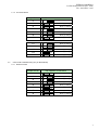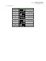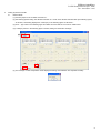
1
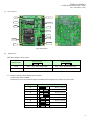
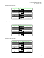
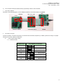
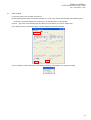
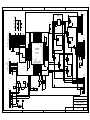
FEBL610Q359RB-01
LAPIS Semiconductor CO., LTD.
Dec. 2012 (Rev. 1.00)
ML610Q359/ML610Q360 Reference Board User's Manual
ML610Q359/ML610Q360 Reference board is prepared by LAPIS Semiconductor to have you study the operations of
ML610Q359/ML610Q360.
The board is arranged so that necessary components are mounted by you according to your purpose, then only minimum necessary
components are mounted on the board by LAPIS Semiconductor for brief use of ML610Q359/ML610Q360.
By using the board with "uEASE on-chip debug emulator" (hereinafter referred to "uEASE") and "free sample U8 Development Tools
CD-ROM" which is bundled in the package of uEASE not only Software development/debugging but also writing Flash ROM in the
devices are capable.
This board also works in stand alone mode with external power suppy without uEASE.
Before starting works with this board, read below carefully and understand notices.
A)
The board features
Incorporates ML610Q359/ML610Q360 or 64pin IC-Socket
Supports flash ROM programming and on-chip debugging (using TEST0 and TEST1_N pins)
High extendibility; Through-holes for your peripheral board are equipped with microcontroller pins
The power supply used can be selected ( uEASE or peripheral board )
Prepared the pad to mount parts ( parts necessary for microcontroller operation )
The connector connectable to SDCB2 is carried. The program of the sound data to built-in P2ROM/external FLASH is possible
using SDCB2.
Please refer to G) for the connection method of SDCB2 and the program/verify method of the sound data to built-in
P2ROM/external FLASH.
B)
The board hardware specifications
Please refer to the reference schematics for detail on connections of each hardware parts.
Embedded microcontroller
U1: 64pin IC socket for ML610Q359/ML610Q360
PWR: Jumper for input power supply switch ( 3pin pin-header and short pin )
AOUT: Connection switch of a LINE output and a speaker amplifier analog input
( 3pin pin header and a short pin)
J1-J8: The jumper for rewriting of Built-in P2ROM/External FLASH by CNSDCB2 ( 3pin pin header
and a short pin) ( 8 pieces )
RESET_SW: Reset switch for M25PE16
SPEAKER: Jack for speaker connection
R1 – R3: Resistance for light emitting diodes (P20-P22)
R4: Pull-up resistance for RESET_N
Embedded parts
R7: Pull-up resistance for W/ port of M25PE16
P20 - P22: Light emitting diodes
CNUE: Connector for on-chip debug emulator
( 14pin connector )
CNSDCB2: Conector for Sound Device Control Board2( SDCB2) ( 14pin connector )
C4, C7 - C13: Capacitors for power supply ( 8 pieces )
C5-C6: Capacitors for XTAL( 2pieces )
C14: Capcitors for reset of M24PE26 ( 1piece )
XT: 32.768kHz oscillator ( 1piece )
FLASH: M25PE16(1piece)
Pads for mounting
C1 -C3: Capacitors for SA-ADC input voltage connection (3 pieces)
CN1 - CN4: Pads for peripheral board connectors
(10pin x 1, 16pin x 1, 18pin x 1, 14pin x 1, 2.54mm pitch )
J9 – J11: Land for light emitting diodes (P20-P22)
R5 – R6: Pads for opening or short
Other useful pads
DVDD, DVSS, AVDD, AVSS, AIN0 – AIN2
Operating voltage
+2.2V to +3.6V
Board size
80.00 x 100.00 mm
1
FEBL610Q359RB-01
LAPIS Semiconductor CO., LTD.
Dec. 2012 (Rev. 1.00)
C)
P ar ts la you t
J1-J8
CN2
FLASH
CNSDCB2
CN3
CN1
PWR
AOUT
1pin
CNUE
P20-P22
SPEAKER
CN4
<fig.1 Parts layout>
D)
Jumper set up
PWR, AOUT jumper is set as follows.
Short (1) and (2)
Short (2) and (3)
(1) (2) (3)
(1) (2) (3)
PWR
USR:Use of user’s power supply
SYS:Use of uEASE power supply
AOUT
SPIN:Use of internal speaker amplifier
LINE:Use of external speaker amplifier
Jumper Pin No.
J1−J8 jumpers shall be used by default status as follows.
Program/Verify built-in P2ROM
Please refer to G) for the connection method of SDCB2 and the program/verify method of the sound data.
Jumper Pin No.
The condition of connection
J1
(1) (2) (3)
Short (1) and (2)
J2
(1) (2) (3)
Short (2) and (3)
J3
(1) (2) (3)
Short (2) and (3)
J4
(1) (2) (3)
Short (2) and (3)
J5
(1) (2) (3)
Short (1) and (2)
J6
(1) (2) (3)
Short (1) and (2)
J7
(1) (2) (3)
Short (1) and (2)
J8
(1) (2) (3)
Short (1) and (2)
2
FEBL610Q359RB-01
LAPIS Semiconductor CO., LTD.
Dec. 2012 (Rev. 1.00)
Read built-in P2ROM data by MCU
Jumper Pin No.
The condition of connection
J1
(1) (2) (3)
Short (2) and (3)
J2
(1) (2) (3)
Short (2) and (3)
J3
(1) (2) (3)
Short (2) and (3)
J4
(1) (2) (3)
Short (2) and (3)
J5
(1) (2) (3)
Short (1) and (2)
J6
(1) (2) (3)
Short (1) and (2)
J7
(1) (2) (3)
Short (2) and (3)
J8
(1) (2) (3)
Short (1) and (2)
Program/Verify external FLASH
Please refer to G) for the connection method of SDCB2 and the program/verify method of the sound data.
Jumper Pin No.
The condition of connection
J1
(1) (2) (3)
Short (1) and (2)
J2
(1) (2) (3)
Short (1) and (2)
J3
(1) (2) (3)
Short (1) and (2)
J4
(1) (2) (3)
Short (1) and (2)
J5
(1) (2) (3)
Short (2) and (3)
J6
(1) (2) (3)
Short (2) and (3)
J7
(1) (2) (3)
Short (2) and (3)
J8
(1) (2) (3)
Short (2) and (3)
*Please write data in external FLASH without setting a device to a socket.
Read external FLASH data by MCU
Jumper Pin No.
The condition of connection
J1
(1) (2) (3)
Short (2) and (3)
J2
(1) (2) (3)
Short (2) and (3)
J3
(1) (2) (3)
Short (2) and (3)
J4
(1) (2) (3)
Short (2) and (3)
J5
(1) (2) (3)
Short (2) and (3)
J6
(1) (2) (3)
Short (2) and (3)
J7
(1) (2) (3)
Short (2) and (3)
J8
(1) (2) (3)
Short (2) and (3)
3
FEBL610Q359RB-01
LAPIS Semiconductor CO., LTD.
Dec. 2012 (Rev. 1.00)
E)
Notes on use
(1) The information contained herein can change without notice owing to product and/or technical improvements.
Before using the product, please make sure that the information being referred to is up-to-date.
(2) Before using this board, read carefully and understand the contents of the ML610Q359/ML610Q360 user's manual and the uEASE
user's manual.
(3) The engineering sample of ML610Q359/ML610Q360 might be mounted on the board.
Therefore, please confirm the characteristic finally by using MP of ML610Q359/ML610Q360 and customer's mass production
boards.
(4) LAPIS Semiconductor will not provide any support for this board, but the board can be exchanged with a new product only when it
has an initial failure.
(5) Notes when the PWR jumper is set to USR side and the uEASE is connected.
Turn on the power supply of the peripheral board after starting the uEASE..
Moreover, Stop the uEASE after turning off the power supply of the peripheral board.
(6) When the PWR jumper is set to the uE side, the ability to supply power of the uEASE is +3.3v/100mA.
(7) Notes when the RESET_N signal is prepared on the peripheral board side.
If you use the uEASE, open or set DVDD-level RESET_N signal pin (CN1_1pin).
(8) There is a possibility of short the circuit when using it on electro conductive so that the board may have the pattern on the solder
side.
Therefore, please use the board on nonconductivity or put the protection parts on the solder side if necessary.
(9) When you use SA-ADC:
Please mount noise decrease capacitor (C1 - C3) for AIN0 – AIN2 if necessary when you select the use of AIN0 – AIN2 (without
using CN2) on the board. (Refer to fig.4.)
AVDD is wired with DVDD through R5. Please cut the short pattern of the R5 when you use AVDD, as shown in the fig.3.
AVSS is wired with DVSS through R6. Please cut the short pattern of the R6 when you use AVSS, as shown in the fig.3.
(10) When you don’t use light emitting diodes:
P20-P22 can drive direct to light emitting diodes. P20-P22 are wired with light emitting diodes through J9 – J11.
Please cut the land of the J9 – J11 when you don’t use light emitting diodes, as shown in the fig.2.
(11) The following parts are mounted on the board:
C4, C7-C11, CNUE, CNSDCB2, R4-R7, P20-P22, XT, RESET_SW, SPEAKER, PWR, AOUT, U1 (64pin IC socket)
(12) The following parts are not mounted on the board:
C1-C3, CN1-CN4
4
FEBL610Q359RB-01
LAPIS Semiconductor CO., LTD.
Dec. 2012 (Rev. 1.00)
Cut Land
Top View
Cut Pattern
<fig.2 P20-P22 Light emitting diodes>
Cut Land
Cut Pattern
Top View
<fig.3 AVDD,AVSS>
Top View
C1-C3
<fig.4 AIN0-AIN2 (SA-ADC)>
5
FEBL610Q359RB-01
LAPIS Semiconductor CO., LTD.
Dec. 2012 (Rev. 1.00)
F)
The connection method of SDCB2 and the program/verify method of the sound data
1
Connection of Board
As shown in the following figure, connect Reference Board, Connection board, and SDCB2.
CNSDCB2
J1~J8
Reference Board
2
CN2
J1~J7,
J11~J15
CN1
Connection Board
CN4
SDCB2
Connection of Jumper
Connect the jumper of a reference board and a connection board as follows, respectively. In addition, perform the change of a jumper
after plug out a power cable and a USB cable.
2.1
Case of external Flash writing
2.1.1 Reference board
Jumper Pin No.
The condition of connection
J1
(1) (2) (3)
Short (1) and (2)
J2
(1) (2) (3)
Short (1) and (2)
J3
(1) (2) (3)
Short (1) and (2)
J4
(1) (2) (3)
Short (1) and (2)
J5
(1) (2) (3)
Short (2) and (3)
J6
(1) (2) (3)
Short (2) and (3)
J7
(1) (2) (3)
Short (2) and (3)
J8
(1) (2) (3)
Short (2) and (3)
*Please write data in external Flash without setting a device to a socket.
6
FEBL610Q359RB-01
LAPIS Semiconductor CO., LTD.
Dec. 2012 (Rev. 1.00)
2.1.2 Connection Board
Jumper Pin No.
2.2
The condition of connection
J1
(1) (2) (3)
Short (2) and (3)
J2
(1) (2) (3)
Short (1) and (2)
J3
(1) (2) (3)
Short (1) and (2)
J4
(1) (2) (3)
Short (2) and (3)
J5
(1) (2) (3)
Short (2) and (3)
J6
(1) (2) (3)
Short (2) and (3)
J7
(1) (2) (3)
Short (1) and (2)
J11
(1) (2) (3)
Short (2) and (3)
J12
(1) (2) (3)
Short (2) and (3)
J13
(1) (2) (3)
Short (2) and (3)
J14
(1) (2) (3)
Short (1) and (2)
J15
(1) (2) (3)
Short (1) and (2)
Case of built-in P2ROM writing (only for ML610Q360)
2.2.1 Reference board
Jumper Pin No.
The condition of connection
J1
(1) (2) (3)
Short (1) and (2)
J2
(1) (2) (3)
Short (2) and (3)
J3
(1) (2) (3)
Short (2) and (3)
J4
(1) (2) (3)
Short (2) and (3)
J5
(1) (2) (3)
Short (1) and (2)
J6
(1) (2) (3)
Short (1) and (2)
J7
(1) (2) (3)
Short (1) and (2)
J8
(1) (2) (3)
Short (1) and (2)
7
FEBL610Q359RB-01
LAPIS Semiconductor CO., LTD.
Dec. 2012 (Rev. 1.00)
2.2.2 Connection Board
Jumper Pin No.
The condition of connection
J1
(1) (2) (3)
Short (1) and (2)
J2
(1) (2) (3)
Short (2) and (3)
J3
(1) (2) (3)
Short (1) and (2)
J4
(1) (2) (3)
Short (2) and (3)
J5
(1) (2) (3)
Short (2) and (3)
J6
(1) (2) (3)
Short (2) and (3)
J7
(1) (2) (3)
Short (1) and (2)
J11
(1) (2) (3)
Short (1) and (2)
J12
(1) (2) (3)
Short (1) and (2)
J13
(1) (2) (3)
Short (1) and (2)
J14
(1) (2) (3)
Short (2) and (3)
J15
(1) (2) (3)
Short (2) and (3)
8
FEBL610Q359RB-01
LAPIS Semiconductor CO., LTD.
Dec. 2012 (Rev. 1.00)
3
Writing by Board Controller
3.1
External Flash
(1) Set each jumper to the condition of Section 2.1.
(2) After starting Speech Utility, click "Board Controller" in a “Tools” menu. Board controller starts (The following figure).
At this time, check being displayed on “Device(A)” in the following figure as “ML22420.”
(3) Click “…(B)” button in the following figure and select the sound data of a S format or a BIN format.
(4) If “Write(C)” button in the following figure is clicked, writing and verification will begin.
(A)
(C)
(B)
(5) The message of “Write Completed!” will be displayed if writing and verification are completed normally.
9
FEBL610Q359RB-01
LAPIS Semiconductor CO., LTD.
Dec. 2012 (Rev. 1.00)
3.2
Built-in P2ROM
(1) Set each jumper to the condition of Section 2.2.
(2) After starting Speech Utility, click "Board Controller" in a “Tools” menu. Board controller starts (The following figure).
At this time, check being displayed on “Device(A)” in the following figure as “ML22(P)826.”
(3) Click “…(B)” button in the following figure and select the sound data of a S format or a BIN format.
(4) If “Write(C)” button in the following figure is clicked, writing and verification will begin.
(A)
(C)
(B)
(5) The message of “Write Completed!” will be displayed if writing and verification are completed normally.
10
A
C
B
DL
CN3
CN18P
XTAL
2
2 1
PIN16
CSB
RESET_N
SO
SI
SCK
WB
C6 10PF
1
2
1
2
C5 10PF
VPP
VCC2
A
1
2
3
4
5
6
7
8
9
10
11
12
13
14
DVSS
TEST1_N
PIN4
TEST0
PIN3
LAPIS SEMICONDUCTOR CO.,LTD
AVSS
1
1
VCC1
DVSS
1 R6 2 0
DVSS
C2 1
C3 1
3
CNSDCB2
CN14P
ML610Q359/360 Reference Board
APPLICATION
UVDD
2
2
1UF
2 1
C9
NML
TITLE
DVSS
P04
P05
P30
P31
P32
P33
P34
P35
P36
P37
VDDR
AIN0
AIN1
AIN2
AVDD
AVSS
AVSS
1
PIN15
PIN14
2 1
C8 0.1UF
PIN11
2 1
C7 10UF
360 PRG
2
2 1
C10 1UF
48
47
46
45
44
43
42
41
40
39
38
37
36
35
34
33
P10
P53
P52
P51
P50
P47
P46
P45
P44
TESTO2
P43
P42
P41
P40
P56/TESTO5
P55/TESTO4
SPM
SPP
TEST0
TEST1_N
RESET_N
P54/TESTO3
P57/TESTO6
NC/PVPP
P60
P61
VDDL
DVDD
DVSS_13
VDDX
XT1
XT0
1
2
3
4
5
6
7
8
9
10
11
12
13
14
15
16
PIN1
PIN2
PIN3
PIN4
PIN5
PIN6
PIN7
PIN8
PIN9
PIN10
PIN11
PIN12
PIN13
PIN14
PIN15
PIN16
C1 1
PIN48
PIN47
PIN46
PIN45
PIN44
PIN43
PIN42
PIN41
PIN40
PIN39
PIN38
PIN37
PIN36
PIN35
PIN34
PIN33
PIN50
PIN49
1
2
C12 1UF
1
2
C11 0.1UF
NML
PVPP
1
MJ-354A0
DVSS
NML
2
RK73K2A
1 1
2
R1 270
LED
2 2
1 J9
2
A2-3PA-2_54DSA
1
3
1
2
C4 10UF
PIN2
U3
T 3
B 2
S 1
C14 1UF
RK73K2A
1 1
2
R2 270
LED
2 2
1 J10
1
2
PIN1
360 PRG
1
2
3
4
5
6
7
8
9
10
11
12
13
14
15
16
1
RK73K2A
1 1
2
R3 270
LED
2 2
1 J11
A2-3PA-2_54DSA
1
3
2 0
J7
A2-3PA-2_54DSA
1
3
R5
P54
2
1
2
3
4
5
6
7
8
9
10
11
12
13
14
1
PIN6
J6
A2-3PA-2_54DSA
1
3
SYS
AVDD
2
PWR
CNUE
CN14P
AVDD
DVDD
P57
PIN[64:1]
XT
DVSS
FLASH PRG
FLASH
PIN7
DVDD
DVSS
DVDD
DVSS
360
PIN34 P56
PIN33 P55
PIN8 PVPP
DVSS
USR
4
DVSS
DVSS
3
2
U1
2
1
3
RESET_SW
PUSHSW
J3
A2-3PA-2_54DSA
1
3
PIN14
64PIN TQFP
IC_SOCKET
32
31
30
29
28
27
26
25
24
23
22
21
20
19
18
17
1
CN2
CN16P
PIN17
PIN18
PIN19
PIN20
PIN21
PIN22
PIN23
PIN24
PIN25
PIN26
PIN27
PIN28
PIN29
PIN30
PIN31
PIN32
DVSS
NML/RST
2
PIN9
PIN10
PIN11
ML610Q359
ML610Q360
AVSS
AVDD
AIN2
AIN1
AIN0
VDDR
P37
P36
P35
P34
P33
P32
P31
P30
P05
P04
P55/TSTO4
P56/TSTO5
P40
P41
P42
P43
TESTO2
P44
P45
P46
P47
P50
P51
P52
P53
P10
P62
P63
360 PRG
NML
AVSS
PIN32
PIN31
PIN30
PIN29
PIN28
PIN27
PIN26
PIN25
PIN24
PIN23
PIN22
PIN21
PIN20
PIN19
PIN18
PIN17
1
2
3
4
5
6
7
8
9
10
11
12
13
14
15
16
17
18
NML
J5
A2-3PA-2_54DSA
1
3
PIN62
1 2
C13
FLASH PRG
2
0.022UF
PIN5
PIN6
PIN7
1
2
3
4
5
6
7
8
9
10
AVDD
J8
A2-3PA-2_54DSA
1
3
CN1
CN10P
P60
P61
VDDL
EXDVDD
DVSS
VDDX
PIN61
SPIN
FLASH PRG
PIN5 RESET_N
2
LINE
P62
P63
NMI
P20
P21
P22
DVSS_55
P00
P01
P02
P03
SG
AOUT
SPIN
SPVDD
SPVSS
DVDD
NML
2
AOUT
49
50
51
52
53
54
55
56
57
58
59
60
61
62
63
64
PIN51
PIN52
PIN53
PIN54
PIN55
PIN56
PIN57
PIN58
PIN59
PIN60
PIN61
PIN62
PIN63
PIN64
8
7
6
5
J2
A2-3PA-2_54DSA
1
3
PIN63
PIN64
DVSS DVSS
RESET_N
P54/TSTO3
P57/TSTO6
DVDD
VCC
RST/
C
D
DVSS
2
SPVDD
SPVSS
PIN51
PIN52
PIN53
PIN54
PIN55
PIN56
PIN57
PIN58
PIN59
PIN60
1
2
3
4
5
6
7
8
9
10
11
12
13
14
S/
Q
W/
VSS
PRG
J4
A2-3PA-2_54DSA
1
3
2
P20
R4 10K
NMI
P20
P21
P22
DVSS
P00
P01
P02
P03
SG
AOUT
P21
1
2
3
4
DVDD
RK73K2A
1
2
CN4
CN14P
P22
SOP8
U2
J1
A2-3PA-2_54DSA
1
3
1
PIN33
PIN34
PIN35
PIN36
PIN37
PIN38
PIN39
PIN40
PIN41
PIN42
PIN43
PIN44
PIN45
PIN46
PIN47
PIN48
PIN49
PIN50
M25PE16
RK73K2A
1
2
R7 10K
DVDD
ML610Q355/ML610Q360
DWG NO
DRAWN By
AVSS
B
C
QTS-11544
SHEET
1 of 1
D
REV
1.00
4
5.5
94.5
81.28
33.02
4-φ3.6
2.54
1
14
2
SYS
1
13
14
2
PWR
13
CNSDCB2
2
USR
SPIN
XT
10
SPVSS
SVVDD
P33
AOUT
P34
SG
P03
P35
P36
53.34
14
▼1
P02
IC SOCKET
P37
P01
VDDR
P00
AIN0
AIN1
1 2 3
DVSS
P22
AIN2
P21
AVDD
CN4
P20
1
12.7
P63
P62
P10
P53
P52
P50
P51
P46
P47
P44
CN3
P45
P43
TESTO2
P41
P42
NMI
P40
2.54
12.7
1
P55/TSTO4
P56/TSTO5
M25EP16
AVSS
16
18
15.24
27.94
96.52
100
P20
P21
P22
74.93
P31
P32
ML610Q359/360 Reference Borad
65
J1-8
P54/TSTO3
RESET_N
P57/TSTO6
P60
VDDL
P61
EXDVDD
P30
80
3
1
VDDX
DVSS
CN2
P05
QTU-11643
CN1
1
AOUT
+
1
P04
SPEAKER
CNUE
LINE
RESET_SW