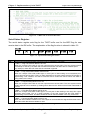
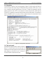
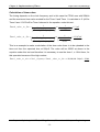
1
Honours Project FPGA Implementation of a Simple Microprocessor Napier University Edinburgh BGEPB1 MicroController for Spartan-3 PFGA Title Page NAME: Benjamin Grydehoej MATRICULATION NO.: 04007714 UNIVERSITY: Napier University Edinburgh EDUCATION: BEng (Honours) Electronic and Computer Engineering MODULE TITLE: BEng Honours Project MODULE NO.: SE42201 PROJECT TITLE: FPGA Implementation of a Simple Microprocessor SUPERVISOR: Dr. Thomas David Binnie SUBMISSION DATE: 5/5/2006 Benjamin Grydehoej (04007714) – BEng (Honours) Electronic and Computer Engineering -2- Abstract This report covers implementation of a simple 8-bit microprocessor in a FPGA, the design is made as an emulated standard 8051 microcontroller. It is build based on the free PicoBlazeTM IP Core from Xilinx, containing a Special Function Register which is specifically chosen for this microcontroller. BGEPB1 is short for (BG-Electronic PicoBlaze version 1). The microcontroller is implemented with parallels input and output ports (I/O ports), serial UART, timers and interrupts. The microcontroller interface is programmed in VHDL and the test programs for the microcontroller are made in C-code language using the PCCOMP compiler by Francesco Poderico. Tested in both ModelSim, a simulating tool, and in practical on the development board named Spartan-3 starter kit from Xilinx using the FPGA XC3S200. The second part of the report is regarding the design of a CAN bus hardware interface for the development board and a CAN VHDL interface for transmitting data through the CAN bus level converter out on to the CAN bus. The last part of the report is a setup guide for the software used to implemented and design new VHDL function. Benjamin Grydehoej (04007714) – BEng (Honours) Electronic and Computer Engineering -3- Acknowledgement I thank the following individuals for their contribution of PicoBlaze microcontroller Core and Development tool there are used for this project. • Ken Chapman, Xilinx Ltd. Benchmark House PicoBlazeTM core and Serial UART • Xilinx Inc. ISE Service Pack • Model Technology, a Mentor Graphics Corporation ModelSim XE II/Starter • Francesco Poderico PCCOMP PicoBlaze C Compiler Benjamin Grydehoej (04007714) – BEng (Honours) Electronic and Computer Engineering -4- Table of Contents Title Page....................................................................................................................... 2 Abstract.......................................................................................................................... 3 Acknowledgement .......................................................................................................... 4 Table of Contents........................................................................................................... 5 Chapter 1: Introduction 1.1. About the project.......................................................................................................................7 1.2. Aim of the project .....................................................................................................................7 1.3. Project description.....................................................................................................................8 1.4. Requirement specification.........................................................................................................9 1.5. Problem solution .....................................................................................................................10 1.6 Time-Plan.................................................................................................................................11 Chapter 2: Implementation of PicoBlazeTM with I/O ports interface 2.1. Introduction.............................................................................................................................12 2.2. Background of PicoBlazeTM....................................................................................................12 2.3. Implementation of core and Parallel I/O with interrupts ........................................................14 2.5. VHDL code for the I/O Ports interface...................................................................................15 Reset to standard value: .............................................................................................................15 Write and Read to I/O ports: ......................................................................................................16 Interrupt System:........................................................................................................................17 2.6. Test software in C code...........................................................................................................20 2.7. Simulation ...............................................................................................................................21 2.8. Test and result .........................................................................................................................22 Chapter 3: Implementation of serial UART 3.1. Introduction.............................................................................................................................23 Specification: .................................................................................................................................23 3.2. Implementation of serial UART .............................................................................................24 Read and write to UART: ..........................................................................................................25 BAUD Rate Timing: ..................................................................................................................26 Serial Status Register: ................................................................................................................27 3.3. Simulation ...............................................................................................................................28 3.4. Test and result .........................................................................................................................28 Chapter 4: Implementation of Timers 4.1. Introduction.............................................................................................................................29 4.2. Implementation of Timers.......................................................................................................29 Timer Register: ..........................................................................................................................31 Calculation of timer value:.........................................................................................................32 4.3. Simulation ...............................................................................................................................33 4.4. Test and result .........................................................................................................................34 Chapter 5: Implementation of Serial Flash ROM interface 5.1. About serial interface ..............................................................................................................35 Benjamin Grydehoej (04007714) – BEng (Honours) Electronic and Computer Engineering -5- Chapter 6: Design of CAN-BUS Interface 6.1. Introduction.............................................................................................................................36 6.2. Design of CAN-BUS Hardware Interface ..............................................................................38 6.3. Design of CAN-BUS VHDL interface for transmitting .........................................................40 6.4. Simulation ...............................................................................................................................42 6.4. Simulation ...............................................................................................................................42 6.5. Test and result .........................................................................................................................42 Chapter 7: Software Setup 7.1. Introduction.............................................................................................................................43 7.2. Setup of C and ASM Compiler ...............................................................................................43 7.3. Simulation in ModelSim .........................................................................................................45 7.4. Download to FPGA via iMPACT tool....................................................................................46 Chapter 8: Conclusion .......................................................................................... 48 Related Materials and References References:.................................................................................................................................49 Bibliography: .............................................................................................................................49 Software: ....................................................................................................................................49 Appendix A: The VHDL code for I/O Interface..................................................................................................50 Appendix B: Special Function Register (BGEPB1.h).........................................................................................55 Appendix C: Pin Option for FPGA and Development board..............................................................................56 Benjamin Grydehoej (04007714) – BEng (Honours) Electronic and Computer Engineering -6- Chapter 1: Introduction Napier University Edinburgh Chapter 1 Introduction 1.1. About the project A microcontroller in a Field-Programmable Gate Array (FPGA) is not world news, but a free 8051 emulate core in a FPGA is not available on the marked at the moment. There is an embedded microcontroller core on the market at the moment which matches the project, though without Control Area Network (CAN) bus Interface. It is the PB8051 Xilinx AllianceCORETM[1] to the price of $ 495.95. The embedded microprocessor cores for FPGA is split up in Hard-core and Soft-core processors, a Hard-core Processor is the IBM PowerPCTM 405 32-Bit RISC processor which run on Xilinx Virtex-II Pro and Virtex-4. The Soft-core processor is a MicroBlazeTM 32-bit RISC core which runs up to 180MHz in a Virtex-4 with 166 MIPS build for complex systems, networking, telecommunication, data communication and embedded systems. All these microprocessor cores need a license to be used in a product. Another free soft-core processor from Xilinx is the PicoBlazeTM core which is an 8-Bit RISC processor this can be implemented on Virtex™ and Spartan™ series of FPGAs and CoolRunner™-II CPLDs. This microprocessor is the one chosen for this project because it is free and makes it possible to run in a low cost Spartan 3 FPGA. The purpose of this project is to make a cheap microcontroller core with peripherals like an 8051 standard microcontroller plus a CAN bus interface that makes it possible to customize the core for special projects. 1.2. Aim of the project The aim for this project is to get know-how about FPGA and Very High Spe/ed Integrated Circuit Hardware Description Language (VHDL), and to integrated PicoBlazeTM processor in the Spartan-3 FPGA with Input and Output for parallel and serial interfaces and finally simulate and test the project in practical. Benjamin Grydehoej (04007714) – BEng (Honours) Electronic and Computer Engineering -7- Chapter 1: Introduction Napier University Edinburgh 1.3. Project description The block diagram in figure 1.1 shows the upcoming design of an emulated 8051 microcontroller, consisting of the Xilinx PicoBlazeTM microprocessor, with a instruction Read Only Memory (ROM) which makes it possible to run machine code from the ROM, generate by assembly or C code compiler. The machine code for the Instruction ROM is uploaded via the Xilinx program called Project navigator, using the iMPACT tool. The machine code is uploaded with the VHDL code for the project via Joint Test Action Group (JTAG). The size of the Instruction ROM is only 1K x 16 and very small and will only be used as a Boot or Monitor ROM with all necessary information for communication to the peripherals, for more external ROM space available in the serial Flash which communicates via serial data control by the Serial Flash ROM interface Block. FPGA JTAG Boot Rom Instruction Code 1K x 16 CAN Bus UART Timer Serial Flash Rom Interface JTAG Special Function Register Watchdog Timer System Clock 8051 Emulation Peripherals Serial UART Internal Address/Data and Control Bus PicoBlaze Core Reset CLK (50MHz) EA WR RD PSEN Control Address Decoder I/O PORTS Data[7:0] ADD[15:0] P1[7:0] P3[7:0] P4[7:0] P5[7:0] Serial Flash Rom Platform Flash Figure 1.1 – Block diagram over BGEPB1 Emulated 8051 Microcontroller Benjamin Grydehoej (04007714) – BEng (Honours) Electronic and Computer Engineering -8- Chapter 1: Introduction Napier University Edinburgh 1.4. Requirement specification The specification for the project is described in this paragraph and all the special function calls are made out from the list for Special Function Register (SFR) showed in table 1.1. The project consists of building an embedded microcontroller in a FPGA with a CAN-Bus interface shown in the block diagram at page 8 figure 1.1. The specification of the project is listed in bullets point under this text. • PICOBLAZETM CORE AND BOOT ROM (Use the PicoBlazeTM features showed on page 13) • SERIAL UART (RS232) (Standard configuration 1 start bit, 8 data bit, no parity and 1 stop bit) • CAN BUS UART (Designed to ISO 11898-1, CAN 2.0A & B, support bit rates up to 1Mbit/s) • TIMER (Timer 0 as 8-bit Timer and Timer 1 as 16-bit Timer) • SERIAL FLASH ROM INTERFACE (Controller interface or extern serial program store up to 2Mbit) • SPECIAL FUNCTION REGISTER (SFR) (The SFR control all the call to ports, serial UART, Timer etc.) • WATCHDOG TIMER (Automatics reset of the microcontroller with problems in the code) • SYSTEM CLOCK (Standard option is 50MHz, run up to 200MHz or 100MIPS in a Virtex-II Pro FPGA) • CONTROL (Control signal for external Rom and RAM or other peripherals components) • ADDRESS DECODER (Address bus expander up to 16 bit wide) • I/O PORTS (Port 0, 1, 3, 4 and 4 with external interrupts and Serial RS232 and CAN interface) Symbol: P0 P1 P2L P2H P3 P4 P5 SBUF TLBS THBS SCON IEN0 IEN1 ISC0 TCON TC0 TCL1 TCH1 Name: Port 0 Port 1 Port 2 (Address Bus low byte “the lower 8-bit part of 16-bit”) Port 2 (Address Bus high byte “the higher 8-bit part of 16-bit”) Port 3 Port 4 Port 5 Serial channel buffer register Timer Low BAUE Rate Serial (Low byte part of 16-bit) Timer High BAUE Rate Serial (High byte part of 16-bit) Serial channel control register Interrupt enable register 0 Interrupt enable register 1 Interrupt service control register Timer service control register Timer Count 0 (8-bit) Timer Count Low 1 (part of 16-bit) Timer Count Low 1 (part of 16-bit) Address: HEX 01 HEX 02 HEX 03 HEX 04 HEX 05 HEX 06 HEX 07 HEX 08 HEX 09 HEX 0A HEX 0B HEX 0C HEX 0D HEX 0E HEX 0F HEX 10 HEX 11 HEX 12 Table 1.1 – List over Special Function Register. Benjamin Grydehoej (04007714) – BEng (Honours) Electronic and Computer Engineering -9- Chapter 1: Introduction Napier University Edinburgh 1.5. Problem solution The task concerns the building an embedded microcontroller in a FPGA with a CAN bus interface from the requirement specifications at page 9. The microprocessor used for this project is the Xilinx PicoBlazeTM microprocessor core and the task is to implement parallel Input/Output port interfaces with Interrupts, serial UART, Timer and a CAN BUS interface. It can be necessary to implement the VHDL code giving access to the Serial Flash ROM for more program space. The PicoBlazeTM core, the Instruction ROM and the serial UART is VHDL code which will be downloaded as free IP Core available from Xilinx.com homepage. The rest of the blocks in the block diagram in figure 1.1 at page 8, are functions of VHDL code constructed from scats. The process for the project will be implementation of the PicoBlazeTM core with Boot ROM and Serial UART and create and implemented an Input/output interface with Interrupt control. Two different timers, a Timer 0 using an 8-bit counter and a Timer 1 which uses a 16-bit counter. The last unit there will be create and implemented is the CAN bus UART which also will be build from nothing. All the functions will be controlled by the Special Function Register showed in table 1.1 at page 9. Benjamin Grydehoej (04007714) – BEng (Honours) Electronic and Computer Engineering - 10 - Chapter 1: Introduction Napier University Edinburgh 1.6 Time-Plan Benjamin Grydehoej (04007714) – BEng (Honours) Electronic and Computer Engineering - 11 - Chapter 2: Implementation of PicoBlazeTM with I/O ports interface Napier University Edinburgh Chapter 2 Implementation of PicoBlazeTM with I/O ports interface 2.1. Introduction This chapter descripts the PicoBlaze core and its features for the processor and how to implement the microcontroller core in a Spartan-3 FPGA with parallel Inputs and Outputs and interrupt service controller for external interrupt at I/O pins. This chapter will cover all the steps from the design of I/O ports VHDL code and set the Xilinx project navigator up and make a C language test program for the I/O ports to test the system in hardware. 2.2. Background of PicoBlazeTM The PicoBlaze microcontroller is a compact core, making it possible to download free version without IP license from Xilinx.com after registration of user. The microcontroller is an embedded 8-bit RISC core optimized for the Spartan-3, Virtex-II, and Virtex-II Pro FPGA families. The PicoBlaze microcontroller is optimized for efficiency and low development cost. It occupies just 96 FPGA slices, or 12,5% of an XC3S50 FPGA, and performs a respectable 44 to 100 million instructions per second (MIPS). For development on the PicoBlaze microcontroller the tool named Xilinx project navigator version 6.3.03 is used. This is a free software from Xilinx ready to download at Xilinx.com and makes it possible to add I/O ports, serial UART, timer, etc. To make C language test software for the microprocessor there are used two compilers one from Francesco Poderico’s named PCCOMP, a DOS version, which compile the C language code to ASM code written in notepad. The second compiler is from Xilinx and named KCPSM3 which compile the ASM code to VHDL and making it ready to download to the FPGA after complete compiling of the project in the Xilinx project navigator. Benjamin Grydehoej (04007714) – BEng (Honours) Electronic and Computer Engineering - 12 - Chapter 2: Implementation of PicoBlazeTM with I/O ports interface Napier University Edinburgh Features: The block diagram in figure 2.1 show the PicoBlaze microcontrollers supports the following features.[2] • 16 byte-wide general-purpose data registers • 1K instructions of programmable on-chip program store, automatically loaded during FPGA configuration • Byte-wide Arithmetic Logic Unit (ALU) with CARRY and ZERO indicator flags • 64-byte internal scratchpad RAM • 256 input and 256 output ports for easy expansion and enhancement • Automatic 31-location CALL/RETURN stack • Predictable performance, always two clock cycles per instruction, up to 200 MHz or 100 MIPS in a Virtex-II Pro FPGA • Fast interrupt response; worst-case 5 clock cycles • Optimized for Xilinx Spartan-3, Virtex-II, and Virtex-II Pro FPGA architectures just 96 slices and 0.5 to 1 block RAM • Assembler, instruction-set simulator support Figure 2.1 – PicoBlaze embedded microcontroller Block Diagram Benjamin Grydehoej (04007714) – BEng (Honours) Electronic and Computer Engineering - 13 - Chapter 2: Implementation of PicoBlazeTM with I/O ports interface Napier University Edinburgh 2.3. Implementation of core and Parallel I/O with interrupts The block diagram in figure 2.2 show the PicoBlaze connected with instruction ROM and the I/O interface for read and writes 8-bit’s values (HEX 00 - FF) to the ports P0, P1, P3, P4 and P5 and write 16-bit’s addressed (HEX 0000 - FFFF) out to port 2 compared with the purple I/O ports block and blue address decoder block at the BGEPB1 emulation 8051 peripherals block respectively in the diagram in figure 1.1 page 8. The system is created with three external interrupt pins at port 1 to receive external interrupts from hardware, example a keyboard switch or some other hardware inputs. The PicoBlaze processor core communicate to the Input/Output Ports block (I/O block) via OUT_PORT which is an 8-bit data transmit out of the microcontroller in an internal pipeline to the I/O block. To receive data the internal pipeline IN_PORT is used which receive 8-bit data value from the I/O block. The PORT_ID is the port identity to chose the right channel for read or write via the internal pipeline, it is possible to control up to 256 I/O ports. Figure 2.2 – Block diagram over I/O interface Benjamin Grydehoej (04007714) – BEng (Honours) Electronic and Computer Engineering - 14 - Chapter 2: Implementation of PicoBlazeTM with I/O ports interface Napier University Edinburgh 2.5. VHDL code for the I/O Ports interface The VHDL code is program in Xilinx project navigator, made from the BGEPB1 Special Function Register (SFR) shown in the requirement specifications in chapter 1.4 table 1.1 at page 9. The complete code is shown in appendix A page 50, under this text there are a cut-out of the reset routines from the I/O interface code. Reset to standard value: This code show the value of the I/O ports after reset where all ports will be set to high impedance level or synthesizable tri-state buffer. The Address bus is set to Hexadecimal 0000 this means the address bus will point on the memory at address 0, the maximum size of addressable memory will be 216 = 65336 or 64Kbyte. Figure 2.3 – VHDL code for reset data value for I/O interface to default. Benjamin Grydehoej (04007714) – BEng (Honours) Electronic and Computer Engineering - 15 - Chapter 2: Implementation of PicoBlazeTM with I/O ports interface Napier University Edinburgh Write and Read to I/O ports: The I/O interface code looks at the Read- or Write-enable input and the ID input and uses Data-in and Data-out for transmit and receive data from this unit. As an example for transmit data to Port 0 also called DataBus, the programe uses the ID named (ID_io) HEX 01, the Write Enable named (WE_io) and the Data in named (Data_in_io) to write to Port 0. When the statement is true the processor will transmit the data value out on port 0. For receive data from Port 0 it is necessary to send a Read Enable named (RE_io) and the processor can read the value. The same in force for Port 1, Port 3, Port 4 and Port 5 but Port 2 is different because this is a 16-bit Address bus for sending data to this port it is necessary to send the data in two parts. First the low byte and second the high byte using the ID HEX 3 and HEX 04. This port can only transmit data and not receive anyone. Figure 2.4 – VHDL code for Transmit and Receive data to I/O interface. Benjamin Grydehoej (04007714) – BEng (Honours) Electronic and Computer Engineering - 16 - Chapter 2: Implementation of PicoBlazeTM with I/O ports interface Napier University Edinburgh Interrupt System: The Interrupt system is used to control the external and internal interrupts build up after the principle from the 8051 microcontroller standard. The register is modified and there are used different Special Function Register (SFR) value compared with an 8051. In figure 2.5 and 2.6 are the Interrupt Enable register IEN0 and IEN1 shown in this register it is possibility to activate and deactivate interrupts only the Watch Dog Timer (WDT) is not possible to disable after the enable. The Enable All (EA) enables all interrupts or disables all interrupts. Figure 2.5 – Special Function Register IEN0 Bit EX0 EX1 EX2 ET0 ET1 ET2 WDT EA Function Enables or disables external interrupt 0. If EX0 = 0, external interrupt 0 is disabled. Enables or disables external interrupt 1. If EX1 = 0, external interrupt 1 is disabled. Enables or disables external interrupt 2. If EX2 = 0, external interrupt 2 is disabled. Enables or disables the timer 0 overflow interrupt. If ET0 = 0, the timer 0 interrupt is disabled. Enables or disables the timer 1 overflow interrupt. If ET1 = 0, the timer 1 interrupt is disabled. Enables or disables the timer 2 overflow interrupt. If ET2 = 0, the timer 2 interrupt is disabled. (This bit is not used in this version) Enables the Watch Dog Timer overflow interrupt. If WDT = 1, the timer is activate and can not disables with out hardware reset. Enables or disables all interrupts. If EA = 0, no interrupt will be acknowledged. If EA = 1, each interrupt source is individually enabled or disabled by setting or clearing its enable bit. Table 2.1 – List over Special Function Register IEN0 Figure 2.6 – Special Function Register IEN1 Bit ES0 EC0 Function Enables or disables Serial interrupt 0. If ES0 = 0, Serial interrupt 0 is disabled. Enables or disables CAN-BUS interrupt 0. If EC0 = 0, CAN-BUS interrupt 0 is disabled. Table 2.2 – List over Special Function Register IEN1 Note: The hatch last six bits is reserve for next version. Benjamin Grydehoej (04007714) – BEng (Honours) Electronic and Computer Engineering - 17 - Chapter 2: Implementation of PicoBlazeTM with I/O ports interface Napier University Edinburgh The Interrupt Service Control (ISC0) HEX 0E sets a flag in this register. If an interrupt is activate it will be controlled by hardware. The flag is read and cleared by software in the Interrupt Service Routine it is cleared bitwise in the ISC0 Special Function Register show in figure 2.7. Figure 2.7 – Special Function Register ISC0 Bit IX0 IX1 IX2 IT0 IT1 IT2 IS0 IC0 Function Read FLAG for external Interrupt 0 If IX0 = 1, external interrupt 0 is set. Clear the FLAG in Interrupt service routine with set bit IX0 to 0. Read FLAG for external Interrupt 1 If IX1 = 1, external interrupt 1 is set. Clear the FLAG in Interrupt Service Routine with set bit IX1 to 0. Read FLAG for external Interrupt 2 If IX2 = 1, external interrupt 2 is set. Clear the FLAG in Interrupt Service Routine with set bit IX2 to 0. Read FLAG for Timer 0 overflow Interrupt. If IT0 = 1, Timer 0 overflow Interrupt is set. Clear the FLAG in Interrupt Service Routine with set bit IT0 to 0. Read FLAG for Timer 1 overflow Interrupt. If IT1 = 1, Timer 1 overflow Interrupt is set. Clear the FLAG in Interrupt Service Routine with set bit IT1 to 0. Read FLAG for Timer 2 overflow Interrupt. If IT2 = 1, Timer 2 overflow Interrupt is set. Clear the FLAG in Interrupt Service Routine with set bit IT2 to 0. (This bit is not used in this version) Read FLAG for external Interrupt 2 If IX2 = 1, external interrupt 2 is set. Clear the FLAG in Interrupt Service Routine with set bit IX2 to 0. Read FLAG for external Interrupt 2 If IX2 = 1, external interrupt 2 is set. Clear the FLAG in Interrupt Service Routine with set bit IX2 to 0. Table 2.3 – List over Special Function Register ISC0 Benjamin Grydehoej (04007714) – BEng (Honours) Electronic and Computer Engineering - 18 - Chapter 2: Implementation of PicoBlazeTM with I/O ports interface Napier University Edinburgh The VHDL code for the Interrupt System and handling of external interrupts is show in figure 2.8 under this text, to enable interrupts it is necessary at write to SFR HEX 0C named IEN0 where EA (Enable All) activates the MSB and the interrupts which are needed, example EX0 and the value to the register will be HEX 81 to set MSB and LSB. When there receives a interrupt on EX0 the function in line 318 set a flag in the Interrupt service control register the PicoBlaze read the flag and clear the afterwards. Figure 2.8 – VHDL code for Interrupt System and external interrupts. Benjamin Grydehoej (04007714) – BEng (Honours) Electronic and Computer Engineering - 19 - Chapter 2: Implementation of PicoBlazeTM with I/O ports interface Napier University Edinburgh 2.6. Test software in C code This part describes and gives an example on a C code test program which is to test the communication between the C code language software and the Hardware description language. This is to test the ports for receiving and transmitting data and the interrupt request system. The C test program is written in Notepad and named prog_rom.c. The code is compiled by the PicoBlaze C Compiler PCCOMP alpha version 1.7.3 which is running in a DOS shell. The Program starts including the Spartan3.h file there is a part of the C compilers advanced function as read and write to I/O ports to use this function named OUTCHAR and INCHAR. The second file Included is the file named BGEPB1.h and this is the option file for the VHDL interface for the microcontroller (Special Function Register) for I/O ports and interrupts service shown in appendix B page 55. Figure 2.9 – C code for Test of I/O ports and Interrupt System. The Interrupt service control flag is just test with an IF statement which looks on the flag and send the value to port 5 if the flag is set. The reason that there is not used interrupt service routine in the test program is due to some problems with this function giving compiler errors when using the example from Francesco Poderico. Benjamin Grydehoej (04007714) – BEng (Honours) Electronic and Computer Engineering - 20 - Chapter 2: Implementation of PicoBlazeTM with I/O ports interface Napier University Edinburgh 2.7. Simulation The VHDL code for the BGEPB1 system and the C-code test program at page 20 is simulated in ModelSim with a view on Inputs and outputs which are accessed via the FPGA connections. Read more about this option for the test bench simulation in chapter 7.3 at page 45. After reset of the FPGA the system will be initialized and will read and write to the ports as shown in figure 2.10, It is not possible to see the clock cycle in the simulation because one clock cycle is only 20nS and the simulation is shown from 0 to 25µS. after 4µS are the first data write out to the 16-bit address bus and afterwards the other ports will be written out after the structure in the code. Port 5 counts up, shown in the bottom of the simulation, and it will take only 6µS for each addition to the port. Figure 2.10 – Simulation of the program in ModelSim Benjamin Grydehoej (04007714) – BEng (Honours) Electronic and Computer Engineering - 21 - Chapter 2: Implementation of PicoBlazeTM with I/O ports interface Napier University Edinburgh 2.8. Test and result The practical test is done with a logic analyzer as in this example it is connected to port 4 and 5. Port 4 is the values send in from port 3 in this case the slide switch on the development board is set to HEX 55 and port 5 is run as a counter, counting up. Figure 2.11 shows the screenshot from the data analyzer program which has been used to check the output from the FPGA measurement on the development board. The port connection of the FPGA is shown in appendix C page 56. Benjamin Grydehoej (04007714) – BEng (Honours) Electronic and Computer Engineering - 22 - Chapter 3: Implementation of serial UART Napier University Edinburgh Chapter 3: Implementation of serial UART 3.1. Introduction This chapter describes the option for the serial UART transmitter and Receiver Macros development by the company Ken Chapman, Xilinx Ltd. The macros package is created to run on following FPGA’S, Virtex, Virtex-E, Virtex-II, Spartan-II and Spartan-3. The macros provide the functionality of a simple UART transmitter and simple UART received each with the fixed characteristics of 1 start bit, 8 data bits (serially transmitted and received least significant bit first), No Parity and 1 stop bit.[3] This option makes it possible to communicate with a PC using a standard configuration the only thing needed setup for running the communication successfully is the Baud Rate timing which has been made adjustable in the SFR Register for the BGEPB1 microcontroller option. Specification: The standard baud rate the UART runs with is from 9600 and can support up to 115200. The serial UART operates after the standard with asynchronous receiver and transmitter that means the transmitter and receiver is not synchronised. The Serial UART contains an embedded 16 byte FIFO (First In First Out) buffer which just looks at the total size of data received or transmitted. The serial UART block diagrams for RX and TX is show in figure 3.1 Figure 3.1 – Serial UART block diagrams. The data is transmitted serially, LSB first, and given a bit rate from the BAUD rate. Since the transmitter can start sending this data at any time, the receiver needs a method of identifying when the first (LSB) is being sent. This is done with sending a Start bit as an active low start signal for the duration of one bit. The receiver uses the falling edge from the Start bit to indicate that a new byte is ready to be received. After the last data bit MSB is received check to see if the transmitted stop bit is high as expected in the confirmation for the UART. Benjamin Grydehoej (04007714) – BEng (Honours) Electronic and Computer Engineering - 23 - Chapter 3: Implementation of serial UART Napier University Edinburgh 3.2. Implementation of serial UART The block diagram in figure 3.2 show the implementation of the serial UART connected via the I/O interface block controlling the option of Special Function Register for serial data speed “BAUD rate” using the register named TLBS and THBS. The serial interrupt for receiving data plus the serial status register flag (SCON) which looks on the buffer status. Instruction ROM 1Kx18 Block PicoBlaze Core INSTRUCTION [17:0] OUT[17:0] ADDRESS [9:0] ADDRESS[9:0] OUT_PORT [7:0] IN_PORT [7:0] PORT_ID [7:0] WRITE_STROBE Reset READ_STROBE RESET Input/Output Ports INTERRUPT DataBusP0 [7:0] Data_in_io [7:0] INTERRUPT_ACK P1 [7:0] Data_out_io [7:0] ID_io [7:0] CLK AddBus P2 [15:0] P3 [7:0] P4 [7:0] P5 [7:0] WE_io RE_io Reset_io P1.0 EX0 UART TX Reset_buffer Serial TX INTERRUPT P1.1 EX1 INTERRUPT_ACK P1.2 EX2 Data_in [7:0] Data_to_uart [7:0] write_buffer Write_to_uart tx_buffer_full TBF_uart tx_buffer_half_full TBH_uart UART RX Reset_buffer Data_out [7:0] Serial RX Data_from_uart [7:0] Read_from_uart read_buffer Rx_data_present buffer_data_present rx_buffer_full RBF_uart rx_buffer_half_full RBH_uart Figure 3.2 – Block diagram with TX and RX UART. Benjamin Grydehoej (04007714) – BEng (Honours) Electronic and Computer Engineering - 24 - Chapter 3: Implementation of serial UART Napier University Edinburgh Read and write to UART: The Serial UART communicates via the serial buffer for transmitting and receiving data named Serial Buffer “SBUF” and this is control by the SFR value HEX 08. For transmitting data via TX UART and receiving data via RX UART will the SFR value 08 be activated via the C-language program that writes or reads via SBUF. The VHDL code there interface this are showed in line 216 to 222 in figure 3.3. Figure 3.3 – VHDL code for Serial interface of UART Benjamin Grydehoej (04007714) – BEng (Honours) Electronic and Computer Engineering - 25 - Chapter 3: Implementation of serial UART Napier University Edinburgh BAUD Rate Timing: The baud rate timer is a 16-bit timer that is controlled by a low and high byte send to the SFR register, via the Timer Low byte Baud rate Serial “TLBS” and Timer High byte Baud rate Serial “THBS”. The baud rate is calculate out from the clock frequency on the FPGA board in this example the board is running with 50MHz and the baud rate is set to 9600Hz. Calculation of value for BAUD Rate Timer: Timer _ value = Clock _ frequency 50,000,000 Hz ⇒ = 325.52 ≈ 326 (16 ⋅ BAUD _ RATE ) (16 ⋅ 9600 Hz ) The nearest integer is 326 this will in excess of the required tolerance equivalent baud rate of 9586Hz which is just 0.15%. Anything within 1% is really going to work as it allows for inaccurate clock rates and really poor switching in the serial lines. The HEX value for the baud rate timer will be HEX 0146 the low byte 0x46 and the high byte 0x01. This value is also the standard settings with reset of the system until there is reloaded a new value to the system via the special function register. Calculation of the most common used baud rates with PC communication used on a FPGA with a clock frequency at 50MHz: BAUD Rate: 9600 19200 38400 57600 115200 Result: 325.52 162.76 81.38 54.25 27.12 Value in Integer: 326 163 81 54 27 Value in HEX: 0146 00A3 0051 0036 001B Tolerance: 0.147% 0.147% 0.469% 0.469% 0.469% Table 3.1 – List over standard BAUD Rate used in a FPGA there run with a frequency at 50MHz. The HEX value for the baud rate timer is loaded via SFR value HEX 09 for the Low byte and 0A for the high byte. The value is loaded to the TBS_uart variable in the VHDL code show in figure 3.3 from line 224 to line 230 at Page 25. The baud rate timer counter code in VHDL is showed in figure 3.4 at page 27. Benjamin Grydehoej (04007714) – BEng (Honours) Electronic and Computer Engineering - 26 - Chapter 3: Implementation of serial UART Napier University Edinburgh Figure 3.4 – VHDL code for Serial UART timer Serial Status Register: The serial status register sets flag for the TX/RT buffer and for the BDP flag for new receive data in the RX buffer. The explanation of the flag function is shoved in table 3.2. Figure 3.5 – Special Function Register SCON. Bit TBF TBH RBF RBH BDP Function Read FLAG Transmission Buffer Full there is set by hardware in TX UART. If TBF = 1, Flag Transmission Buffer Full is set. When the 16-byte FIFO buffer is full, this output becomes active HIGH. The host system should not attempt to write any new data until the serial transmission has been able to create a space. Any attempt to write data will mean that the new data is ignored. Read FLAG Transmission Buffer Half full there is set by hardware in TX UART. If TBH = 1, Flag Transmission Buffer Half full is set. When the 16-byte FIFO buffer holds eight or more bytes of data waiting to be transmitted, this output becomes active HIGH. This is a useful indication to the host system that the FIFO buffer is approaching a full condition, and that it would be wise to reduce the rate at which new data is being written to the macro. Read FLAG Receiving Buffer Full there is set by hardware in RX UART. If RBF = 1, Flag Receiving Buffer Full is set. When the 16-byte FIFO buffer is full, this output becomes active HIGH. The host system should rapidly respond to this condition by reading some data from the buffer so that further serial data is not lost. Read FLAG Receiving Buffer Half full there is set by hardware in TX UART. If RBH = 1, Flag Receiving Buffer Half full is set. When the 16-byte FIFO buffer holds eight or more bytes of data waiting to be read, this output becomes active HIGH. This is a useful indication to the host system that the FIFO buffer is approaching a full condition, and that it would be wise to read some data in the very near future. Read FLAG for Receiving Buffer Data Present. If BDP = 1, Receiving Buffer Data Present is set. When the internal buffer contains one or more bytes of received data this signal will become active HIGH and valid data will be available to read Table 3.2 – List over Special Function Register SCON Benjamin Grydehoej (04007714) – BEng (Honours) Electronic and Computer Engineering - 27 - Chapter 3: Implementation of serial UART Napier University Edinburgh 3.3. Simulation The simulation is made out form the test program in figure 3.6 which sends serial data out onto the comport with a baud rate at 115200 after having received a ASCI value ‘s’ from e.g. a computer using the HyperTerminal. The value ‘s’ starts the transmission and the program sends the value “HEY” to the computer via serial communication. With help from P4 and P5 it is possible to watch the Interrupt status and the buffer status. The program is tested in ModelSim but it is not easy to show on paper because the transmission occurs over a lot of clock cycles and will not give much sense. Figure 3.6 – Test program for serial UART 3.4. Test and result In practical the HyperTerminal is used, as shown in figure 3.7, to transmit and receive the test data. For watching the Interrupt flag and the buffer status the data analyzer is connected to port 4 and port 5. The Serial UART is tested with success. Figure 3.7 – HyperTerminal Benjamin Grydehoej (04007714) – BEng (Honours) Electronic and Computer Engineering - 28 - Chapter 4: Implementation of Timers Napier University Edinburgh Chapter 4: Implementation of Timers 4.1. Introduction This chapter describes the two implemented timers in the BGEPB1 the Timer 0 which is an 8-bit timer and Timer 1 which is a 16-bit timer. Both timers work as the count up with the clock frequency, the timer interval depend on the clock frequency. It is possible to start and stop the timer from the SFR named TCON and read the timer status in the same register with look on timer flag to check the timer is running. The interrupt service routine can be active with the register IEN0 shown in chapter 2, I/O ports interface at page 17 with use of the interrupt enable ET0 and ET1. The register ISC0 from same chapter page 18 uses Interrupt Service Control to clear the Interrupt in the C code program and when the timer is equal to the set timer value it will activate the Interrupt and the C code program will be enable to response to the interrupt and after end reading the C code program will be enable to clear the interrupt and continue. The timer value is set by a timer register and will be reloaded every time there sends a new value to this register. 4.2. Implementation of Timers The Timers is implemented in the block named Input/Output ports in the block diagram shown in chapter 3 at page 14 in figure 3.2 for communicate with the SFR to set timer value, start/stop timer and the Interrupt service control register. After system reset on the FPGA the timers will default be set to maximum value this will say the 8-bit timer is set to HEX FF or integer 255 and the 16-bit timer is set to HEX FFFF or integer 65535. Both timer will be stop after reset and shall starts via the TCON register. Benjamin Grydehoej (04007714) – BEng (Honours) Electronic and Computer Engineering - 29 - Chapter 4: Implementation of Timers Napier University Edinburgh The VHDL code in figure 4.1 show the option of the timer service control register made after the same method in chapter 2 for the interrupt control. Where the looks on the incoming register value and do option out from that. Figure 4.1 – VHDL code for Timer control. The VHDL code in figure 4.2 shows the code for the counter used for timer 0. The code for timer 1 is exactly the same code the only difference between them is the use other variable names and the variable TC0 there is a 8 bit value for timer 0 and the variable TC1 is a 16 bit value for Timer 1. Figure 4.2 – VHDL code for the Timer 0 Counter Benjamin Grydehoej (04007714) – BEng (Honours) Electronic and Computer Engineering - 30 - Chapter 4: Implementation of Timers Napier University Edinburgh Timer Register: The timer register is built for controlling the Timer 0, Timer 1 and Timer 2. The timer 2 is not activated in version BGEPB1 but there is reserved space in the register for timer 2 to later version update. The register TR0, TR1 and TR2 Is for start timer to run with an active one and the TF0, TF1 and TF2 is timer flag which will be set when the timer is running out, this is equal to the set timer value and uses the flag for activate the interrupt too. In figure 4.3 is the Timer Service Control Register TCON shown. Figure 4.3 – Timer Service Control Register TCON. Bit TR0 TF0 TR1 TF1 TR2 TF2 Function Enable Timer Run 0 to start counting If TR0 = 1, The Timer 0 will Rune. Read FLAG for Timer 0 If TF0 = 1, The Timer 0 is just count out. The FLAG will be set and clear by Hardware. Enable Timer Run 1 to start counting If TR1 = 1, The Timer 1 will Rune. Read FLAG for Timer 1 If TF1 = 1, The Timer 1 is just count out. The FLAG will be set and clear by Hardware. Enable Timer Run 2 to start counting If TR2 = 1, The Timer 2 will Rune. (This bit is not used in this version) Read FLAG for Timer 2 If TF2 = 1, The Timer 2 is just count out. The FLAG will be set and clear by Hardware. (This bit is not used in this version) Table 4.1 – List over Special Function Register TCON. Benjamin Grydehoej (04007714) – BEng (Honours) Electronic and Computer Engineering - 31 - Chapter 4: Implementation of Timers Napier University Edinburgh Calculation of timer value: The timing depends on the clock frequency and in this case the FPGA runs with 50MHz and the maximum timer value created for the Timer 0 and Timer 1 is calculate to 5.1µS for Timer 0 and 1.3107mS for Timer1 showed in the equation under this text. Timer 0 _ value _ in _ Sec. = Timer1 _ value _ in _ Sec. = 1 1 = 5.1µS ⇒ 50,000,000 Hz Clock _ frequency 255 (Timer 0 _ value _ in _ dec ) 1 1 ⇒ = 1.3107mS 50,000,000 Hz Clock _ frequency 65535 (Timer1 _ value _ in _ dec ) This is an example to make a calculation of the timer value there is to be uploaded to the timer out from the expected time at 500µS. The value will be 25000 as shown in the equation under this text and therefore it is necessary to use the timer 1, a 16-bit timer, for this operation because of the high number. Timer1 _ value _ in _ dec = Clock _ frequency ⋅ Timer1 _ value _ in _ Sec. ⇒ 50,000,000 ⋅ 500µS = 25000 Benjamin Grydehoej (04007714) – BEng (Honours) Electronic and Computer Engineering - 32 - Chapter 4: Implementation of Timers Napier University Edinburgh 4.3. Simulation A simulation is made on timer 0 and timer 1 out from the C program in figure 4.4. The program set timer 0 with the loaded HEX value 19, which is 500nS, and timer 1 is loaded to HEX value 32, being 1µS. Afterwards the timers are started and the timer flag and interrupt flag is shown on port 4 and 5. The timer will run until the program is stopped. Figure 4.4 – Test program for timer 0 and 1. Benjamin Grydehoej (04007714) – BEng (Honours) Electronic and Computer Engineering - 33 - Chapter 4: Implementation of Timers Napier University Edinburgh The simulation shows the timing. Timer 0 sets a flag after 25 clock cycles which has a duration of 500nS, this is shown as TF0. Timer 1 set the first flag after 50 clock cycles on the timer 1 count shown in TF1. The timers raises one clock cycle every time the flag is set because there goes one clock cycle to clear the counter again. This is not useful and it is necessary to change this in the VHDL code or take care of that in the C program. The Interrupt goes high after the first Timer flag as is should, but because there are problems with the Interrupt Service Routine in the C compiler. It is not possible to auto clear the interrupt as expected with the Interrupt acknowledge. If it worked as expected there should be calculates with a response up to 6 clock cycle before the flag would be clear in worst case and these 6 clock cycles are also necessary to be taken care of in the C- or ASMcode timer programming. 4.4. Test and result The program is tested on hardware by downloading the code to the development board and with help of the data analyzer it is possible to watch the timer flag and the status for the Interrupt Service Routine on port 4 and 5. But the timing is not exactly what is shown in the simulation because it takes a few extra clock cycles to write out on Port 4 and 5. But it gives an idea of how it should work correctly. Benjamin Grydehoej (04007714) – BEng (Honours) Electronic and Computer Engineering - 34 - Chapter 5: Implementation of Serial Flash ROM interface Napier University Edinburgh Chapter 5: Implementation of Serial Flash ROM interface 5.1. About serial interface The serial Flash PROM interface can be accessed through serial data communication from the FPGA via three data connections. Serial Data from Flash, Enable Serial Flash from FPGA and Clock signal from the FPGA. The Flash PROM can only be used as Program ROM or for fixed data as Ethernet MAC ID, ASCII data for display, encryption codes etc. All types are fixed values which are programmed into the flash via JTAG standard communication using the iMPACT tool from Xilinx Project Navigator, which is programmed with the file formats named Object (.mcs) or HEX (.hex). The JATG is a serial bus made for in-circuit test and programming using the four communications lines named Test Clock (TCK), Test Mode Select (TMS), Test Data In (TDI) and Test Data Out (TDO) connected to a external programming unit at the connector shown in the left side of figure 5.1. Figure 5.1 – Serial hardware interface The VHDL code for accessing the PROM information via the FPGA is available from Xilinx’s homepage as free code. The Serial Flash PROM is not used in this program because there is sufficient PROM for the code in the FPGA. • XAPP694 Reading User Data from Configuration PROMs http://www.xilinx.com/xlnx/xweb/xil_publications_display.jsp?sGlobalNavPick=&sSecondaryNav Pick=&category=-1209899&iLanguageID=1 or from the library Serial_Flash on the CD-ROM Benjamin Grydehoej (04007714) – BEng (Honours) Electronic and Computer Engineering - 35 - Chapter 6: Design of CAN-BUS Interface Napier University Edinburgh Chapter 6: Design of CAN-BUS Interface 6.1. Introduction The Control Area Network (CAN) Bus interface is a serial asynchronous transmission scheme that uses a communication protocol which efficiently supports distribution of real time control with a very high level of security. The specification is defined with the ISO 11898 “OSI Model”. The CAN 2.0A is an extended message format defined in CAN 1.2 and CAN 2.0B describing both standard and extended message formats. The Layer structure of the CAN BUS is compared with the seven OSI model layer showed in figure 6.1. The OSI layer is compress to four main layers for the CAN because some of the layer overlaps each other, the four CAN layer is Physical Layer, Transfer Layer, Object Layer and Application Layer these layer is describe in the four subjects under this text. Figure 6.1 – CAN layer & OSI layer. Physical Layer: The physical layer is the hardware specifications for the CAN standard and use connector type as standard male 9-PINs SUB-D connector and the cable is typical Shielded Twisted Pair (STP) or Un-shielded (UTP) cables the characteristic for the line impedance is 120 Ohm, common mode voltage ranges from -2 Volts on CAN_L to +7 Volts on CAN_H. The balanced differential 2-wire CAN bus can transmitted signal up to 40 meters with a speed of 1Mbps and less at 1km up to 20Kbps. The CAN standard bit encoding use the system called Non Return to Zero (NRZ). The CAN transmits data through a binary model of dominant bits and recessive bits where dominant is logic 0 and recessive is logic 1. The maximum bits there most been send subsequent is five dominant or recessive, if more there will be set an extra bit there is reversed from the other bits. Benjamin Grydehoej (04007714) – BEng (Honours) Electronic and Computer Engineering - 36 - Chapter 6: Design of CAN-BUS Interface Napier University Edinburgh Transfer Layer: The Transfer layer handles the protocol for transmitting and receiving data via message transfer is manifested and controlled by four different frame types, the specification for CAN protocol 2.0A is shown in figure 6.1 and stated in bullets point. • Start of frame • The Arbitration field identifier the ID. • The Control field consists of four bits Data length Code that identify how many Bytes there are in the data packet • The Data field consists of the data to be transferred • The Cyclic Redundancy Check (CRC) sequence is calculate from the Start Of Frame (SOF) field to and with the Data field, with the polynomial X15+X14+X10+X8+X7+X4+X3+1 • The ACK field acknowledgment a valid message received correctly • End of frame Figure 6.2 – CAN protocol Specification 2.0A Object Layer: The object layer handles the message filtering and the messages, the message filtering checks that the data packets are valid; there is a different between this function for either the transmitter or the receivers of the messenger. The status handling 5 different error types named Bit Error, Stuff Error, CRC Error, Form Error and Acknowledgment Error. Application Layer: The application layer handle the communication to the program code read and write to register, in this project are the SFR used. Benjamin Grydehoej (04007714) – BEng (Honours) Electronic and Computer Engineering - 37 - Chapter 6: Design of CAN-BUS Interface Napier University Edinburgh 6.2. Design of CAN-BUS Hardware Interface The Hardware interface is build up on a Printed Circuit Board (PCB) and made out from the block diagram in figure 6.3. The interface board will be connected to the development board via an IDC header being the standard connector on the development board. The Interface board will be supplied with 3.3 volt power from the development board and there will be transmitted and received data via this header. The connection out to the world is a male 9-PINs SUB-D connector there is mounted with UTP cable. FPGA Development board (Spartan-3 Starter kit Board) Power TX RX CAN-BUS Interface CAN_H CAN_L GND CAN_H C A N CAN_L U N I T Figure 6.3 – Block diagram over CAN-BUS Interface. Interface: The design use a MAX3053 for interfaces between the CAN protocol from the FPGA and the physical wires of the bus lines in a CAN. The MAX3053 has three different modes of operation high-speed, slope control, and shutdown. High-speed mode allows data rates up to 2Mbps. In slope control mode, data rates are between 40kbps and 500kbps so the effects of EMI are reduced and unshielded twisted or parallel cable may be used. In shutdown mode, the transmitter is switched off, and the receiver is switched to a lowcurrent mode.[4] Figure 6.4 – Interface Circuit Diagram Benjamin Grydehoej (04007714) – BEng (Honours) Electronic and Computer Engineering - 38 - Chapter 6: Design of CAN-BUS Interface Napier University Edinburgh Peripherals components: The circuit in figure 6.4 at page 38 is made out from an application note in the data sheet page 1 for the device named MAX3053[4] the peripherals components is the C02 there is a ceramic decouple capacitor removing noise from the power supply lines. Potentiometer PR01 and resister R01 is place to adjust the value from 22KΩ to 172KΩ the reason for making this adjustment is to get the line drivers to switch on and off as quickly as possible optimizing the limit of rise and fall slope of the data signal. Example with a speed at 500Kbps the resistor value will be 24KΩ shown in the data sheet page 4[4]. The capacitor C01 is mounted for hold the shutdown input pin high impended and the device will always be turned on to run. If the shutdown pin is set to low the device will go in the shutdown mode. The last features in the circuit is the jumper JP01 and the impedance resistor R02 at 120Ω, it the jumper is set the circuit will make an impedance termination for the CAN bus. Design: The circuit is made on a single side PCB using Surface-Mount Devices (SMD) and designed in Protel Design Explore 99 SE there are a full functional 30 days trial version of a professional PCB layout tool. The layout result is showed in figure 6.5 for the bottom layer to the left, the top over layer in the middle and the bottom over layer to the right. Figure 6.5 – Bottom layer, top over layer and bottom over layer. Figure 6.6 – Pictures of the CAN bus interface. Benjamin Grydehoej (04007714) – BEng (Honours) Electronic and Computer Engineering - 39 - Chapter 6: Design of CAN-BUS Interface Napier University Edinburgh 6.3. Design of CAN-BUS VHDL interface for transmitting The CAN transmitter interface is designed as the VHDL part which has not been implemented in the BGEPB1 core at the moment because there is still missing some development. But the corner stones have been built to be able to send data test packets from the VHDL interface. The data packet is generated from the protocol; the ID address set to HEX 200 and four data byte set to HEX AA, FF, 00 and 55. The CRC calculation is done manually and gives the HEX value 69, this is all fixt value for the data packet. In this VHDL code the serial sequence is automatically generates as shown in figure 6.7. Res ID HEX 200 Control HEX 4 Byte 0 HEX AA Byte 1 HEX FF Byte 2 HEX 00 Byte 3 HEX 55 CRC HEX 69 Figure 6.7 – Test Data packet for transmission via CAN. The data value will be added together in a vector chosen as the worst case value of 95 bit according to the CAN specification 2.0A. When the data is “received”, in this code example the values are set to fixed values, the data would be added together chosen out after the value of bytes as shown in code line 138 to 155 in figure 6.8 at page 41. The unused bit in the vector is set to high and will be sending as high output to the CAN interface. The loop from line 160 to 183 in the VHDL code is a loop that inserts the recessive and the dominant bit after every five identically bit. The function in line 188 send data serial out to the CAN bus interface named TX_CAN at the output on FPGA. Benjamin Grydehoej (04007714) – BEng (Honours) Electronic and Computer Engineering - 40 - Chapter 6: Design of CAN-BUS Interface Napier University Edinburgh Figures 6.8 – VHDL code for transmit data via Data Link Layer. Benjamin Grydehoej (04007714) – BEng (Honours) Electronic and Computer Engineering - 41 - Chapter 6: Design of CAN-BUS Interface Napier University Edinburgh 6.4. Simulation This simulation in figure 6.9 shows the data output from the CAN transmission VHDL code there will be send out to the CAN hardware interface from the FPGA. Figure 6.9 – Simulation of CAN TX in ModelSim 6.5. Test and result The CAN transmission is tested by sending the data packet as described in chapter 6.3 the data packet is received with a CAN-USB unit from www.canusb.com. The CAN unit is connected to the computer via USB and as a node at the network. For measurement the right data packet in the development process is connected an Oscilloscope from the company Tektronix type TDS 220 there are a digital real-time stores oscilloscope. There is measurement differential on the CAN bus signal, between the CAN_L (pin2) and the CAN_H (pin 7) at the SUB-D connector. The ground probe from the oscilloscope is connected to pin 2, the signal is inverted compared with the signal shown in figure 6.7. Figure 6.10 – Oscilloscope picture from transmission of CAN data packet. Benjamin Grydehoej (04007714) – BEng (Honours) Electronic and Computer Engineering - 42 - Chapter 7: Software Setup Napier University Edinburgh Chapter 7: Software Setup 7.1. Introduction This chapter is a short guide to setup the software and give an overview of the step for step development of a program in VHDL and C language for a PicoBlaze microcontroller ready to run in a Spartan-3 FPGA from Xilinx. Download the Xilinx Design tool, Project Navigator, ISE WebPACK Service Pack 6.3.03.i and the Simulation tool, ModelSim XE II 5.8C from xilinx.com. Install the software onto the computer and copy the project library named BGEPB1 from the CD-ROM which has been attached at the last page in this report to the rood of you computer or in a folder with less at eight character. 7.2. Setup of C and ASM Compiler Start the Xilinx Project Navigator and open the project from the library named BGEPB1. Compile the project with left click on the embedded-connectivity (embedded.vhd) as it is marked with a blue line in the Sources in Project window, and after-wards right click at the Synthesize-XST and chose Rerun All in the Process for Source Figure 7.1 – Xilinx Project Navigator window. Minimize the Project Navigator and copy the PicoBlaze C compiler named PCCOMP from the CD-ROM to the C:\ root of the computer. Open the Notepad document named prog_rom.c and edit in the document from the CD if you wish to change something otherwise just save it and minimize the document. Right click at the file named RUN.bat and create a shortcut to the desktop. Right click at the icon and rename it to Compile C to ASM code and afterwards chose Edit to change the location in the second line, where it is described where the compiled file shall be copied to “copy c:\pccomp\prog_rom.psm c:\vhdl\BGEPB1\prog_rom.psm” save and close the document and double-click on the icon named “Compile C to ASM code”. The C code will be compiled to ASM code with the PCCOMP compiler and copy to the BGEPB1 library. Show in figure 7.2 if there are errors Benjamin Grydehoej (04007714) – BEng (Honours) Electronic and Computer Engineering - 43 - Chapter 7: Software Setup Napier University Edinburgh in the code, they will be listed numbered line-codes it will be shown in the DOS shell along with the syntax problem. Figure 7.2 – PCCOMP C compiler run from DOS shell. Open the library named BGEPB1 and make a shortcut to the file named RUN.bat and copy this shortcut to the desktop. Rename the ICON to “Compile ASM to VHDL Format” Right click and chose Edit and change the location if it is different. Double-click on the icon Compile ASM to VHDL Format the program compile the ASM code to machine code in VHDL format with help of the PicoBlaze compiler named KCPSM3 showed in figure 7.3. If there are any errors in the ASM code the errors be list in the DOS shell. Figure 7.3 –KCPSM3 ASM compiler run from DOS shell. Recompile the project in Xilinx project Navigator and the project is ready to be tested in ModelSim. Every time the c-code is changed it is necessary to Compile C to ASM code afterwards Compile ASM to VHDL Format and recompile the project in Xilinx Project Navigator. Benjamin Grydehoej (04007714) – BEng (Honours) Electronic and Computer Engineering - 44 - Chapter 7: Software Setup Napier University Edinburgh 7.3. Simulation in ModelSim The easiest and most undemanding way to simulate in ModelSim is by adding a Test Bench Waveform to the project showed in this part. The description of how to setup a Test Bench mark and how to use it with ModelSim is explained in this section. To add a Test Bench Waveform in Xilinx Project Navigator, right click in the Sources in Project window and chose New Source. Select Test Bench Waveform in the menu to the left show in figure 7.4 and enter a name for the file. Click next and chose the VHDL file you would like to test Inand Output on, in this example the embedded file show in figure 7.5 Click next and chose create. Figure 7.4 – Add New Test Bench Waveform The Project Navigator will open a window like the one which is shown in figure 7.6 in the bottom of the page. And you will be asked about clock frequency, in this case it is set to 20nS and a duty cycle at 50% because this is the speed the Spartan-3 board runs at. The blue colour shows output and yellow shows input. The reset is set high in the beginning of the simulation and Figure 7.5 – Chose Source File for Test Bench afterwards it is low. For start simulation with ModelSim double-click on the “Simulation Behavioral Model” and the program will start and run afterwards simulation for the VHDL project. Figure 7.6 - Test Bench Waveform. Benjamin Grydehoej (04007714) – BEng (Honours) Electronic and Computer Engineering - 45 - Chapter 7: Software Setup Napier University Edinburgh 7.4. Download to FPGA via iMPACT tool After complete compiling of the VHDL project without errors in Xilinx Project Navigator and the pin assignment is done, the project ready to be downloaded to the FPGA. But if it is the first time the project is downloaded to the FPGA there are some settings that needs to be checked, but only once. Right click on the project device in the Sources in Project window and chose properties. In the Project Properties check the right Device Family, Device, Package and speed Grade is chosen as the same as the FPGA device which is used on the development board. Figure 7.7 – Project Properties Left click with the mouse on the VHDL project source file in the Sources in project window, and chose in the Processes for Source window the Generate Programming File and right click here and chose properties in the menu. The Process Properties window will appear, and then chose Figure 7.8 – Process Properties the menu named Startup Option and select the function named FPGA Start-Up Clock to JTAG Clock press OK! As showed in figure 7.8. Right click on the Configure Device (iMPACT) and chose properties in the menu. Select the Configuration Mode and chose this to Boundary Figure 7.9 – Process Properties Scan. Press OK! For save the change, show in figure 7.9. Right click on the Generate Programming File and select Rerun all in the menu. Make assured that there are no warnings or errors in the compiled code. Doublet click on the Configure Device (iMPACT). After the new program is open Figure 7.10 – iMPACT iMPACT chose the function named BoundaryScan in the menu-bar show in figure 7.10. Benjamin Grydehoej (04007714) – BEng (Honours) Electronic and Computer Engineering - 46 - Chapter 7: Software Setup Napier University Edinburgh Cancel the automatic saving of files from the VHDL project, the program will automatically ask when it starts up. The Boundary-Scan has found two devices the XC3S200 FPGA and the XCF02S Flash mounted on the development Spartan-3 Starter Kit Board. If there is used another board the Boundary-Scan will via the JTAG connection find these devices there are mount on this development board. The search result for the Spartan-3 Starter Kit Board is show in figure 7.11. Right click on the FPGA XC3S200 device in the program and chose Assign New Confirmation File. Select the embedded.bit file in the library named BGEPB1 and chose open. Right click on the FPGA device XC3S200 and chose Program and press OK for Figure 7.11 – iMPACT Boundary-Scan accepts programming of the device. Note. Make sure the Jumper JP1 is removed on the development Spartan-3 Starter Kit Board for program the FPGA. Benjamin Grydehoej (04007714) – BEng (Honours) Electronic and Computer Engineering - 47 - Chapter 8: Conclusion Napier University Edinburgh Chapter 8 Conclusion The project has more or less been successful in reaching the aim of this project. The development of the PicoBlaze microprocessor core running in a new version of microcontroller, named BGEPB1 created with a simplified Special Function Register whit controlled parallels I/O ports, serial UART, timer and interrupts, is complete as seen in the test results. The project period compared with the time plan has not really been fulfilling. After project week 16 where the development of the CAN bus started and the problem with programming in VHDL started for real, a lot of data converting and manipulating of data vector this have given a lot of synthesize problems In the Xilinx Project Navigator. This due to the project not just having an Implementation of a microprocessor in a FPGA but also there has been a new VHDL language to learn to be able to make the project. Implementation of PicoBlaze Core: The status for the Implementation of the PicoBlaze microprocessor in the microcontroller, the BGEPB1, is complete in regards to the requirement given. The microcontroller is ready to be used and it is easy to implement new function in the VHDL code e.g. more timers and extra interrupts. The only thing which has not been tested and made is a C- or ASM code example for the Interrupt control which reads the Interrupt and automatically sends an Interrupt acknowledge after end reading. Design of CAN bus: The CAN bus interface is made in hardware and tested in transmit- and receive-mode and tested functional. The lower Data Link Layer is made In VHDL controlling the 8-bit data packets which is send serial out with the encoding standard, known as Non Return to Zero, and inset the recessive and the dominant bit after every five identically bit. The CAN bus is not finished. The development is still missing functions as Cyclic Redundancy Check calculation and Error bit control. The future development at the project: The future plans for the project is to continue the development of the CAN bus interface and implementation this in the BGEPB1 microcontroller which will be available at the homepage www.bg-elektronik/fpga _______________________________ Benjamin Grydehoej Benjamin Grydehoej (04007714) – BEng (Honours) Electronic and Computer Engineering - 48 - Related Materials and References Napier University Edinburgh Related Materials and References References: 1. Roman – Jones, Inc. – Emulate 8051 Microprocessor in PicoBlaze IP Core - http://www.roman-jones.com/PB8051Microcontroller.htm 2. Xilinx.com - PicroBlaze 8-bit Embedded Microcontroller User Guide, Page 13-14 - http://www.xilinx.com/bvdocs/userguides/ug129.pdf 3. Xilinx.com – UART Transmitter and Receiver Macros, Page 3 - http://www.xilinx.com/bvdocs/appnotes/xapp223.pdf 4. Maxim-ic.com – Data sheet, Low Supply Current CAN Transceiver, page 1 & 4 - http://pdfserv.maxim-ic.com/en/ds/MAX3053.pdf Bibliography: Circuit Design with VHDL – Volnei A. Pedroni – ISBN 0-262-16224-5 Microcomputer Components - 8-Bit single-Chip Family – Siemens – User’s Manual 8/95 PicoBlaze 8-bit Embedded Microcontroller User Guide – UG129 (v1.1) June 10, 2004 Xilinx’s homepage - http://www.xilinx.com/bvdocs/userguides/ug129.pdf PicoBlaze C compiler User’s Manual 1.1 July 2005 – Francesco Poderico Francesco Poderico’s homepage - http://www.poderico.co.uk Spartan-3 Starter Kit Board User Guide – UG130 (v1.1) May 13, 2005 Xilinx’s homepage - http://www.xilinx.com/bvdocs/userguides/ug130.pdf Software: Xilinx Design tool - Project Navigator - ISE Service Pack 6.3.03i (Windows) Xilinx’s homepage - http://www.xilinx.com/xlnx/xil_sw_updates_home.jsp Simulation program - ModelSim XE II/Starter 5.8C (Windows) Xilinx’s homepage - http://www.xilinx.com/xlnx/xil_sw_updates_home.jsp PicoBlaze C compiler – PCCOMP (DOS) Francesco Poderico’s homepage - http://www.poderico.co.uk/down.html PicoBlaze Assembler compiler – KCPSM3 (DOS) Xilinx’s homepage http://www.xilinx.com/xlnx/xebiz/designResources/ip_product_details.jsp?sGlobalNavPick=PRODUC TS&sSecondaryNavPick=Design+Tools&key=picoblaze-S3-V2-Pro PicoBlaze Debugger – pBlazIDE (Windows) Xilinx’s homepage - Mediatronix’s homepage - http://www.mediatronix.com/pBlazeIDE.htm Benjamin Grydehoej (04007714) – BEng (Honours) Electronic and Computer Engineering - 49 - Appendix A: The VHDL code for I/O Interface Napier University Edinburgh The VHDL code for I/O Interface Benjamin Grydehoej (04007714) – BEng (Honours) Electronic and Computer Engineering - 50 - Appendix A: The VHDL code for I/O Interface Napier University Edinburgh Benjamin Grydehoej (04007714) – BEng (Honours) Electronic and Computer Engineering - 51 - Appendix A: The VHDL code for I/O Interface Napier University Edinburgh Benjamin Grydehoej (04007714) – BEng (Honours) Electronic and Computer Engineering - 52 - Appendix A: The VHDL code for I/O Interface Napier University Edinburgh Benjamin Grydehoej (04007714) – BEng (Honours) Electronic and Computer Engineering - 53 - Appendix A: The VHDL code for I/O Interface Napier University Edinburgh Benjamin Grydehoej (04007714) – BEng (Honours) Electronic and Computer Engineering - 54 - Appendix B: Special Function Register (BGEPB1.h) Napier University Edinburgh Special Function Register (BGEPB1.h) //******************************************************************************************* //*COPYRIGHT: BENJAMIN GRYDEHOEJ - WWW.BG-ELEKTRONIK.DK - 2006 - SFR for BGEPB1 * //******************************************************************************************* // Author: Benjamin Grydehoej // Create the: 4th February, 2006 // Last update the: 14th April, 2006 // File: BGEPB1.h // Target Hardware: Xilinx Spartan3 - XC3S200 // Tool chain: Notepad - Microsoft Version 5.1 // Compiler: PCCOMP alpha 1.7.3 by Francesco Poderico // Version: 1.0.A // // Special Function Register for BGEPB1 //******************************************************************************************* // Parallel port ID: #define P0 #define P1 #define P2L #define P2H #define P3 #define P4 #define P5 0x01 // Port 0 8-bit 0x02 // Port 1 8-bit 0x03 // Port 2 8-bit 0x04 // Port 2 8-bit 0x05 // Port 3 8-bit 0x06 // Port 4 8-bit 0x07 // Port 5 8-bit // Serial Data: #define SBUF #define TLBS #define THBS #define SCON 0x08 // Serial Buffer 0x09 // Timer Baud rate serial, low byte - SFR TLBS, HEX 09 0x0A // Timer Baud rate serial, high byte - SFR TLBS, HEX 10 0x0B // Serial Channel Control Register - SFR SCON, HEX 0B // Interrupt Service Rutine: #define IEN0 #define IEN1 #define ISC0 0x0C // INTERRUPT ENABLES - SFR IEN0, HEX 0C 0x0D // INTERRUPT ENABLES - SFR IEN1, HEX 0C 0x0E // INTERRUPT SERVICE CONTROL - SFR ISC0, HEX 0E // Timer Service Rutine: #define TCON #define TC0 #define TCL1 #define TCH1 0x0F // TIMER SERVICE CONTROL - SFR TCON, HEX 0F 0x10 // Timer Count 0 - TC0, HEX 10 0x11 // Timer Count 1 - Low byte TCL1 HEX 11 0x12 // Timer Count 1 - High byte TCH1 HEX 12 I/O - SFR P0, HEX 01 DataBus I/O - SFR P1, HEX 02 Data I/O O - SFR P2L, Low byte HEX 03 AddressBus O - SFR P2H, high byte HEX 04 AddressBus I/O - SFR P3, HEX 04 Data I/O I/O - SFR P4, HEX 05 Data I/O I/O - SFR P5, HEX 06 Data I/O Benjamin Grydehoej (04007714) – BEng (Honours) Electronic and Computer Engineering - 55 - Appendix C: Pin Option for FPGA and Development board Napier University Edinburgh Pin Option for FPGA and Development board I/O Name: tx rx reset PORT_5<7> PORT_5<6> PORT_5<5> PORT_5<4> PORT_5<3> PORT_5<2> PORT_5<1> PORT_5<0> PORT_4<7> PORT_4<6> PORT_4<5> PORT_4<4> PORT_4<3> PORT_4<2> PORT_4<1> PORT_4<0> PORT_3<7> PORT_3<6> PORT_3<5> PORT_3<4> PORT_3<3> PORT_3<2> PORT_3<1> PORT_3<0> PORT_2<15> PORT_2<14> PORT_2<13> PORT_2<12> PORT_2<11> PORT_2<10> PORT_2<9> PORT_2<8> PORT_2<7> PORT_2<6> PORT_2<5> PORT_2<4> PORT_2<3> PORT_2<2> PORT_2<1> PORT_2<0> I/O Direction Output Input Input InOut InOut InOut InOut InOut InOut InOut InOut InOut InOut InOut InOut InOut InOut InOut InOut InOut InOut InOut InOut InOut InOut InOut InOut Output Output Output Output Output Output Output Output Output Output Output Output Output Output Output Output PIN: R13 T13 L14 A10 B10 A9 A8 B8 A7 B7 B6 A5 B5 A4 B4 A3 D10 D9 D8 K13 K14 J13 J14 H13 H14 G12 F12 K3 J3 J4 H4 H3 G5 E4 E3 F4 F3 G4 L4 M3 M4 N3 L5 Bank: BANK4 BANK4 BANK3 BANK1 BANK1 BANK1 BANK0 BANK0 BANK0 BANK0 BANK0 BANK0 BANK0 BANK0 BANK0 BANK0 BANK1 BANK1 BANK0 BANK3 BANK3 BANK3 BANK3 BANK2 BANK2 BANK2 BANK2 BANK6 BANK6 BANK6 BANK7 BANK7 BANK7 BANK7 BANK7 BANK7 BANK7 BANK7 BANK6 BANK6 BANK6 BANK6 BANK6 Connector: TXD RXD BTN3 (User Reset) A2 Expansion Connector - 28 A2 Expansion Connector - 27 A2 Expansion Connector - 26 A2 Expansion Connector - 25 A2 Expansion Connector - 24 A2 Expansion Connector - 23 A2 Expansion Connector - 22 A2 Expansion Connector - 21 A2 Expansion Connector - 20 A2 Expansion Connector - 19 A2 Expansion Connector - 18 A2 Expansion Connector - 17 A2 Expansion Connector - 16 A2 Expansion Connector - 15 A2 Expansion Connector - 14 A2 Expansion Connector - 13 Slider Switch (SW7) Slider Switch (SW6) Slider Switch (SW5) Slider Switch (SW4) Slider Switch (SW3) Slider Switch (SW2) Slider Switch (SW1) Slider Switch (SW0) A1 Expansion Connector - 34 A1 Expansion Connector - 31 A1 Expansion Connector - 32 A1 Expansion Connector - 29 A1 Expansion Connector - 30 A1 Expansion Connector - 27 A1 Expansion Connector - 28 A1 Expansion Connector - 25 A1 Expansion Connector - 26 A1 Expansion Connector - 23 A1 Expansion Connector - 24 A1 Expansion Connector - 14 A1 Expansion Connector - 12 A1 Expansion Connector - 10 A1 Expansion Connector - 8 A1 Expansion Connector - 6 SRAM: A15 A14 A13 A12 A11 A10 A9 A8 A7 A6 A5 A4 A3 A2 A1 A0 Benjamin Grydehoej (04007714) – BEng (Honours) Electronic and Computer Engineering - 56 - Appendix C: Pin Option for FPGA and Development board I/O Name: PORT_1<7> PORT_1<6> PORT_1<5> PORT_1<4> PORT_1<3> PORT_1<2> PORT_1<1> PORT_1<0> PORT_0<7> PORT_0<6> PORT_0<5> PORT_0<4> PORT_0<3> PORT_0<2> PORT_0<1> PORT_0<0> clk I/O Direction InOut InOut InOut InOut InOut InOut InOut InOut InOut InOut InOut InOut InOut InOut InOut InOut Input PIN: B1 C1 C2 R5 T5 R6 T8 N7 D1 E1 G2 J1 K1 M2 N2 P2 T9 Bank: BANK7 BANK7 BANK7 BANK5 BANK5 BANK5 BANK5 BANK5 BANK7 BANK7 BANK7 BANK6 BANK6 BANK6 BANK6 BANK6 BANK4 Napier University Edinburgh Connector: A1 Expansion Connector - 19 A1 Expansion Connector - 17 A1 Expansion Connector - 15 A1 Expansion Connector - 13 A1 Expansion Connector - 11 A1 Expansion Connector - 9 A1 Expansion Connector - 7 A1 Expansion Connector - 5 SRAM: D7 D6 D5 D4 D3 D2 D1 D0 50MHz (IC4) FPGA Ball Grid Array connections. Benjamin Grydehoej (04007714) – BEng (Honours) Electronic and Computer Engineering - 57 -


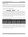


![2008 [DAMN SMALL NAS]](http://vs1.manualzilla.com/store/data/005757702_2-ad0d2f1082977ee9ed587e807bbc0127-150x150.png)