1
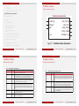
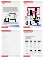
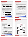
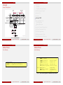
Introduction
1
Introduction
PicoBlaze
PicoBlaze Functional Blocks
2
PicoBlaze Interface Signals
3
Instruction Set
4
Interrupts
5
Scratchpad RAM
c Dr inż. Ignacy Pardyka
6
UNIWERSYTET
JANA KOCHANOWSKIEGO
w Kielcach1
Input and Output Ports
Input Operations
Output Operations
7
Instruction Storage Configurations
8
PicoBlaze Development Tools
9
PicoBlaze Programming
10
PicoBlaze Instruction Codes
11
Related Materials and References
PROGRAMOWANIE STRUKTUR CYFROWYCH
PicoBlaze
XILINX 8-bit Embedded Microcontroller
User Guide: UG129
Rok akad. 2011/2012
1
Instytut Fizyki, Zak-ad Informatyki, e-mail: [email protected]
J
c Dr inż. Ignacy Pardyka (Inf ∈ UK
)
programowanie struktur cyfrowych
Introduction
Rok akad. 2011/2012
1 / 96
J
c Dr inż. Ignacy Pardyka (Inf ∈ UK
)
programowanie struktur cyfrowych
PicoBlaze
Introduction
PicoBlaze Structure
UG129 (v2.0) January 28, 2010
1Kx18
Instruction
PROM
31x10
CALL/RETURN
Stack
PicoBlaze Block Diagram
PicoBlaze User Guide
Program Counter
(PC)
PicoBlaze
Rok akad. 2011/2012
2 / 96
PicoBlaze Functional Blocks
PORT_ID
64-Byte
Scratchpad RAM
OUT_PORT
Flags
Instruction
Decoder
Constants
INTERRUPT
IE
16 Byte-Wide Registers
Enable
s0
s4
s8
sC
IN_PORT
s1
s5
s9
sD
s2
s6
sA
sE
s3
s7
sB
sF
Operand 1
Z
Zero
C
Carry
ALU
Operand 2
UG129_c1_01_051204
Figure 1-1:
J
c Dr inż. Ignacy Pardyka (Inf ∈ UK
)
programowanie struktur cyfrowych
Rok akad. 2011/2012
3 / 96
J
c Dr inż. Ignacy Pardyka (Inf ∈ UK
)
PicoBlaze Embedded Microcontroller Block Diagram
programowanie struktur cyfrowych
Rok akad. 2011/2012
4 / 96
PicoBlaze Interface Signals
1
PicoBlaze Interface Signals
Introduction
PicoBlaze
PicoBlaze Functional Blocks
2
PicoBlaze Interface Signals
3
Instruction Set
4
Interrupts
5
Scratchpad RAM
6
Input and Output Ports
Input Operations
Output Operations
PicoBlaze Interface
PicoBlaze Interface Connections
PicoBlaze Microcontroller
IN_PORT[7:0]
INTERRUPT
PORT_ID[7:0]
RESET
READ_STROBE
WRITE_STROBE
7
Instruction Storage Configurations
8
PicoBlaze Development Tools
9
PicoBlaze Programming
10
PicoBlaze Instruction Codes
11
Related Materials and References
J
c Dr inż. Ignacy Pardyka (Inf ∈ UK
)
OUT_PORT[7:0]
INTERRUPT_ACK
CLK
UG129_c2_01_052004
Figure 2-1:
programowanie struktur cyfrowych
Rok akad. 2011/2012
5 / 96
J
c Dr inż. Ignacy Pardyka (Inf ∈ UK
)
PicoBlaze Interface Signals
PicoBlaze Interface Connections
programowanie struktur cyfrowych
6 / 96
PicoBlaze Interface Signals
PicoBlaze Interface
PicoBlaze Interface
PicoBlaze Interface Signals
PicoBlaze Interface Signals cont’d
Table 2-1:
Rok akad. 2011/2012
PicoBlaze Interface Signal Descriptions
Signal
IN_PORT[7:0]
Direction
Description
Input
Input Data Port: Present valid input data on this port during an INPUT instruction.
The data is captured on the rising edge of CLK.
INTERRUPT
Input
Interrupt Input: If the INTERRUPT_ENABLE flag is set by the application code,
generate an INTERRUPT Event by asserting this input High for at least two CLK
cycles. If the INTERRUPT_ENABLE flag is cleared, this input is ignored.
RESET
Input
Reset Input: To reset the PicoBlaze microcontroller and to generate a RESET Event,
assert this input High for at least one CLK cycle. A Reset Event is automatically
generated immediately following FPGA configuration.
CLK
Input
Clock Input: The frequency may range from DC to the maximum operating
frequency reported by the Xilinx ISE® development software. All PicoBlaze
synchronous elements are clocked from the rising clock edge. There are no clock
duty-cycle requirements beyond the minimum pulse width requirements of the
FPGA.
OUT_PORT[7:0]
Output
Output Data Port: Output data appears on this port for two CLK cycles during an
OUTPUT instruction. Capture output data within the FPGA at the rising CLK edge
when WRITE_STROBE is High.
PORT_ID[7:0]
Output
Port Address: The I/O port address appears on this port for two CLK cycles during
an INPUT or OUTPUT instruction.
J
c Dr inż. Ignacy Pardyka (Inf ∈ UK
)
programowanie struktur cyfrowych
Rok akad. 2011/2012
Table 2-1:
PicoBlaze Interface Signal Descriptions (Cont’d)
Signal
7 / 96
Direction
Description
READ_STROBE
Output
Read Strobe: When asserted High, this signal indicates that input data on the
IN_PORT[7:0] port was captured to the specified data register during an INPUT
instruction. This signal is asserted on the second CLK cycle of the two-cycle INPUT
instruction. This signal is typically used to acknowledge read operations from
FIFOs.
WRITE_STROBE
Output
Write Strobe: When asserted High, this signal validates the output data on the
OUT_PORT[7:0] port during an OUTPUT instruction. This signal is asserted on the
second CLK cycle of the two-cycle OUTPUT instruction. Capture output data
within the FPGA on the rising CLK edge when WRITE_STROBE is High.
INTERRUPT_ACK
Output
Interrupt Acknowledge: When asserted High, this signal acknowledges that an
INTERRUPT Event occurred. This signal is asserted during the second CLK cycle
of the two-cycle INTERRUPT Event. This signal is optionally used to clear the
source of the INTERRUPT input.
J
c Dr inż. Ignacy Pardyka (Inf ∈ UK
)
programowanie struktur cyfrowych
Rok akad. 2011/2012
8 / 96
PicoBlaze Interface Signals
PicoBlaze Interface Signals
PicoBlaze
PicoBlaze
KCPSM3
KCPSM3 Architecture
KCPSM3 is a very simple 8-bit microcontroller primarily for the Spartan-3 devices but also suitable for use in Virtex-II and VirtexIIPRO devices. Although it could be used for processing of data, it is most likely to be employed in applications requiring a
complex, but non-time critical state machine. Hence it has the name of ‘(K)constant Coded Programmable State Machine’.
16 Registers
8-bit
This revised version of popular KCPSM macro has still been developed with one dominant factor being held above all others Size! The result is a microcontroller which occupies just 96 Spartan-3 Slices which is just 5% of the XC3S200 device and less
than 0.3% of the XC3S5000 device. Together with this small amount of logic, a single block RAM is used to form a ROM store
for a program of up to 1024 instructions. Even with such size constraints, the performance is respectable at approximately 43 to
66 MIPS depending on device type and speed grade.
KCPSM3
IN_PORT[7:0]
Interface to logic
IN_PORT[7:0]
OUT_PORT[7:0]
INTERRUPT
pp
s7
s6
s5
s4
s3
s2
s1
s0
READ_STROBE
CLK
Port
Address
Control
Arithmetic
Logical
Shift
Rotate
kk
8 bit data path
INTERRUPT_ACK
PARITY
Scratch Pad
Memory
64-Bytes
18 bit instruction word
ZERO &
CARRY
flags
ss
8 bit port address
INSTRUCTION[17:0]
INSTRUCTION[17:0]
ADDRESS[9:0]
10 bit program address
ADDRESS[9:0]
INTERRUPT
Constants
INTERRUPT_ACK
INSTRUCTION[17:0]
One of the most exciting features of the KCPSM3 is that it is totally embedded into the device and requires no external support.
The very fact that ANY logic can be connected to the module inside the Spartan-3 or Virtex-II device means that any additional
features can be added to provide ultimate flexibility. It is not so much what is inside the KCPSM3 module that makes it useful,
but the environment in which it lives.
J
c Dr inż. Ignacy Pardyka (Inf ∈ UK
)
programowanie struktur cyfrowych
Rok akad. 2011/2012
1024 words
RESET
CLK
9 / 96
J
c Dr inż. Ignacy Pardyka (Inf ∈ UK
)
Instruction Set
1
PicoBlaze Interface Signals
3
Instruction Set
4
Interrupts
5
Scratchpad RAM
6
Input and Output Ports
Input Operations
Output Operations
Instruction Storage Configurations
8
PicoBlaze Development Tools
9
PicoBlaze Programming
10
PicoBlaze Instruction Codes
11
Related Materials and References
J
c Dr inż. Ignacy Pardyka (Inf ∈ UK
)
programowanie struktur cyfrowych
Program
Counter
ADDRESS[9:0]
Program
Counter
Stack
aaa / pp / ss / kk
programowanie struktur cyfrowych
Rok akad. 2011/2012
10 / 96
PicoBlaze Instruction Set
Instructions
‘X’ and ‘Y’ refer to the definition of the storage registers ‘s’ in the range 0 to F.
‘kk’ represents a constant value in the range 00 to FF.
‘aaa’ represents an address in the range 000 to 3FF.
‘pp’ represents a port address in the range 00 to FF.
‘ss’ represents an internal storage address in the range 00 to 3F.
Program Control Group
7
Program
Flow
Control
Instruction Set
Introduction
PicoBlaze
PicoBlaze Functional Blocks
2
aaa
Operational
control &
Instruction
decoding
Interrupt
Shadow Flags
Interrupt
Control
CLK
Program
ROM/RAM
READ_STROBE
WRITE_STROBE
OUT_PORT[7:0]
Interface to logic
WRITE_STROBE
PORT_ID[ 7:0]
ALU
PORT_ID[7:0]
RESET
Block Memory
(Program)
sF
sE
sD
sC
sB
sA
s9
s8
aaa
Z,aaa
NZ,aaa
C,aaa
NC,aaa
ADD sX,kk
ADDCY sX,kk
SUB sX,kk
SUBCY sX,kk
COMPARE sX,kk
CALL
CALL
CALL
CALL
CALL
aaa
Z,aaa
NZ,aaa
C,aaa
NC,aaa
ADD sX,sY
ADDCY sX,sY
SUB sX,sY
SUBCY sX,sY
COMPARE sX,sY
RETURN
RETURN
RETURN
RETURN
RETURN
Z
NZ
C
NC
Note that call and return supports
up to a stack depth of 31.
Rok akad. 2011/2012
11 / 96
Arithmetic Group
JUMP
JUMP
JUMP
JUMP
JUMP
J
c Dr inż. Ignacy Pardyka (Inf ∈ UK
)
Interrupt Group
RETURNI ENABLE
RETURNI DISABLE
ENABLE INTERRUPT
DISABLE INTERRUPT
Logical Group
Shift and Rotate Group
LOAD sX,kk
AND sX,kk
OR sX,kk
XOR sX,kk
TEST sX,kk
SR0 sX
SR1 sX
SRX sX
SRA sX
RR sX
LOAD sX,sY
AND sX,sY
OR sX,sY
XOR sX,sY
TEST sX,sY
SL0 sX
SL1 sX
SLX sX
SLA sX
RL sX
Storage Group
STORE
STORE
FETCH
FETCH
programowanie struktur cyfrowych
sX,ss
sX,(sY)
sX,ss
sX,(sY)
Input/Output Group
INPUT sX,pp
INPUT sX,(sY)
OUTPUT sX,pp
OUTPUT sX,(sY)
Rok akad. 2011/2012
12 / 96
Instruction Set
Instruction Set
PicoBlaze Instruction Set
PicoBlaze Instruction Set
JUMP
CALL
The CALL instruction is similar in operation to the JUMP instruction in that it will modify the normal program execution sequence by
specifying a new address. The CALL instruction may also be conditional. In addition to supplying a new address, the CALL
instruction also causes the current program counter (PC) value to be pushed onto the program counter stack. The CALL instruction
has no effect on the status of the flags.
Under normal conditions, the program counter (PC) increments to point to the next instruction. The address space is fixed to
1024 locations (000 to 3FF hex) and therefore the program counter is 10 bits wide. It is worth noting that the top of memory is
3FF hex and will increment to 000.
PC
PC
+1
Unconditional or
condition valid
The JUMP instruction may be used to modify this sequence by specifying a new address. However, the JUMP instruction may be
conditional. A conditional JUMP will only be performed if a test performed on either the ZERO flag or CARRY flag is valid. The
JUMP instruction has no effect on the status of the flags.
Condition
not valid
JUMP
JUMP
JUMP
JUMP
JUMP
14
13
0
1
0
Bit 12
12
11
10
9
8
7
6
5
4
3
2
1
0
a
a
a
a
a
a
a
a
a
a
0 - UNCONDITIONAL
1 - CONDITIONAL
J
c Dr inż. Ignacy Pardyka (Inf ∈ UK
)
0
0
1
1
0
1
0
1
programowanie struktur cyfrowych
Each CALL instruction must specify the 10-bit address as a 3 digit hexadecimal value. The assembler supports labels to simplify
this process.
Bit 11 Bit 10
Condition
17
if Zero
if NOT Zero
if Carry
if NOT Carry
Rok akad. 2011/2012
16
15
14
13
1 1
0
0
0
Bit 12
13 / 96
12
11
10
9
8
7
6
5
4
3
2
1
0
a
a
a
a
a
a
a
a
a
a
J
c Dr inż. Ignacy Pardyka (Inf ∈ UK
)
PicoBlaze Instruction Set
RETURNI
Stack
+1
PC
Stack
RETURN
RETURN
RETURN
RETURN
RETURN
+1
Unconditional or
condition valid
13
0
1
Bit 12
12
11
10
9
8
7
6
5
4
3
2
1
0
0
0
0
0
0
0
0
0
0
0
0 - UNCONDITIONAL
1 - CONDITIONAL
J
c Dr inż. Ignacy Pardyka (Inf ∈ UK
)
programowanie struktur cyfrowych
Preserved
CARRY
ZERO
Preserved
ZERO
INTERRUPT
ENABLED
Z
NZ
C
NC
Bit 11
Bit 10
0
0
1
1
0
1
0
1
ENABLE
DISABLE
14 / 96
‘1’
‘0’
It is the responsibility of the programmer to ensure that a RETURNI is only performed in response to an interrupt. Each RETURNI
must specify if further interrupt is to be enabled or disabled.
RETURNI ENABLE
14
CARRY
PC
It is the responsibility of the programmer to ensure that a RETURN is only performed in response to a previous CALL instruction
such that the program counter stack contains a valid address. The cyclic implementation of the stack will continue to provide
values for RETURN instructions which can not be defined.
1
Rok akad. 2011/2012
The RETURNI instruction is a special variation of the RETURN instruction which should be used to conclude an interrupt service
routine. The RETURNI is unconditional and therefore will always load the program counter (PC) with the last address on the
program counter stack (the address is not incremented in this case since the instruction at the address stored will need to be
executed). The RETURNI instruction restores the flags to the condition they were in at the point of interrupt. The RETURNI also
determines the future ability of interrupts using ENABLE and DISABLE as an operand.
The RETURN instruction is the complement to the CALL instruction. The RETURN instruction may also be conditional. In this case
the new program counter (PC) value will be formed internally by incrementing the last value on the program address stack. This
ensures that the program will execute the instruction following the CALL instruction which resulted in the subroutine. The RETURN
instruction has no effect on the status of the flags.
Condition
PC
not valid
15
if Zero
if NOT Zero
if Carry
if NOT Carry
Instruction Set
RETURN
16
0
1
0
1
programowanie struktur cyfrowych
PicoBlaze Instruction Set
1 0
0
0
1
1
0 - UNCONDITIONAL
1 - CONDITIONAL
Instruction Set
17
aaa
Z,aaa
NZ,aaa
C,aaa
NC,aaa
The program counter stack supports a depth of 31 address values. This enables nested ‘CALL’ sequences to a depth of 31 levels
to be performed. However, the stack will also be used during an interrupt operation and hence at least one of these levels should
be reserved when interrupts are enabled. The stack is implemented as a separate cyclic buffer. When the stack becomes full, it
simply overwrites the oldest value. Hence it is not necessary to reset the stack pointer when performing a software reset. This also
explains why there are no instructions to control the stack and why no other memory needs to be reserved or provided for the
stack.
aaa
Z,aaa
NZ,aaa
C,aaa
NC,aaa
Each JUMP instruction must specify the 10-bit address as a 3 digit hexadecimal value. The assembler supports labels to simplify
this process.
Bit 11 Bit 10
Condition
15
CALL
CALL
CALL
CALL
CALL
New Address
a a a a a a a a a a
Unconditional or
condition valid
Unconditional or
condition valid
16
+1
+1
New Address
a a a a a a a a a a
1 1
PC
PC
PC
PC
17
Condition
not valid
Stack
Normal Instruction
17
16
15
14
13
1
1
1
0
0
17
16
15
14
13
1
1
1
0
0
12
11
10
9
8
7
6
5
4
3
2
1
0
0 0
0
0
0
0
0
0
0
0
0
0
1
Condition
if Zero
if NOT Zero
if Carry
if NOT Carry
Rok akad. 2011/2012
RETURNI DISABLE
15 / 96
J
c Dr inż. Ignacy Pardyka (Inf ∈ UK
)
12
11
10
9
8
7
6
5
4
3
2
1
0
0 0
0
0
0
0
0
0
0
0
0
0
0
programowanie struktur cyfrowych
Rok akad. 2011/2012
16 / 96
Instruction Set
Instruction Set
PicoBlaze Instruction Set
PicoBlaze Instruction Set
ENABLE/DISABLE INTERRUPT
LOAD
The LOAD instruction provides a method for specifying the contents of any register. The new value can be a constant, or the
contents of any other register. The LOAD instruction has no effect on the status of the flags.
These instructions are used to set and reset the INT_ENABLE flag. Before using ENABLE INTERRUPT a suitable interrupt
routine must be associated with the interrupt address vector (located at address 3FF). Interrupts should never be enabled whilst
performing an interrupt service routine.
sX
Constant
sX
sY
k k k k k k k k
ENABLE
‘1’
INT_ENABLE
‘0’
DISABLE
Since the LOAD instruction does not effect the flags it may be used to reorder and assign register contents at any stage of the
program execution. The ability to assign a constant with no impact to the program size or performance means that the load
instruction is the most obvious way to assign a value or clear a register.
The first operand of a LOAD instruction must specify the register to be loaded as register ‘s’ followed by a hexadecimal digit. The
second operand must then specify a second register value in a similar way or specify an 8-bit constant using 2 hexadecimal digits.
The assembler supports register naming and constant labels to simplify the process.
Interrupts are masked when the INT_ENABLE flag is low. This is the default state of the flag following device configuration or a
KCPSM3 reset. The INT_ENABLE is also reset during an active interrupt.
ENABLE INTERRUPT
DISABLE INTERRUPT
17
16
15
14
13
1
1
1
1
0
17
16
15
14
13
1
1
1
1
0
12
11
10
9
8
7
6
5
4
3
2
1
0
0 0
0
0
0
0
0
0
0
0
0
0
1
11
10
9
8
7
6
5
4
3
2
1
0
0 0
0
0
0
0
0
0
0
0
0
0
0
12
LOAD sX,kk
17
16
15
14
0
0
0
0
13
12
11
10
9
8
7
6
5
4
3
2
1
0
0 0
x
x
x
x
k
k
k
k
k
k
k
k
17
16
15
14
13
12
11
10
9
8
7
6
5
0
0
0
0
0
4
3
2
1
0
1
x
x
x
x
y
y
y
y
0
0
0
0
sX
LOAD sX,sY
Constant
sY
sX
J
c Dr inż. Ignacy Pardyka (Inf ∈ UK
)
programowanie struktur cyfrowych
Rok akad. 2011/2012
17 / 96
J
c Dr inż. Ignacy Pardyka (Inf ∈ UK
)
programowanie struktur cyfrowych
Instruction Set
PicoBlaze Instruction Set
AND
OR
The OR instruction performs a bit-wise logical ‘OR’ operation between two operands. For example 00001111 OR 00110011 will
produce the result 00111111. The first operand is any register, and it is this register which will be assigned the result of the
operation. A second operand may also be any register or an 8-bit constant value. Flags will be effected by this operation. OR
provides a way to force any bits of the specified register to be set which can be useful in forming control signals.
The AND instruction performs a bit-wise logical ‘AND’ operation between two operands. For example 00001111 AND 00110011
will produce the result 00000011. The first operand is any register, and it is this register which will be assigned the result of the
operation. A second operand may also be any register or an 8-bit constant value. Flags will be effected by this operation. The AND
operation is useful for resetting bits of a register and performing tests on the contents (see also TEST instruction). The status of
the ZERO flag will then control the flow of the program.
sX
sX
Constant
AND
sX
sX
Constant
OR
sX
sY
sX
sY
OR
AND
0
ZERO
17
16
15
14
0
0
1
0
13
12
11
10
9
8
7
6
5
4
3
2
1
0
1 0
x
x
x
x
k
k
k
k
k
k
k
k
17
16
15
14
13
12
11
10
9
8
7
6
5
4
3
2
1
0
0
0
1
0
1
1
x
x
x
x
y
y
y
y
0
0
0
0
sX
AND sX,sY
programowanie struktur cyfrowych
Set if all bits of result are zero.
Reset in all other cases.
?
OR sX,kk
17
16
15
14
0
0
1
1
13
12
11
10
9
8
7
6
5
4
3
2
1
0
0 0
x
x
x
x
k
k
k
k
k
k
k
k
17
16
15
14
13
12
11
10
9
8
7
6
5
0
0
1
1
0
4
3
2
1
0
1
x
x
x
x
y
y
y
y
0
0
0
0
sX
Constant
sX
J
c Dr inż. Ignacy Pardyka (Inf ∈ UK
)
ZERO
Each OR instruction must specify the first operand register as ‘s’ followed by a hexadecimal digit. This register will also form the
destination for the result. The second operand must then specify a second register value in a similar way or specify an 8-bit
constant using 2 hexadecimal digits. The assembler supports register naming and constant labels to simplify the process.
Each AND instruction must specify the first operand register as ‘s’ followed by a hexadecimal digit. This register will also form the
destination for the result. The second operand must then specify a second register value in a similar way or specify an 8-bit
constant using 2 hexadecimal digits. The assembler supports register naming and constant labels to simplify the process.
AND sX,kk
0
CARRY
Set if all bits of result are zero.
Reset in all other cases.
?
k k k k k k k k
k k k k k k k k
sX
CARRY
18 / 96
Instruction Set
PicoBlaze Instruction Set
sX
Rok akad. 2011/2012
OR sX,sY
Constant
sX
sY
Rok akad. 2011/2012
19 / 96
J
c Dr inż. Ignacy Pardyka (Inf ∈ UK
)
programowanie struktur cyfrowych
sY
Rok akad. 2011/2012
20 / 96
Instruction Set
Instruction Set
PicoBlaze Instruction Set
PicoBlaze Instruction Set
XOR
TEST
The TEST instruction performs a bit-wise logical ‘AND’ operation between two operands. Unlike the ‘AND’ instruction, the result of
the operation is discarded and only the flags are affected. The ZERO flag is set if all bits of the temporary result are low. The
CARRY flag is used to indicate the ODD PARITY of the temporary result. Parity checks typically involve a test of all bits, i.e. if the
contents of ‘s5’ = 3D (00111101), the execution of TEST s5,FF will set the CARRY flag indicating ODD parity. Bit testing is typically
used to isolate a single bit. For example TEST s5,04 will test bit2 of the ‘s5’ register which would set the CARRY flag if the bit is
high (reset if the bit is low) and set the ZERO flag if the bit is low (reset if the bit is high).
The XOR instruction performs a bit-wise logical ‘XOR’ operation between two operands. For example 00001111 XOR 00110011
will produce the result 00111100. The first operand is any register, and it is this register which will be assigned the result of the
operation. A second operand may also be any register or an 8-bit constant value. Flags will be effected by this operation. The XOR
operation is useful for inverting bits contained in a register which is useful in forming control signals.
sX
sX
Constant
XOR
Temporary
k k k k k k k k
sX
Constant
AND
sX
sX
k k k k k k k k
sY
XOR
sX
Temporary
sY
AND
0
CARRY
Set if all bits of result are zero.
Reset in all other cases.
?
ZERO
CARRY
Each XOR instruction must specify the first operand register as ‘s’ followed by a hexadecimal digit. This register will also form the
destination for the result. The second operand must then specify a second register value in a similar way or specify an 8-bit
constant using 2 hexadecimal digits. The assembler supports register naming and constant labels to simplify the process.
XOR sX,kk
17
16
15
14
0
0
1
1
13
12
11
10
9
8
7
6
5
4
3
2
1
0
1 0
x
x
x
x
k
k
k
k
k
k
k
k
sX
XOR sX,sY
Each TEST instruction must specify the first operand register as ‘s’ followed by a hexadecimal digit. The second operand must
then specify a second register value in a similar way or specify an 8-bit constant using 2 hexadecimal digits. The assembler
supports register naming and constant labels to simplify the process.
TEST sX,kk
17
16
15
14
0
1
0
0
13
12
11
10
9
8
7
6
5
4
3
2
1
0
1 0
x
x
x
x
k
k
k
k
k
k
k
k
17
16
15
14
13
12
11
10
9
8
7
6
5
0
1
0
0
1
4
3
2
1
0
1
x
x
x
x
y
y
y
y
0
0
0
0
sX
16
15
14
13
12
11
10
9
8
7
6
5
4
3
2
1
0
0
0
1
1
1
1
x
x
x
x
y
y
y
y
0
0
0
0
TEST sX,sY
sY
sX
Rok akad. 2011/2012
21 / 96
J
c Dr inż. Ignacy Pardyka (Inf ∈ UK
)
sY
programowanie struktur cyfrowych
Instruction Set
PicoBlaze Instruction Set
ADD
ADDCY
The ADD instruction performs an 8-bit addition of two operands. The first operand is any register, and it is this register which will be
assigned the result of the operation. A second operand may also be any register or an 8-bit constant value. Flags will be effected
by this operation. Note that this instruction does not use the CARRY as an input, and hence there is no need to condition the flags
before use. The ability to specify any constant is useful in forming control sequences and counters.
sX
sX
sX
Constant
+
k k k k k k k k
sX
sY
sX
Set if result of addition exceeds FF.
Reset in all other cases.
sY
Set if all bits of result are zero.
Reset in all other cases.
CARRY
Each ADD instruction must specify the first operand register as ‘s’ followed by a hexadecimal digit. This register will also form the
destination for the result. The second operand must then specify a second register value in a similar way or specify an 8-bit
constant using 2 hexadecimal digits. The assembler supports register naming and constant labels to simplify the process.
ADD sX,kk
17
16
15
14
0
1
1
0
13
12
11
10
9
8
7
6
5
4
3
2
1
0
0 0
x
x
x
x
k
k
k
k
k
k
k
k
17
16
15
14
13
12
11
10
9
8
7
6
5
4
3
2
1
0
0
1
1
0
0
1
x
x
x
x
y
y
y
y
0
0
0
0
sX
ADD sX,sY
Set if result of addition exceeds FF.
Reset in all other cases.
CARRY
programowanie struktur cyfrowych
Set if all bits of result are zero.
Reset in all other cases.
?
ZERO
Each ADDCY instruction must specify the first operand register as ‘s’ followed by a hexadecimal digit. This register will also
form the destination for the result. The second operand must then specify a second register value in a similar way or specify an
8-bit constant using 2 hexadecimal digits. The assembler supports register naming and constant labels to simplify the process.
ADDCY sX,kk
17
16
15
14
0
1
1
0
13
12
11
10
9
8
7
6
5
4
3
2
1
0
1 0
x
x
x
x
k
k
k
k
k
k
k
k
17
16
15
14
13
12
11
10
9
8
7
6
5
0
1
1
0
1
4
3
2
1
0
1
x
x
x
x
y
y
y
y
0
0
0
0
sX
Constant
sX
J
c Dr inż. Ignacy Pardyka (Inf ∈ UK
)
?
ADDCY sX,sY
Constant
sX
sY
Rok akad. 2011/2012
+
+
+
?
ZERO
CARRY
k k k k k k k k
sX
+
?
22 / 96
The ADDCY instruction performs an addition of two 8-bit operands together with the contents of the CARRY flag. The first operand
is any register, and it is this register which will be assigned the result of the operation. A second operand may also be any register
or an 8-bit constant value. Flags will be effected by this operation. The ADDCY operation can be used in the formation of adder
and counter processes exceeding 8 bits.
Constant
+
CARRY
Rok akad. 2011/2012
Instruction Set
PicoBlaze Instruction Set
sX
Constant
sX
programowanie struktur cyfrowych
sX
Set if all bits of temporary result are zero.
Reset in all other cases.
?
ZERO
Constant
17
J
c Dr inż. Ignacy Pardyka (Inf ∈ UK
)
?
Set if there are an odd number of bits
set to ‘1’ in the temporary result.
23 / 96
J
c Dr inż. Ignacy Pardyka (Inf ∈ UK
)
programowanie struktur cyfrowych
sY
Rok akad. 2011/2012
24 / 96
Instruction Set
Instruction Set
PicoBlaze Instruction Set
PicoBlaze Instruction Set
SUB
SUBCY
The SUB instruction performs an 8-bit subtraction of two operands. The first operand is any register, and it is this register which will
be assigned the result of the operation. The second operand may also be any register or an 8-bit constant value. Flags will be
effected by this operation. Note that this instruction does not use the CARRY as an input, and hence there is no need to condition
the flags before use. The CARRY flag indicates when an underflow has occurred. For example, if ‘s05’ contains 27 hex and the
instruction SUB s05,35 is performed, then the stored result will be F2 hex and the CARRY flag will be set.
sX
sX
sX
Constant
-
sX
The SUBCY instruction performs an 8-bit subtraction of two operands together with the contents of the CARRY flag. The first
operand is any register, and it is this register which will be assigned the result of the operation. The second operand may also be
any register or an 8-bit constant value. Flags will be effected by this operation. The SUBCY operation can be used in the formation
of subtract and down counter processes exceeding 8 bits.
sX
Constant
-
k k k k k k k k
sX
sX
sY
sX
sY
Set if result is negative.
Reset in all other cases.
?
Set if all bits of result are zero.
Reset in all other cases.
?
ZERO
CARRY
Each SUB instruction must specify the first operand register as ‘s’ followed by a hexadecimal digit. This register will also form the
destination for the result. The second operand must then specify a second register value in a similar way or specify an 8-bit
constant using 2 hexadecimal digits. The assembler supports register naming and constant labels to simplify the process.
SUB sX,kk
17
16
15
14
0
1
1
1
13
12
11
10
9
8
7
6
5
4
3
2
1
0
0 0
x
x
x
x
k
k
k
k
k
k
k
k
17
16
15
14
13
12
11
10
9
8
7
6
5
4
3
2
1
0
0
1
1
1
0
1
x
x
x
x
y
y
y
y
0
0
0
0
sX
SUB sX,sY
Set if result is negative.
Reset in all other cases.
Each SUBCY instruction must specify the first operand register as ‘s’ followed by a hexadecimal digit. This register will also
form the destination for the result. The second operand must then specify a second register value in a similar way or specify an
8-bit constant using 2 hexadecimal digits. The assembler supports register naming and constant labels to simplify the process.
SUBCY sX,kk
17
16
15
14
0
1
1
1
13
12
11
10
9
8
7
6
5
4
3
2
1
0
1 0
x
x
x
x
k
k
k
k
k
k
k
k
17
16
15
14
13
12
11
10
9
8
7
6
5
0
1
1
1
1
4
3
2
1
0
1
x
x
x
x
y
y
y
y
0
0
0
0
sX
SUBCY sX,sY
sY
Rok akad. 2011/2012
25 / 96
J
c Dr inż. Ignacy Pardyka (Inf ∈ UK
)
Instruction Set
PicoBlaze Instruction Set
SR0, SR1, SRX, SRA, RR
sX
sX
Set if ‘sY’ or ‘kk’ is greater than ‘sX’.
Reset in all other cases.
COMPARE sX,kk
0
1
0
1
13
sX
Set if operands are equal.
Reset in all other cases.
?
ZERO
12
11
10
9
8
7
6
5
4
3
2
1
0
0 0
x
x
x
x
k
k
k
k
k
k
k
k
sX
COMPARE sX,sY
SRA sX
RR sX
Set if all bits of result are zero.
Reset in all other cases.
ZERO
?
ZERO
0
ZERO
?
Set if all bits of result are zero.
Reset in all other cases.
ZERO
?
Set if all bits of result are zero.
Reset in all other cases.
ZERO
?
Set if all bits of result are zero.
Reset in all other cases.
CARRY
CARRY
16
15
14
13
12
11
10
9
8
7
6
5
4
3
2
1
0
0
1
0
1
0
1
x
x
x
x
y
y
y
y
0
0
0
0
sX
programowanie struktur cyfrowych
sY
Rok akad. 2011/2012
sX
sX
CARRY
CARRY
Each instruction must specify the register as ‘s’ followed by a hexadecimal digit. The assembler supports register naming to
simplify the process.
Bit 2 Bit 1 Bit 0
Instruction
17 16 15 14 13 12 11 10
9
8
7
6
5
4
3
2
1
0
1
1
0
SR0 sX
1
1
1
SR1 sX
1 0 0 0 0 0 x x x x 0 0 0 0 1
0
1
0
SRX sX
0
0
0
SRA sX
sX
1
0
0
RR sX
Constant
17
J
c Dr inż. Ignacy Pardyka (Inf ∈ UK
)
‘1’
CARRY
SRX sX
Each COMPARE instruction must specify the first operand register as ‘s’ followed by a hexadecimal digit. The second operand
must then specify a second register value in a similar way or specify an 8-bit constant using 2 hexadecimal digits. The assembler
supports register naming and constant labels to simplify the process.
14
SR1 sX
sY
-
15
‘0’
k k k k k k k k
sX
16
SR0 sX
sX
Constant
-
17
26 / 96
The shift and rotate right group all modify the contents of a single register. All instructions in the group have an effect on the flags.
The COMPARE instruction performs an 8-bit subtraction of two operands Unlike the ‘SUB’ instruction, the result of the operation is
discarded and only the flags are affected. The ZERO flag is set when all the bits of the temporary result are low and indicates that
both input operands were identical. The CARRY flag indicates when an underflow has occurred and indicates that the second
operand was larger than the first. For example, if ‘s05’ contains 27 hex and the instruction COMPARE s05,35 is performed, then
the CARRY flag will be set (35>27) and the ZERO flag will be reset (35≠27).
?
Rok akad. 2011/2012
Instruction Set
COMPARE
CARRY
sY
programowanie struktur cyfrowych
PicoBlaze Instruction Set
Temporary
Constant
sX
programowanie struktur cyfrowych
Temporary
CARRY
Set if all bits of result are zero.
Reset in all other cases.
?
ZERO
Constant
sX
J
c Dr inż. Ignacy Pardyka (Inf ∈ UK
)
?
-
-
CARRY
CARRY
k k k k k k k k
27 / 96
J
c Dr inż. Ignacy Pardyka (Inf ∈ UK
)
programowanie struktur cyfrowych
Rok akad. 2011/2012
28 / 96
Instruction Set
Instruction Set
PicoBlaze Instruction Set
PicoBlaze Instruction Set
SL0, SL1, SLX, SLA, RL
STORE
The shift and rotate left group all modify the contents of a single register. All instructions in the group have an effect on the flags.
CARRY
sX
CARRY
sX
SL0 sX
‘0’
ZERO
?
‘1’
ZERO
0
ZERO
?
Scratch pad
memory
SL1 sX
SLX sX
Scratch pad
memory
3F
sX
CARRY
The STORE instruction enables the contents of any register to be transferred to the 64-byte internal scratch pad memory. The
storage address (in the range 00 to 3F) can be defined by a constant value or indirectly as the contents of any other register. The
Flags are not affected by this operation.
Set if all bits of result are zero.
Reset in all other cases.
Set if all bits of result are zero.
Reset in all other cases.
3F
sX
address
sX
Constant
sY
address
0 0 s s s s s s
00
sX
CARRY
SLA sX
?
Set if all bits of result are zero.
Reset in all other cases.
ZERO
?
Set if all bits of result are zero.
Reset in all other cases.
sX
CARRY
RL sX
ZERO
Each STORE instruction must specify the source register as ‘s’ followed by a hexadecimal digit. It must then specify the storage
address using a register value in a similar way or specify a 6-bit constant storage address using 2 hexadecimal digits. The
assembler supports register naming and constant labels to simplify the process. Although the assembler will reject constants
greater than 3F, it is the responsibility of the programmer to ensure that the value of ‘sY’ is within the address range.
STORE sX,PP
Each instruction must specify the register as ‘s’ followed by a hexadecimal digit. The assembler supports register naming to
simplify the process.
Bit 2 Bit 1 Bit 0
Instruction
17 16 15 14 13 12 11 10
9
8
7
6
5
4
3
2
1
0
1
1
0
SL0 sX
1
1
SL1 sX
1
1 0 0 0 0 0 x x x x 0 0 0 0 0
0
0
SLX sX
1
0
0
0
SLA sX
sX
0
1
0
RL sX
J
c Dr inż. Ignacy Pardyka (Inf ∈ UK
)
programowanie struktur cyfrowych
Rok akad. 2011/2012
00
17
16
15
14
1
0
1
1
13
12
11
10
9
8
7
6
5
4
3
2
1
0
1 0
x
x
x
x
0
0
s
s
s
s
s
s
17
16
15
14
13
12
11
10
9
8
7
6
5
1
0
1
1
1
4
3
2
1
0
1
x
x
x
x
y
y
y
y
0
0
0
0
sX
STORE sX,(sY)
29 / 96
J
c Dr inż. Ignacy Pardyka (Inf ∈ UK
)
programowanie struktur cyfrowych
PicoBlaze Instruction Set
FETCH
OUTPUT
Scratch pad
memory
Port Value
Scratch pad
memory
3F
sY
address
Port Value
00
Each FETCH instruction must specify the destination register as ‘s’ followed by a hexadecimal digit. It must then specify the
storage address using a register value in a similar way or specify a 6-bit constant storage address using 2 hexadecimal digits.
The assembler supports register naming and constant labels to simplify the process. Although the assembler will reject
constants greater than 3F, it is the responsibility of the programmer to ensure that the value of ‘sY’ is within the address range.
16
15
14
0
0
0
1
13
17
16
15
14
13
12
11
10
9
8
7
6
5
4
3
2
1
0
1 0
x
x
x
x
0
0
s
s
s
s
s
s
12
11
10
9
8
7
6
5
4
3
2
1
0
0
0
0
1
1
1
x
x
x
x
y
y
y
y
0
0
0
0
sX
FETCH sX,(sY)
sX
programowanie struktur cyfrowych
Constant
PORT_ID Address
sY
Each OUTPUT instruction must specify the source register as ‘s’ followed by a hexadecimal digit. It must then specify the output
port address using a register value in a similar way or specify an 8-bit constant port identifier using 2 hexadecimal digits. The
assembler supports register naming and constant labels to simplify the process.
OUTPUT sX,PP
17
16
15
14
1
0
1
1
13
12
11
10
9
8
7
6
5
4
3
2
1
0
0 0
x
x
x
x
p
p
p
p
p
p
p
p
17
16
15
14
13
12
11
10
9
8
7
6
1
0
1
1
0
5
4
3
2
1
0
1
x
x
x
x
y
y
y
y
0
0
0
0
sX
Constant address
sX
J
c Dr inż. Ignacy Pardyka (Inf ∈ UK
)
PORT_ID Address
The user interface logic is required to decode the PORT_ID port address value and capture the data provided on the OUT_PORT.
The WRITE_STROBE is set during an output operation (see ‘READ and WRITE STROBES’), and should be used to clock enable
the capture register or write enable a RAM (see ‘Design of Output Ports’).
address
0 0 s s s s s s
00
sX
p p p p p p p p
3F
sX
17
30 / 96
The OUTPUT instruction enables the contents of any register to be transferred to logic external to KCPSM3. The port address (in
the range 00 to FF) can be defined by a constant value or indirectly as the contents of any other register. The Flags are not
affected by this operation.
The FETCH instruction enables data held in the 64-byte internal scratch pad memory to be transferred any of the internal
registers. The storage address (in the range 00 to 3F) can be defined by a constant value or indirectly as the contents of any
other register. The Flags are not affected by this operation.
FETCH sX,PP
Rok akad. 2011/2012
Instruction Set
PicoBlaze Instruction Set
Constant
sY
sX
Instruction Set
sX
Constant address
OUTPUT sX,(sY)
Constant PORT_ID
sX
sY
Rok akad. 2011/2012
31 / 96
J
c Dr inż. Ignacy Pardyka (Inf ∈ UK
)
programowanie struktur cyfrowych
sY
Rok akad. 2011/2012
32 / 96
Instruction Set
Instruction Set
PicoBlaze Instruction Set
PicoBlaze Instruction Set
INPUT
READ and WRITE STROBES
The INPUT instruction enables data values external to KCPSM3 to be transferred into any one of the internal registers. The port
address (in the range 00 to FF) can be defined by a constant value or indirectly as the contents of any other register. The Flags are
not affected by this operation.
sX
Port Value
PORT_ID Address
These pulses are used by external circuits to confirm input and output operations. In the waveforms below, it is assumed that the
content of register sE is 47, and the content of register sA is 42.
CLK
Constant
p p p p p p p p
sX
Port Value
PORT_ID Address
ADDRESS[9:0]
18A
INSTRUCTION[17:0]
sY
18C
18B
inst18A
INPUT s2,(sE)
PORT_ID[7:0]
47
INPUT sX,PP
15
14
0
0
0
1
13
12
11
10
0 0
x
x
9
8
7
6
5
4
3
2
1
0
x
x
p
p
p
p
p
p
p
p
sX
INPUT sX,(sY)
16
15
14
13
12
11
10
9
8
7
6
5
4
3
2
1
0
0
0
0
1
0
1
x
x
x
x
y
y
y
y
0
0
0
0
42
J
c Dr inż. Ignacy Pardyka (Inf ∈ UK
)
KCPSM3 captures data into s2
register on this clock edge.
programowanie struktur cyfrowych
Use WRITE_STROBE to clock
enable external circuit and
capture data on this clock edge
PORT_ID[7:0] is valid for 2 clock cycles providing additional time for external decoding logic and enabling the connection of
synchronous RAM. The WRITE_STROBE is provided on the second clock cycle to confirm an active write by KCPSM3. In most
cases, the READ_STROBE will not be utilised by the external decoding logic, but again occurs in the second cycle and indicates
the actual clock edge on which data is read into the specified register.
Note for timing critical designs, your timing specifications can allow 2 clock cycles for PORT_ID and data paths, and only the
strobes need to be constrained to a single clock cycle. Ideally, a pipeline register can be inserted where possible (see ‘Design of
Input Ports’, ‘Design of Output Ports’ and ‘Connecting Memory’).
sY
sX
65
READ_STROBE
Constant PORT_ID
17
18F
inst18E
WRITE_STROBE
Each INPUT instruction must specify the destination register as ‘s’ followed by a hexadecimal digit. It must then specify the input
port address using a register value in a similar way or specify an 8-bit constant port identifier using 2 hexadecimal digits. The
assembler supports register naming and constant labels to simplify the process.
16
18E
OUTPUT sA,65
OUT_PORT[7:0]
The user interface logic is required to decode the PORT_ID port address value and supply the correct data to the IN_PORT. The
READ_STROBE is set during an input operation (see ‘READ and WRITE STROBES’), but it is not always necessary for the
interface logic to decode this strobe. However, it can be useful for determining when data has been read, such as when reading a
FIFO buffer (see ‘Design of Input Ports’).
17
18D
inst18C
Rok akad. 2011/2012
33 / 96
J
c Dr inż. Ignacy Pardyka (Inf ∈ UK
)
Instruction Set
programowanie struktur cyfrowych
Rok akad. 2011/2012
34 / 96
Instruction Set
PicoBlaze
Moving Data
KCPSM3 RESET
Moving Data
KCPSM3 contains an internal reset control circuit to ensure the correct start up of KCPSM3 following device configuration or
global reset (GSR). This reset can also be activated within your design.
reset
The KCPSM3 reset is sampled synchronous to the clock and used to
form a controlled internal reset signal which is distributed locally as
required. A small ‘filter’ circuit (see right) ensures that the release of the
internal reset is clean and controlled.
FDS
FDS
Scratchpad RAM
internal_reset
Release of Reset after configuration.
CLK
STORE
GSR=1
FETCH
Registers
internal_reset
ADDRESS[9:0]
000
INSTRUCTION[17:0]
001
inst000
Application of user reset input
002
inst001
003
inst002
IN_PORT
004
OUT_PORT
LOAD sX, sY
INPUT
OUTPUT
inst003
INPUT sX, (sY)
OUTPUT sX, (sY)
LOAD sX, kk
The reset input can be tied to logic ‘0’ if not required and the ‘filter’ will still be used to
ensure correct power-up sequence.
CLK
RESET
Instruction
Store
internal_reset
ADDRESS[9:0]
INSTRUCTION[17:0]
123
124
inst123
000
inst124
inst000
001
PORT_ID
INPUT sX, kk
OUTPUT sX, kk
002
UG129_c3_05_060404
inst001
Figure 3-26:
J
c Dr inż. Ignacy Pardyka (Inf ∈ UK
)
programowanie struktur cyfrowych
Rok akad. 2011/2012
35 / 96
J
c Dr inż. Ignacy Pardyka (Inf ∈ UK
)
Data Movement Instructions
programowanie struktur cyfrowych
Rok akad. 2011/2012
36 / 96
Instruction Set
Interrupts
JUMP
1
Introduction
PicoBlaze
PicoBlaze Functional Blocks
2
PicoBlaze Interface Signals
3
Instruction Set
4
Interrupts
5
Scratchpad RAM
6
Input and Output Ports
Input Operations
Output Operations
7
Instruction Storage Configurations
8
PicoBlaze Development Tools
9
PicoBlaze Programming
10
PicoBlaze Instruction Codes
11
Related Materials and References
JUMP and CALL/RETURN
ADDRESS 000
main:
JUMP C, skip_over
If CARRY is set, load the PC with the
address of the label skip_over.
A
CALL my_subroutine
ADD s0, s1
skip_over:
3
1
Call my_subroutine. Save
the current PC to top of CALL/
RETURN stack. Load the PC with
the address of my_subroutine.
JUMP main
my_subroutine:
2
Return from my_subroutine.
Load the PC with the top of the CALL/
RETURN stack plus 1. Execute the
instruction immediately following
the associated CALL instruction.
RETURN
UG129_c3_06_051404
Figure 3-27:
Example JUMP and CALL/RETURN Procedures
J
c Dr inż. Ignacy Pardyka (Inf ∈ UK
)
programowanie struktur cyfrowych
Rok akad. 2011/2012
37 / 96
J
c Dr inż. Ignacy Pardyka (Inf ∈ UK
)
programowanie struktur cyfrowych
Interrupts
Rok akad. 2011/2012
38 / 96
Interrupts
Interrupts
Interrupts
Interrupt Logic
Interrupt Flow
ADDRESS 000
main:
Interrupt signal
INTERRUPT
input
asserted.
1
The interrupt input is not
recognized until the
INTERRUPT_ENABLE flag is set.
ENABLE INTERRUPT
INPUT s0, 00
INPUT s1, 01
ADD s0, s1
OUTPUT s0, 00
2
6
PicoBlaze Microcontroller
SET
D
CALL critical_timing
2
Q
JUMP main
INTERRUPT
In timing-critical functions or areas
where absolute predictability is
required, temporarily disable the
interrupt. Re-enable the interrupt
input when the time-critical function
is complete.
critical_timing: DISABLE INTERRUPT
RST
ENABLE INTERRUPT
RETURN
INTERRUPT_ACK
3
Always return from a sub-routine
call with the RETURN instruction.
isr: TEST s7, 02
The interrupt input is automatically
disabled.
5
4
Figure 4-1:
Use the RETURNI instruction to
return from an interrupt.
RETURNI ENABLE
UG129_c4_01_060404
Simple Interrupt Logic
3
ADDRESS 3FF
JUMP isr
The interrupt vector is always
located at the most-significant
memory location, where all the
address bits are ones. Jump to the
interrupt service routine.
UG129_c4_02_051404
Figure 4-2:
J
c Dr inż. Ignacy Pardyka (Inf ∈ UK
)
programowanie struktur cyfrowych
Rok akad. 2011/2012
39 / 96
J
c Dr inż. Ignacy Pardyka (Inf ∈ UK
)
Example Interrupt Flow
programowanie struktur cyfrowych
Rok akad. 2011/2012
40 / 96
Interrupts
Scratchpad RAM
Interrupts
1
Introduction
PicoBlaze
PicoBlaze Functional Blocks
2
PicoBlaze Interface Signals
3
Instruction Set
4
Interrupts
5
Scratchpad RAM
6
Input and Output Ports
Input Operations
Output Operations
7
Instruction Storage Configurations
8
PicoBlaze Development Tools
9
PicoBlaze Programming
10
PicoBlaze Instruction Codes
11
Related Materials and References
Interrupt Timing Diagram
Begin executing
interrupt service
routine
Interrupt
recognized
5 clock cycles
CLK
PREEMPTED
INSTRUCTION
INPUT s1,01
ADDRESS[9:0]
ADD s0,s1
Address of
ADD s0,s1
...
INTERRUPT
3
JUMP isr
3FF
4
TEST s7,02
isr
2
INTERRUPT_ACK
ADD s0,s1 instruction
pre-empted. PC saved to
stack. Flags preserved.
Interrupt disabled.
CALL/RETURN
Stack
Preserved
ZERO Flag
Call to interrupt
Jump to interrupt
service routine
vector, assert
INTERRUPT_ACK
ZERO
Flag
Preserved
CARRY Flag
CARRY
Flag
1
INTERRUPT_ENABLE
Figure 4-3:
J
c Dr inż. Ignacy Pardyka (Inf ∈ UK
)
0
UG129_c4_03_051404
Interrupt Timing Diagram
programowanie struktur cyfrowych
Rok akad. 2011/2012
41 / 96
J
c Dr inż. Ignacy Pardyka (Inf ∈ UK
)
Scratchpad RAM
programowanie struktur cyfrowych
Rok akad. 2011/2012
42 / 96
Scratchpad RAM
Address Modes
Address Modes
Direct Addressing
Indirect Addressing
NAMEREG s0, ram_data
NAMEREG s1, ram_address
CONSTANT ram_locations, 40
CONSTANT initial_value, 00
scratchpad_transfers:
STORE sX, 04 ; Write register sX to RAM location 04
FETCH sX, 04 ; Read RAM location 04 into register sX
Figure 5-1:
LOAD ram_data, initial_value
; load initial value
LOAD ram_address, ram_locations ; fill from top to bottom
Directly Addressing Scratchpad RAM Locations
ram_fill: SUB ram_address, 01
STORE ram_data, (ram_address)
JUMP NZ, ram_fill
Figure 5-2:
J
c Dr inż. Ignacy Pardyka (Inf ∈ UK
)
programowanie struktur cyfrowych
Rok akad. 2011/2012
; there are 64 locations
; initialize to zero
43 / 96
;
;
;
;
decrement address
initialize location
if not address 0, goto
ram_fill
Indirect Addressing Initializes All of RAM with a Simple Subroutine
J
c Dr inż. Ignacy Pardyka (Inf ∈ UK
)
programowanie struktur cyfrowych
Rok akad. 2011/2012
44 / 96
Scratchpad RAM
Scratchpad RAM
Scratchpad RAM
Stack Operations in Program
FETCH Operation
Stack in RAM
64-Byte Scratchpad RAM
DATA_IN[7:0]
FALSE
DATA_OUT[7:0]
NAMEREG sF, stack_ptr
Register sX
my_subroutine:
; preserve register s0
CALL push_s0
WRITE_ENABLE
[5:0]
Register sY or
Literal kk
; *** remainder of subroutine algorithm ***
ADDRESS[5:0]
[7]
[6]
; restore register s0
CALL pop_s0
RETURN
UG129_aC_11_051604
Figure C-5:
push_s0:
STORE s0, stack_ptr ; preserve register s0 onto “stack”
ADD stack_ptr, 01
; increment stack pointer
RETURN
FETCH Operation
Examples
FETCH sX, (sY) ; Read scratchpad RAM location specified by the
; contents of register sY into register sX
FETCH sX, kk
J
c Dr inż. Ignacy Pardyka (Inf ∈ UK
)
pop_s0:
SUB stack_ptr, 01
; decrement stack pointer
FETCH s0, stack_ptr ; restore register s0 from “stack”
RETURN
; Read scratchpad RAM location specified by the
; immediate constant kk into register sX
programowanie struktur cyfrowych
Rok akad. 2011/2012
Figure 5-4:
45 / 96
PicoBlaze Interface Signals
3
Instruction Set
4
Interrupts
5
Scratchpad RAM
6
Input and Output Ports
Input Operations
Output Operations
programowanie struktur cyfrowych
Rok akad. 2011/2012
46 / 96
Input and Output Ports
Introduction
PicoBlaze
PicoBlaze Functional Blocks
2
Use Scratchpad RAM to Emulate PUSH and POP Stack Operations
J
c Dr inż. Ignacy Pardyka (Inf ∈ UK
)
Input and Output Ports
1
; reserve register sF for the stack pointer
; Initialize stack pointer to location 32 in the scratchpad RAM
LOAD sF, 20
Input Operation
Input Operation
FPGA Logic
PicoBlaze Microcontroller
8
D Q
m
Register sX
READ_STROBE
Register sY or
Literal kk
7
Instruction Storage Configurations
8
PicoBlaze Development Tools
9
PicoBlaze Programming
10
PicoBlaze Instruction Codes
11
Related Materials and References
programowanie struktur cyfrowych
8
PORT_ID[7:0]
n
UG129_c6_01_052004
Figure 6-1:
J
c Dr inż. Ignacy Pardyka (Inf ∈ UK
)
IN_PORT[7:0]
Rok akad. 2011/2012
47 / 96
J
c Dr inż. Ignacy Pardyka (Inf ∈ UK
)
INPUT Operation and FPGA Interface Logic
programowanie struktur cyfrowych
Rok akad. 2011/2012
48 / 96
Input and Output Ports
Input Operations
Input and Output Ports
Input Operation
Multiple Input Sources
Port Timing
Multiplex to Form a Single IN PORT Port
The PicoBlaze microcontroller
captures the value on IN_PORT[7:0] into
register s0 on this clock edge.
1
0
2
3
IN_D
11
IN_C
10
Input Operations
Registering the multiplexer output is
allowed because PORT_ID is
asserted for two clock cycles.
Registering improves performance.
4
CLK
INSTRUCTION[17:0]
PicoBlaze Microcontroller
INPUT s0,(s7)
IN_PORT[7:0]
Contents of
register s7
PORT_ID[7:0]
OUT_PORT[7:0]
PORT_ID[7:0]
IN_B
01
READ_STROBE
WRITE_STROBE
IN_PORT[7:0]
IN_A
00
READ_STROBE
S0
S1
PORT_ID[0]
Captured Value from
IN_PORT[7:0]
Register s0
PORT_ID[1]
UG129_c6_03_060404
UG129_c6_02_060404
Figure 6-2:
J
c Dr inż. Ignacy Pardyka (Inf ∈ UK
)
Figure 6-3: Multiplex Multiple Input Sources to Form a Single IN_PORT Port
Port Timing for INPUT Instruction
programowanie struktur cyfrowych
Input and Output Ports
Rok akad. 2011/2012
49 / 96
J
c Dr inż. Ignacy Pardyka (Inf ∈ UK
)
Input Operations
programowanie struktur cyfrowych
Input and Output Ports
Input from FIFO
Output Operation
Using READ STROBE
FPGA Interface
Rok akad. 2011/2012
50 / 96
Output Operations
FPGA Logic
PicoBlaze Microcontroller
PicoBlaze Microcontroller
IN_PORT[7:0]
m
OUT_PORT[7:0]
Register sX
PORT_ID[7:0]
01
If performance is adequate,
remove the flip-flip and combine
the READ_STROBE and
PORT_ID decode logic.
D
Q
READ_STROBE
WRITE_STROBE
WRITE_STROBE
FIFO
READ
8
OUT_PORT[7:0]
DATA_OUT
Register sY or
Literal kk
00
S0
8
EN
PORT_ID[7:0]
n
S1
READ_STROBE
PORT_ID[1]
PORT_ID[0]
UG129_c6_05_052004
UG129_c6_04_060404
Figure 6-4:
J
c Dr inż. Ignacy Pardyka (Inf ∈ UK
)
READ_STROBE Indicates a Successful INPUT Operation
programowanie struktur cyfrowych
Rok akad. 2011/2012
Figure 6-5:
51 / 96
J
c Dr inż. Ignacy Pardyka (Inf ∈ UK
)
OUTPUT Operation and FPGA Interface
programowanie struktur cyfrowych
Rok akad. 2011/2012
52 / 96
Input and Output Ports
Output Operations
Input and Output Ports
Output Operation
Output Destinations
Port Timing
Address Decoding
Output Operations
Use WRITE_STROBE as the clock
enable to capture output values
in FPGA logic.
0
1
PORT_C
2
3
4
[2]
D
Q
EN
CLK
INSTRUCTION[17:0]
PORT_B
OUTPUT s0, 65
[1]
D
Q
EN
PORT_ID[7:0]
65
Contents of
Register s0
OUT_PORT[7:0]
PORT_A
PicoBlaze Microcontroller
IN_PORT[7:0]
WRITE_STROBE
[0]
D
Q
EN
OUT_PORT[7:0]
PORT_ID[7:0]
Captured Value from
OUT_PORT[7:0]
FPGA Register
READ_STROBE
WRITE_STROBE
UG129_c6_06_060404
UG129_c6_07_052004
Figure 6-6:
J
c Dr inż. Ignacy Pardyka (Inf ∈ UK
)
Port Timing for OUTPUT Instruction
programowanie struktur cyfrowych
Input and Output Ports
Figure 6-7:
Rok akad. 2011/2012
53 / 96
J
c Dr inż. Ignacy Pardyka (Inf ∈ UK
)
Output Operations
1
Introduction
PicoBlaze
PicoBlaze Functional Blocks
2
PicoBlaze Interface Signals
3
Instruction Set
4
Interrupts
5
Scratchpad RAM
6
Input and Output Ports
Input Operations
Output Operations
7
Instruction Storage Configurations
8
PicoBlaze Development Tools
9
PicoBlaze Programming
10
PicoBlaze Instruction Codes
11
Related Materials and References
Output Ports Declaration
; Use CONSTANT declarations to define output port addresses
CONSTANT Port_A, 01
CONSTANT Port_B, 02
CONSTANT Port_C, 04
CONSTANT Port_D, 08
CONSTANT Broadcast, FF
;
; Use assigned port names for better readability
OUTPUT s0, Port_A
OUTPUT s1, Port_B
OUTPUT s2, Port_C
OUTPUT s4, Port_D
;
; Send broadcast message to all addresses to clear all output registers
LOAD
s0, 00
OUTPUT s0, Broadcast
Use CONSTANT Directives to Declare Output Port Addresses
J
c Dr inż. Ignacy Pardyka (Inf ∈ UK
)
programowanie struktur cyfrowych
programowanie struktur cyfrowych
Rok akad. 2011/2012
54 / 96
Rok akad. 2011/2012
56 / 96
Instruction Storage Configurations
Output Destinations
Figure 6-8:
Simple Address Decoding for Designs with Few Output Destinations
Rok akad. 2011/2012
55 / 96
J
c Dr inż. Ignacy Pardyka (Inf ∈ UK
)
programowanie struktur cyfrowych
Instruction Storage Configurations
Instruction Storage Configurations
Instruction Store
Instruction Store
Standard Configuration
Loading the Program
KCPSM3
IN_PORT[7:0]
Instruction ROM
(Block RAM)
DIPA[1:0]
DIA[15:0]
WEA
WRITE_STROBE
INSTRUCTION[17:0]
Block RAM
(1Kx18)
18
READ_STROBE
18
ADDR[9:0]
UART or
JTAG Programmer
PORT_ID[7:0]
RESET
OUT[17:0]
WE
OUT_PORT[7:0]
INTERRUPT
INTERRUPT_ACK
ADDRA[9:0]
DOPB[1:0]
DOB[15:0]
INSTRUCTION[17:0]
ADDRB[9:0]
10
ADDRESS[9:0]
KCPSM3
18
ADDRESS[9:0]
10
UG129_c7_03_051504
Figure 7-3:
10
Figure 7-1:
Standard Configuration with UART or JTAG Program Loader
UG129_c7_01_051504
Standard Implementation using a Single 1Kx18 Block RAM as the Instruction Store
J
c Dr inż. Ignacy Pardyka (Inf ∈ UK
)
programowanie struktur cyfrowych
Rok akad. 2011/2012
57 / 96
J
c Dr inż. Ignacy Pardyka (Inf ∈ UK
)
Instruction Storage Configurations
1
Introduction
PicoBlaze
PicoBlaze Functional Blocks
2
PicoBlaze Interface Signals
3
Instruction Set
4
Interrupts
5
Scratchpad RAM
6
Input and Output Ports
Input Operations
Output Operations
7
Instruction Storage Configurations
8
PicoBlaze Development Tools
9
PicoBlaze Programming
10
PicoBlaze Instruction Codes
11
Related Materials and References
Sharing a Common Program Memory
Block RAM
18
INSTRUCTION[17:0]
ADDRESS[9:0]
ADDRA[9:0]
KCPSM3
18
(1Kx18)
DOPA[1:0]
DOA[15:0]
DOPB[1:0]
DOB[15:0]
INSTRUCTION[17:0]
ADDRB[9:0]
10
ADDRESS[9:0]
10
UG129_c7_04_051804
Figure 7-4:
Two PicoBlaze Microcontrollers Sharing a Common Code Image
J
c Dr inż. Ignacy Pardyka (Inf ∈ UK
)
Rok akad. 2011/2012
58 / 96
Rok akad. 2011/2012
60 / 96
PicoBlaze Development Tools
Two Microcontrollers
KCPSM3
programowanie struktur cyfrowych
programowanie struktur cyfrowych
Rok akad. 2011/2012
59 / 96
J
c Dr inż. Ignacy Pardyka (Inf ∈ UK
)
programowanie struktur cyfrowych
PicoBlaze Development Tools
PicoBlaze Development Tools
KCPSM3
KCPSM3
Assembler Files
Application Program Template
NAMEREG sX, <name> ; Rename register sX with <name>
CONSTANT <name>, 00 ; Define constant <name>, assign value
Block RAM
initialization
templates for a
variety of design
flows
ROM_form.vhd
ROM_form.v
ROM_form.coe
; ROM output file is always called
;
<filename>.vhd
PicoBlaze source program
<filename>.psm
pass1.dat
pass2.dat
pass3.dat
pass4.dat
pass5.dat
KCPSM3.EXE
Assembler intermediate
processing files (possibly
useful for debugging
assembly errors)
ADDRESS 000
; Programs always start at reset vector 0
ENABLE INTERRUPT
; If using interrupts, be sure to enable
;
the INTERRUPT input
BEGIN:
; <<< your code here >>>
JUMP BEGIN
Assembled PicoBlaze
code, formatted to initialize
a block RAM for a variety
of design flows
<filename>.vhd
<filename>.v
<filename>.coe
<filename>.m
Assembled PicoBlaze
code, formatted for other
utilities
<filename>.hex
constants.txt
<filename>.fmt
Figure 10-1:
Assembler report files
labels.txt
<filename>.dec
Formatted version of input
source program
UG129_c10_01_052004
ADDRESS 3FF
KCPSM3 Assembler Files
JUMP ISR
Figure B-1:
J
c Dr inż. Ignacy Pardyka (Inf ∈ UK
)
programowanie struktur cyfrowych
Rok akad. 2011/2012
; Embedded applications never end
ISR: ; An Interrupt Service Routine (ISR) is
;
required if using interrupts
; Interrupts are automatically disabled
;
when an interrupt is recognized
; Never re-enable interrupts during the ISR
RETURNI ENABLE
; Return from interrupt service routine
;
Use RETURNI DISABLE to leave interrupts
;
disabled
<filename>.log
61 / 96
PicoBlaze Application Program Template for KCPSM3 Assembler
J
c Dr inż. Ignacy Pardyka (Inf ∈ UK
)
PicoBlaze Development Tools
; Interrupt vector is located at highest
;
instruction address
; Jump to interrupt service routine, ISR
programowanie struktur cyfrowych
Using PicoBlaze Microcontroller Module
Simple Base System
Sample Toplevel Verilog Module
INTERRUPT
RESET
50MHz
CLK
OUT_PORT[7:0]
LEDs
PORT_ID[7:0]
64 / 96
testprg progrom(.address(address), .instruction(instruction), .clk(clk));
READ_STROBE
WRITE_STROBE
INTERRUPT_ACK
INSTRUCTION[17:0]
Rok akad. 2011/2012
module toplevel(
input clk,
output [7:0] leds,
input [7:0] sliders,
input [3:0] buttons,
...
);
KCPSM3 (PicoBlaze)
IN_PORT[7:0]
62 / 96
PicoBlaze Development Tools
KCPSM3
Switches
Rok akad. 2011/2012
ADDRESS[9:0]
kcpsm3 pblaze
(
.address(address),
.instruction(instruction),
.port_id(port_id),
.write_strobe(write_strobe),
.out_port(out_port),
.read_strobe(read_strobe),
.in_port(in_port_reg),
.interrupt(1’b0),
.interrupt_ack(1’bZ),
.reset(reset),
.clk(clk)
);
Program ROM
ADDRESS[9:0]
INSTRUCTION[17:0]
CLK
....
J
c Dr inż. Ignacy Pardyka (Inf ∈ UK
)
programowanie struktur cyfrowych
Rok akad. 2011/2012
63 / 96
J
c Dr inż. Ignacy Pardyka (Inf ∈ UK
)
programowanie struktur cyfrowych
PicoBlaze Development Tools
PicoBlaze Programming
Instruction Memory Module
1
Introduction
PicoBlaze
PicoBlaze Functional Blocks
2
PicoBlaze Interface Signals
3
Instruction Set
4
Interrupts
5
Scratchpad RAM
6
Input and Output Ports
Input Operations
Output Operations
7
Instruction Storage Configurations
8
PicoBlaze Development Tools
9
PicoBlaze Programming
10
PicoBlaze Instruction Codes
11
Related Materials and References
Generated by KCPSM3 Assembler
module testprg (address, instruction, clk);
input [9:0] address;
input clk;
output [17:0] instruction;
RAMB16_S18 ram_1024_x_18(
.DI (16’h0000),
.DIP (2’b00),
.EN (1’b1),
.WE (1’b0),
.SSR (1’b0),
.CLK (clk),
.ADDR (address),
.DO (instruction[15:0]),
.DOP (instruction[17:16]))
/*synthesis
init_00 = "410740074004C6064601C5014502C405C304A40083010013C4050400C3040311"
init_01 = "00000000000000000000000000000000A00054148201000E0205A000500F5010"
init_02 = "0000000000000000000000000000000000000000000000000000000000000000"
...
endmodule
J
c Dr inż. Ignacy Pardyka (Inf ∈ UK
)
programowanie struktur cyfrowych
Rok akad. 2011/2012
65 / 96
J
c Dr inż. Ignacy Pardyka (Inf ∈ UK
)
programowanie struktur cyfrowych
PicoBlaze Programming
PicoBlaze Programming
Using PicoBlaze Instructions
Using PicoBlaze Instructions
Complementing a Register Value
Inverting an Individual Bit Location
complement:
; XOR sX, FF
; load register
; invert contents
66 / 96
toggle_bit:
; XOR sX, <bit_mask>
invert all bits in register sX, same as one’s complement
LOAD s0, AA
XOR s0, FF
Rok akad. 2011/2012
XOR s0, 01
s0 = 10101010
s0 = 01010101
; toggle the least-significant bit in register sX
Figure 3-3:
Inverting an Individual Bit Location
Figure 3-2: Complementing a Register Value
J
c Dr inż. Ignacy Pardyka (Inf ∈ UK
)
programowanie struktur cyfrowych
Rok akad. 2011/2012
67 / 96
J
c Dr inż. Ignacy Pardyka (Inf ∈ UK
)
programowanie struktur cyfrowych
Rok akad. 2011/2012
68 / 96
PicoBlaze Programming
PicoBlaze Programming
Using PicoBlaze Instructions
Using PicoBlaze Instructions
Clearing a Register and Setting the ZERO Flag
Clearing a Register without Modifying the ZERO Flag
XOR sX, sX
LOAD sX,00
; clear register sX, set ZERO flag
Figure 3-4:
Figure 3-5:
Clearing a Register and Setting the ZERO Flag
J
c Dr inż. Ignacy Pardyka (Inf ∈ UK
)
programowanie struktur cyfrowych
Rok akad. 2011/2012
69 / 96
; clear register sX, ZERO flag unaffected
Clearing a Register without Modifying the ZERO Flag
J
c Dr inż. Ignacy Pardyka (Inf ∈ UK
)
programowanie struktur cyfrowych
PicoBlaze Programming
PicoBlaze Programming
Using PicoBlaze Instructions
Using PicoBlaze Instructions
Set Bit
Clear Bit
set_bit:
; OR sX, <bit_mask>
70 / 96
Rok akad. 2011/2012
72 / 96
clear_bit:
; AND sX, <bit_mask>
OR s0, 01 ; set bit 0 of register s0
AND s0, FE
; clear bit 0 of register s0
Figure 3-7:
Figure 3-6: 16-Setting a Bit Location
J
c Dr inż. Ignacy Pardyka (Inf ∈ UK
)
Rok akad. 2011/2012
programowanie struktur cyfrowych
Rok akad. 2011/2012
71 / 96
J
c Dr inż. Ignacy Pardyka (Inf ∈ UK
)
Clearing a Bit Location
programowanie struktur cyfrowych
PicoBlaze Programming
PicoBlaze Programming
Using PicoBlaze Instructions
Using PicoBlaze Instructions
16-Bit Addition
16-Bit Subtraction
ADD16:
NAMEREG
NAMEREG
NAMEREG
NAMEREG
s0,
s1,
s2,
s3,
a_lsb
a_msb
b_lsb
b_msb
ADD
a_lsb, b_lsb
ADDCY a_msb, b_msb
RETURN
Figure 3-8:
;
;
;
;
rename
rename
rename
rename
register
register
register
register
s0
s1
s2
s3
as
as
as
as
SUB16:
“a_lsb”
“a_msb”
“b_lsb”
“b_lsb”
NAMEREG
NAMEREG
NAMEREG
NAMEREG
; add LSBs, keep result in a_lsb
; add MSBs, keep result in a_msb
programowanie struktur cyfrowych
Rok akad. 2011/2012
a_lsb
a_msb
b_lsb
b_msb
SUB
a_lsb, b_lsb
SUBCY a_msb, b_msb
RETURN
16-Bit Addition Using ADD and ADDCY Instructions
J
c Dr inż. Ignacy Pardyka (Inf ∈ UK
)
s0,
s1,
s2,
s3,
;
;
;
;
rename
rename
rename
rename
73 / 96
J
c Dr inż. Ignacy Pardyka (Inf ∈ UK
)
programowanie struktur cyfrowych
Using PicoBlaze Instructions
Using PicoBlaze Instructions
Destructive Negate
Non-destructive Negate
Destructive Negate (2’s Complement) Function Overwrites Original
Value
Rok akad. 2011/2012
“a_lsb”
“a_msb”
“b_lsb”
“b_lsb”
Rok akad. 2011/2012
74 / 96
Negate:
NAMEREG sY, value
NAMEREG sX, complement
; Clear ‘complement’ to zero
LOAD complement, 00
; subtract value from 0 to create two’s complement
SUB complement, value
RETURN
Negate:
; invert all bits in the register performing a one’s complement
XOR sX,FF
; add one to sX
ADD sX,01
RETURN
programowanie struktur cyfrowych
as
as
as
as
Figure 3-9: 16-Bit Subtraction Using SUB and SUBCY Instructions
PicoBlaze Programming
J
c Dr inż. Ignacy Pardyka (Inf ∈ UK
)
s0
s1
s2
s3
; subtract LSBs, keep result in a_lsb
; subtract MSBs, keep result in a_msb
PicoBlaze Programming
Figure 3-12:
register
register
register
register
Figure 3-13:
75 / 96
Non-destructive Negate Function Preserves Original Value
J
c Dr inż. Ignacy Pardyka (Inf ∈ UK
)
programowanie struktur cyfrowych
Rok akad. 2011/2012
76 / 96
PicoBlaze Programming
PicoBlaze Programming
Using PicoBlaze Instructions
Using PicoBlaze Instructions
Hardware Multiplier
Assembler Program for Hardware Multiplier
; Multiplier Routine (8-bit x 8-bit = 16-bit product)
; ===================================================
; Connects to embedded 18x18 Hardware Multiplier via ports
;
18x18 Multiplier
mult_8x8io:
NAMEREG s0,
NAMEREG s1,
NAMEREG s3,
NAMEREG s4,
A[17:8]
PicoBlaze Microcontroller
1
IN_PORT[7:0]
OUT_PORT[7:0]
PORT_ID[7:0]
0
SEL
A[7:0]
P[15:8]
EN
[0]
;
;
;
;
preserved
preserved
most-significant byte (MSB) of result, modified
least-significant byte (LSB) of result, modified
;
; Define the port ID numbers as constants for better clarity
P[7:0]
READ_STROBE
multiplicand
multiplier
result_msb
result_lsb
CONSTANT multiplier_lsb, 00
CONSTANT multiplier_msb, 01
B[17:8]
WRITE_STROBE
;
; Output multiplicand and multiplier to FPGA registers connected to the
inputs of
;
the embedded multiplier.
B[7:0]
EN
OUTPUT multiplicand, multiplier_lsb
OUTPUT multiplier, multiplier_msb
UG129_c3_02_052004
Figure 3-15:
;
; Input the resulting product from the embedded multiplier.
8-bit by 8-bit Hardware Multiplier Using the FPGA’s 18x18 Multipliers
INPUT result_lsb, multiplier_lsb
INPUT result_msb, multiplier_msb
Figure 3-16:
J
c Dr inż. Ignacy Pardyka (Inf ∈ UK
)
programowanie struktur cyfrowych
Rok akad. 2011/2012
77 / 96
J
c Dr inż. Ignacy Pardyka (Inf ∈ UK
)
PicoBlaze Instruction Codes
1
2
4
Interrupts
5
Scratchpad RAM
6
Input and Output Ports
Input Operations
Output Operations
Instruction Storage Configurations
8
PicoBlaze Development Tools
9
PicoBlaze Programming
10
PicoBlaze Instruction Codes
11
Related Materials and References
J
c Dr inż. Ignacy Pardyka (Inf ∈ UK
)
programowanie struktur cyfrowych
78 / 96
Instructions
Table 3-1:
PicoBlaze Instruction Set (alphabetical listing)
Instruction
7
Rok akad. 2011/2012
PicoBlaze Instruction Set
PicoBlaze Interface Signals
Instruction Set
programowanie struktur cyfrowych
PicoBlaze Instruction Codes
Introduction
PicoBlaze
PicoBlaze Functional Blocks
3
8-bit by 8-bit Multiply Routine Using Hardware Multiplier
Description
Function
ZERO
CARRY
ADD sX, kk
Add register sX with literal kk
sX Å sX + kk
?
?
ADD sX, sY
Add register sX with register sY
sX Å sX + sY
?
?
ADDCY sX, kk
(ADDC)
Add register sX with literal kk with
CARRY bit
sX Å sX + kk + CARRY
?
?
ADDCY sX, sY
(ADDC)
Add register sX with register sY with
CARRY bit
sX Å sX + sY + CARRY
?
?
AND sX, kk
Bitwise AND register sX with literal kk
sX Å sX AND kk
?
0
AND sX, sY
Bitwise AND register sX with register sY
sX Å sX AND sY
?
0
CALL aaa
Unconditionally call subroutine at aaa
TOS Å PC
-
-
PC Å aaa
Rok akad. 2011/2012
79 / 96
CALL C, aaa
If CARRY flag set, call subroutine at aaa
If CARRY=1, {TOS Å PC,
PC Å aaa}
-
-
CALL NC, aaa
If CARRY flag not set, call subroutine at
aaa
If CARRY=0, {TOS Å PC,
PC Å aaa}
-
-
CALL NZ, aaa
If ZERO flag not set, call subroutine at aaa
If ZERO=0, {TOS Å PC,
PC Å aaa}
-
-
CALL Z, aaa
If ZERO flag set, call subroutine at aaa
If ZERO=1, {TOS Å PC,
PC Å aaa}
-
-
J
c Dr inż. Ignacy Pardyka (Inf ∈ UK
)
programowanie struktur cyfrowych
Rok akad. 2011/2012
80 / 96
PicoBlaze Instruction Codes
PicoBlaze Instruction Codes
PicoBlaze Instruction Set
PicoBlaze Instruction Set
Instructions
Instructions
Instruction
COMPARE sX, kk
(COMP)
Compare register sX with literal kk. Set
CARRY and ZERO flags as appropriate.
Registers are unaffected.
If sX=kk, ZERO Å 1
COMPARE sX, sY
(COMP)
Compare register sX with register sY. Set
CARRY and ZERO flags as appropriate.
Registers are unaffected.
If sX=sY, ZERO Å 1
DISABLE INTERRUPT
(DINT)
Disable interrupt input
INTERRUPT_ENABLE Å 0
?
?
?
?
ZERO
CARRY
ENABLE INTERRUPT
(EINT)
Enable interrupt input
INTERRUPT_ENABLE Å 1
-
-
Interrupt Event
Asynchronous interrupt input. Preserve
flags and PC. Clear INTERRUPT_ENABLE
flag. Jump to interrupt vector at address
3FF.
Preserved ZERO Å ZERO
-
-
If sX<kk, CARRY Å 1
programowanie struktur cyfrowych
-
-
Preserved CARRY Å CARRY
INTERRUPT_ENABLE Å 0
TOS Å PC
FETCH sX, (sY)
(FETCH sX, sY)
Read scratchpad RAM location pointed to
by register sY into register sX
sX Å RAM[(sY)]
-
-
FETCH sX, ss
Read scratchpad RAM location ss into
register sX
sX Å RAM[ss]
-
-
INPUT sX, (sY)
(IN sX, sY)
Read value on input port location pointed
to by register sY into register sX
PORT_ID Å sY
-
-
INPUT sX, pp
Read value on input port location pp into
register sX
PORT_ID Å pp
-
-
Rok akad. 2011/2012
81 / 96
J
c Dr inż. Ignacy Pardyka (Inf ∈ UK
)
PicoBlaze Instruction Codes
sX Å IN_PORT
sX Å IN_PORT
programowanie struktur cyfrowych
Rok akad. 2011/2012
82 / 96
PicoBlaze Instruction Codes
PicoBlaze Instruction Set
PicoBlaze Instruction Set
Instructions
Instructions
JUMP aaa
Unconditionally jump to aaa
PC Å aaa
-
-
JUMP C, aaa
If CARRY flag set, jump to aaa
If CARRY=1, PC Å aaa
-
-
JUMP NC, aaa
If CARRY flag not set, jump to aaa
If CARRY=0, PC Å aaa
-
-
JUMP NZ, aaa
If ZERO flag not set, jump to aaa
If ZERO=0, PC Å aaa
-
-
JUMP Z, aaa
If ZERO flag set, jump to aaa
If ZERO=1, PC Å aaa
-
-
LOAD sX, kk
Load register sX with literal kk
sX Å kk
-
-
LOAD sX, sY
Load register sX with register sY
sX Å sY
-
-
OR sX, kk
Bitwise OR register sX with literal kk
sX Å sX OR kk
?
0
OR sX, sY
Bitwise OR register sX with register sY
sX Å sX OR sY
?
0
OUTPUT sX, (sY)
(OUT sX, sY)
Write register sX to output port location
pointed to by register sY
PORT_ID Å sY
-
-
OUTPUT sX, pp
(OUT sX, pp)
Write register sX to output port location pp PORT_ID Å pp
-
-
J
c Dr inż. Ignacy Pardyka (Inf ∈ UK
)
Function
PC Å 3FF
If sX<sY, CARRY Å 1
(IN)
J
c Dr inż. Ignacy Pardyka (Inf ∈ UK
)
Description
RETURN
(RET)
Unconditionally return from subroutine
PC Å TOS+1
-
-
RETURN C
(RET C)
If CARRY flag set, return from subroutine
If CARRY=1, PC Å TOS+1
-
-
RETURN NC
(RET NC)
If CARRY flag not set, return from
subroutine
If CARRY=0, PC Å TOS+1
-
-
RETURN NZ
(RET NZ)
If ZERO flag not set, return from
subroutine
If ZERO=0, PC Å TOS+1
-
-
RETURN Z
(RET Z)
If ZERO flag set, return from subroutine
If ZERO=1, PC Å TOS+1
-
-
OUT_PORT Å sX
OUT_PORT Å sX
programowanie struktur cyfrowych
Rok akad. 2011/2012
83 / 96
J
c Dr inż. Ignacy Pardyka (Inf ∈ UK
)
programowanie struktur cyfrowych
Rok akad. 2011/2012
84 / 96
PicoBlaze Instruction Codes
PicoBlaze Instruction Codes
PicoBlaze Instruction Set
PicoBlaze Instruction Set
Instructions
Instructions
SL0 sX
Instruction
RETURNI DISABLE
(RETI DISABLE)
Description
Return from interrupt service routine.
Interrupt remains disabled.
Function
PC Å TOS
ZERO
CARRY
?
?
SL1 sX
ZERO Å Preserved ZERO
PC Å TOS
SLA sX
?
Shift register sX left, one fill
sX Å {sX[6:0],1}
SLX sX
?
ZERO Å Preserved ZERO
CARRY Å Preserved CARRY
SR0 sX
Shift register sX left through all bits,
including CARRY
sX Å {sX[6:0],CARRY}
Shift register sX left. Bit sX[0] is
unaffected.
sX Å {sX[6:0],sX[0]}
Rotate register sX left
sX Å {sX[6:0],sX[7]}
Shift register sX right, zero fill
Rotate register sX right
sX Å {sX[0],sX[7:1]}
?
?
SR1 sX
?
?
SRA sX
SRX sX
programowanie struktur cyfrowych
Rok akad. 2011/2012
85 / 96
?
?
?
?
?
?
0
?
?
?
?
?
CARRY Å sX[7]
sX Å {0,sX[7:1]}
Shift register sX right, one fill
sX Å {1,sX[7:1]}
Shift register sX right through all bits,
including CARRY
sX Å {CARRY,sX[7:1]}
Arithmetic shift register sX right. Sign
extend sX. Bit sX[7] Is unaffected.
sX Å {sX[7],sX[7:1]}
J
c Dr inż. Ignacy Pardyka (Inf ∈ UK
)
PicoBlaze Instruction Codes
CARRY Å sX[0]
CARRY Å sX[0]
programowanie struktur cyfrowych
Rok akad. 2011/2012
86 / 96
PicoBlaze Instruction Codes
PicoBlaze Instruction Set
PicoBlaze Instruction Set
Instructions
Instructions
( p
STORE sX, (sY)
(STORE sX, sY)
Write register sX to scratchpad RAM
location pointed to by register sY
RAM[(sY)] Å sX
-
-
STORE sX, ss
Write register sX to scratchpad RAM
location ss
RAM[ss] Å sX
-
-
SUB sX, kk
Subtract literal kk from register sX
sX Å sX – kk
?
?
SUB sX, sY
Subtract register sY from register sX
sX Å sX – sY
?
?
SUBCY sX, kk
(SUBC)
Subtract literal kk from register sX with
CARRY (borrow)
sX Å sX – kk - CARRY
?
?
SUBCY sX, sY
(SUBC)
Subtract register sY from register sX with
CARRY (borrow)
sX Å sX – sY - CARRY
?
?
J
c Dr inż. Ignacy Pardyka (Inf ∈ UK
)
?
CARRY Å sX[0]
CARRY Å sX[0]
J
c Dr inż. Ignacy Pardyka (Inf ∈ UK
)
0
CARRY Å sX[0]
CARRY Å sX[7]
RR sX
?
CARRY Å sX[7]
INTERRUPT_ENABLE Å 1
RL sX
?
CARRY Å sX[7]
INTERRUPT_ENABLE Å 0
Return from interrupt service routine.
Re-enable interrupt.
sX Å {sX[6:0],0}
CARRY Å sX[7]
CARRY Å Preserved CARRY
RETURNI ENABLE
(RETI ENABLE)
Shift register sX left, zero fill
programowanie struktur cyfrowych
Rok akad. 2011/2012
Instruction
Function
ZERO
CARRY
?
?
?
?
Test bits in register sX against literal kk.
Update CARRY and ZERO flags. Registers
are unaffected.
If (sX AND kk) = 0, ZERO Å 1
Test bits in register sX against register sX.
Update CARRY and ZERO flags. Registers
are unaffected.
If (sX AND sY) = 0, ZERO Å 1
XOR sX, kk
Bitwise XOR register sX with literal kk
sX Å sX XOR kk
?
0
XOR sX, sY
Bitwise XOR register sX with register sY
sX Å sX XOR sY
?
0
TEST sX, kk
TEST sX, sY
87 / 96
g)
Description
J
c Dr inż. Ignacy Pardyka (Inf ∈ UK
)
CARRY Å odd parity of (sX
AND kk)
CARRY Å odd parity of (sX
AND kk)
programowanie struktur cyfrowych
Rok akad. 2011/2012
88 / 96
PicoBlaze Instruction Codes
PicoBlaze Instruction Codes
PicoBlaze Instruction Set
PicoBlaze Instructions
Instructions
Instruction Codes
Table D-1:
PicoBlaze Instruction Codes
sX =
One of 16 possible register locations ranging from s0 through sF or specified as a literal
Instruction
17
16
15
14
13
12
11
10
9
8
7
6
5
4
3
2
1
0
sY =
One of 16 possible register locations ranging from s0 through sF or specified as a literal
ADD sX,kk
0
1
1
0
0
0
x
x
x
x
k
k
k
k
k
k
k
k
aaa =
10-bit address, specified either as a literal or a three-digit hexadecimal value ranging from 000 to 3FF or a labeled
location
ADD sX,sY
0
1
1
0
0
1
x
x
x
x
y
y
y
y
0
0
0
0
ADDCY sX,kk
0
1
1
0
1
0
x
x
x
x
k
k
k
k
k
k
k
k
ADDCY sX,sY
0
1
1
0
1
1
x
x
x
x
y
y
y
y
0
0
0
0
AND sX,kk
0
0
1
0
1
0
x
x
x
x
k
k
k
k
k
k
k
k
AND sX,sY
0
0
1
0
1
1
x
x
x
x
y
y
y
y
0
0
0
0
CALL
1
1
0
0
0
0
0
0
a
a
a
a
a
a
a
a
a
a
CALL C
1
1
0
0
0
1
1
0
a
a
a
a
a
a
a
a
a
a
CALL NC
1
1
0
0
0
1
1
1
a
a
a
a
a
a
a
a
a
a
CALL NZ
1
1
0
0
0
1
0
1
a
a
a
a
a
a
a
a
a
a
CALL Z
1
1
0
0
0
1
0
0
a
a
a
a
a
a
a
a
a
a
kk =
8-bit immediate constant, specified either as a literal or a two-digit hexadecimal value ranging from 00 to FF or
specified as a literal
pp =
8-bit port address, specified either as a literal or a two-digit hexadecimal value ranging from 00 to FF or specified
as a literal
ss =
6-bit scratchpad RAM address, specified either as a literal or a two-digit hexadecimal value ranging from 00 to 3F
or specified as a literal
RAM[n] =
TOS =
Contents of scratchpad RAM at location n
Value stored at Top Of Stack
J
c Dr inż. Ignacy Pardyka (Inf ∈ UK
)
programowanie struktur cyfrowych
Rok akad. 2011/2012
89 / 96
J
c Dr inż. Ignacy Pardyka (Inf ∈ UK
)
PicoBlaze Instruction Codes
programowanie struktur cyfrowych
90 / 96
PicoBlaze Instruction Codes
PicoBlaze Instructions
PicoBlaze Instructions
Instruction Codes
Instruction Codes
Table D-1:
COMPARE sX,kk
0
1
0
1
0
0
x
x
x
x
k
k
k
k
k
k
k
k
COMPARE sX,sY
0
1
0
1
0
1
x
x
x
x
y
y
y
y
0
0
0
0
DISABLE INTERRUPT
1
1
1
1
0
0
0
0
0
0
0
0
0
0
0
0
0
0
ENABLE INTERRUPT
1
1
1
1
0
0
0
0
0
0
0
0
0
0
0
0
0
1
FETCH sX, ss
0
0
0
1
1
0
x
x
x
x
0
0
s
s
s
s
s
s
FETCH sX,(sY)
0
0
0
1
1
1
x
x
x
x
y
y
y
y
0
0
0
0
INPUT sX,(sY)
0
0
0
1
0
1
x
x
x
x
y
y
y
y
0
0
0
0
INPUT sX,pp
0
0
0
1
0
0
x
x
x
x
p
p
p
p
p
p
p
p
JUMP
1
1
0
1
0
0
0
0
a
a
a
a
a
a
a
a
a
a
JUMP C
1
1
0
1
0
1
1
0
a
a
a
a
a
a
a
a
a
a
JUMP NC
1
1
0
1
0
1
1
1
a
a
a
a
a
a
a
a
a
a
JUMP NZ
1
1
0
1
0
1
0
1
a
a
a
a
a
a
a
a
a
a
JUMP Z
1
1
0
1
0
1
0
0
a
a
a
a
a
a
a
a
a
a
J
c Dr inż. Ignacy Pardyka (Inf ∈ UK
)
Rok akad. 2011/2012
programowanie struktur cyfrowych
Rok akad. 2011/2012
PicoBlaze Instruction Codes (Cont’d)
Instruction
91 / 96
17
16
15
14
13
12
11
10
9
8
7
6
5
4
3
2
1
0
LOAD sX,kk
0
0
0
0
0
0
x
x
x
x
k
k
k
k
k
k
k
k
LOAD sX,sY
0
0
0
0
0
1
x
x
x
x
y
y
y
y
0
0
0
0
OR sX,kk
0
0
1
1
0
0
x
x
x
x
k
k
k
k
k
k
k
k
OR sX,sY
0
0
1
1
0
1
x
x
x
x
y
y
y
y
0
0
0
0
OUTPUT sX,(sY)
1
0
1
1
0
1
x
x
x
x
y
y
y
y
0
0
0
0
OUTPUT sX,pp
1
0
1
1
0
0
x
x
x
x
p
p
p
p
p
p
p
p
RETURN
1
0
1
0
1
0
0
0
0
0
0
0
0
0
0
0
0
0
RETURN C
1
0
1
0
1
1
1
0
0
0
0
0
0
0
0
0
0
0
RETURN NC
1
0
1
0
1
1
1
1
0
0
0
0
0
0
0
0
0
0
RETURN NZ
1
0
1
0
1
1
0
1
0
0
0
0
0
0
0
0
0
0
RETURN Z
1
0
1
0
1
1
0
0
0
0
0
0
0
0
0
0
0
0
RETURNI DISABLE
1
1
1
0
0
0
0
0
0
0
0
0
0
0
0
0
0
0
RETURNI ENABLE
1
1
1
0
0
0
0
0
0
0
0
0
0
0
0
0
0
1
J
c Dr inż. Ignacy Pardyka (Inf ∈ UK
)
programowanie struktur cyfrowych
Rok akad. 2011/2012
92 / 96
PicoBlaze Instruction Codes
PicoBlaze Instruction Codes
PicoBlaze Instructions
PicoBlaze Instructions
Instruction Codes
Instruction Codes
RL sX
1
0
0
0
0
0
x
x
x
x
0
0
0
0
0
0
1
0
RR sX
1
0
0
0
0
0
x
x
x
x
0
0
0
0
1
1
0
0
SL0 sX
1
0
0
0
0
0
x
x
x
x
0
0
0
0
0
1
1
0
SL1 sX
1
0
0
0
0
0
x
x
x
x
0
0
0
0
0
1
1
1
SLA sX
1
0
0
0
0
0
x
x
x
x
0
0
0
0
0
0
0
0
SLX sX
1
0
0
0
0
0
x
x
x
x
0
0
0
0
0
1
0
0
SR0 sX
1
0
0
0
0
0
x
x
x
x
0
0
0
0
1
1
1
0
SR1 sX
1
0
0
0
0
0
x
x
x
x
0
0
0
0
1
1
1
1
SRA sX
1
0
0
0
0
0
x
x
x
x
0
0
0
0
1
0
0
0
SRX sX
1
0
0
0
0
0
x
x
x
x
0
0
0
0
1
0
1
0
STORE sX, ss
1
0
1
1
1
0
x
x
x
x
0
0
s
s
s
s
s
s
STORE sX,(sY)
1
0
1
1
1
1
x
x
x
x
y
y
y
y
0
0
0
0
J
c Dr inż. Ignacy Pardyka (Inf ∈ UK
)
programowanie struktur cyfrowych
Rok akad. 2011/2012
93 / 96
SUB sX,kk
0
1
1
1
0
0
x
x
x
x
k
k
k
k
k
k
k
SUB sX,sY
0
1
1
1
0
1
x
x
x
x
y
y
y
y
0
0
0
0
SUBCY sX,kk
0
1
1
1
1
0
x
x
x
x
k
k
k
k
k
k
k
k
SUBCY sX,sY
0
1
1
1
1
1
x
x
x
x
y
y
y
y
0
0
0
0
TEST sX,kk
0
1
0
0
1
0
x
x
x
x
k
k
k
k
k
k
k
k
TEST sX,sY
0
1
0
0
1
1
x
x
x
x
y
y
y
y
0
0
0
0
XOR sX,kk
0
0
1
1
1
0
x
x
x
x
k
k
k
k
k
k
k
k
XOR sX,sY
0
0
1
1
1
1
x
x
x
x
y
y
y
y
0
0
0
0
J
c Dr inż. Ignacy Pardyka (Inf ∈ UK
)
Related Materials and References
1
PicoBlaze Interface Signals
3
Instruction Set
4
Interrupts
5
Scratchpad RAM
6
Input and Output Ports
Input Operations
Output Operations
7
Instruction Storage Configurations
8
PicoBlaze Development Tools
9
PicoBlaze Programming
10
PicoBlaze Instruction Codes
11
Related Materials and References
J
c Dr inż. Ignacy Pardyka (Inf ∈ UK
)
programowanie struktur cyfrowych
Rok akad. 2011/2012
94 / 96
Related Materials and References
Introduction
PicoBlaze
PicoBlaze Functional Blocks
2
programowanie struktur cyfrowych
k
Related Materials and References
Bibliography
Rok akad. 2011/2012
95 / 96
1.
PicoBlaze 8-bit Embedded Microcontroller
Download PicoBlaze reference designs and additional files.
http://www.xilinx.com/ipcenter/processor_central/picoblaze
2.
Mediatronix pBlazIDE Integrated Development Environment for PicoBlaze
http://www.mediatronix.com/pBlazeIDE.htm
3.
Xilinx System Generator User Guide: “Designing PicoBlaze Microcontroller
Applications”
http://www.xilinx.com/support/sw_manuals/sysgen_ug.pdf
4.
MicroBlaze 32-bit Soft Processor Core
http://www.xilinx.com/microblaze
5.
UG331: Spartan-3 Generation FPGA User Guide: Chapter 8, “Using Dedicated
Multiplexers”
http://www.xilinx.com/support/documentation/user_guides/ug331.pdf
6.
XST User Guide: Chapter 9, “Mixed Language Support”
http://toolbox.xilinx.com/docsan/xilinx10/books/docs/xst/xst.pdf
J
c Dr inż. Ignacy Pardyka (Inf ∈ UK
)
programowanie struktur cyfrowych
Rok akad. 2011/2012
96 / 96