1
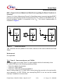
Errata Sheet
V 2.1, 2004-09
Device
C504-2R,
C504-L
Marking/Step
Step AC, AC-T*
Package
P-MQFP-44
This Errata Sheet describes the deviations from the current user documentation.
The module oriented classification and numbering system uses an ascending sequence
over several derivatives, including already solved deviations. So gaps inside this
enumeration can occur.
Current Documentation
• C504 User's Manual 11.97
• C504 Data Sheet May 2000
• Instruction Set Manual 07.2000
Note: Devices marked with EES- or ES are engineering samples which may not be
completely tested in all functional and electrical characteristics, therefore they
should be used for evaluation only.
Note: * The only difference between AC and AC-T steps is the production line. AC-T is
produced by TSMC.
The specific test conditions for EES and ES are documented in a separate Status Sheet.
Contents
Section . . . . . . . . . . . . . . . . . . . . . . . . . . . . . . . . . . . . . . . . . . . . . . . . . . . . . . . . . . Page
History List/Change Summary . . . . . . . . . . . . . . . . . . . . . . . . . . . . . . . . . . . . . . . . . .2
Functional Deviations . . . . . . . . . . . . . . . . . . . . . . . . . . . . . . . . . . . . . . . . . . . . . . . . .4
Deviations from Electrical- and Timing Specification. . . . . . . . . . . . . . . . . . . . . . . .8
Application Hints . . . . . . . . . . . . . . . . . . . . . . . . . . . . . . . . . . . . . . . . . . . . . . . . . . . .10
Errata Sheet, C504-2R, C504-L, Step AC, AC-T
1/10
K. Yang, V 2.1, 2004-09
Errata Sheet
History List/Change Summary
1
History List/Change Summary
(since last CPU Step AB, previous Errata Sheet V2.0)
Table 1
Functional Deviations
Functional
Deviation
Short Description
ADC.1
The Continuous Conversion Mode of ADC is not
functioning
CCU.1
Spike at CCx / COUTx pins
ROM.1
Wrong destination address at AJMP and ACALL
instructions
ROM.2
ROM Verification Mode 1 is inoperable
ROM.3
Using MOVC from external ROM to access the internal
ROM memory is invalid in unprotected ROM Mode
ROM.4
ROM Verification Mode 2 and verification error
signaling at Port 3.5
RST.1
Figure in User’s Manual and Data Sheet regarding the
Reset Circuitries is incorrect
T2.1
Timer 2 - Concurrent Access on T2CON
Table 2
AC/DC Deviations
AC/DC
Deviation
Short Description
DC.1
± 4 LSB Total Unadjusted Error (TUE) of A/D
Converter
DC.2
Minimum supply voltage VCC = 4.75 V at 40 MHz
clock frequency
DC.3
Maximum value of -70 µA for the logic 0 input
current (Ports 1, 2, 3)
DC.8
Minimum value of -3 µA for the logic 0 input current
(Ports 1, 2, 3)
DC.9
Maximum limit values of the power supply current
(IDD)for Active Mode
Errata Sheet, C504-2R, C504-L, Step AC, AC-T
Fixed
Change
in Step
AC
New
Fixed
in Step
2/10
Change
K. Yang, V 2.1, 2004-09
Errata Sheet
History List/Change Summary
Table 3
Application Hints
Application
Hint
Short Description
Fixed
in Step
Change
None.
Errata Sheet, C504-2R, C504-L, Step AC, AC-T
3/10
K. Yang, V 2.1, 2004-09
Errata Sheet
Functional Deviations
2
Functional Deviations
ADC.1: The Continuous Conversion Mode of ADC is not functioning
In the Continuous Conversion Mode, the ADC can not provide the correct digital output
value corresponding to the analog input voltage. The device can not start the Continuous
Mode.
Workaround:
The Continuous Conversion Mode should only be started by writing ADDATL with
dummy data after the ADM bit (ADCON0.3) has been set.
For example:
........
........
ORL
ADCON0, #00001000b
MOV
ADDATL, #11000000b
.......
CCU.1: Spike at CCx / COUTx pins
A write operation to SFR COINI will cause a spike from low to high level of about 10 ns
width (@ 20 MHz external microcontroller clock) at CCx or/and COUTx, if these pins are
assigned to the CCU in the following way:
• The CCx or/and COUTx pins are programmed as compare output of the CCU
(corresponding bits in SFRs CMSEL0 or CMSEL1 set)
• The COINI register has a “0” in a CCx/COUTx pin related bit position
• The related CCx/COUTx pins are at low level during the write operation to SFR COINI
The occurrence of the spike is independent of the state of compare Timer 1 (running or
stopped).
Workaround:
During initialization of the CCU, the spike can be avoided if COINI is written before
CMSEL0 or CMSEL1 are written. If the CCU is running, COINI should be never written.
If the write operation to COINI is absolutely required. While the CCU is running, an
external low pass filter can be used e.g. to suppress the spike at the CCx / COUTx pins.
Errata Sheet, C504-2R, C504-L, Step AC, AC-T
4/10
K. Yang, V 2.1, 2004-09
Errata Sheet
Functional Deviations
ROM.2: ROM Verification Mode 1 is inoperable
The ROM Verification Mode 1, as described in the C504 User's Manual 06.96 on page
4-8 (or User's Manual 11.97 on page 4-6), is inoperable. This means that it is not
possible to verify the internal ROM content using this specific ROM Verification Mode 1.
Workaround:
The internal ROM contents of C504-2RM parts are verified during device testing using
another verification mode.
ROM.3: Using MOVC from external ROM to access the internal ROM memory is
invalid in unprotected ROM mode.
In the unprotected ROM Mode, the logic state of /EA pin is only latched in the Reset
stage and is not allowed to be changed until performing another Reset. In this case, the
MOVC instruction code executed from the external ROM and accessing to the internal
ROM code bytes is not possible since /EA pin can not be toggled. With MOVC
instructions executed from internal ROM, accessing internal code bytes works as
expected.
Workaround:
None.
ROM.4: ROM Verification Mode 2 and verification error signaling at Port 3.5
For C504-2R ROM version product:
The last block of 16 bytes will always return verification error in the ROM Verification
Mode 2.
Workaround:
None.
Errata Sheet, C504-2R, C504-L, Step AC, AC-T
5/10
K. Yang, V 2.1, 2004-09
Errata Sheet
Functional Deviations
RST.1: Figure in User’s Manual and Data Sheet regarding the Reset Circuitries is
incorrect
Figure 5-1 in User’s Manual and Figure 6 in Data Sheet show incorrectly that the RESET
pin has an internal pullup resistor connected to the VDD. Instead, at the RESET pin, an
internal pulldown resistor is connected to the VSS. The correct implementation is
illustrated in Figure 1.
VDD
VDD
C504
C504
C504
RESET
RESET
+
RESET
&
+
a)
Figure 1
c)
b)
Reset Circuitries
This correction will be updated to the future versions of the User’s Manual and Data
Sheet.
Workaround:
Not applicable
T2.1: Timer 2 - Concurrent Access on T2CON
A problem might occur when Timer 2 is used together with the functionality of the
P1.1/AN1/T2EX pin in the following operating modes:
• Timer 2 as baud rate generator
• Timer 2 in 16-bit capture
• Timer 2 in 16-bit auto-reload with DCEN=0
When a falling edge on P1.1/AN1/T2EX occurs during the execution of a read-modifywrite instruction on SFR T2CON, the interrupt flag EXF2 is not set and the related
interrupt, if enabled, is not executed.
Errata Sheet, C504-2R, C504-L, Step AC, AC-T
6/10
K. Yang, V 2.1, 2004-09
Errata Sheet
Functional Deviations
Workaround:
When using a read-modify-write instruction on T2CON, it must be checked (e.g. by
software) whether a high-to-low signal transition occurred at pin P1.1/AN1/T2EX during
the execution of the read-modify-write instruction. This can be achieved by polling the
level on P1.1/AN1/T2EX before and after the read-modify-write instruction. Timer 2
interrupt has to be disabled during the polling sequence. If a high-to-low signal transition
is detected at P1.1/AN1/T2EX, the interrupt EXF2 flag can be set by software.
The following assembly program demonstrates a possible software workaround:
workaround:
clr
et2
;
jnb
p1.1, rmw1
;
rmw2:
orl
t2con, #xxh
;
jnb
p1.1, force_t2int;
setb et2
;
sjmp go_on
;
force_t2int:
setb exf2
;
setb et2
;
sjmp go_on
;
rmw1:
orl
t2con, #xxh
;
setb et2
;
go_on:
......
......
disable t2 interrupt
normal rmw if pin is already low
rmw on t2con
force t2int if p1.1 low now
enable t2 int again
go_on, no falling p1.1-edge occurred
set request flag
enable t2 int again, force interrupt exf2
go_on, falling edge occured within rmw
rmw on t2con
enable t2 int again & go_on
Note: If the external signal on P1.1/AN1/T2EX is a short pulse, the pulse width has to be
at least 3 instruction cycles long. Otherwise, the polling sequence of the pin cannot
recognize the high-to-low signal transition.
Errata Sheet, C504-2R, C504-L, Step AC, AC-T
7/10
K. Yang, V 2.1, 2004-09
Errata Sheet
Deviations from Electrical- and Timing Specification
3
Deviations from Electrical- and Timing Specification
DC.1: ± 4 LSB Total Unadjusted Error (TUE) of A/D Converter
The total unadjusted error of the A/D Converter does not meet the specified value of the
DC characteristics. The value for TUE is limited as follows:
TUE = ± 4 LSB
in the VIN range: VSS < VIN < VCC
Workaround:
None.
DC.2: Minimum supply voltage VCC = 4.75 V at 40 MHz clock frequency
The minimum rating for supply voltage at 40 MHz clock frequency is VCC = 4.75 V for all
operating temperatures (for C504-L40/C504-2R40 only).
Workaround:
None.
DC.3: Maximum value of - 70 µA for the logic 0 input current (Ports 1, 2, 3)
The maximum value of the logic 0 input current for ports 1, 2, and 3 is higher than the
specified value:
IIL max = - 70 µA
(instead of - 50 µA)
Workaround:
None.
DC.8: Minimum value of - 3 µA for the logic 0 input current (Ports 1, 2, 3)
The minimum value of the logic 0 input current for ports 1, 2, and 3 is lower than the
specified value:
IIL min. = - 3 µA
(instead of - 10 µA)
Workaround:
None.
Errata Sheet, C504-2R, C504-L, Step AC, AC-T
8/10
K. Yang, V 2.1, 2004-09
Errata Sheet
Deviations from Electrical- and Timing Specification
DC.9: Maximum limit values of the power supply current (IDD) for Active Mode
The maximum limit values of the power supply current (IDD) for Active Mode are shown
in the table below, instead of the specified values stated in the Data Sheet.
Power Supply Current
Parameter
Active Mode
C504-2R/
C504-L
Symbol
Maximum Limit Values Unit
24 MHz
IDD
37.57
mA
40 MHz
IDD
60.89
mA
Workaround:
None.
Errata Sheet, C504-2R, C504-L, Step AC, AC-T
9/10
K. Yang, V 2.1, 2004-09
Errata Sheet
Application Hints
4
Application Hints
No application hints for this step.
Application Support Group, Singapore
Errata Sheet, C504-2R, C504-L, Step AC, AC-T
10/10
K. Yang, V 2.1, 2004-09