1
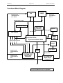
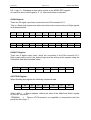
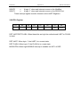
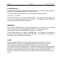
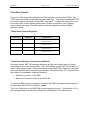
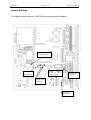
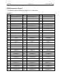
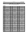
Preliminary
SMT128
User Manual
Preliminary
Page 2 of 15
SMT128 User Manual
Revision History
Date
Comments
Engineer
Version
13/6/00
Initial version
AJP
1.0
05/9/00
Second Revision
AJP
1.1
07/01/02
Modifications
AJP
1.2
26/02/02
Several Modifications Made
BM
1.3
Preliminary
Page 3 of 15
SMT128 User Manual
Table of Contents
Revision History.......................................................................................................... 2
Table of Contents ....................................................................................................... 3
Introduction................................................................................................................. 4
Functional Block Diagram........................................................................................... 5
Memory Map............................................................................................................... 6
Virtex Registers .......................................................................................................... 6
WDOG RST ............................................................................................................ 6
WDOG ENABLE ..................................................................................................... 6
DIGIN Register........................................................................................................ 7
DIGOUT Register.................................................................................................... 7
VSTATUS Register ................................................................................................. 7
VCNTRL Register ................................................................................................... 8
FLASH Memory .......................................................................................................... 9
EEPROM .................................................................................................................... 9
UART.......................................................................................................................... 9
Com Port Control...................................................................................................... 10
Token Reset Control Registers ............................................................................. 10
Token Reset Software Functions and Method ...................................................... 10
J21,J24 – Virtext boot mode ................................................................................. 11
J21,J24 – Virtext boot mode ................................................................................. 12
J30 – Flash Write Protect...................................................................................... 12
J27,J28 – Com CPLD User I/O ............................................................................. 12
DIN Connector Pinout............................................................................................... 13
DIN PL1 ................................................................................................................ 13
DIN PL2 ................................................................................................................ 14
Preliminary
Page 4 of 15
SMT128 User Manual
Introduction
The SMT128 is a 3 site TIM carrier card with additional customised features, acting
as a supports environment for a DSP TIM and two other peripheral TIM’s. The
various ‘on-board’ peripherals available on the motherboard are listed below.
•
TIM Site 1: Standard Single width TIM site capable of accepting any TIM
compatible card. For the most embedded projects this can be a DSP processing
card. It has full COMM-PORT and Global Expansion Bus interconnectivity. The
site is also capable of accepting C6x based DSP although only four com-ports are
available. These com-ports are routed to the PL2 DIN connector for inter-module
communication via com-ports (0,1,3,4) via a buffer CPLD.
•
TIM Site 2: Standard Single Width TIM site with additional 26 way and 24 way
IDC sockets, see mechanical/electrical information. This is designed to accept
the SMT397 12 channel differential ADC/DAC TIM although other peripheral
TIM’s can be used.
•
TIM Site 3: Standard Single Width TIM site with two additional 24 way IDC
sockets, see mechanical/electrical information. This is designed to accept the
SMT392 4 channel RS422 Transceiver/Digital IO TIM although other peripheral
TIM’s can be used..
•
Motherboard Resources/Peripherals
•
Power Supplies 3.3V, 5V +-15v all generated.
•
Control FPGA
•
Digital Inputs/Outputs
•
Power Monitor & Watchdog
•
8K bytes of EEprom that can be used to store application parameters.
•
JTAG Port
•
4Mbit FLASH ram for application Software
•
Quad UART with links to the DIN connectors and also one to an RS232
connector.
The Motherboard has 2 DIN4162 connectors placed at the back of the board which
conform with the VME mechanical specifications. The Pin-out out the connectors is
given later in this specification. Four of the DSP com-ports are available on the back
panel connectors to allow multiple boards to communicate with each other. Each
com-port has a control circuitry to allow motherboard in a system to be ‘hot
swappable’.
Preliminary
Page 5 of 15
SMT128 User Manual
Functional Block Diagram
Analogue
TIM Site
RS422 TIM
Site
Digital signal
connections to
PL1 & PL2
Analogue
connections
to PL1
Global Resource Bus
Front Panel JTAG
DSP & PSU
Watchdog
Eprom
14 TTL I/O’s
DSP TIM Site
24 TTL I/O’s
4Mbyte
FLASH
RAM
Controller FPGA
DSP Comm-Port PAU
0
1 3
Spartan XC2S100 FG256
4
Power
Supplys
Quad
UART
Digital signal
connections to
PL2
Digital signal
connections to
PL1
PL2 DIN41612
Back-Panel
Connector
Key Switch
Virtex to PL1
connections
PL1 DIN41612
Back-Panel
Connector
Front Panel Maintenance Port (RS232)
Preliminary
Page 6 of 15
SMT128 User Manual
Memory Map
There are four basic motherboard resources, Virtex internal registers, FLASH RAM,
EEPROM and UART. Each of these resources is explained in the following sections.
Register
Global Address
Description
FLASH Memory
0xA0000000 -> 0xA003FFFF
FLASH Application/Boot space
EEPROM
0xA8000000 -> 0xA80000FF
8 –bit Non-volatile parameter storage
Virtex Registers
0xB0000000 -> 0xB0000007
See Description below
UART 1
0xB8000000 -> 0xB8000007
ModBus interface
UART 2
0xB8000008 -> 0xB800000F
RS232 interface
Virtex Registers
Register
Global Address
Description
WDOG RST
0xB0000000
Writing to this register resets the watchdog
timer.
WDOG ENABLE
0xB0000001
Enables/Disables WDOG timer
DIGIN Register
0xB0000002
Read only, D0..D21 is state of digital I/P’s
DIGOUT Register
0xB0000003
Drives the digital O/P signals
VSTATUS
0xB0000004
Virtex Status Register
VCNTRL
0xB0000005
Virtex Control Register
WDOG RST
When the Watchdog timer is enabled (See WDOG ENABLE). This register must be
written to with a period of less than 1.6 seconds. If the register is not written to within
this period a global reset is initiated and the FAULT LED is activated. The fault LED
goes out next time the WDOG RST register is written to.
WDOG ENABLE
When writing to this register the level of the data line D0 selects either an internal
oscillator or a WDOG RST signal for the watchdog timer.
D0 -> logic 0 = Watchdog is reset using an internal oscillator.
Preliminary
Page 7 of 15
SMT128 User Manual
D0 -> logic 1 = Watchdog is reset using a write to the WDOG RST register.
At reset the value of this signal is ‘0’ i.e. internal oscillator is selected.
DIGIN Register
There are 22 digital input lines connected to the DIN connector PL1.
This is a Read-only register and when read returns the current value on DigIn signals
as illustrated below.
D21
D20
D19
D18
D17
D16
D15
D14
D13
D12
D11
DigIn22
DigIn21
DigIn20
DigIn19
DigIn18
DigIn17
DigIn16
DigIn15
DigIn14
DigIn13
DigIn12
D10
D9
D8
D7
D6
D5
D4
D3
D2
D1
D0
DigIn11
DigIn10
DigIn9
DigIn8
DigIn7
DigIn6
DigIn5
DigIn4
DigIn3
DigIn2
DigIn1
DIGOUT Register
There are 8 digital output lines, which are connected to the DIN connector PL1.
Each output can be set to the desired logic level by writing to this register using the
Global Bus data bits illustrated below.
D7
D6
D5
D4
D3
D2
D1
D0
DigOut8
DigOut7
DigOut6
DigOut5
DigOut4
DigOut3
DigOut2
DigOut1
VSTATUS Register
When Reading this register the following values are read.
D7
D6
D5
D4
D3
D2
D1
D0
X
X
X
S0INT1
S0INT0
TERMINAL
Addr1
Addr0
Addr0, Addr1 -> Board address, reflects the state of the Addr0 and Addr1 signals
on the PL1 connector.
TERMINAL ->
When a VT100 terminal, or compatible, is connected to the front
panel this bit is logic ‘1’.
Preliminary
Page 8 of 15
SMT128 User Manual
S0INT0
->
A logic ‘1’ when and interrupt occurs on the ModBus.
S0INT1
->
A logic ‘1’ when and interrupt occurs on the RS232 Port.
These interrupt signals must be cleared via the UART Registers.
VCNTRL Register
D7
D6
D5
D4
D3
D2
D1
D0
X
X
X
X
X
MODINTEN
RST
UART
RST
FLASH
RST UART/RST FLASH: When these bits are high the motherboard UART or FLASH
is reset.
RST UART: When logic ‘1’ the UART is in a reset state.
RST FLASH: When logic ‘0’ the FLASH is in a reset state
MODINTEN: When high MODBUS interrupt is enabled on IIOF1 of DSP.
Preliminary
Page 9 of 15
SMT128 User Manual
FLASH Memory
The SMT128 has 4Mbit of boot block flash memory. This allows larger application
programs to be stored and loaded and run by the DSP.
The motherboard resource is located at the following address locations:
0xA0000000 -> 0xA003FFFF
The FLASH device is a Hyundai HY29F400BT-70. This requires 4 wait states to be
set up for the global bus transfer from the DSP. The operation of the FLASH is
described in the manufacturers data sheet.
EEPROM
An 8k byte of EEPROM allows program parameters to be stored in a non-volatile
media. Data stored is just the lower 8 bits (D0.D7) of the global data lines.
The memory range for the EEPROM is 0xA8000000 -> 0xA80000FF
The EEPROM device is a ATMEL AT28C64E-12SC. This requires 6 wait states to
be set up for the global bus transfer from the DSP. The operation of the device is
described in the manufacturers data sheet.
UART
The Motherboard UART is a Oxford devices OX16C954 quad device it uses a
40MHz crystal to generate a programmable baud rates. One of the outputs is
connected to the front panel via an RS232 driver to allow VT100 terminal
communications with the motherboard. A differential receive and transmit signals are
connected to the back panel DIN41612 connector, via an ADM1485, at RS422 levels
to allow a remote modbus protocol link. The fourth output of the Quad UART is
unused. For details on setting up the UART please refer to the Oxford devices data
sheet
Preliminary
Page 10 of 15
SMT128 User Manual
Com Port Control
Four of the C6x com-ports connect to the DIN connector via a control CPLD. The
CPLD acts as a buffer for the Data com-port data lines. This allows multiple SMT128
to communicate in a system via the DSP’s com-ports. To allow the state of the comport to be reset, to their default states after a power-up condition, four registers
resources are provided. The table below shows the registers and their Global
address values.
Token Reset Control Registers
Com-Port
Address
Operations
Com 0
0xF0000000
Write 0x1 to reset the token for the comport then write a ‘0’
Com 1
0xF0000001
Write 0x1 to reset the token for the comport then write a ‘0’
Com 3
0xF0000002
Write 0x1 to reset the token for the comport then write a ‘0’
Com 4
0xF0000003
Write 0x1 to reset the token for the comport then write a ‘0’
Token Reset Software Functions and Method
On power-up the SMT128 com-port directions will be set to either Input or Output
depending on their com-port number. The CPLD buffers on the SMT128 will also be
reset to their correct state. When connecting multiple SMT128’s together in a system
there are situation when com-ports may become unsynchronised. To re-synchronise
the system it is necessary to do the following.
•
Reset the com-port in the DSP.
•
Reset the Com-port buffer on the SMT128.
To reset the DSP’s com-port register a write to the DSP’s com-port control register is
required (see SMT335 User Guide of details).
The Com-Port buffer on the SMT128 can be reset by writing a ‘1’ followed by a ‘0’ to
the corresponding com-port token Reset Control Register in the table above.
Preliminary
Page 11 of 15
SMT128 User Manual
Jumper Settings
The diagram below shows the SMT128 with jumper positions labelled.
J19:Pin 1 For XChecker Header
J29,J31:
FLASH
Protect for other
Makes (unused)
J30 : FLASH
Write Protect
J27,J28: User
IO to CPLD
J21,J24: Virtex
Boot Mode
J25: Pin 1 for
JTAG Header
Preliminary
Page 12 of 15
SMT128 User Manual
J21, J24 – Virtex boot mode
With J21 in and J24 out, the SMT128 will boot from a serial prom. When booting
from X-checker header remove J21. J24 with reset the serial prom when in and may
be fitted when booting from x-checker if the serial prom is still fitted in the IC socket.
J30 – Flash Write Protect
This jumper must be fitted to permit write cycles to be accepted by the SMT128
FLASH memory.
J27, J28 – Com CPLD User I/O
These are connected to the SMT128 com-port CPLD for future expansion.
Preliminary
Page 13 of 15
SMT128 User Manual
DIN Connector Pinout
The following tables define the DIN 41612 pin allocation :
DIN PL1
a
Description
b
Description
c
Description
1
ChX/Analogue Input 1+
1
ChX/Analogue Out 1+
1
ChX/Analogue Input 1-
2
ChX/Analogue Input 2+
2
ChX/Analogue Out 1-
2
ChX/Analogue Input 2-
3
ChX/Analogue Input 3+
3
ChX/Analogue Out 2+
3
ChX/Analogue Input 3-
4
ChX/Analogue Input 4+
4
ChX/Analogue Out 2-
4
ChX/Analogue Input 4-
5
ChX/Analogue Input 5+
5
ChX/Analogue Out 3+
5
ChX/Analogue Input 5-
6
ChX/Analogue Input 1+
6
ChX/Analogue Out 3-
6
ChX/Analogue Input 1-
7
ChX/Analogue Input 1+
7
ChX/Analogue Out 4+
7
ChX/Analogue Input 1-
8
ChX/Analogue Input 8+
8
ChX/Analogue Out 4-
8
ChX/Analogue Input 8-
9
ChX/Analogue Input 9+
9
ChX/Pulse In 1+
9
ChX/Analogue Input 9-
10
ChX/Analogue Input 10+
10
ChX/Pulse In 1-
10
ChX/Analogue Input 10-
11
ChX/Analogue Input 11+
11
ChX/Pulse In 2+
11
ChX/Analogue Input 11-
12
ChX/Analogue Input 12+
12
ChX/Pulse In 2-
12
ChX/Analogue Input 12-
13
Sync
13
ChX/Spare 1
13
ChX/Spare 2
14
Digin 1
14
Digin 2
14
Digin 3
15
Digin 4
15
Digin 5
15
Digin 6
16
Digin 7
16
Digin 8
16
Digin 9
17
Digin 10
17
Digin 11
17
Digin 12
18
Digin 13
18
Digin 14
18
Digin 15
19
Digin 16
19
Digin 17
19
Digin 18
20
Digin 19
20
Digin 20
20
Digin 21
21
Addr 0
21
Addr 1
21
Digin 22
22
ChX/Digout 1
22
ChX/Digout 2
22
ChX/Digout 3
23
ChX/Digout 4
23
ChX/Digout 5
23
ChX/Digout 6
24
ChX/Digout 7
24
ChX/Digout 8
24
5V Out
25
Not used
25
Not used
25
Not used
26
ModBus Tx +
26
Not used
26
ModBus Tx -
27
ModBus Rx +
27
ChX/Digout 9
27
ModBus Rx -
28
ChX/Digin 23
28
ChX/Digout 10
28
ChX/Digin 24
29
ChX/Digin 25
29
ChX/Digout 11
29
ChX/Digin 26
30
ChX/Digin 27
30
ChX/Digout 12
30
ChX/Digin 28
31
ChX/Digin 29
31
ChX/Digout 13
31
ChX/Digin 30
Preliminary
32
Page 14 of 15
ChX/Digout 15
32
ChX/Digout 14
SMT128 User Manual
32
ChX/Digout 16
Table 1: PL1 DIN 41612 pin allocation
DIN PL2
a
Description
b
Description
c
Description
1
ChX/Digout 19
1
Not used
1
ChX/Digout 20
2
ChX/Digout 21
2
ChX/Digout 17
2
ChX/Digout 22
3
ChX/Digout 23
3
ChX/Digout 18
3
ChX/Digout 24
4
ChX/Digout 25
4
ChX/RS485Tx1+
4
ChX/Digout 26
5
ChX/Digout 27
5
ChX/RS485Tx1-
5
ChX/Digout 28
6
ChX/Digout 29
6
ChX/RS485Tx1+
6
ChX/Digout 30
7
ChX/Digout 31
7
ChX/RS485Tx1-
7
ChX/Digout 32
8
ChX/RS422Tx1+
8
ChX/RS485Tx2+
8
ChX/RS422Tx1-
9
ChX/RS422Rx1+
9
ChX/RS485Tx2-
9
ChX/RS422Rx1-
10
ChX/RS422Tx2+
10
ChX/RS485Tx2+
10
ChX/RS422Tx2-
11
ChX/RS422Rx2+
11
ChX/RS485Tx2-
11
ChX/RS422Rx2-
12
Not used
12
Not used
12
Not used
13
D0C0
13
!CREQ
13
D0C3
14
D1C0
14
!C0ACK
14
D1C3
15
D2C0
15
!C0STRB
15
D2C3
16
D3C0
16
!C0RDY
16
D3C3
17
D4C0
17
!C3REQ
17
D4C3
18
D5C0
18
!C3ACK
18
D5C3
19
D6C0
19
!C3STRB
19
D6C3
20
D7C0
20
!C3RDY
20
D7C3
21
D0C1
21
!C1REQ
21
D0C5
22
D1C1
22
!C1ACK
22
D1C5
23
D2C1
23
!C1STRB
23
D2C5
24
D3C1
24
!C1RDY
24
D3C5
25
D4C1
25
!C5REQ
25
D4C5
26
D5C1
26
!C5ACK
26
D5C5
27
D6C1
27
!C5STRB
27
D6C5
28
D7C1
28
!C5RDY
28
D7C5
29
ChX/24V_Out
29
ChX/24V_Out
29
ChX/24V_Out
30
24V A
30
24V A
30
24V A
31
24V B
31
24V B
31
24V B
Preliminary
32
Page 15 of 15
Gnd/0V
32
Gnd/0V
SMT128 User Manual
32
Table 2: PL2 DIN 41612 pin allocation
Gnd/0V