1
Freescale Semiconductor
Application Note
Document Number: AN2916
Rev. 0, 07/2005
eDINK for MPC8560ADS
by
Ahsan Kabir
NCSD
Freescale Semiconductor, Inc.
Austin, TX
eDINK (e500 core Demonstrative Interactive Nanokernel),
an enabling and debugging tool for e500 processors, has
been ported to the MPC8560ADS pilot board. Most of the
work was performed on the low level BOOT ROM like CPU
initialization, FLASH configuration, DDR configuration,
setting the I/O, etc. After eDINK comes up, the user will see
the active eDINK command prompt. Typing ‘help’ at the
command prompt will bring up several commands, which
are a superset of all the commands that were built up over
time and support many different boards. eDINK running on
the MPC8560ADS board supports only a subset of all these
listed commands. See Section 7, “Supported Commands,”
for more information.
1
Introduction
This release of eDINK has been ported from eDINK running
on a platform simulator. The following features are added in
this release:
• support for MPC8560ADS board in MPC8540 mode
only
• either the DDR memory or SDRAM memory in the
local bus can act as system memory
© Freescale Semiconductor, Inc., 2004, 2005. All rights reserved.
Contents
1. Introduction . . . . . . . . . . . . . . . . . . . . . . . . . . . . . . . . . 1
2. Programming the FLASH with the Shipped Working
eDINK Binary File (edink.bin) 2
3. Recompiling the SOURCE . . . . . . . . . . . . . . . . . . . . . 5
4. Board Settings –Jumpers and Switches . . . . . . . . . . . 5
5. Preparing to Run eDINK . . . . . . . . . . . . . . . . . . . . . . 7
6. Default Program Settings . . . . . . . . . . . . . . . . . . . . . . 9
8. Figures . . . . . . . . . . . . . . . . . . . . . . . . . . . . . . . . . . . . 6
8. Conclusion . . . . . . . . . . . . . . . . . . . . . . . . . . . . . . . . 10
Programming the FLASH with the Shipped Working eDINK Binary File (edink.bin)
•
•
•
•
•
•
•
Level 1 data and instruction cache are turned on
Level 2 unified cache is turned on
Branch prediction is enabled
Address streaming is enabled
DDR dll patch has been applied
local bus dll patch has been added
Serial driver provided is for DUART only, there is no CPM based serial driver. Therefore, eDINK
is currently limited to run in MPC8540 mode only.
The source tree for eDINK can be obtained from the DINK website. The limited and full source tree for
this distribution is available from the DINK website. Extracting the full source tree will provide the
following:
• src/: directory which contains all the eDINK related source files
• save_obj/: directory which contains the networking object files (make sure to copy these object
files to obj/ directory before compiling)
• obj/: empty directory which is used during compilation
• makefile: note that based on cross compiler locations, these environment variables may have to be
changed - PREFIX, LDFLAGS, AS, CC, LD, OBJCOPYCFLAGS, AFLAGS, LDFLAGS. This
makefile should be reviewed carefully before recompilation.
• edink.bin, edink.src, edink: the functional binary/srec/elf file which can be programmed into the
on-board FLASH of the MPC8560ADS board. To do so without compiling, program FLASH with
any one of these images which is supported by the FLASH programmer.
• edink-flash.xml: FLASH programmer configuration file to be used with CodeWarrior 1.1
(CodeWarrior Development Studio, PowerQUICC III Edition, version 1.0.4, Build 40406). Note
that the specific build and version number may not be necessary in order to use this file.
2
Programming the FLASH with the Shipped Working
eDINK Binary File (edink.bin)
The last 4MB of the 16MB on board FLASH of the MPC8560ADS board is used to program the eDINK
image. This working image can be programmed using any standard FLASH Programmer Utility that can
communicate with the MPC8560ADS pilot board. Note that the FLASH Programmer utility should
support programming the raw binary file.
The following steps are involved in programming the on-board FLASH:
1. Suppose that the starting address of the FLASH is 0xFF000000, then the last 4MB of FLASH area
starts at 0xFFC00000 and the end address of the FLASH is 0xFFFFFFFF
2. Erase only the last 4MB (i.e. from 0xFFC00000 to 0xFFFFFFFF)
3. Program the edink-working.bin image starting at address 0xFFC00000
4. Note that the image size in this case is 0x400000 (which is 4MB)
eDINK for MPC8560ADS, Rev. 0
2
Freescale Semiconductor
Programming the FLASH with the Shipped Working eDINK Binary File (edink.bin)
2.1
Programming edink.bin with CodeWarrior
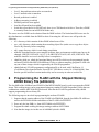
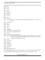
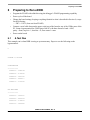
Based upon the above description, a specific example of FLASH programming using CodeWarrior 1.1
(CodeWarrior Development Studio, PowerQUICC III Edition, version 1.0.4, Build 40406) is provided
below. Also, the edink-flash.xml file is provided with this release, which consists of the settings required
for the FLASH programmer. In order to make use of this file, first invoke the FLASH programmer by
clicking on ‘Tools->Flash Programmer’. Then use the ‘Load Settings…’ tab and point to the
edink-flash.xml file. CodeWarrior FLASH Programmer window captures are provided in Figure 1,
Figure 2, Figure 3, and Figure 4 for reference.
Figure 1. Target Configuration for FLASH Programmer
eDINK for MPC8560ADS, Rev. 0
Freescale Semiconductor
3
Programming the FLASH with the Shipped Working eDINK Binary File (edink.bin)
Figure 2. FLASH Device Configuration for FLASH Programmer
Figure 3. Erase/Blank Check Tab for FLASH Programmer
eDINK for MPC8560ADS, Rev. 0
4
Freescale Semiconductor
Recompiling the SOURCE
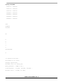
Figure 4. Program/Verify Tab for FLASH Programmer
3
Recompiling the SOURCE
Extract the full source tree in the $EDINK_BASE directory.
src, save_obj, and obj directories, which contain the source codes and object files required to build eDINK
executable, will exist after extraction.
Also, the makefile will be located in the $EDINK_BASE.
Modify the makefile so that it points to the toolchain. Note that in order to build eDINK executable, a
PowerPC EABI toolchain modified to support e500 is required.
%cp save_obj/* obj/
%make
make will generate the edink.bin file in obj/ directory. It will also generate the elf binary (eDINK) and
s-record (edink.src).
4
Board Settings –Jumpers and Switches
In order to program the FLASH, some kind of a debugger needs to be run and communicated over the
COP/JTAG interface. The following switch settings are recommended when the debugger is run. For each
of the switch settings, the value of pin 1 is shown first, followed by the value of pin 2, then 3, and so on.
Here, 0 means “ON” and 1 means “OFF”. Please refer to the MPC8540ADS Pilot1 Quick Reference Guide
document that comes with the MPC8560ADS board for a detailed description of the switches on board.
eDINK for MPC8560ADS, Rev. 0
Freescale Semiconductor
5
Board Settings –Jumpers and Switches
Also, note that the switch settings mentioned here are one of the many possible configurations for which
eDINK runs.
SW1 = 111111
SW2 = 111111
SW3 = 001111
SW4 = 00010011
SW5 = 0011111111
SW6 = 01001011
SW7 = 11111111
SW9 = 10
SW10 = 01111100
SW11 = 10100100 (position 2 = 0/1 for MPC8540 mode/MPC8560 mode); (position 7 = 0/1 for rev2/rev1
silicon)
SW12 = 1001100000
SW13 = 1000
SW14 = 0000
SW15 = 011101
SW16 = 0000
SW17 = 10000100
SW18 = push button; no configuration needed
SW19 = push button; no configuration needed
SW20 = 011011
SW21 = push button; no configuration needed
SW22 = 0101 (if CodeWarrior with PowerTAP Pro is being used; for any other debugger type, find out
what this switch would be from MPC8540_ADS_Quick_Guide_rev1.9.doc, which is
shipped with the MPC8560ADS board)
SW23 = 010110
SW24 = push button
SW25 = 011110
SW26 = push button
SW27 = push button
SW28 = push button
SW29 = 0010
SW30 = not mounted (optional)
For FLASH programming, also make sure that J2 jumper is set to “EN”. This will ensure that the FLASH
can be programmed. The FLASH programming will not be successful if this jumper is “DIS”.
eDINK for MPC8560ADS, Rev. 0
6
Freescale Semiconductor
Preparing to Run eDINK
5
Preparing to Run eDINK
•
•
•
•
•
5.1
Program the FLASH with edink.bin using the debugger’s FLASH programming capability
Power cycle off the board
Change the board settings, keeping everything identical to what is described in Section 4, except
for the following:
— SW3 = 111111 (boot out from FLASH)
Connect a serial cable between the upper serial port of the board to any of the COMx ports of the
PC. Setup a hyperterminal for COMx port of the PC with these features: baud = 9600,
parity = none, stop bit = 1, data bits = 8, flow control = none
Power on the board
A Test Run
This example run is when DDR is acting as system memory. Expect to see the following on the
hyperterminal:
G
CONSOLE I/O ACTIVE
CONFIGURATION
=============
FC0E0000 = 00460148
FC0E0004 = 87330000
FC0E0008 = 00010000
FC0E000C = 83830377
FC0E0010 = 07000000
DDR REGISTERS
=============
FC002000 = 00000007
FC002080 = 80000002
FC002108 = 37344321
FC00210C = 00000800
eDINK for MPC8560ADS, Rev. 0
Freescale Semiconductor
7
Preparing to Run eDINK
FC002110 = C2000000
FC002118 = 00000062
FC002124 = 05200100
FC002F00 = 00000000
FC002F04 = 00000000
FC002F08 = 00000018
FC002F0C = 00000000
COPY
000BC000
00100000
OK
R
R
S
T
U
VGO=000036A4
W
I/O system initialized...
Environment is not valid...
Skipping system setup...
RealTime Clock: not running/set.
Memory Enabled: [ 128MB at CL=0 ]
Caches Enabled: [ L1I(32K), L1D(32K), L2(256K) ]
Register Inits: [ 32 GPRs, 227 SPRs ]
eDINK for MPC8560ADS, Rev. 0
8
Freescale Semiconductor
Default Program Settings
##
##
##
##
##
##
##
######
##
#######
##
##
#######
##
##
##
##
##
##
##
##
##
########
##
##
##
##
##
######
##
##
##
##
##
##
##
##
##
##
##
######
######
##
##
##
Version : 13.1.1, GCC Build
Released : May 13, 2003 Built on Jun 30 2004 14:41:10
Ported by
: Freescale’s NCSD Applications Group, Austin, TX
System : MPC8560ADS Evaluation Board
IDProc : PVR=8020 BUS=3ns (133330kHz)
Processor : MPC8540 V1.0 @ 800 MHz, 266 MHz CCB, 133 MHz memory, 66 MHz PCI
Memory : 128MB at CL=0
Copyright Freescale Inc. 1993-2003
Refer to `history.c' for release info, changes, errata and fixes.
EDINK[MPC8540] {1} >>
6
Default Program Settings
The code on AS IS basis would use the DDR as system memory. Do the following to use local bus SDRAM
instead:
• Uncomment out “#define LOCAL_SDRAM_AS_SYS_MEM”
• Comment out “//#define DDR_AS_SYS_MEM”
When DDR is selected as system memory, DDR memory testing can also be selected before copying data
and text section from FLASH memory to DDR memory. Note that DDR testing will drastically increase
boot up time. It takes about 30–40 minutes to boot up with the DDR memory test enabled. In order to
provision for DDR memory test do the following:
• Uncomment “//#define DDR_MEMORY_TEST”
eDINK for MPC8560ADS, Rev. 0
Freescale Semiconductor
9
Supported Commands
Note that LOCAL_SDRAM_AS_SYS_MEM and DDR_AS_SYS_MEM should not be defined
simultaneously.
For a complete description of the memory map for eDINK, please refer to the ‘Creating eDINK for
DINK32 Code using the e500 ISS’ application note located at online at http://www.freescale.com/files/
netcomm/doc/app_note/AN2336.pdf.
7
Supported Commands
Following is the list of all the commands that do not work. For a complete description of these commands,
please refer to DINK32 User’s Manual, located online at http://www.freescale.com/files/soft_dev_tools/
doc/ref_manual/DINK32UM.pdf.
Commands that do not work on MPC8560ADS platform are as follows:
BM, DEV, ENV, FU, ID, NM, PCF, PMAPPER, RMN, SB, TE, TM, W, BO, CRC, FS, LO, MI, PD, PM,
PNG, RST, TR, TI, SH, STTY, TAU.
8
Conclusion
The MPC8560ADS board can be used to run the eDINK that is created for MPC8540 processor. This
eDINK has a lot of optimization features turned on. Running applications under this eDINK environment
have been verified. This eDINK could be used to run benchmark applications because of the many
optimization features enabled. Since eDINK for MPC8540 is ported from eDINK for e500 ISS, it is
worthwhile to look into this application note ‘Creating eDINK for DINK32 Code using the e500 ISS’
located online at http://www.freescale.com/files/netcomm/doc/app_note/AN2336.pdf. Also, the reader
may want to refer to the ‘DINK32 PowerPC Debugger User’s Manual’.
eDINK for MPC8560ADS, Rev. 0
10
Freescale Semiconductor
Conclusion
THIS PAGE INTENTIONALLY LEFT BLANK
eDINK for MPC8560ADS, Rev. 0
Freescale Semiconductor
11
How to Reach Us:
Home Page:
www.freescale.com
email:
[email protected]
USA/Europe or Locations Not Listed:
Freescale Semiconductor
Technical Information Center, CH370
1300 N. Alma School Road
Chandler, Arizona 85224
(800) 521-6274
480-768-2130
[email protected]
Europe, Middle East, and Africa:
Freescale Halbleiter Deutschland GmbH
Technical Information Center
Schatzbogen 7
81829 Muenchen, Germany
+44 1296 380 456 (English)
+46 8 52200080 (English)
+49 89 92103 559 (German)
+33 1 69 35 48 48 (French)
[email protected]
Information in this document is provided solely to enable system and software
implementers to use Freescale Semiconductor products. There are no express or
implied copyright licenses granted hereunder to design or fabricate any integrated
circuits or integrated circuits based on the information in this document.
Freescale Semiconductor reserves the right to make changes without further notice to
any products herein. Freescale Semiconductor makes no warranty, representation or
guarantee regarding the suitability of its products for any particular purpose, nor does
Freescale Semiconductor assume any liability arising out of the application or use of
any product or circuit, and specifically disclaims any and all liability, including without
limitation consequential or incidental damages. “Typical” parameters which may be
provided in Freescale Semiconductor data sheets and/or specifications can and do
vary in different applications and actual performance may vary over time. All operating
Japan:
Freescale Semiconductor Japan Ltd.
Headquarters
ARCO Tower 15F
1-8-1, Shimo-Meguro, Meguro-ku
Tokyo 153-0064, Japan
0120 191014
+81 2666 8080
[email protected]
parameters, including “Typicals” must be validated for each customer application by
Asia/Pacific:
Freescale Semiconductor Hong Kong Ltd.
Technical Information Center
2 Dai King Street
Tai Po Industrial Estate,
Tai Po, N.T., Hong Kong
+800 2666 8080
[email protected]
purchase or use Freescale Semiconductor products for any such unintended or
For Literature Requests Only:
Freescale Semiconductor
Literature Distribution Center
P.O. Box 5405
Denver, Colorado 80217
(800) 441-2447
303-675-2140
Fax: 303-675-2150
LDCForFreescaleSemiconductor
@hibbertgroup.com
Document Number: AN2916
Rev. 0
07/2005
customer’s technical experts. Freescale Semiconductor does not convey any license
under its patent rights nor the rights of others. Freescale Semiconductor products are
not designed, intended, or authorized for use as components in systems intended for
surgical implant into the body, or other applications intended to support or sustain life,
or for any other application in which the failure of the Freescale Semiconductor product
could create a situation where personal injury or death may occur. Should Buyer
unauthorized application, Buyer shall indemnify and hold Freescale Semiconductor
and its officers, employees, subsidiaries, affiliates, and distributors harmless against all
claims, costs, damages, and expenses, and reasonable attorney fees arising out of,
directly or indirectly, any claim of personal injury or death associated with such
unintended or unauthorized use, even if such claim alleges that Freescale
Semiconductor was negligent regarding the design or manufacture of the part.
Freescale™ and the Freescale logo are trademarks of Freescale Semiconductor, Inc.
All other product or service names are the property of their respective owners.
© Freescale Semiconductor, Inc., 2004, 2005.