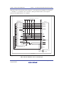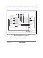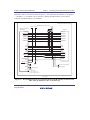
1
User’s Manual
SuperH™ Family E10A-USB Emulator
Additional Document for User’s Manual
Supplementary Information on Using the SH7724
SuperH™ Family
E10A-USB for SH7724
HS7724KCU01HE
All information contained in these materials, including products and product specifications,
represents information on the product at the time of publication and is subject to change by
Renesas Electronics Corporation without notice. Please review the latest information published
by Renesas Electronics Corporation through various means, including the Renesas Electronics
Corporation website (http://www.renesas.com).
www.renesas.com
Rev.2.00
Aug. 2012
Notice
1.
Descriptions of circuits, software and other related information in this document are provided only to illustrate the operation of
semiconductor products and application examples. You are fully responsible for the incorporation of these circuits, software,
and information in the design of your equipment. Renesas Electronics assumes no responsibility for any losses incurred by you
or third parties arising from the use of these circuits, software, or information.
2.
Renesas Electronics has used reasonable care in preparing the information included in this document, but Renesas Electronics
does not warrant that such information is error free. Renesas Electronics assumes no liability whatsoever for any damages
incurred by you resulting from errors in or omissions from the information included herein.
3.
Renesas Electronics does not assume any liability for infringement of patents, copyrights, or other intellectual property rights of
third parties by or arising from the use of Renesas Electronics products or technical information described in this document. No
license, express, implied or otherwise, is granted hereby under any patents, copyrights or other intellectual property rights of
Renesas Electronics or others.
4.
You should not alter, modify, copy, or otherwise misappropriate any Renesas Electronics product, whether in whole or in part.
Renesas Electronics assumes no responsibility for any losses incurred by you or third parties arising from such alteration,
modification, copy or otherwise misappropriation of Renesas Electronics product.
5.
Renesas Electronics products are classified according to the following two quality grades: “Standard” and “High Quality”. The
recommended applications for each Renesas Electronics product depends on the product’s quality grade, as indicated below.
“Standard”:
Computers; office equipment; communications equipment; test and measurement equipment; audio and visual
equipment; home electronic appliances; machine tools; personal electronic equipment; and industrial robots etc.
“High Quality”: Transportation equipment (automobiles, trains, ships, etc.); traffic control systems; anti-disaster systems; anticrime systems; and safety equipment etc.
Renesas Electronics products are neither intended nor authorized for use in products or systems that may pose a direct threat to
human life or bodily injury (artificial life support devices or systems, surgical implantations etc.), or may cause serious property
damages (nuclear reactor control systems, military equipment etc.). You must check the quality grade of each Renesas
Electronics product before using it in a particular application. You may not use any Renesas Electronics product for any
application for which it is not intended. Renesas Electronics shall not be in any way liable for any damages or losses incurred
by you or third parties arising from the use of any Renesas Electronics product for which the product is not intended by Renesas
Electronics.
6.
You should use the Renesas Electronics products described in this document within the range specified by Renesas Electronics,
especially with respect to the maximum rating, operating supply voltage range, movement power voltage range, heat radiation
characteristics, installation and other product characteristics. Renesas Electronics shall have no liability for malfunctions or
damages arising out of the use of Renesas Electronics products beyond such specified ranges.
7.
Although Renesas Electronics endeavors to improve the quality and reliability of its products, semiconductor products have
specific characteristics such as the occurrence of failure at a certain rate and malfunctions under certain use conditions. Further,
Renesas Electronics products are not subject to radiation resistance design. Please be sure to implement safety measures to
guard them against the possibility of physical injury, and injury or damage caused by fire in the event of the failure of a Renesas
Electronics product, such as safety design for hardware and software including but not limited to redundancy, fire control and
malfunction prevention, appropriate treatment for aging degradation or any other appropriate measures. Because the evaluation
of microcomputer software alone is very difficult, please evaluate the safety of the final products or systems manufactured by
you.
8.
Please contact a Renesas Electronics sales office for details as to environmental matters such as the environmental compatibility
of each Renesas Electronics product. Please use Renesas Electronics products in compliance with all applicable laws and
regulations that regulate the inclusion or use of controlled substances, including without limitation, the EU RoHS Directive.
Renesas Electronics assumes no liability for damages or losses occurring as a result of your noncompliance with applicable laws
and regulations.
9.
Renesas Electronics products and technology may not be used for or incorporated into any products or systems whose
manufacture, use, or sale is prohibited under any applicable domestic or foreign laws or regulations. You should not use
Renesas Electronics products or technology described in this document for any purpose relating to military applications or use
by the military, including but not limited to the development of weapons of mass destruction. When exporting the Renesas
Electronics products or technology described in this document, you should comply with the applicable export control laws and
regulations and follow the procedures required by such laws and regulations.
10. It is the responsibility of the buyer or distributor of Renesas Electronics products, who distributes, disposes of, or otherwise
places the product with a third party, to notify such third party in advance of the contents and conditions set forth in this
document, Renesas Electronics assumes no responsibility for any losses incurred by you or third parties as a result of
unauthorized use of Renesas Electronics products.
11. This document may not be reproduced or duplicated in any form, in whole or in part, without prior written consent of Renesas
Electronics.
12. Please contact a Renesas Electronics sales office if you have any questions regarding the information contained in this document
or Renesas Electronics products, or if you have any other inquiries.
(Note 1) “Renesas Electronics” as used in this document means Renesas Electronics Corporation and also includes its majorityowned subsidiaries.
(Note 2) “Renesas Electronics product(s)” means any product developed or manufactured by or for Renesas Electronics.
(2012.4)
Regulatory Compliance Notices
European Union regulatory notices
This product complies with the following EU Directives. (These directives are only valid in the European Union.)
CE Certifications:
• Electromagnetic Compatibility (EMC) Directive 2004/108/EC
EN 55022 Class A
WARNING: This is a Class A product. In a domestic environment this product may
cause radio interference in which case the user may be required to take adequate
measures.
EN 55024
• Information for traceability
• Authorised representative
Name:
Renesas Electronics Corporation
Address:
1753, Shimonumabe, Nakahara-ku, Kawasaki, Kanagawa, 211-8668, Japan
• Manufacturer
Name:
Renesas Solutions Corp.
Address:
Nippon Bldg., 2-6-2, Ote-machi, Chiyoda-ku, Tokyo 100-0004, Japan
• Person responsible for placing on the market
Name:
Renesas Electronics Europe Limited
Address:
Dukes Meadow, Millboard Road, Bourne End, Buckinghamshire, SL8 5FH, U.K.
Environmental Compliance and Certifications:
• Waste Electrical and Electronic Equipment (WEEE) Directive 2002/96/EC
WEEE Marking Notice (European Union Only)
Renesas development tools and products are directly covered by the European Union's Waste
Electrical and Electronic Equipment, (WEEE), Directive 2002/96/EC. As a result, this equipment,
including all accessories, must not be disposed of as household waste but through your locally
recognized recycling or disposal schemes. As part of our commitment to environmental
responsibility Renesas also offers to take back the equipment and has implemented a Tools Product
Recycling Program for customers in Europe. This allows you to return equipment to Renesas for
disposal through our approved Producer Compliance Scheme. To register for the program, click
here “http://www.renesas.com/weee".
United States Regulatory notices on Electromagnetic compatibility
FCC Certifications (United States Only):
This equipment has been tested and found to comply with the limits for a Class A digital device, pursuant to Part
15 of the FCC Rules. These limits are designed to provide reasonable protection against harmful interference
when the equipment is operated in a commercial environment. This equipment generates, uses, and can radiate
radio frequency energy and, if not installed and used in accordance with the instruction manual, may cause
harmful interference to radio communications. Operation of this equipment in a residential area is likely to cause
harmful interference in which case the user will be required to correct the interference at his own expense.
CAUTION:
Changes or modifications not expressly approved by the party responsible for
compliance could void the user's authority to operate the equipment.
Table of Contents
Section 1 Connecting the Emulator with the User System .................................................................... 1
1.1
1.2
1.3
1.4
1.5
Components of the Emulator .................................................................................................................................... 1
Connecting the Emulator with the User System ....................................................................................................... 3
Installing the H-UDI Port Connector on the User System ........................................................................................ 4
Pin Assignments of the H-UDI Port Connector ........................................................................................................ 5
Recommended Circuit between the H-UDI Port Connector and the MPU ............................................................... 9
1.5.1
Recommended Circuit (36-Pin Type) ............................................................................................................ 9
1.5.2
Recommended Circuit (14-Pin Type) .......................................................................................................... 11
1.5.3
Recommended Circuit (38-Pin Type) .......................................................................................................... 13
Section 2 Software Specifications when Using the SH7724 ............................................................... 17
2.1
2.2
Differences between the SH7724 and the Emulator ............................................................................................... 17
Specific Functions for the Emulator when Using the SH7724................................................................................ 22
2.2.1
Event Condition Functions ........................................................................................................................... 22
2.2.2
Trace Functions ............................................................................................................................................ 30
2.2.3
Notes on Using the JTAG (H-UDI) Clock (TCK) and AUD Clock (AUDCK) ........................................... 41
2.2.4
Notes on Setting the [Breakpoint] Dialog Box............................................................................................. 41
2.2.5
Notes on Setting the [Event Condition] Dialog Box and the BREAKCONDITION_ SET Command........ 43
2.2.6
Note on Setting the UBC_MODE Command............................................................................................... 43
2.2.7
Note on Setting the PPC_MODE Command................................................................................................ 43
2.2.8
Performance Measurement Function............................................................................................................ 43
SuperH™ Family E10A-USB Emulator
Section 1 Connecting the Emulator with the User System
Section 1 Connecting the Emulator with the User System
1.1
Components of the Emulator
The emulator supports the SH7724. Table 1.1 lists the components of the emulator.
R20UT2162EJ0200 Rev.2.00
Aug 09, 2012
Page 1 of 56
SuperH™ Family E10A-USB Emulator
Section 1 Connecting the Emulator with the User System
Table 1.1 Components of the Emulator
Classification Component
Hardware
Emulator box
Appearance
Quantity
1
Remarks
HS0005KCU01H:
Depth: 65.0 mm, Width: 97.0 mm,
Height: 20.0 mm, Mass: 72.9 g
or
HS0005KCU02H:
Depth: 65.0 mm, Width: 97.0 mm,
Height: 20.0 mm, Mass: 73.7 g
Software
User system interface
cable
1
14-pin type:
Length: 20 cm, Mass: 33.1 g
User system interface
cable
1
36-pin type:
Length: 20 cm, Mass: 49.2 g
(only for HS0005KCU02H)
USB cable
1
Length: 150 cm, Mass: 50.6 g
E10A-USB emulator setup
program,
TM
SuperH Family E10AUSB Emulator User’s
Manual,
Supplementary
Information on Using the
SH7724*, and
Test program manual for
HS0005KCU01H and
HS0005KCU02H
1
HS0005KCU01SR,
HS0005KCU01HJ,
HS0005KCU01HE,
HS7724KCU01HJ,
HS7724KCU01HE,
HS0005TM01HJ, and
HS0005TM01HE
(provided on a CD-R)
Note: Additional document for the MPUs supported by the emulator is included. Check the target
MPU and refer to its additional document.
R20UT2162EJ0200 Rev.2.00
Aug 09, 2012
Page 2 of 56
SuperH™ Family E10A-USB Emulator
1.2
Section 1 Connecting the Emulator with the User System
Connecting the Emulator with the User System
To connect the E10A-USB emulator (hereinafter referred to as the emulator), the H-UDI port
connector must be installed on the user system to connect the user system interface cable. When
designing the user system, refer to an example of recommended connection between the connector
and the MPU shown in this manual. In addition, read the E10A-USB emulator user's manual and
hardware manual for the related device.
Table 1.2 shows the type number of the emulator, the corresponding connector type, and the use of
AUD function.
Table 1.2 Type Number, AUD Function, and Connector Type
Type Number
Connector
AUD Function
HS0005KCU02H
36-pin connector
Available
HS0005KCU01H, HS0005KCU02H
14-pin connector
Not available
HS0005KCU02H
38-pin connector
Available
The H-UDI port connector has the 36-pin, 14-pin, and 38-pin types as described below. Use them
according to the purpose of the usage.
1. 36-pin type (with AUD function)
The AUD trace function is supported. A large amount of trace information can be acquired in
realtime. The window trace function is also supported for acquiring memory access in the
specified range (memory access address or memory access data) by tracing.
2. 14-pin type (without AUD function)
The AUD trace function cannot be used because only the H-UDI function is supported. Since
the 14-pin type connector is smaller than the 36-pin type (1/2.5), the size of the area where the
connector is installed on the user system can be reduced.
3. 38-pin type (with AUD function)
The AUD trace function is supported. As well as the 36-pin type, a large amount of trace
information can be acquired in realtime. Since the 38-pin type connector is smaller than the
36-pin type (1/2.5), the size of the area where the connector is installed on the user system can
be reduced. To use the 38-pin type connector, however, an optional cable (HS0005ECK01H)
is required.
R20UT2162EJ0200 Rev.2.00
Aug 09, 2012
Page 3 of 56
SuperH™ Family E10A-USB Emulator
1.3
Section 1 Connecting the Emulator with the User System
Installing the H-UDI Port Connector on the User System
Table 1.3 shows the recommended H-UDI port connectors for the emulator.
Table 1.3 Recommended H-UDI Port Connectors
Connector
Type Number
Manufacturer
Specifications
36-pin connector
DX10M-36S
Hirose Electric Co., Ltd.
Screw type
Lock-pin type
DX10M-36SE,
DX10G1M-36SE
14-pin connector
2514-6002
Minnesota Mining &
Manufacturing Ltd.
14-pin straight type
38-pin connector
2-5767004-2
Tyco Electronics AMP K.K.
38-pin Mictor type
Note: When designing the 36-pin connector layout on the user board, do not connect any
components under the H-UDI connector. When designing the 14-pin connector layout on
the user board, do not place any components within 3 mm of the H-UDI port connector.
When designing the 38-pin connector layout on the user board, reduce cross-talk noise etc.
by keeping other signal lines out of the region where the H-UDI port connector is situated.
As shown in figure 1.1, an upper limit (5 mm) applies to the heights of components
mounted around the user system connector.
R20UT2162EJ0200 Rev.2.00
Aug 09, 2012
Page 4 of 56
SuperH™ Family E10A-USB Emulator
Section 1 Connecting the Emulator with the User System
E10A-USB optional 38-pin
user system interface cable
50 mm
1
38
2
20 mm
37
5 mm
2-5767004-2
: Area to be kept free of other components
Target system
H-UDI port connector (top view)
Figure 1.1 Restriction on Component Mounting
1.4
Pin Assignments of the H-UDI Port Connector
Figures 1.2 through 1.4 show the pin assignments of the 36-pin, 14-pin, and 38-pin H-UDI port
connectors, respectively.
Note: Note that the pin number assignments of the H-UDI port connector shown on the
following pages differ from those of the connector manufacturer.
R20UT2162EJ0200 Rev.2.00
Aug 09, 2012
Page 5 of 56
SuperH™ Family E10A-USB Emulator
Pin
No.
Signal
Input/
Output *1
1
AUDCK
Output
K4
2
GND
3
AUDATA0
Output
H3
4
GND
5
AUDATA1
6
GND
7
AUDATA2
8
GND
9
AUDATA3
Output
Output
SH7724
Pin No.
Section 1 Connecting the Emulator with the User System
Note
H2
H1
Output
J3
10
GND
11
AUDSYNC#*2 Output
J2
Pin
No.
Signal
Input/
Output*1
19
TMS
Input
G3
20
GND
21
TRST# *2
Input
J4
22
(GND) *4
23
TDI
Input
G2
24
GND
25
TDO
Output
G1
26
GND
27
ASEBRK#/
BRKACK *2
Input/
output
K2
28
GND
29
UVCC
GND
12
GND
30
13
N.C.
31
RESETP# *2
RESETA#
14
GND
32
GND
15
N.C.
33
GND *3
16
GND
34
GND
17
TCK
18
GND
Input
F1
35
N.C.
36
GND
SH7724
Pin No.
Note
Output
Output
Output
G4
D1
User reset *5
Output
Notes: 1. Input to or output from the user system.
2. The symbol (#) means that the signal is active-low.
3. The emulator monitors the GND signal of the user system and detects whether or not the user system
is connected.
4. When the user system interface cable is connected to this pin and the MPMD pin is set to 0, do not
connect to GND but to the MPMD pin directly.
5. Connect RESETP# and RESETA# to the user system if required, as shown in figure 1.5.
H-UDI port connector (top view)
Edge of the board
(connected to the connector)
φ 0.7+0.1
0
36
1
3
9.0
1.905
1.1
4.5
2
φ 2.8+0.1
0
4
(Pin 1 mark)
35
1.27
4.09
M2.6 x 0.45
H-UDI port connector (front view)
4.8
H-UDI port connector (top view)
3.9
37.61
43.51
: Pattern inhibited area
0.3
9.0
21.59
Unit: mm
Figure 1.2 Pin Assignments of the H-UDI Port Connector (36 Pins)
R20UT2162EJ0200 Rev.2.00
Aug 09, 2012
Page 6 of 56
SuperH™ Family E10A-USB Emulator
Section 1 Connecting the Emulator with the User System
Signal
Input/
Output*1
1
TCK
Input
F1
2
TRST#
Input
J4
3
TDO
Output
G1
4
ASEBRK#
Input/
K2
Pin No.
*2
*2
SH7724
Pin No.
/ BRKACK
output
5
TMS
Input
G3
6
TDI
Input
G2
7
RESETP#
Output
G4
Output
D1
*2
RESETA#
8
N.C.
9
(GND)
11
UVCC
10, 12,
GND
Note
User reset
*5
*4
Output
and 13
14
GND
*3
Output
Notes: 1. Input to or output from the user system.
2. The symbol (#) means that the signal is active-low.
3. The emulator monitors the GND signal of the user system and
detects whether or not the user system is connected.
4. When the user system interface cable is connected to this pin
and the MPMD pin is set to 0, do not connect to GND but to the
MPMD pin directly.
5. Connect RESETP# and RESETA# to the user system if required,
as shown in figure 1.6.
Pin 1 mark
H-UDI port connector (top view)
25.0
23.0
6 x 2.54 = 15.24
(2.54)
H-UDI port connector
(top view)
Pin 8
Pin 1
Pin 14
Pin 7
0.45
Pin 1 mark
Unit: mm
Figure 1.3 Pin Assignments of the H-UDI Port Connector (14 Pins)
R20UT2162EJ0200 Rev.2.00
Aug 09, 2012
Page 7 of 56
SuperH™ Family E10A-USB Emulator
Pin
No. Signal
1
N.C.
2
N.C.
Section 1 Connecting the Emulator with the User System
SH7724
Pin No.
Input/
Output*1
Note
*4
Pin
No.
Signal
20
N.C.
21
TRST# *2
22
N.C.
23
N.C.
24
AUDATA3
25
N.C.
26
AUDATA2
N.C.
3
MPMD (GND)
4
N.C.
5
UCON# (GND) *3
6
AUDCK
7
N.C.
8
ASEBRK#/
BRKACK *2
Input/
Output
K2
27
9
RESETP#
RESETA# *2
Output
G4
D1
User reset *6 28
10
N.C.
11
TDO
Output
G1
12
UVCC_AUD
Output
13
N.C.
14
UVCC
Output
15
TCK
Input
16
N.C.
17
TMS
18
N.C.
19
TDI
Output
K4
F1
Input
G3
Input
G2
AUDATA1
29
N.C.
30
AUDATA0
31
N.C.
32
AUDSYNC# *2
33
N.C.
34
N.C.
35
N.C.
36
N.C.
37
N.C.
38
N.C.
Input/
Output*1
SH7724
Pin No.
Input
J4
Output
J3
Output
H1
Output
H2
Output
H3
Output
J2
Note
Notes: 1. Input to or output from the user system.
2. The symbol (#) means that the signal is active-low.
3. The emulator monitors the GND signal of the user system and detects whether or not the user system is connected.
4. When the user system interface cable is connected to this pin and the MPMD pin is set to 0, do not connect to
GND but to the MPMD pin directly.
5. The GND bus lead at the center of the H-UDI port connector must be grounded.
6. Connect RESETP# and RESETA# to the user system if required, as shown in figure 1.7.
37
1
6.91
38
2
Unit: mm
25.4
H-UDI port connector (top view)
Figure 1.4 Pin Assignments of the H-UDI Port Connector (38 Pins)
R20UT2162EJ0200 Rev.2.00
Aug 09, 2012
Page 8 of 56
SuperH™ Family E10A-USB Emulator
1.5
1.5.1
Section 1 Connecting the Emulator with the User System
Recommended Circuit between the H-UDI Port Connector and the
MPU
Recommended Circuit (36-Pin Type)
Figure 1.5 shows a recommended circuit for connection between the H-UDI and AUD port
connectors (36 pins) and the MPU when the emulator is in use.
Notes: 1. Do not connect anything to the N.C. pins of the H-UDI port connector.
2. The MPMD pin must be 0 when the emulator is connected and 1 when the emulator is
not connected, respectively.
(1) When the emulator is used: MPMD = 0
(2) When the emulator is not used: MPMD = 1
Figure 1.5 shows an example of circuits that allow the MPMD pin to be GND (0)
whenever the emulator is connected by using the user system interface cable.
When the MPMD pin is changed by switches, etc., ground pin 22. Do not connect this
pin to the MPMD pin.
3. When a network resistance is used for pull-up, it may be affected by a noise. Separate
TCK from other resistances.
4. When the power is supplied, the TRST# pin must be low during a specified period
regardless of whether or not the H-UDI is used. Reduce the power supplied to the
TRST# pin by pulling the pin down by a resistance of 1 kilo-ohm and setting PUL15 =
0 in the PULCR register after a reset.
5. The pattern between the H-UDI port connector and the MPU must be as short as
possible. Do not connect the signal lines to other components on the board.
6. The AUD signals (AUDCK, AUDATA3 to AUDATA0, and AUDSYNC) operate in
high speed. Isometric connection is needed if possible. Do not separate connection nor
connect other signal lines adjacently.
7. Supply only the VccQ voltage to the UVCC pin because the H-UDI and AUD of the
MPU operate at the VccQ voltage (I/O power supply). Make the emulator’s switch
settings so that the user power will be supplied (SW2 = 1 and SW3 = 1).
8. The resistance values shown in figure 1.5 are for reference.
9. For the pin processing in cases where the emulator is not used, refer to the hardware
manual of the related MPU.
10. For the AUDCK pin, guard the pattern between the H-UDI port connector and the
MPU at GND level.
R20UT2162EJ0200 Rev.2.00
Aug 09, 2012
Page 9 of 56
SuperH™ Family E10A-USB Emulator
Section 1 Connecting the Emulator with the User System
When the circuit is connected as shown in figure 1.5, the switches of the emulator are set as SW2
TM
= 1 and SW3 = 1. For details, refer to section 3.8, Setting the DIP Switches, in the SuperH
Family E10A-USB Emulator User’s Manual.
VccQ = 3.3-V I/O power supply
All pulled-up at 4.7 kΩ or more
VccQ VccQ VccQ
VccQ
VccQ
VccQ
H-UDI port connector
(36-pin type)
2
4
6
8
10
12
14
16
18
20
22
24
26
28
30
32
34
36
GND
AUDCK
GND
AUDATA0
GND
AUDATA1
GND
AUDATA2
GND
AUDATA3
GND
AUDSYNC
GND
5
AUDSYNC
N.C. 13
15
GND
GND
TMS
GND
GND
GND
GND
AUDATA2
AUDATA3
11
17
GND
AUDATA1
9
N.C.
GND
AUDATA0
7
TCK
GND
AUDCK
3
GND
(GND)
SH7724
1
TRST
TDI
TCK
19
TMS
21
TRST
23
25
TDO
ASEBRK 27
/BRKACK
29
UVCC
31
RESETP
33
GND
35
N.C.
TDI
TDO
ASEBRK/BRKACK
RESETP *1
1 kΩ
*2
RESETA
MPMD
Power-on reset signal
Reset signal
User system
Figure 1.5 Recommended Circuit for Connection between the H-UDI Port Connector and
MPU when the Emulator is in Use (36-Pin Type)
R20UT2162EJ0200 Rev.2.00
Aug 09, 2012
Page 10 of 56
SuperH™ Family E10A-USB Emulator
Section 1 Connecting the Emulator with the User System
Notes: 1. Do not use RESETP# in the emulator after the user system has been activated.
When reset signals are used for debugging, use RESETA#.
2. Fix RESETA# as high level when it is not used.
1.5.2
Recommended Circuit (14-Pin Type)
Figure 1.6 shows a recommended circuit for connection between the H-UDI port connector (14
pins) and the MPU when the emulator is in use.
Notes: 1. Do not connect anything to the N.C. pins of the H-UDI port connector.
2. The MPMD pin must be 0 when the emulator is connected and 1 when the emulator is
not connected, respectively.
(1) When the emulator is used: MPMD = 0
(2) When the emulator is not used: MPMD = 1
Figure 1.6 shows an example of circuits that allow the MPMD pin to be GND (0)
whenever the emulator is connected by using the user system interface cable.
When the MPMD pin is changed by switches, etc., ground pin 9. Do not connect this
pin to the MPMD pin.
3. When a network resistance is used for pull-up, it may be affected by a noise. Separate
TCK from other resistances.
4. When the power is supplied, the TRST# pin must be low during a specified period
regardless of whether or not the H-UDI is used. Reduce the power supplied to the
TRST# pin by pulling the pin down by a resistance of 1 kilo-ohm and setting PUL15 =
0 in the PULCR register after a reset.
5. The pattern between the H-UDI port connector and the MPU must be as short as
possible. Do not connect the signal lines to other components on the board.
6. Supply only the VccQ voltage to the UVCC pin because the H-UDI of the MPU
operates at the VccQ voltage (I/O power supply). Make the emulator’s switch settings
so that the user power will be supplied (SW2 = 1 and SW3 = 1).
7. The resistance values shown in figure 1.6 are for reference.
8. For the pin processing in cases where the emulator is not used, refer to the hardware
manual of the related MPU.
R20UT2162EJ0200 Rev.2.00
Aug 09, 2012
Page 11 of 56
SuperH™ Family E10A-USB Emulator
Section 1 Connecting the Emulator with the User System
When the circuit is connected as shown in figure 1.6, the switches of the emulator are set as SW2
TM
= 1 and SW3 = 1. For details, refer to section 3.8, Setting the DIP Switches, in the SuperH
Family E10A-USB Emulator User’s Manual.
VccQ = 3.3-V I/O power supply
All pulled-up at 4.7 kΩ or more
VccQ
VccQ
VccQ
VccQ
VccQ
VccQ
H-UDI port connector
(14-pin type)
TCK
9
(GND)
10 GND
12
13
14
GND
GND
GND
TRST
TDO
SH7724
1
TCK
2
TRST
3
TDO
ASEBRK 4
/BRKACK
5
TMS
6
TDI
7
RESETP
N.C.
ASEBRK/BRKACK
TMS
TDI
RESETP *1
8
11
UVCC
1 kΩ
*2
RESETA
MPMD
Power-on reset signal
Reset signal
User system
Figure 1.6 Recommended Circuit for Connection between the H-UDI Port Connector and
MPU when the Emulator is in Use (14-Pin Type)
Notes: 1. Do not use RESETP# in the emulator after the user system has been activated.
When reset signals are used for debugging, use RESETA#.
2. Fix RESETA# as high level when it is not used.
R20UT2162EJ0200 Rev.2.00
Aug 09, 2012
Page 12 of 56
SuperH™ Family E10A-USB Emulator
1.5.3
Section 1 Connecting the Emulator with the User System
Recommended Circuit (38-Pin Type)
Figure 1.7 shows a recommended circuit for connection between the H-UDI and AUD port
connectors (38 pins) and the MPU when the emulator is in use.
Notes: 1. Do not connect anything to the N.C. pins of the H-UDI port connector.
2. The MPMD pin must be 0 when the emulator is connected and 1 when the emulator is
not connected, respectively.
(1) When the emulator is used: MPMD = 0
(2) When the emulator is not used: MPMD = 1
Figure 1.7 shows an example of circuits that allow the MPMD pin to be GND (0)
whenever the emulator is connected by using the user system interface cable.
When the MPMD pin is changed by switches, etc., ground pin 3. Do not connect this
pin to the MPMD pin.
3. When a network resistance is used for pull-up, it may be affected by a noise. Separate
TCK from other resistances.
4. The pattern between the H-UDI port connector and the MPU must be as short as
possible. Do not connect the signal lines to other components on the board.
5. The AUD signals (AUDCK, AUDATA3 to AUDATA0, and AUDSYNC) operate in
high speed. Isometric connection is needed if possible. Do not separate connection nor
connect other signal lines adjacently.
6. Supply only the VCCQ voltage (I/O power supply) to the UVCC and UVCC_AUD
pins because the H-UDI and AUD of the MPU operate at the VCCQ voltage,
respectively. Make the emulator’s switch settings so that the user power will be
supplied (SW2 = 1 and SW3 = 1).
7. The resistance values shown in figure 1.7 are for reference.
8. For the AUDCK pin, guard the pattern between the H-UDI port connector and the
MPU at GND level.
9. When the power is supplied, the TRST# pin must be low during a specified period
regardless of whether or not the H-UDI is used. Reduce the power supplied to the
TRST# pin by pulling the pin down by a resistance of 1 kilo-ohm and setting PUL15 =
0 in the PULCR register after a reset.
10. The GND bus lead at the center of the H-UDI port connector must be grounded.
11. For the pin processing in cases where the emulator is not used, refer to the hardware
manual of the related MPU.
R20UT2162EJ0200 Rev.2.00
Aug 09, 2012
Page 13 of 56
SuperH™ Family E10A-USB Emulator
Section 1 Connecting the Emulator with the User System
When the circuit is connected as shown in figure 1.7, the switches of the emulator are set as SW2
TM
= 1 and SW3 = 1. For details, refer to section 3.8, Setting the DIP Switches, in the SuperH
Family E10A-USB Emulator User’s Manual.
VccQ = 3.3-V I/O power supply
All pulled-up at 4.7 kΩ or more
VccQ
VccQ
VccQ
H-UDI port connector
(38-pin type)
AUDCK
AUDSYNC
AUDATA0
AUDATA2
26
AUDATA3
24
TRST
AUDATA1
AUDATA2
AUDATA3
TCK
17
TMS
21
19
TDO
11
RESET
AUDATA0
15
TDI
ASEBRK
/BRKACK
AUDSYNC
30
28
TCK
AUDCK
32
AUDATA1
TMS
SH7724
6
TRST
TDI
TDO
ASEBRK
/BRKACK
RESETP *1
8
9
*2
MPMD(GND) 3
MPMD
UVCC 14
UVCC_AUD
UCON (GND)
RESETA
1 kΩ
12
5
Power-on reset signal
GND
N.C.
Reset signal
GND bus leads
1, 2, 4, 7,
10, 13, 16, 18,
20, 22, 23, 25, 27, 29,
31, 33, 34, 35, 36, 37, 38
User system
Figure 1.7 Recommended Circuit for Connection between the H-UDI Port Connector and
MPU when the Emulator is in Use (38-Pin Type)
R20UT2162EJ0200 Rev.2.00
Aug 09, 2012
Page 14 of 56
SuperH™ Family E10A-USB Emulator
Section 1 Connecting the Emulator with the User System
Notes: 1. Do not use RESETP# in the emulator after the user system has been activated.
When reset signals are used for debugging, use RESETA#.
2. Fix RESETA# as high level when it is not used.
R20UT2162EJ0200 Rev.2.00
Aug 09, 2012
Page 15 of 56
SuperH™ Family E10A-USB Emulator
Section 1 Connecting the Emulator with the User System
R20UT2162EJ0200 Rev.2.00
Aug 09, 2012
Page 16 of 56
SuperH™ Family E10A-USB Emulator
Section 2 Software Specifications when Using the SH7724
Section 2 Software Specifications when Using the SH7724
2.1
Differences between the SH7724 and the Emulator
1. When the emulator system is initiated, it initializes the general registers and part of the control
registers as shown in table 2.1. The initial values of the actual SH7724 registers are undefined.
Table 2.1 Register Initial Values at Emulator Link Up
Register
Emulator at Link Up
R0 to R14
H'00000000
R15 (SP)
H'A0000000
R0_BANK to R7_BANK
H'00000000
PC
H'A0000000
SR
H'700000F0
GBR
H'00000000
VBR
H'00000000
MACH
H'00000000
MACL
H'00000000
PR
H'00000000
DBR
H'00000000
SGR
H'00000000
SPC
H'00000000
SSR
H'000000F0
FPUL
H'00000000
FPSCR
H'00040001
FR0 to FR15
H'00000000
XF0 to XF15
H'00000000
DR0 to DR14
H'00000000
XD0 to XD15
H'00000000
2. The emulator uses the H-UDI; do not access the H-UDI.
R20UT2162EJ0200 Rev.2.00
Aug 09, 2012
Page 17 of 56
SuperH™ Family E10A-USB Emulator
Section 2 Software Specifications when Using the SH7724
3. Low-Power States (Sleep, Software Standby, Module Standby, R Standby, and U Standby)
For low-power consumption, the SH7724 has sleep, software standby, module standby, R
standby, and U standby states.
The sleep, software standby, R standby, and U standby states are switched using the SLEEP
instruction. When the emulator is used, the sleep and software standby states can be cleared
with either the normal clearing function or with the [STOP] button, and a break will occur.
Note: The memory must not be accessed or modified in low-power state using the SLEEP
instruction.
4. Reset Signals
The SH7724 reset signals are only valid during emulation started with clicking the GO or
STEP-type button. If these signals are enabled on the user system in command input wait
state, they are not sent to the SH7724.
Note: Do not break the user program when the RESETA# signal is being low and the WAIT
control signal is being active. A TIMEOUT error will occur. If the WAIT control signal
is fixed to active during break, a TIMEOUT error will occur at memory access.
5. Direct Memory Access Controller (DMAC)
The DMAC operates even when the emulator is used. When a data transfer request is
generated, the DMAC executes DMA transfer.
6. Memory Access during User Program Execution
When a memory is accessed from the memory window, etc. during user program execution,
the user program is resumed after it has stopped in the emulator to access the memory.
Therefore, realtime emulation cannot be performed.
The stopping time of the user program is as follows:
Environment:
SH7724: 500 MHz (CPU clock)
JTAG clock: 20 MHz (TCK clock)
When a one-byte memory is read from the command-line window, the stopping time will be
about 40 ms.
R20UT2162EJ0200 Rev.2.00
Aug 09, 2012
Page 18 of 56
SuperH™ Family E10A-USB Emulator
Section 2 Software Specifications when Using the SH7724
7. Memory Access during User Program Break
The emulator can download the program for the flash memory area (for details, refer to section
TM
6.22, Download Function to the Flash Memory Area, in the SuperH Family E10A-USB
Emulator User’s Manual). Other memory write operations are enabled for the RAM area.
Therefore, an operation such as memory write or BREAKPOINT should be set only for the
RAM area.
8. Cache Operation during User Program Break
When the cache is enabled, the emulator accesses memory according to the following methods:
⎯ Writing to memory:
Cache hit: Writes to the cache, then issues a single external write. The LRU is not updated.
Cache miss: Issues a single write. Neither writing to the cache nor updating of the LRU
proceeds.
⎯ Reading from memory:
Cache hit: Reads from the cache. The LRU is not updated.
Cache miss: Issues a single read. Neither filling of the cache nor updating of the LRU
proceeds.
Therefore, when memory read or write is performed during user program break, the cache state
does not change.
⎯ At breakpoint set: Disables the instruction cache.
R20UT2162EJ0200 Rev.2.00
Aug 09, 2012
Page 19 of 56
SuperH™ Family E10A-USB Emulator
Section 2 Software Specifications when Using the SH7724
9. Port
The AUD and H-UDI pins are multiplexed as shown in table 2.2.
Table 2.2 Multiplexed Functions
Port
Function 1
Function 2
G
PTG5 input/output (port)
AUDCK (AUD)
G
PTG4 input/output (port)
AUDSYNC (AUD)
G
PTG3 input/output (port)
AUDATA3 (AUD)
G
PTG2 input/output (port)
AUDATA2 (AUD)
G
PTG1 input/output (port)
AUDATA1 (AUD)
G
PTG0 input/output (port)
AUDATA0 (AUD)
Notes: 1. Function 1 cannot be used when the emulator is in use.
2. Function 1 can be used when the AUD pins of the device are not connected to the
emulator.
When the AUD trace is enabled, the emulator changes settings so that function 2 is
forcibly used.
When function 2 is enabled, settings of the HIZCRA register are disabled.
10. UBC
When [User] is specified in the [UBC mode] list box in the [Configuration] dialog box, the
UBC can be used in the user program.
Do not use the UBC in the user program as it is used by the emulator when [EML] is specified
in the [UBC mode] list box in the [Configuration] dialog box.
11. Memory Access during Break
In the enabled MMU, when a memory is accessed and a TLB error occurs during break, it can
be selected whether the TLB exception is controlled or the program jumps to the user
exception handler in [TLB Mode] in the [Configuration] dialog box. When [TLB miss
exception is enable] is selected, a “Communication Timeout error” will occur if the TLB
exception handler does not operate correctly. When [TLB miss exception is disable] is
selected, the program does not jump to the TLB exception handler even if a TLB exception
occurs. Therefore, if the TLB exception handler does not operate correctly, a “Communication
Timeout error” will not occur but the memory contents may not be correctly displayed.
R20UT2162EJ0200 Rev.2.00
Aug 09, 2012
Page 20 of 56
SuperH™ Family E10A-USB Emulator
Section 2 Software Specifications when Using the SH7724
12. Loading Sessions
Information in [JTAG clock] of the [Configuration] dialog box cannot be recovered by loading
sessions. Thus the TCK value will be 5 MHz.
If the [Search the best JTAG clock] option is used when the emulator is initiated, the TCK
value will be initialized as a value that has been automatically acquired.
13. [IO] Window
⎯ Display and modification
Do not change values of the User Break Controller because it is used by the emulator.
The watchdog timer operates only when the user program is executed. Do not change the
value of the frequency change register in the [IO] window or [Memory] window.
The internal I/O registers can be accessed from the [IO] window. After the I/O-register
definition file is created, the MPU’s specifications may be changed. If each I/O register in
the I/O-register definition file differs from addresses described in the hardware manual,
change the I/O-register definition file according to the description in the hardware manual.
The I/O-register definition file can be customized depending on its format. Note that,
however, the emulator does not support the bit-field function.
⎯ Verify
In the [IO] window, the verify function of the input value is disabled.
14. Illegal Instructions
If illegal instructions are executed by STEP-type commands, the emulator cannot go to the
next program counter.
15. [Reset CPU] and [Reset Go] in the [Debug] Menu
In the [Configuration] dialog box, when [Auto] is set as [Reset Mode], the H-UDI reset is
issued at selection of [Reset CPU] or [Reset Go].
For the H-UDI reset, the watchdog timer except for the overflow counter and the clock
oscillator is not initialized.
To initialize all the resources, select [User] from the [Reset Mode] combo box in the
[Configuration] dialog box. At this time, if [Reset CPU] or [Reset Go] is executed, the reset
signal will be waited for being input from the user system.
R20UT2162EJ0200 Rev.2.00
Aug 09, 2012
Page 21 of 56
SuperH™ Family E10A-USB Emulator
2.2
2.2.1
Section 2 Software Specifications when Using the SH7724
Specific Functions for the Emulator when Using the SH7724
Event Condition Functions
The emulator is used to set 12 event conditions (Ch1 to Ch12) and the software trace. Table 2.4
lists the conditions of Event Condition.
Table 2.4 Types of Event Conditions
Event Condition Type
Description
Address bus condition (Address)
Breaks when the SH7724 address bus value or the program
counter value matches the specified value.
Data bus condition (Data)
Breaks when the SH7724 data bus value matches the
specified value. Byte, word, or longword can be specified as
the access data size.
Bus state condition
(Bus State)
There are two bus state condition settings:
Bus state condition: Breaks or acquires a trace when the
data bus or the X-Bus or Y-Bus address bus of the SH7724
is matched.
Read/Write condition: Breaks or acquires a trace when the
specified read/write condition is matched.
Window address condition
Breaks or acquires a trace when the data in the specified
memory range is accessed.
System bus
Breaks or acquires a trace when the address or data on the
system bus is matched.
LDTLB instruction event condition
Breaks when the SH7724 executes the LDTLB instruction.
Count
Breaks when the conditions set are satisfied the specified
number of times.
Branch trace condition
(Branch trace)
Breaks or acquires a trace when a branch occurs with the
condition specified by the SH7724. (By default, trace
acquisition is enabled).
Software trace
Selects whether or not the software trace is acquired.
Action
Selects the operation when a condition, such as setting a
break, trace, or performance start or end, is matched.
Table 2.5 lists the combinations of conditions that can be set under Ch1 to Ch12 and the software
trace.
R20UT2162EJ0200 Rev.2.00
Aug 09, 2012
Page 22 of 56
SuperH™ Family E10A-USB Emulator
Section 2 Software Specifications when Using the SH7724
Table 2.5 Dialog Boxes for Setting Event Conditions
Function
Address
Data
Bus
Bus
ASID
Bus
Window
State
Address
Branch
Condition Condition
LDTLB
Count
Condition
Dialog
Condition Condition Condition (Bus
(Window System Instruction Condition (Branch
Software
Box
(Address) (Data)
address) Bus
Trace)
Trace
X
X
[Event
O
X
(ASID)
O
Status)
O
X
X
Break
X
(Count)
X
Action
O
Condition
(B and
1] dialog
P)
box
[Event
O
O
O
O
X
X
X
O
X
X
O
Condition
(B and
2] dialog
P)
box
[Event
O
X
O
X
X
X
X
X
X
X
O
Condition
(B and
3] dialog
P)
box
[Event
O
X
O
X
X
X
X
X
X
X
O
Condition
(B and
4] dialog
P)
box
[Event
X
X
O
O
O
X
X
X
X
X
O
Condition
(B, T,
5] dialog
and P)
box
[Event
X
X
O
O
O
X
X
X
X
X
O
Condition
(B, T,
6] dialog
and P)
box
[Event
X
X
X
X
X
X
O
X
X
X
Condition
Break
fixed
7] dialog
box
[Event
O
X
X
X
X
O
X
X
X
X
O
Condition
(B, T,
8] dialog
and P)
box
R20UT2162EJ0200 Rev.2.00
Aug 09, 2012
Page 23 of 56
SuperH™ Family E10A-USB Emulator
Section 2 Software Specifications when Using the SH7724
Table 2.5 Dialog Boxes for Setting Event Conditions (cont)
Function
Address
Data
Bus
Bus
ASID
Bus
Window
State
Address
Branch
Condition Condition
LDTLB
Count
Condition
Dialog
Condition Condition Condition (Bus
(Window System Instruction Condition (Branch
Software
Box
(Address) (Data)
address) Bus
Trace)
Trace
X
X
[Event
O
(ASID)
X
Status)
X
X
X
O
Break
X
(Count)
X
Action
O
Condition
(B, T,
9] dialog
and P)
box
[Event
O
X
O
O
X
X
X
X
X
X
O
Condition
(B and
10] dialog
P)
box
[Event
O
O
O
O
X
X
X
O
X
X
O
Condition
(B and
11] dialog
P)
box
[Event
X
X
X
X
X
X
X
X
O
X
O
Condition
(B, T,
12] dialog
and P)
box
[Software
X
X
X
X
X
X
trace]
X
X
X
O
Trace
fixed
dialog box
Notes:
1.
O: Can be set in the dialog box.
X: Cannot be set in the dialog box.
2.
For the Action item,
B: Setting a break is enabled.
T: Setting a trace is enabled.
P: Setting a performance start or end condition is enabled.
R20UT2162EJ0200 Rev.2.00
Aug 09, 2012
Page 24 of 56
SuperH™ Family E10A-USB Emulator
Section 2 Software Specifications when Using the SH7724
Sequential Setting: In the emulator, sequential setting of an Event Condition is enabled.
Table 2.6 Sequential Event Conditions
Type
Event Condition
Description
[CPU
2 Channel Ch2 -> 1
Sequential Sequential
Event] Page
Halts a program when a condition is satisfied in the
order of Event Condition 2, 1.
An event condition must be set for Ch2 and Ch1.
Ch4 -> 3
Halts a program when a condition is satisfied in the
order of Event Condition 4, 3.
An event condition must be set for Ch4 and Ch3.
Ch6 -> 5
Halts a program when a condition is satisfied in the
order of Event Condition 6, 5.
An event condition must be set for Ch6 and Ch5.
Ch11 -> 10
Halts a program when a condition is satisfied in the
order of Event Condition 11, 10.
An event condition must be set for Ch11 and Ch10.
Many
Ch3 -> 2 -> 1
Channel
Sequential
Ch4 -> 3-> 2 -> 1
Halts a program when a condition is satisfied in the
order of Event Condition 3, 2, 1.
An event condition must be set for Ch3, Ch2, and
Ch1.
Halts a program when a condition is satisfied in the
order of Event Condition 4, 3, 2, 1.
An event condition must be set for Ch4, Ch3, Ch2,
and Ch1.
Ch5 -> 4 -> 3-> 2 -> 1 Halts a program when a condition is satisfied in the
order of Event Condition 5, 4, 3, 2, 1.
An event condition must be set for Ch5, Ch4, Ch3,
Ch2, and Ch1.
Ch6 -> 5 -> 4 -> 3-> 2 Halts a program when a condition is satisfied in the
-> 1
order of Event Condition 6, 5, 4, 3, 2, 1.
An event condition must be set for Ch6, Ch5, Ch4,
Ch3, Ch2, and Ch1.
Ch10 -> 6 -> 5 -> 4 -> Halts a program when a condition is satisfied in the
3-> 2 -> 1
order of Event Condition 10, 6, 5, 4, 3, 2, 1.
An event condition must be set for Ch10, Ch6,
Ch5, Ch4, Ch3, Ch2, and Ch1.
Ch11 -> 10 -> 6 -> 5 -> Halts a program when a condition is satisfied in the
4 -> 3-> 2 -> 1
order of Event Condition 11, 10, 6, 5, 4, 3, 2, 1.
An event condition must be set for Ch11, Ch10,
Ch6, Ch5, Ch4, Ch3, Ch2, and Ch1.
R20UT2162EJ0200 Rev.2.00
Aug 09, 2012
Page 25 of 56
SuperH™ Family E10A-USB Emulator
Section 2 Software Specifications when Using the SH7724
Table 2.6 Sequential Event Conditions (cont)
Type
Event Condition
Description
[CPU
Sequential
Event] Page
(cont)
CPU Extend
Expands the [CPU Sequential Extend] page.
The sequential setting is enabled with any
combination.
For details, refer to section 2.2.1, Sequential Break
Extension Setting, in this manual.
[SystemBus
Sequential
Event] Page
SystemBus Ch9 -> 8
Sequential
Event
Halts a program when a condition is satisfied for
Event Condition 9, 8.
An event condition must be set for Ch9 and Ch8.
Ch8 -> 9
Halts a program when a condition is satisfied for
Event Condition 8, 9.
An event condition must be set for Ch8 and Ch9.
SystemBus
Extend
R20UT2162EJ0200 Rev.2.00
Aug 09, 2012
Expands the [SystemBus Sequential Extend] page.
The sequential setting is enabled with any
combination.
For details, refer to section 2.2.1, Sequential Break
Extension Setting, in this manual.
Page 26 of 56
SuperH™ Family E10A-USB Emulator
Section 2 Software Specifications when Using the SH7724
Sequential Break Extension Setting:
Figure 2.1 [CPU Sequential Extend] Page
(a) Indicates the channel name for setting conditions.
(b) Selects a condition that is satisfied before the channel which sets up conditions.
When a channel name is selected, it is required that the condition of the channel selected here
must have already been satisfied.
When [CPU Match flag] is selected, the CPU match flag must be set.
When a condition is selected by the channel selected here, no break will occur.
(c) When a condition is satisfied, the CPU match flag is set or cleared.
When a program breaks, the CPU match flag is initialized.
Set the event condition for each channel in the [Event Condition] dialog box; this also applies to
the [System Bus Sequential Extend] page.
R20UT2162EJ0200 Rev.2.00
Aug 09, 2012
Page 27 of 56
SuperH™ Family E10A-USB Emulator
Section 2 Software Specifications when Using the SH7724
Usage Example of Sequential Break Extension Setting: A tutorial program provided for the
product is used as an example. For the tutorial program, refer to section 6, Tutorial, in the
TM
SuperH Family E10A-USB Emulator User’s Manual.
The conditions of Event Condition are set as follows:
1. Ch1
Breaks address H’00001068 when the condition [Prefetch address break after executing] is
satisfied.
2. Ch2
Breaks address H’00001058 when the condition [Prefetch address break after executing] is
satisfied.
3. Ch4
Breaks address H’0000107a when the condition [Prefetch address break after executing] is
satisfied.
4. Ch10
Breaks address H’00001086 when the condition [Prefetch address break after executing] is
satisfied.
Note: Do not set other channels.
5. Set the [CPU Sequential Extend] page as shown in figure 2.1.
Then, set the program counter and stack pointer (PC = H’00000800, R15 = H’00010000) in the
[Registers] window and click the [Go] button. If this does not execute normally, issue a reset and
execute the above procedures.
The program is executed up to the condition of Ch10 and halted. Here, the condition is satisfied in
the order of Ch2 -> 1 -> 4 -> 10.
R20UT2162EJ0200 Rev.2.00
Aug 09, 2012
Page 28 of 56
SuperH™ Family E10A-USB Emulator
Section 2 Software Specifications when Using the SH7724
Figure 2.2 [Source] Window at Execution Halted (Sequential Break)
R20UT2162EJ0200 Rev.2.00
Aug 09, 2012
Page 29 of 56
SuperH™ Family E10A-USB Emulator
2.2.2
Section 2 Software Specifications when Using the SH7724
Trace Functions
The emulator supports the trace functions listed in table 2.7.
Table 2.7 Trace Functions
Function
Internal Trace
AUD Trace
Memory Output
Trace
Branch trace
Supported (eight branches)
Supported
Supported
Range memory access trace
Supported (eight events)
Supported
Supported
Software trace
Supported (eight events)
Supported
Supported
Table 2.8 shows the type numbers that the AUD function can be used.
Table 2.8 Type Number and AUD Function
Type Number
AUD Function
HS0005KCU01H
Not supported
HS0005KCU02H
Supported
R20UT2162EJ0200 Rev.2.00
Aug 09, 2012
Page 30 of 56
SuperH™ Family E10A-USB Emulator
Section 2 Software Specifications when Using the SH7724
Branch Trace Functions: The branch source and destination addresses, their source lines, branch
types, and types of accessed bus masters are displayed.
[Setting Method]
Select the check box in the [Branch] group box in the [Branch trace] page of the [Branch trace]
dialog box that opens by double-clicking on the Ch12 (Branch) column of the [Eventpoint]
window. The branch condition to be acquired can be set.
Figure 2.3 [Branch trace] Dialog Box
A branch trace can be acquired by selecting the [Acquire trace] check box of the [Action] page.
Note: To cancel settings, select [Delete] from the popup menu that is opened by clicking on the
Ch12 (Branch) column with the right-mouse button.
R20UT2162EJ0200 Rev.2.00
Aug 09, 2012
Page 31 of 56
SuperH™ Family E10A-USB Emulator
Section 2 Software Specifications when Using the SH7724
Range Memory Access Trace Functions: The memory access within the specified range is
acquired by a trace. The read cycle, write cycle, or read/write cycle can be selected as the bus type,
ASID value, or bus cycle for trace acquisition.
[Setting Method]
(i) To open the [Event condition 5] or [Event condition 6] dialog box, double-click on the Ch5
(OA) or Ch6 (OA) column of the [Eventpoint] window.
(ii) Remove the check mark of the [Don’t care] check box in the [Window address] page and enter
the memory range to be set.
Figure 2.4 [Window address] Page
R20UT2162EJ0200 Rev.2.00
Aug 09, 2012
Page 32 of 56
SuperH™ Family E10A-USB Emulator
Section 2 Software Specifications when Using the SH7724
(iii)
Open the [ASID] page, remove the check mark of the [Don’t care] check box, and enter the
ASID value to be set.
When the ASID value is not set as a condition, do not remove the check mark of the [Don’t
care] check box.
(iv)
Open the [Bus state] page and specify the bus type and bus cycle that are to be set.
Figure 2.5 [Bus State] Page
(v)
Selecting the [Acquire trace] check box in the [Action] page enables acquiring memory
access within the range.
R20UT2162EJ0200 Rev.2.00
Aug 09, 2012
Page 33 of 56
SuperH™ Family E10A-USB Emulator
Section 2 Software Specifications when Using the SH7724
Note: To cancel settings, select the popup menu that is opened by clicking on the Ch5 (OA) or
Ch6 (OA) column with the right-mouse button.
R20UT2162EJ0200 Rev.2.00
Aug 09, 2012
Page 34 of 56
SuperH™ Family E10A-USB Emulator
Section 2 Software Specifications when Using the SH7724
Software Trace Function:
Note: This function can be supported with SHC/C++ compiler (manufactured by Renesas
Electronics Corp.; including OEM and bundle products) V6.0 or later.
However, SHC/C++ compiler (including OEM and bundle products) V8.0 or later is
needed when instructions other than those compatible with SH4 are output.
When a specific instruction is executed, the PC value at execution and the contents of one general
register are acquired by trace. Describe the Trace(x) function (x is a variable name) to be
TM
compiled and linked beforehand. For details, refer to the SuperH RISC engine C/C++ Compiler,
Assembler, Optimizing Linkage Editor User’s Manual.
When the load module is downloaded on the emulator and is executed while a software trace
function is valid, the PC value that has executed the Trace(x) function, the general register value
for x, and the source lines are displayed.
To activate the software trace function, select the [Acquire Software trace] radio button in the
[Software trace] dialog box that is opened by double-clicking on the software Trace column of the
[Eventpoint] window.
Note: To cancel settings, select the [Don’t care] radio button in the [Software trace] dialog box
or select [Delete] from the popup menu that is opened by clicking on the software Trace
column with the right-mouse button.
Internal Trace Function: This function is activated by selecting the [Internal trace] radio button
in the [Trace type] group box of the [Trace mode] page. Set the trace condition to be used.
Notes: 1. If an interrupt is generated at the program execution start or end, including a step
operation, the emulator address may be acquired. In such a case, the following
message will be displayed. Ignore this address because it is not a user program
address.
*** EML ***
2. If a completion-type exception occurs during exception branch acquisition, the next
address to the address in which an exception occurs is acquired.
3. Trace information cannot be acquired for the following branch instructions:
• The BF and BT instructions whose displacement value is 0
• Branch to H'A0000000 by reset
R20UT2162EJ0200 Rev.2.00
Aug 09, 2012
Page 35 of 56
SuperH™ Family E10A-USB Emulator
Section 2 Software Specifications when Using the SH7724
AUD Trace Functions: This function is operational when the AUD pin of the device is
connected to the emulator. It is activated by selecting the [AUD trace] radio button in the [Trace
type] group box of the [Trace mode] page. Set the trace condition to be used.
Table 2.9 shows the AUD trace acquisition mode that can be set in each trace function.
Table 2.9 AUD Trace Acquisition Mode
Type
Mode
Description
Continuous
trace occurs
Realtime trace
When the next branch occurs while the trace information is
being output, all the information may not be output. The user
program can be executed in realtime, but some trace
information will be lost.
Non realtime trace
When the next branch occurs while the trace information is
being output, the CPU stops operations until the information
is output. The user program is not executed in realtime.
Trace continue
This function overwrites the oldest trace information to store
the latest trace information.
Trace stop
After the trace buffer becomes full, the trace information is no
longer acquired. The user program is continuously executed.
4 bits
The trace data is acquired from the 4-bit AUDATA pin.
8 bits
The trace data is acquired from the 8-bit AUDATA pin. This
mode is not available when the SH7724 is used.
Trace buffer
full
AUD pin
Note: When the AUD trace is enabled, the emulator forcibly changes the pin functions of the
specified port as the AUD functions.
R20UT2162EJ0200 Rev.2.00
Aug 09, 2012
Page 36 of 56
SuperH™ Family E10A-USB Emulator
Section 2 Software Specifications when Using the SH7724
To set the AUD trace acquisition mode, click the [Trace] window with the right mouse button and
select [Setting] from the pop-up menu to display the [Acquisition] dialog box. The AUD trace
acquisition mode can be set in the [Trace mode1], [Trace mode2], or [AUD mode] group box in
the [Trace mode] page of the [Acquisition] dialog box.
Figure 2.6 [Trace Mode] Page
R20UT2162EJ0200 Rev.2.00
Aug 09, 2012
Page 37 of 56
SuperH™ Family E10A-USB Emulator
Section 2 Software Specifications when Using the SH7724
Notes on AUD Trace:
1. When the trace display is performed during user program execution, the mnemonics, operands,
or source is not displayed.
2. The AUD branch trace function outputs the differences between newly output branch source
addresses and previously output branch source addresses. The window trace function outputs
the differences between newly output addresses and previously output addresses. If the
previously output address is the same as the upper 16 bits, the lower 16 bits are output. If it
matches the upper 24 bits, the lower 8 bits are output. If it matches the upper 28 bits, the lower
4 bits are output.
The emulator regenerates the 32-bit address from these differences and displays it in the
[Trace] window. If the emulator cannot display the 32-bit address, it displays the difference
from the previously displayed 32-bit address.
3. If the 32-bit address cannot be displayed, the source line is not displayed.
4. In the emulator, when multiple loops are performed to reduce the number of AUD trace
displays, only the IP counts up.
5. In the emulator, the maximum number of trace displays is 65534 lines (32767 branches).
However, the maximum number of trace displays differs according to the AUD trace
information to be output. Therefore, the above pointers cannot be always acquired.
6. The AUD trace acquisition is not available when [User] is selected in the [UBC mode] list box
of the [Configuration] dialog box. In this case, close the [Trace] window.
7. If a completion-type exception occurs during exception branch acquisition, the next address to
the address in which an exception occurs is acquired.
8. Do not use the AUD full-trace mode for the VIO function.
9. Do not specify a window-address and system-bus conditions for tracing at the same time.
R20UT2162EJ0200 Rev.2.00
Aug 09, 2012
Page 38 of 56
SuperH™ Family E10A-USB Emulator
Section 2 Software Specifications when Using the SH7724
Memory Output Trace Functions: This function is activated by selecting the [Use Memory
trace] radio button in the [Trace type] group box of the [Trace mode] page.
In this function, write the trace data in the specified user memory range.
Specify the start address to output a trace for the [Start] edit box in the [User memory area] group
box, and the end address for the [End Address] edit box. Set the trace condition to be used.
Table 2.10 shows the memory-output trace acquisition mode that can be set in each trace function.
Table 2.10 Memory-Output Trace Acquisition Mode
Type
Mode
Description
Continuous
trace occurs
Realtime trace
When the next branch occurs while the trace information is
being output, all the information may not be output. The user
program can be executed in realtime, but some trace
information will be lost.
Non realtime trace
When the next branch occurs while the trace information is
being output, the CPU stops operations until the information
is output. The user program is not executed in realtime.
Trace continue
This function overwrites the oldest trace information to store
the latest trace information.
Trace stop
After the trace buffer becomes full, the trace information is no
longer acquired. The user program is continuously executed.
Trace buffer
full
R20UT2162EJ0200 Rev.2.00
Aug 09, 2012
Page 39 of 56
SuperH™ Family E10A-USB Emulator
Section 2 Software Specifications when Using the SH7724
To set the memory-output trace acquisition mode, click the [Trace] window with the right mouse
button and select [Setting] from the pop-up menu to display the [Acquisition] dialog box. The
AUD trace acquisition mode can be set in the [Trace mode1] or [Trace mode2] group box in the
[Trace mode] page of the [Acquisition] dialog box.
Figure 2.7 [Trace Mode] Page
R20UT2162EJ0200 Rev.2.00
Aug 09, 2012
Page 40 of 56
SuperH™ Family E10A-USB Emulator
Section 2 Software Specifications when Using the SH7724
Notes: 1. The memory range for which trace is output is the address on the system bus and not
supported for the MMU or cache.
2. In the memory range for output, do not specify the ranges that the user program has
been downloaded or the user program accesses.
3. Do not specify the internal RAM area for the output range.
4. The range for trace output must be 1 MB or less.
2.2.3
Notes on Using the JTAG (H-UDI) Clock (TCK) and AUD Clock (AUDCK)
1. Set the JTAG clock (TCK) frequency to lower than the frequency of the SH7724 peripheral
module clock (CKP).
2. Set the AUD clock (AUDCK) frequency to 50 MHz or lower. If the frequency is higher than
50 MHz, the emulator will not operate normally.
3. The set value of the JTAG clock (TCK) is initialized by executing [Reset CPU] or [Reset Go].
Thus the TCK value will be 5 MHz.
If the [Search the best JTAG clock] option is used when the emulator is initiated, the TCK
value will be initialized as a value that has been automatically acquired.
2.2.4
Notes on Setting the [Breakpoint] Dialog Box
1. When an odd address is set, the next lowest even address is used.
2. A BREAKPOINT is accomplished by replacing instructions of the specified address.
Accordingly, it can be set only to the RAM areas in CS0 to CS6 and the internal RAM areas.
A BREAKPOINT cannot be set to the following addresses:
⎯ ROM areas in CS0 to CS6
⎯ Areas other than CS0 to CS6 except for the internal RAM
⎯ A slot instruction of a delayed branch instruction
⎯ An area that can be only read by MMU
3. During step operation, BREAKPOINTs are disabled.
4. When execution resumes from the address where a BREAKPOINT is specified, single-step
operation is performed at the address before execution resumes. Therefore, realtime operation
cannot be performed.
5. When a BREAKPOINT is set to the slot instruction of a delayed branch instruction, the PC
value becomes an illegal value. Accordingly, do not set a BREAKPOINT to the slot
instruction of a delayed branch instruction.
R20UT2162EJ0200 Rev.2.00
Aug 09, 2012
Page 41 of 56
SuperH™ Family E10A-USB Emulator
Section 2 Software Specifications when Using the SH7724
6. When the [Normal] option is selected in the [Memory area] group box in the [General] page of
the [Configuration] dialog box, a BREAKPOINT is set to a physical address or a virtual
address according to the SH7724 MMU status during command input when the VPMAP_SET
command setting is disabled. The ASID value of the SH7724 PTEH register during command
input is used. When VPMAP_SET command setting is enabled, a BREAKPOINT is set to a
physical address into which address translation is made according to the VP_MAP table.
However, for addresses out of the range of the VP_MAP table, the address to which a
BREAKPOINT is set depends on the SH7724 MMU status during command input. Even
when the VP_MAP table is modified after BREAKPOINT setting, the address translated when
the BREAKPOINT is set valid.
7. When the [Physical] option is selected in the [Memory area] group box in the [General] page
of the [Configuration] dialog box, a BREAKPOINT is set to a physical address. A
BREAKPOINT is set after disabling the SH7724 MMU upon program execution. After
setting, the MMU is returned to the original state. When a break occurs at the corresponding
virtual address, the cause of termination displayed in the status bar and the [Output] window is
ILLEGAL INSTRUCTION, not BREAKPOINT.
8. When the [Virtual] option is selected in the [Memory area] group box in the [General] page of
the [Configuration] dialog box, a BREAKPOINT is set to a virtual address. A BREAKPOINT
is set after enabling the SH7724 MMU upon program execution. After setting, the MMU is
returned to the original state. When an ASID value is specified, the BREAKPOINT is set to
the virtual address corresponding to the ASID value. The emulator sets the BREAKPOINT
after rewriting the ASID value to the specified value, and returns the ASID value to its original
value after setting. When no ASID value is specified, the BREAKPOINT is set to a virtual
address corresponding to the ASID value at command input.
9. An address (physical address) to which a BREAKPOINT is set is determined when the
BREAKPOINT is set. Accordingly, even if the VP_MAP table is modified after
BREAKPOINT setting, the BREAKPOINT address remains unchanged. When a
BREAKPOINT is satisfied with the modified address in the VP_MAP table, the cause of
termination displayed in the status bar and the [Output] window is ILLEGAL INSTRUCTION,
not BREAKPOINT.
10. If an address of a BREAKPOINT cannot be correctly set in the ROM or flash memory area, a
mark z will be displayed in the [BP] area of the address on the [Source] or [Disassembly]
window by refreshing the [Memory] window, etc. after Go execution. However, no break will
occur at this address. When the program halts with the event condition, the mark z
disappears.
R20UT2162EJ0200 Rev.2.00
Aug 09, 2012
Page 42 of 56
SuperH™ Family E10A-USB Emulator
2.2.5
Section 2 Software Specifications when Using the SH7724
Notes on Setting the [Event Condition] Dialog Box and the BREAKCONDITION_
SET Command
1. When [Go to cursor], [Step In], [Step Over], or [Step Out] is selected, the settings of Event
Condition 3 are disabled.
2. When an Event Condition is satisfied, emulation may stop after two or more instructions have
been executed.
3. If a PC break address condition is set to the slot instruction after a delayed branch instruction,
user program execution cannot be terminated before the slot instruction execution; execution
stops before the branch destination instruction.
2.2.6
Note on Setting the UBC_MODE Command
In the [Configuration] dialog box, if [User] is set while the [UBC mode] list box has been set,
Ch10 (IA_OA_R) and Ch11 (OA_OA_CT_R) of Event Condition cannot be used.
2.2.7
Note on Setting the PPC_MODE Command
In the [Configuration] dialog box, if [User] is set while the [PPC mode] list box has been set, Ch1
and Ch2 of the performance analysis function and options 1 and 2 of the profile function cannot be
used.
2.2.8
Performance Measurement Function
The emulator supports the performance measurement function.
1. Setting the performance measurement conditions
To set the performance measurement conditions, use the [Performance Analysis] dialog box
and the PERFORMANCE_SET command. When a channel line on the [Performance
Analysis] window is clicked with the right mouse button, the popup menu is displayed and the
[Performance Analysis] dialog box is displayed by selecting [Setting].
R20UT2162EJ0200 Rev.2.00
Aug 09, 2012
Page 43 of 56
SuperH™ Family E10A-USB Emulator
Section 2 Software Specifications when Using the SH7724
Figure 2.8 [Performance Analysis] Dialog Box
Note: For the command line syntax, refer to the online help.
R20UT2162EJ0200 Rev.2.00
Aug 09, 2012
Page 44 of 56
SuperH™ Family E10A-USB Emulator
Section 2 Software Specifications when Using the SH7724
(a) Specifying the measurement start/end conditions
Set the performance measurement conditions in the [Action] page after conditions have been
set in the [Event Condition] dialog box that is opened by double-clicking Ch1 to Ch6 and Ch8
to Ch12 on the [Event Condition] sheet of the [Eventpoint] window.
Notes: 1. When no measurement start/end conditions are specified, measurement is started by
executing a program and ended when an event condition is satisfied.
2.
When only the measurement start or end condition is specified, performance cannot be
measured. Be sure to specify both of the measurement start and end conditions.
3.
Step is not possible while measurement start/end conditions are specified. Also, when
execution is restarted from the address where it stopped due to a breakpoint or CPU
event break condition, operation is not possible since this requires stepped execution.
Restart execution after removing the breakpoint or CPU event break condition.
4.
The use of one channel as both a break condition and a measurement start or end
condition is not possible. After specification as a measurement start or end condition,
setting as a break condition is ineffective.
5.
If you wish to use event conditions to start and stop performance measurement, the
address where the performance measurement will start or stop must not be within 9
instructions from a memory-access instruction.
R20UT2162EJ0200 Rev.2.00
Aug 09, 2012
Page 45 of 56
SuperH™ Family E10A-USB Emulator
Section 2 Software Specifications when Using the SH7724
Table 2.11 Conditions Specified in the [Action] Page
Item
PA1
PA2
PA3
PA4
Description
pa1_start_point
Specifies the conditions of Event Condition that has been set as
the measurement start condition of performance channel 1.
pa1_end_point
Specifies the conditions of Event Condition that has been set as
the measurement end condition of performance channel 1.
pa2_start_point
Specifies the conditions of Event Condition that has been set as
the measurement start condition of performance channel 2.
pa2_end_point
Specifies the conditions of Event Condition that has been set as
the measurement end condition of performance channel 2.
pa3_start_point
Specifies the conditions of Event Condition that has been set as
the measurement start condition of performance channel 3.
pa3_end_point
Specifies the conditions of Event Condition that has been set as
the measurement end condition of performance channel 3.
pa4_start_point
Specifies the conditions of Event Condition that has been set as
the measurement start condition of performance channel 4.
pa4_end_point
Specifies the conditions of Event Condition that has been set as
the measurement end condition of performance channel 4.
R20UT2162EJ0200 Rev.2.00
Aug 09, 2012
Page 46 of 56
SuperH™ Family E10A-USB Emulator
Section 2 Software Specifications when Using the SH7724
Figure 2.9 [Action] Page
Note: PA1 or PA2 cannot be set for Ch8 and Ch9.
R20UT2162EJ0200 Rev.2.00
Aug 09, 2012
Page 47 of 56
SuperH™ Family E10A-USB Emulator
Section 2 Software Specifications when Using the SH7724
(b) Measurement tolerance
⎯ The measured value includes tolerance.
⎯ Tolerance will be generated before or after a break.
For details, see table 2.14.
(c) Measurement items
Items are measured in the [Performance Analysis] dialog box for each channel from Ch1 to
Ch4. A maximum of four conditions can be specified at the same time. Table 2.12 shows the
measurement items. (Options in table 2.12 are parameters for <mode> of the
PERFORMANCE_SET command. They are displayed in CONDITION of the [Performance
Analysis] window.)
R20UT2162EJ0200 Rev.2.00
Aug 09, 2012
Page 48 of 56
SuperH™ Family E10A-USB Emulator
Section 2 Software Specifications when Using the SH7724
Table 2.12 Measurement Items
Classification
Type
Measurement Item
Option
Note
None
Not measured.
Elapsed cycles
AC
Except for power-on period;
counted by the CPU clock.
Cycles executed in
privileged mode
PM
The number of privilegedmode cycles among the
number of elapsed cycles.
Cycles for asserting
the SR.BL bit
BL
The number of cycles when
the SR.BL bit = 1 among the
number of elapsed cycles.
Number of effective
instructions issued
I
The number of execution
instructions = number of valid
instructions issued + number
of cases of simultaneous
execution of two instructions.
Disabled
CPU
performance
Cycle
Instruction
The number of valid
instructions means the
number of completed
instructions.
Number of 2
instruction executed
simultaneously
2I
The number of times that two
instructions are executed
simultaneously among the
valid instructions issued.
Branch
Number of
unconditional branch
BT
The number of unconditional
branches other than branches
occurring after an exception.
However, RTE is counted.
Exception,
interruption
Number of
exceptions accepted
EA
Interrupts are included.
Number of interrupts
accepted
INT
NMI is included.
Number of UBC
channel hit
UBC
Performs OR to count the
number of channel-hits in the
CPU.
R20UT2162EJ0200 Rev.2.00
Aug 09, 2012
Page 49 of 56
SuperH™ Family E10A-USB Emulator
Section 2 Software Specifications when Using the SH7724
Table 2.12 Measurement Items (cont)
Classification
Type
Measurement Item
Option
Note
CPU
performance
(cont)
Stalled
cycle
Cycles stalled in fulltrace mode (with
multi-counts)
SFM
All items are counted
independently.
Cycles stalled in fulltrace mode (without
multi-counts)
SF
This item is not counted if the
stall cycle is generated
simultaneously with a stall
cycle that has occurred due
to instruction execution.
Number of UTLB miss
for instruction fetch
UMI
The number of TLB-miss
exceptions generated by an
instruction fetch (number of
EXPEVT sets).
Number of UTLB miss
for operand fetch
UMO
The number of TLB-miss
exceptions generated by an
operand access (number of
EXPEVT sets).
Number of ITLB miss
IM
The number of ITLB misses
for valid accesses (does not
include UTLB hits or misses).
Number of memory
accesses for
instruction fetch
MIF
The number of memory
accesses by an instruction
fetch.
TLB
performance
Instruction bus
performance
TLB
Instruction
Accesses canceled by an
instruction-fetch bus are not
counted.
Instruction fetches, which
have been fetched in
anticipation of a branch but
not actually executed, are
counted.
Accesses by the PREFI
instruction are included.
Number of instruction
cache access
R20UT2162EJ0200 Rev.2.00
Aug 09, 2012
IC
The number of accesses for
an instruction cache during
memory access of the
opcode.
Page 50 of 56
SuperH™ Family E10A-USB Emulator
Section 2 Software Specifications when Using the SH7724
Table 2.12 Measurement Items (cont)
Classification
Type
Measurement Item
Option
Note
Instruction bus
performance
(cont)
Instruction
(cont)
Number of
instruction cache
miss
ICM
The number of cache misses
by an instruction cache access
(the number of accesses to the
outside of the CPU core due to
a cache miss).
Number of internalRAM access for
instruction fetch
(XY-RAM or O-L
memory)
XL
The number of accesses for
the XY or O-L memory in the
SH7724 during memory
accesses of the opcode.
Number of I-L
memory access for
instruction fetch
ILIF
The number of accesses for
the I-L memory in the SH7724
during memory accesses of the
opcode.
Number of U
memory access for
instruction fetch
ULF
The number of accesses for
the U memory in the SH7724
during memory accesses of the
opcode.
Number of memory
access for operand
fetch (READ)
MR
The number of memory
accesses by an operand read
(equal to loading on the
operand bus).
Operand bus
performance
Access
count
Accesses by the PREF
instruction or canceled
accesses are not included.
Number of memory
access for operand
fetch (WRITE)
MW
The number of memory
accesses by an operand write
(equal to storing memory on
the operand bus).
Canceled accesses are not
included.
Number of operand
cache access
(READ)
CR
The number of operand-cache
reads during memory access
(read) of an operand.
Number of operand
cache access
(WRITE)
CW
The number of operand-cache
reads during memory access
(write) of an operand.
R20UT2162EJ0200 Rev.2.00
Aug 09, 2012
Page 51 of 56
SuperH™ Family E10A-USB Emulator
Section 2 Software Specifications when Using the SH7724
Table 2.12 Measurement Items (cont)
Classification
Type
Measurement Item
Option
Note
Operand bus
performance
(cont)
Access
count
(cont)
Number of internalRAM access for
operand fetch
(READ) (XY-RAM
or O-L memory)
XLR
The number of accesses to XY or O-L
memory in the SH7724 during memory
access (read) of an operand.
(Accesses via the XY bus and the operand
bus are included.
When MOVX and MOVY are executed
simultaneously, it increments one count
regardless of the read or write.)
Number of internalRAM access for
operand fetch
(WRITE) (XY-RAM
or O-L memory)
XLW
The number of accesses to XY or O-L
memory in the SH7724 during memory
access (write) of an operand.
(Accesses via the XY bus and the operand
bus are included.
When MOVX and MOVY are executed
simultaneously, it increments one count
regardless of the read or write.)
Number of I-L
memory access for
operand fetch
(READ/WRITE)
ILRW
The number of accesses to I-L memory in
the SH7724 during memory access
(read/write) of an operand.
Number of operand
cache miss (READ)
CMR
The number of cache misses by an operand
cache access (read) (number of accesses to
the outside of the CPU core due to a cache
miss).
Access
miss
count
Cache misses are not counted by the PREF
instruction.
Number of operand
cache miss
(WRITE)
R20UT2162EJ0200 Rev.2.00
Aug 09, 2012
CMW
The number of cache misses by an operand
cache access (write) (number of accesses to
the outside of the CPU core due to a cache
miss).
Write-through accesses are not counted.
Cache misses are not counted by the PREF
instruction.
Page 52 of 56
SuperH™ Family E10A-USB Emulator
Section 2 Software Specifications when Using the SH7724
Table 2.12 Measurement Items (cont)
Classification
Type
Measurement Item
Option
Note
Operand bus
performance
(cont)
Waited
cycle
Waited cycles for
operand fetch
(READ)
WOR
The number of waited cycles
by a memory access (read) of
an operand.
Waited cycles for
operand fetch
(WRITE)
WOW
The number of waited cycles
by a memory access (write) of
an operand.
Waited cycles for
operand cache miss
(READ)
WCMR
The number of waited cycles
by an operand cache miss
(read) (however, the number of
waited cycles of cache fiII is
included due to contention).
Waited cycles for
operand cache miss
(WRITE)
WCMW
The number of waited cycles
by an operand cache miss
(write).
Number of waited
cycles by an I-L
memory access for
operand fetch
(READ)
WILR
The number of waited cycles
by an I-L memory access
(read) of an operand.
Number of waited
cycles by an I-L
memory access for
operand fetch
(WRITE)
WILW
The number of waited cycles
by an I-L memory access
(write) of an operand.
Number of requests
RQ
The number of valid bus cycles
(cells) is counted by the
system bus clock.
Number of
responses
RS
The number of valid bus cycles
(cells) is counted by the
system bus clock.
System bus
performance
(only available
for Ch3 and
Ch4)
System bus
R20UT2162EJ0200 Rev.2.00
Aug 09, 2012
Page 53 of 56
SuperH™ Family E10A-USB Emulator
Section 2 Software Specifications when Using the SH7724
Table 2.12 Measurement Items (cont)
Classification
Type
Measurement Item
Option
Note
System bus
performance
(only available
for Ch3 and
Ch4) (cont)
System bus
(cont)
Waited cycles for
request
WRQ
The cycles for an issued
request (req), that no
acceptance signal (gnt) is
issued to, are counted by the
system bus clock.
Even if the waits are issued
simultaneously for multiple
requests, they are counted as
1.
Waited cycles for
response
WRS
The cycles for an issued
response (r_req), that no
acceptance signal (r_gnt) is
issued to, are counted by the
system bus clock.
Even if the waits are issued
simultaneously for multiple
requests, they are counted as
1.
R20UT2162EJ0200 Rev.2.00
Aug 09, 2012
Page 54 of 56
SuperH™ Family E10A-USB Emulator
Section 2 Software Specifications when Using the SH7724
Table 2.13 shows the measurement items and methods that are mainly used.
Table 2.13 Main Measurement Items
Main Measurement Item
Measurement Method
Elapsed time
Number of elapsed cycles x CPU clock cycles
Number of execution instructions
Number of valid instructions issued + number of cases of
simultaneous execution of two instructions
Number of interrupts accepted
Number of exceptions accepted
Number of instruction fetches (for
both cache and non-cache)
Number of memory accesses in an opcode
Instruction-cache hit ratio
(Number of instruction-cache accesses– instruction-cache
miss counts)/instruction-cache access counts
Number of operand accesses (for
both cache and non-cache)
Number of memory accesses in an operand (read) + number
of memory accesses in an operand (write)
Operand-cache hit ratio (read)
(Number of operand-cache accesses (read) – number of
operand-cache misses (read))/number of operand-cache
accesses (read)
Operand-cache hit ratio (write)
(Number of operand-cache accesses (write) – number of
operand-cache misses (write))/ number of operand-cache
accesses (write)
Operand-cache hit ratio
(Number of operand-cache accesses (read) + number of
operand-cache accesses (write) – number of operand-cache
misses (read) – number of operand-cache misses
(write))/(number of operand-cache accesses (read) + number
of operand-cache accesses (write))
System bus: occupied rate of
request bus
(The equivalent CPU clock value of the number of
requests)/number of elapsed cycles
System bus: occupied rate of
response bus
(The equivalent CPU clock value of the number of
responses)/number of elapsed cycles
R20UT2162EJ0200 Rev.2.00
Aug 09, 2012
Page 55 of 56
SuperH™ Family E10A-USB Emulator
Section 2 Software Specifications when Using the SH7724
Each measurement condition is also counted when conditions in table 2.14 are generated.
Table 2.14 Performance Measurement Conditions to be Counted
Measurement Condition
Notes
No caching due to the
settings of TLB cacheable
bit
Counted for accessing the cacheable area.
Cache-on counting
Accessing the non-cacheable area is counted less than the actual
number of cycles and counts. Accessing the cacheable, X/Y-RAM,
and U-RAM areas is counted more than the actual number of cycles
and counts.
Branch count
The counter value is incremented by 2. This means that two cycles
are valid for one branch.
Notes: 1. In the non-realtime trace mode of the AUD trace and memory output trace, normal
counting cannot be performed because the generation state of the stall or the execution
cycle is changed.
2. Since the clock source of the counter is the CPU clock, counting also stops when the
clock halts in the sleep mode.
(d) Extension setting of the performance-result storing counter
The 32-bit counter stores the result of performance, and two counters can be used as a 64-bit
counter.
To set a 64-bit counter, check the [Enable] check box in the [Extend counter] group box of the
[Performance Analysis] dialog box for Ch1 and Ch3.
2. Displaying the result of performance
The result of performance is displayed in the [Performance Analysis] window or the
PERFORMANCE_ANALYSIS command in hexadecimal (32 bits).
However, when the extension counter is enabled, it is displayed in hexadecimal (64 bits).
Note: If a performance counter overflows as a result of measurement, “*” will be displayed for
upper bits.
3. Initializing the measured result
To initialize the measured result, select [Initialize] from the popup menu in the [Performance
Analysis] window or specify INIT with the PERFORMANCE_ANALYSIS command.
R20UT2162EJ0200 Rev.2.00
Aug 09, 2012
Page 56 of 56
SuperH™ Family E10A-USB Emulator
Additional Document for User’s Manual
Supplementary Information on Using the SH7724
Publication Date:
Rev.1.00, March 03, 2010
Rev.2.00, August 9, 2012
Published by:
Renesas Electronics Corporation
http://www.renesas.com
SALES OFFICES
Refer to "http://www.renesas.com/" for the latest and detailed information.
Renesas Electronics America Inc.
2880 Scott Boulevard Santa Clara, CA 95050-2554, U.S.A.
Tel: +1-408-588-6000, Fax: +1-408-588-6130
Renesas Electronics Canada Limited
1101 Nicholson Road, Newmarket, Ontario L3Y 9C3, Canada
Tel: +1-905-898-5441, Fax: +1-905-898-3220
Renesas Electronics Europe Limited
Dukes Meadow, Millboard Road, Bourne End, Buckinghamshire, SL8 5FH, U.K
Tel: +44-1628-651-700, Fax: +44-1628-651-804
Renesas Electronics Europe GmbH
Arcadiastrasse 10, 40472 Düsseldorf, Germany
Tel: +49-211-65030, Fax: +49-211-6503-1327
Renesas Electronics (China) Co., Ltd.
7th Floor, Quantum Plaza, No.27 ZhiChunLu Haidian District, Beijing 100083, P.R.China
Tel: +86-10-8235-1155, Fax: +86-10-8235-7679
Renesas Electronics (Shanghai) Co., Ltd.
Unit 204, 205, AZIA Center, No.1233 Lujiazui Ring Rd., Pudong District, Shanghai 200120, China
Tel: +86-21-5877-1818, Fax: +86-21-6887-7858 / -7898
Renesas Electronics Hong Kong Limited
Unit 1601-1613, 16/F., Tower 2, Grand Century Place, 193 Prince Edward Road West, Mongkok, Kowloon, Hong Kong
Tel: +852-2886-9318, Fax: +852 2886-9022/9044
Renesas Electronics Taiwan Co., Ltd.
13F, No. 363, Fu Shing North Road, Taipei, Taiwan
Tel: +886-2-8175-9600, Fax: +886 2-8175-9670
Renesas Electronics Singapore Pte. Ltd.
1 harbourFront Avenue, #06-10, keppel Bay Tower, Singapore 098632
Tel: +65-6213-0200, Fax: +65-6278-8001
Renesas Electronics Malaysia Sdn.Bhd.
Unit 906, Block B, Menara Amcorp, Amcorp Trade Centre, No. 18, Jln Persiaran Barat, 46050 Petaling Jaya, Selangor Darul Ehsan, Malaysia
Tel: +60-3-7955-9390, Fax: +60-3-7955-9510
Renesas Electronics Korea Co., Ltd.
11F., Samik Lavied' or Bldg., 720-2 Yeoksam-Dong, Kangnam-Ku, Seoul 135-080, Korea
Tel: +82-2-558-3737, Fax: +82-2-558-5141
© 2012 Renesas Electronics Corporation. All rights reserved.
Colophon 1.2
SuperH™ Family E10A-USB Emulator
Additional Document for User’s Manual
Supplementary Information on Using the SH7724
R20UT2162EJ0200