1
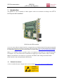
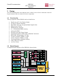
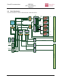
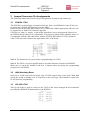
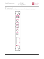
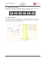
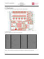
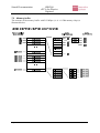
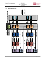
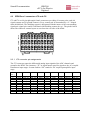
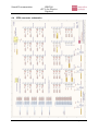
SIS Documentation
SIS8300
µTCA 16-bit Digitizer
SIS8300
µTCA FOR PHYSICS Digitizer
User Manual
SIS GmbH
Harksheider Str. 102A
22399 Hamburg
Germany
Phone: ++49 (0) 40 60 87 305 0
Fax:
++49 (0) 40 60 87 305 20
email: [email protected]
http://www.struck.de
Version: SIS8300-M-0201-001-V200.doc as of 28.06.11
Page 1 of 45
SIS Documentation
SIS8300
uTCA for Physics
Digitizer
Revision Table:
Revision
0.01
0.02
0.03
0.04
0.05
0.06
0.07
1.00
1.01
1.02
1.03
2.00
Page 2 of 45
Date
21.06.10
18.08.10
25.08.10
27.08.10
17.09.10
18.09.10
06.10.10
08.10.10
22.10.10
19.10.10
17.03.11
28.06.11
Modification
Based on AG notes
Clock Distribution
Vendor Id./PCI Id.
Register inlays
Add registers
Front panel description
RTM connectors
DAC comment
V0103 Firmware Release
JTAG over PCIe Index entry
JTAG parallel load note
Changes with new PCB version V2
- changed DAC interface
- add FPGA CRC check register
RTM management chapter
SIS Documentation
SIS8300
µTCA 16-bit Digitizer
- Table of contents
1
2
3
4
5
6
7
8
9
Table of contents....................................................................................................................................... 3
Introduction .............................................................................................................................................. 5
1.1
Related documents............................................................................................................................. 5
Design ...................................................................................................................................................... 6
2.1
Functionality ..................................................................................................................................... 6
2.2
Block Diagram .................................................................................................................................. 6
2.3
Platform Management........................................................................................................................ 7
2.4
Clock Distribution ............................................................................................................................. 8
Jumper/Connector Pin Assignments........................................................................................................... 9
3.1
CON100 JTAG.................................................................................................................................. 9
3.2
J604 Watchdog Reset......................................................................................................................... 9
3.3
J32 AVR JTAG ................................................................................................................................. 9
LEDs ...................................................................................................................................................... 10
4.1
AMC LEDs ..................................................................................................................................... 10
4.2
Front Panel LEDs ............................................................................................................................ 10
4.3
SMD LEDs...................................................................................................................................... 10
Front panel.............................................................................................................................................. 11
5.1
Harlink LVDS In-/Outputs............................................................................................................... 12
5.2
SMA Clock Input ........................................................................................................................... 12
Board Layout .......................................................................................................................................... 13
Firmware Description.............................................................................................................................. 14
7.1
Address Map ................................................................................................................................... 14
7.2
Memory buffer ................................................................................................................................ 16
7.3
ADC Sample Logic ......................................................................................................................... 17
7.4
Module Id. and Firmware Revision register...................................................................................... 18
7.5
Serial Number register ..................................................................................................................... 18
7.6
XILINX JTAG register .................................................................................................................... 19
7.7
XILINX Virtex5 Error Detection register ......................................................................................... 19
7.8
User Control/Status register ............................................................................................................ 20
7.9
ADC Acquisition Control/Status register......................................................................................... 21
7.10 ADC Sample Control register .......................................................................................................... 22
7.11 MLVDS Input/Output Control register............................................................................................. 23
7.12 Harlink Connector Input/Output Control register.............................................................................. 24
7.13 Clock Distribution Multiplexer control register ................................................................................ 25
7.13.1 Clock Multiplexer input signal assignments.............................................................................. 26
7.14 Clock Distribution AD9510 Serial Interface (SPI) interface register (0x41, read/write) ..................... 27
7.15 Clock Multiplier IC SI5326 SPI interface register............................................................................ 29
7.16 DAC Control register (0x45, read/write) .......................................................................................... 30
7.17 DAC Data register (0x46, read/write)............................................................................................... 30
7.18 ADC Serial Interface (SPI) interface register (0x48, read/write)........................................................ 31
7.19 ADC Input Tap delay registers (0x49).............................................................................................. 32
7.20 Virtex 5 System Monitor registers.................................................................................................... 32
7.21 Trigger setup register registers ......................................................................................................... 33
7.22 Trigger Threshold registers .............................................................................................................. 34
7.22.1 Trigger Threshold .................................................................................................................... 34
7.22.2 FIR Trigger Threshold.............................................................................................................. 35
7.23 Memory Sample Start Address / Actual Sample Address registers .................................................... 36
7.24 Sample Length register .................................................................................................................... 37
7.25 Ringbuffer Pretrigger Delay register................................................................................................. 37
RTM management................................................................................................................................... 38
Appendix ................................................................................................................................................ 39
9.1
Power Consumption......................................................................................................................... 39
9.2
Ordering options.............................................................................................................................. 39
9.3
RTM/Zone 3 connectors J75 and J76 ............................................................................................... 40
9.3.1
J75 connector pin assignments.................................................................................................. 40
9.3.2
J76 connector pin assignments.................................................................................................. 41
Page 3 of 45
SIS Documentation
SIS8300
uTCA for Physics
Digitizer
9.3.3
Note on AC/DC input stage selection........................................................................................ 41
9.4
RTM connector schematics.............................................................................................................. 43
10
Index................................................................................................................................................... 44
Page 4 of 45
SIS Documentation
1
SIS8300
µTCA 16-bit Digitizer
Introduction
The SIS8300 is a ten 10 channel 125 MS/s digitizer with 16-bit resolution according to the
for Physics draft standard.
uTCA
SIS8300 with SFPs installed
As we are aware, that no manual is perfect, we appreciate your feedback and will incorporate proposed
changes and corrections as quickly as possible. The most recent version of this manual can be obtained
by email from [email protected], the revision dates are online under http://www.struck.de/manuals.html .
Note 1: It is PICMG‘s policy to prohibit claims of compliance with respect to a specification under
development. Any such claims must be understood as applying to a draft, which is subject to change
Note 2: The SIS8300 is developed in co-operation with DESY under ZIM grant 2460101MS9
(ZIM: Zentrales Innovationsprogramm Mittelstand)
1.1 Related documents
A list of available firmware designs can be retrieved from http://www.struck.de/sis8300firm.html
Page 5 of 45
Struck Documentation
2
SIS8300
uTCA for Physics
Digitizer
Design
The central building block of the SIS8300 card is a Xilinx Virtex 5 FPGA. It holds the 4 lane PCI
Express interface and is in control of all active components.
2.1 Functionality
The key properties of the SIS8300 card are listed below.
Double size µTCA for Physics Board
4 Lane PCI Express Interface
Dual SFP Card Cage for optional Multi Gigabit Link
Xilinx Virtex 5 FPGA
DDR2 Memory Interface
4 x 1 GBit default DDR2 memory
Atmega128 IPMI
External Clock and Trigger Inputs
Frontpanel digital I/O (4in/4 out) on Harlink Connectors
RTM ADC Analog Inputs, I2C-Bus
10 ADC Channels 125MS/s, 16-Bit
2 DAC Channels 250MS/s, 16-Bit
Clock distribution with phase shifting
4 M-LVDS µTCA Ports
2 µTCA Clocks
2.2 Block Diagram
A simplified block diagram of the SIS8300 is shown below.
Page 6 of 45
Struck Documentation
2.3
SIS8300
uTCA for Physics
Digitizer
Platform Management
The management code of the SIS8300 is implemented in an Atmel Atmega1281-16MU
microcontroller and can be upgrade in field over connector J32 (see section 3.3).
Page 7 of 45
Struck Documentation
SIS8300
uTCA for Physics
Digitizer
2.4 Clock Distribution
The clock distribution scheme of the SIS8300 is illustrated below.
#2
2
0
MUX C
1
MUX E
1
3
3
2
0
ADCLK925
ADCLK925
MUX A
MUX B
1
2
0
3
1
2
Ch9
T
ADC
ADC
T
FPGA
CLK05
ADC
ADC
T
T
#1
3
ADC
ADC
µRTM
SI5324
AD9510
0
1
FPGA
CLK69
AD9510
MUX D
3
2
ADC
ADC
ADC
ADC
Ch1
Ch0
0
RTM_CLK0
RTM_CLK2
CLK1
CLK2
Backplane
ADCLK925
ADCLK946
ADCLK925
ADCLK925
ADCLK946
EXTCLKB
HARLINK
ADCLK925
Quartz
EXTCLKA
SMA
RTM_CLK1
Page 8 of 45
Struck Documentation
SIS8300
uTCA for Physics
Digitizer
3 Jumper/Connector Pin Assignments
The following subsections describe the pin assignments of jumpers and connectors.
3.1 CON100 JTAG
The SIS8300’s on board logic can load its firmware from a serial PROM, via the JTAG port
on connector CON100, PCI Express or via the MMC.
Hardware like the XILINX HW-USB-JTAG in connection with the appropriate software will
be required for in field JTAG firmware upgrades.
CON100 is a 2mm (i.e. metric) 14 pin header that allows you to reprogram the firmware of
the SIS8300 board with a JTAG programmer. The pin out is shown in the schematic below. It
is compatible with the cable that comes with the XILINX HW-USB-II-G-JTAG platform
cable. CON100 can be found at the right bottom side of the board.
Note 1: The board has to be powered for reprogramming over JTAG
Note 2: The FPGA uses 8-bit parallel mode to load the firmware from the serial PROM.
Make sure to check the 'Parallel Load' box in Impact when specifying the programming
properties for the PROM.
3.2 J604 Watchdog Reset
J604 can be found next to the left upper edge of U500 (largest chip on the card). With J604
closed the boards watchdog reset is connected to the reset logic. J604 should be opened for
JTAG firmware programming.
3.3 J32 AVR JTAG
This 10-pin header is used to connect to the JTAG of the Atmel Atmega128 microcontroller
providing the IPMI/MCH functionality of the SIS8300.
Page 9 of 45
Struck Documentation
4
SIS8300
uTCA for Physics
Digitizer
LEDs
4.1 AMC LEDs
The AMC LEDs are implemented according to the standard.
4.2 Front Panel LEDs
The SIS8300 in Gigalink stuffing option has 4 green front panel LEDs.
LED name
A
U
L1
L2
Function in Gigalink design
PCI Express Access
User LED
PCIe Link up (Optical Link 1 up)
ADC Sampling active (Optical Link 2 up)
4.3 SMD LEDs
A number of surface mount red LEDs are on the SIS8300 to visualize part of the board status.
LED designator
D20A
D20B
D20C
D20D
D20E
D20F
D20G
D20H
D21D
D105A
D105B
D110A
D110B
Page 10 of 45
LED comment
S1
S2
S3
S4
S5
S6
S7
S8
READY
TX FAULT 1
RX LOS 1
TX FAULT 2
RX LOS 2
Function
Firmware dependent
Firmware dependent
Firmware dependent
Firmware dependent
Firmware dependent
Firmware dependent
Firmware dependent
Firmware dependent
FPGA ready
Link 1 transmitter fault
Link 1 receiver loss of signal
Link 2 transmitter fault
Link 2 receiver loss of signal
Struck Documentation
SIS8300
uTCA for Physics
Digitizer
5 Front panel
The SIS8300 is a µTCA for Physics board. A sketch of the front panel is shown below.
Page 11 of 45
Struck Documentation
SIS8300
uTCA for Physics
Digitizer
5.1 Harlink LVDS In-/Outputs
The Harlink LVDS Output and Input connectors have 5 signals each. The Clock signal to the
left hand side is marked with C and the other 4 signals are labelled with 1-4.
Top
Bottom
Clock
P
N
1
P
N
2
P
N
3
P
N
4
P
N
5.2 SMA Clock Input
The front panel SMA clock input is designed to accept a maximum peak to peak signal level
of 3V into 50 Ohms. The clock input signal is coupled to the internal logic via a capacitor.
The schematic of the input stage is shown below.
Page 12 of 45
Struck Documentation
SIS8300
uTCA for Physics
Digitizer
6 Board Layout
A print of the silk screen of the component side is shown below.
Connector types
The used connectors are listed in the table below.
Designator
CON100
CON200
CON301
CON302
CAGE105
J10
J32
J75
J76
J77
J209
J205
J604
Function
JTAG
Clock In
DAC 1 Out
DAC 2 Out
SFP Cage, 2 Ports
AdvancedMC
JTAG Atmega
RTM
RTM
RTM Keying
Trigger & Clock Out
Trigger & Clock In
Watchdog
Manufacturer
Molex
JYEBAO
JYEBAO
JYEBAO
TYCO
HARTING
SAMTEC
ERNI
ERNI
TYCO
HARTING
HARTING
SAMTEC
Part Number
87831-1420
SMA8400A1-9000
SMA8400A1-9000
SMA8400A1-9000
1761014-1
16211701301000
HTSW-105-26-G-D
ERmetZD-10x3P-FEM
ERmetZD-10x3P-FEM
(*)
27 21 121 8000
27 21 121 8000
HTSW-102-26-G-S
Note (*): The used Key may depend on the hardware configuration of the SIS8300
Page 13 of 45
Struck Documentation
SIS8300
uTCA for Physics
Digitizer
7 Firmware Description
7.1 Address Map
Following 32-bit addresses are implemented
Offset
0x000
0x001
0x002
0x003
Access
R
R
R/W
R
0x004
R/W
User Control/Status register (JK)
0x010
0x011
0x012
0x013
R/W
R/W
R/W
R/W
ADC Acquisition Control/Status register
ADC Sample Control register
MLVDS Input/Output Control register
Harlink Connector Input/Output Control register
0x014
0x015
0x016
0x017
R/W
R/W
R/W
R/W
free
free
free
free
0x40
0x41
0x42
R/W
R/W
R/W
Clock Distribution Multiplexer control register
Clock Distribution IC AD9510 SPI interface register
Clock Multiplier IC SI5326 SPI interface register
0x44
0x45
0x46
R/W
R/W
R/W
reserved
DAC Control register
DAC Data register
0x48
0x49
R/W
R/W
ADC SPI Interface register
ADC Input Tap delay register
0x90
0x91
0x92
R/W
R/W
R/W
VIRTEX5_SYSTEM_MONITOR_DATA register
VIRTEX5_SYSTEM_MONITOR_ADDR register
VIRTEX5_SYSTEM_MONITOR_CTRL register
0x100
0x101
..
0x109
R/W
R/W
ADC ch1 Trigger Setup register
ADC ch2 Trigger Setup register
R/W
ADC ch10 Trigger Setup register
0x110
0x111
..
0x119
R/W
R/W
ADC ch1 Trigger Threshold register
ADC ch2 Trigger Threshold register
R/W
ADC ch10 Trigger Threshold register
Page 14 of 45
Function
Module Identifier/Firmware Version register
Serial number register
XILINX JTAG register
XILINX Virtex5 configuration memory Error Detection register
Struck Documentation
SIS8300
uTCA for Physics
Digitizer
0x120
0x121
..
0x129
R/W
R/W
ADC ch1 Memory Sample Start Address / Actual Address register
ADC ch2 Memory Sample Start Address / Actual Address register
R/W
ADC ch10 Memory Sample Start Address / Actual Address register
0x12A
R/W
ADC chx Sample Length Register
0x12B
R/W
ADC chx Ringbuffer Pretrigger Delay (0 to 2046)
0x12C
0x12D
0x12E
0x12F
R/W
R/W
R/W
R/W
free
free
free
free
0x200
0x201
0x202
0x203
0x204
R/W
R/W
R/W
R/W
R/W
R/W
R/W
R/W
R/W
R/W
R/W
R/W
R/W
R/W
R/W
R/W
R/W
R/W
R/W
W
DMA_READ_DST_ADR_LO32
DMA_READ_DST_ADR_HI32
DMA_READ_SRC_ADR_LO32
DMA_READ_LEN
DMA_READ_CTRL
0x210
0x211
0x212
0x213
0x214
0x230
0x211
0x3ff
DMA_WRITE_SRC_ADR_LO32
DMA_WRITE_SRC_ADR_HI32
DMA_WRITE_DST_ADR_LO32
DMA_WRITE_LEN
DMA_WRITE_CTRL
MEMORY test Mode register
DMA_WRITE_SRC_ADR_HI32
Bit 0 = 1:
Master Reset (reset all registers)
Page 15 of 45
Struck Documentation
SIS8300
uTCA for Physics
Digitizer
7.2 Memory buffer
The structure of the memory buffer with 512 MByte (i.e. 4 x 1 GBit memory chips) is
illustrated below.
Page 16 of 45
Struck Documentation
7.3
SIS8300
uTCA for Physics
Digitizer
ADC Sample Logic
Page 17 of 45
Struck Documentation
7.4
SIS8300
uTCA for Physics
Digitizer
Module Id. and Firmware Revision register
#define SIS8300_IDENTIFIER_VERSION_REG
0x00
This register holds the module identifier (SIS8300) and the firmware version and revision.
BIT access Name
31-16 RO
Function
Module Identifier
0x8300
Firmware Version
1..255
Firmware Revision
1..255
FFFF0000
15-8 RO
0000FF00
7-0 RO
000000FF
Example: The initial version of the SIS8300 reads 0x83000101
7.5
Serial Number register
#define SIS8300_SERIAL_NUMBER_REG
0x01
This register holds the Serial Number of the module.
BIT access Name
31-16 RO
Function
reserved
FFFF0000
15-0 RO
0000FFFF
Page 18 of 45
Serial Number
1..65535
Struck Documentation
7.6
SIS8300
uTCA for Physics
Digitizer
XILINX JTAG register
#define SIS8300_XILINX_JTAG_REG
0x02
XILINX JTAG register
This register is used in the firmware upgrade process over PCIe only. A TCK is generated
upon a write cycle to this register.
Bit
31
30
...
4
3
2
1
0
write Function
none
...
...
none
none
none
TMS
TDI
read Function
TDO
1 x Shifted TDO
30 x Shifted TDO
The read register function operates as a shift register for TDO. The content of the read register
is shifted to the right by one bit with every positive edge of TCK and the status of TDO is
transferred to Bit 30. Bit 31 reflects the current value of TDO during a read access.
7.7
XILINX Virtex5 Error Detection register
#define SIS8300_XILINX_ECC_REG
0x03
XILINX Virtex5 configuration memory error detection register.
Bit
31
30
...
16
15
14
13
12
11
..
1
0
read Function
0
0
0
Frame ECC output indicating a valid SYNDROME value
0
CRC Error
ECC Error
SYNDROME: Status bit 11
SYNDROME: Status bit 1
SYNDROME: Status bit 0
Page 19 of 45
Struck Documentation
7.8
SIS8300
uTCA for Physics
Digitizer
User Control/Status register
#define SIS8300_USER_CONTROL_STATUS_REG
0x04
The control register is implemented as a selective J/K register, a specific function is enabled
by writing a 1 into the set/enable bit, the function is disabled by writing a 1 into the
clear/disable bit (which location is 16-bit higher in the register). An undefined toggle status
will result from setting both the enable and disable bits for a specific function at the same
time. The only function at this point in time is user LED on/off.
On read access the same register represents the status register.
Bit
31
30
29
28
27
26
25
24
23
22
21
20
19
18
17
16
15
14
13
12
11
10
9
8
7
6
5
4
3
2
1
0
write Function
Clear reserved 15 (*)
Clear reserved 14 (*)
Clear reserved 13 (*)
Clear reserved 12 (*)
Clear reserved 11 (*)
Clear reserved 10 (*)
Clear reserved 9 (*)
Clear reserved 8 (*)
Clear reserved 7 (*)
Clear reserved 6 (*)
Clear reserved 5 (*)
Clear reserved 4 (*)
Clear reserved 3 (*)
Clear reserved 2 (*)
Clear reserved 1 (*)
Switch off user LED (*)
Set reserved 15
Set reserved 14
Set reserved 13
Set reserved 12
Set reserved 11
Set reserved 10
Set reserved 9
Set reserved 8
Set reserved 7
Set reserved 6
Set reserved 5
Set reserved 4
Set reserved 3
Set reserved 2
Set reserved 1
Switch on user LED
(*) denotes power up default setting
Page 20 of 45
read Function
0
0
0
0
0
0
0
0
0
0
0
0
0
0
0
0
Status reserved 15
Status reserved 14
Status reserved 13
Status reserved 12
Status reserved 11
Status reserved 10
Status reserved 9
Status reserved 8
Status reserved 7
Status reserved 6
Status reserved 5
Status reserved 4
Status reserved 3
Status reserved 2
Status reserved 1
Status User LED (1=LED on, 0=LED off)
Struck Documentation
7.9
SIS8300
uTCA for Physics
Digitizer
ADC Acquisition Control/Status register
#define SIS8300_ACQUISITION_CONTROL_STATUS_REG
Bit
31
30
29
28
...
...
17
16
15
12
11
10
9
8
7
6
5
4
3
2
1
0
write
0x10
/* rd/wr D32 */
read
Status: DDR2 Memory OK
Status: internal Sample Buffer Not Empty
Status: internal Sample Logic Busy
‘1’ : Disable Sampling
(Reset Sample Logic)
‘1’ : Arm Sampling
(Start with next trigger)
‘1’ : Start Sampling immediately
(Arm and Start/Trigger)
Status: Arm for trigger
(Wait for trigger)
Status: Sampling Busy
The power up default value is 0x0
Page 21 of 45
Struck Documentation
SIS8300
uTCA for Physics
Digitizer
7.10 ADC Sample Control register
#define SIS8300_SAMPLE_CONTROL_REG
0x11
/* rd/wr D32 */
ADC channels can be disabled from storing data to memory by setting the corresponding
disable bit in this register.
Bit
31
30
29
28
...
...
17
16
15
12
11
10
9
8
7
6
5
4
3
2
1
0
write
Enable external Trigger
Enable internal Trigger
Disable Sampling Ch10
Disable Sampling Ch9
Disable Sampling Ch3
Disable Sampling Ch2
Disable Sampling Ch1
The power up default value is 0x0
Page 22 of 45
Struck Documentation
SIS8300
uTCA for Physics
Digitizer
7.11 MLVDS Input/Output Control register
#define SIS8300_MLVDS_IO_CONTROL_REG
Bit
31
30
..
25
24
23
22
...
17
16
15
14
...
9
8
7
6
...
1
0
0x12
/* rd/wr D32 */
Write
Enable LVDS Output Bit 7
Enable LVDS Output Bit 6
Read
Enable LVDS Output Bit 7
Enable LVDS Output Bit 6
Enable LVDS Output Bit 1
Enable LVDS Output Bit 0
LVDS Output Bit 7
LVDS Output Bit 6
Enable LVDS Output Bit 1
Enable LVDS Output Bit 0
LVDS Output Bit 7
LVDS Output Bit 6
LVDS Output Bit 1
LVDS Output Bit 0
LVDS Input 7 External Trigger Enable
LVDS Input 6 External Trigger Enable
LVDS Output Bit 1
LVDS Output Bit 0
LVDS Input 7 External Trigger Enable
LVDS Input 6 External Trigger Enable
LVDS Input 1 External Trigger Enable
LVDS Input 0 External Trigger Enable
LVDS Input 7 External Trigger falling edge
LVDS Input 6 External Trigger falling edge
LVDS Input 1 External Trigger Enable
LVDS Input 0 External Trigger Enable
LVDS Input Bit 7
LVDS Input Bit 6
LVDS Input 1 External Trigger falling edge LVDS Input Bit 1
LVDS Input 0 External Trigger falling edge LVDS Input Bit 0
Note: external trigger in signals are synchronized with the FPGA CLK05
Page 23 of 45
Struck Documentation
SIS8300
uTCA for Physics
Digitizer
7.12 Harlink Connector Input/Output Control register
#define SIS8300_HARLINK_IO_CONTROL_REG
Bit
31
30
..
21
20
19
18
17
16
15
14
13
12
11
10
9
8
7
6
5
4
3
2
1
0
0x13
/* rd/wr D32 */
Write
No function
No function
Read
0
0
No function
No function
Harlink Output 4
Harlink Output 3
Harlink Output 2
No function
Harlink Input 4 External Trigger falling edge
Harlink Input 3 External Trigger falling edge
Harlink Input 2 External Trigger falling edge
Harlink Input 1 External Trigger falling edge
Harlink Input 4 External Trigger Enable
Harlink Input 3 External Trigger Enable
Harlink Input 2 External Trigger Enable
Harlink Input 1 External Trigger Enable
No function
No function
No function
No function
No function
No function
No function
No function
0
0
Harlink Output 4
Harlink Output 3
Harlink Output 2
0
Harlink Input 4 External Trigger falling edge
Harlink Input 3 External Trigger falling edge
Harlink Input 2 External Trigger falling edge
Harlink Input 1 External Trigger falling edge
Harlink Input 4 External Trigger Enable
Harlink Input 3 External Trigger Enable
Harlink Input 2 External Trigger Enable
Harlink Input 1 External Trigger Enable
0
0
0
0
Harlink Input 4
Harlink Input 3
Harlink Input 2
Harlink Input 1
Harlink Connector Input(1) : external trigger In
Harlink Connector Output(1) : adc chx (or) trigger out
Note: external trigger in signals are synchronized with the FPGA CLK05
Page 24 of 45
Struck Documentation
SIS8300
uTCA for Physics
Digitizer
7.13 Clock Distribution Multiplexer control register
#define SIS8300_CLOCK_DISTRIBUTION_MUX_REG 0x40
The SIS8300 has 5 IDT ICS853S057 clock multiplexer chips, which are labelled A to E in the
clock distribution schematic in section 2.4. The multiplexer control register holds the two
select bits for the 5 multiplexer chips as shown in the table below.
The assignment of the inputs to the resources (i.e. clock inputs) is listed in subsection 7.13.1.
BIT access Name
31-12 R/W
Function
reserved
no
MUXE_SEL
Multiplexer E select bits
MUXD_SEL
Multiplexer D select bits
reserved
no
MUXC_SEL
Multiplexer C select bits
MUXB_SEL
Multiplexer B select bits
MUXA_SEL
Multiplexer A select bits
FFFFF000
11-10 R/W
00000C00
9-8 R/W
00000300
7-6 R/W
000000C0
5-4 R/W
00000030
3-2 R/W
0000000C
1-0 R/W
00000003
Page 25 of 45
Struck Documentation
SIS8300
uTCA for Physics
Digitizer
7.13.1 Clock Multiplexer input signal assignments
7.13.1.1
Multiplexer A Input Signals:
U222 - Sel0 and Sel1 (MUX1A_SEL) = Multiplexer A select lines
Sel1
0
0
1
1
Sel0
0
1
0
1
7.13.1.2
Selected Input - Net Name
RTMCLK_0
TCLKB_0
TCLKA_0
OSC_CLK0
Clock source Description
Clock 2 from µRTM card
Clock 2 (Telecom Clock B) from AMC Connector (Backplane)
Clock 1 (Telecom Clock A) from AMC Connector (Backplane)
Onboard Clock chip (250MHz)
Multiplexer B Input Signals:
U223 - Sel0 and Sel1 (MUX1B_SEL) = Multiplexer B select lines
Sel1
0
0
1
1
Sel0
0
1
0
1
7.13.1.3
Selected Input - Net Name
RTMCLK_1
TCLKB_1
TCLKA_1
OSC_CLK1
Clock source Description
Clock 2 from µRTM card
Clock 2 (Telecom Clock B) from AMC Connector (Backplane)
Clock 1 (Telecom Clock A) from AMC Connector (Backplane)
Onboard Clock chip (250MHz)
Multiplexer C Input Signals:
U240 - Sel0 and Sel1 (MUXAB_SEL) = Multiplexer C select lines
Sel1
0
0
1
1
Sel0
0
1
0
1
7.13.1.4
Selected Input - Net Name
EXT_CLKB0
EXT_CLKA0
MUXA_CLK1
MUXB_CLK1
Clock source Description
Clock from Harlink Connector “CI1-4 IN” (frontpanel)
Clock from SMA Connector “CLK IN” (frontpanel)
Multiplexer A Output Signal
Multiplexer B Output Signal
Multiplexer D Input Signals:
U250 - Sel0 and Sel1 (MUX2A_SEL) = Multiplexer D select lines
Sel1
0
0
1
1
Sel0
0
1
0
1
7.13.1.5
Selected Input - Net Name
MUXA_CLK0
MUL_CLK1
EXT_CLKB1
EXT_CLKA1
Clock source Description
Multiplexer A Output Signal
Clock Multiplier (U242) Output 2 Signal
Clock from Harlink Connector “CI1-4 IN” (frontpanel)
Clock from SMA Connector “CLK IN” (frontpanel)
Multiplexer E Input Signals:
U251 - Sel0 and Sel1 (MUX2B_SEL) = Multiplexer E select lines
Sel1
0
0
1
1
Sel0
0
1
0
1
Page 26 of 45
Selected Input - Net Name
MUXB_CLK0
MUL_CLK0
EXT_CLKB2
EXT_CLKA2
Clock source Description
Multiplexer B Output Signal
Clock Multiplier (U242) Output 1 Signal
Clock from Harlink Connector “CI1-4 IN” (frontpanel)
Clock from SMA Connector “CLK IN” (frontpanel)
Struck Documentation
SIS8300
uTCA for Physics
Digitizer
7.14 Clock Distribution AD9510 Serial Interface (SPI) interface register (0x41,
read/write)
#define SIS8300_AD9510_SPI_REG
x41
/* read/write; D32 */
The parameters of the Clock Distribution IC AD9510 chips can be configured with the SPI
(serial Peripheral Interface).
...
...
25
24
23
22
21
20
19
12
11
10
9
8
7
6
..
1
0
Write
Cmd Bit 1
Cmd Bit 0
Set “Function” Output Level
Select “Function”
synchronisation CLK
AD9510 #2 Select Bit
Read Cycle Bit
read
Write/Read Logic BUSY Flag
Status of Set “Function” Output Level
Status of Select “Function”
synchronisation CLK
Status AD9510 #2
Status AD9510 #1
Address Bit 12
Address Bit 11
RW CMD
Bit
31
30
29
28
Address Bit 4
Address Bit 3
Address Bit 2
Address Bit 1
Address Bit 0
Write Data Bit 7 (MSB)
Write Data Bit 6
Read Data Bit 7 (MSB)
Read Data Bit 6
Write Data Bit 1
Write Data Bit 0 (LSB)
Read Data Bit 1
Read Data Bit 0 (LSB)
The power up default value is 0x20000000
Page 27 of 45
Struck Documentation
SIS8300
uTCA for Physics
Digitizer
Command Bit (31:30) Explanation:
Cmd Bit 1
0
0
1
Cmd Bit 0
0
1
0
1
1
Command
No Function
R/W CMD
Function CMD
Generates a pulse at the Function Input pin of the AD9510
which is synchronous to the selected clock. The clock
selection is done via Bit 28 (Function Syn CLK).
The actual function depends on the programming of the
selected AD9510
Reserved
Select “Function” synchronisation CLK Bit (28) Explanation:
Bit 28
0
1
Clock Source
PCI Clock
FPGA CLK 69
Note:
1. enable READ by writing 0x90 to addr 0x0
2. and set Read Cycle Bit
Note:
Please refer to the SIS8300_AD9510_SPI_Setup routine as illustration and to the AD9510
documentation for details.
Page 28 of 45
Struck Documentation
SIS8300
uTCA for Physics
Digitizer
7.15 Clock Multiplier IC SI5326 SPI interface register
#define SIS8300_CLOCK_MULTIPLIER_SPI_REG
x42 /* rd/wr */
Clock Multiplier IC SI5326 SPI interface register
Several parameters of the Clock Multiplier SI5326 chip can be configured with the SPI
(serial Peripheral Interface).
Please refer to the documentation of the SI5326chip for details.
Bit
31
30
29
...
17
16
15
..
..
8
7
..
..
0
Write
Cmd Bit 1
Cmd Bit 0
read
Write/Read Logic BUSY Flag
Reset, Decrement or Increment Cmd BUSY Flag
Si53xx LOL Status
Si53xx INT_C1B Status
Instruction Byte Bit 7
Instruction Byte Bit 0
Address/Data Byte Bit 7
Read Data Bit 7 (MSB)
..
Address/Data Byte Bit 0
Read Data Bit 1
Read Data Bit 0 (LSB)
The power up default value is 0x0
Cmd Bit 1
0
0
1
1
Cmd Bit 0
0
1
0
1
Command
Execute SPI Write/Read Cmd
Reset Cmd
Decrement Cmd
Increment Cmd
Reset Cmd:
generates an 1us reset pulse
Decrement Cmd:
Increment Cmd:
generates an 1us Skew Decrement pulse
generates an 1us Skew Increment pulse
Note: INC/DEC Time between consecutive pulses must be greater than 16ms !
Page 29 of 45
Struck Documentation
SIS8300
uTCA for Physics
Digitizer
7.16 DAC Control register (0x45, read/write)
#define SIS8300_DAC_CONTROL_REG
Bit
31
...
16
15
…
12
11
10
9
8
7
6
5
4
..
1
0
0x45
write
/* read/write; D32 */
read
DAC DCM Reset pulse
0: binary, 1: 2-er complement
Test Mode Bit 1
Test Mode Bit 0
The power up default value is 0x0
Test Mode Bit 1
0
0
1
1
Test Mode Bit 0
0
1
0
1
DAC Test Mode
Data from DAC Data register
Ramp Test Mode
ADC1/ADC2 -> DAC1/DAC2
reserved
Note: ADC 1 Clock is used as DAC clock
7.17 DAC Data register (0x46, read/write)
#define SIS8300_DAC_DATA_REG
Bit
31
...
...
16
15
...
...
0
write
DAC2 Data 15
DAC2 Data 0
DAC1 Data 15
DAC1 Data 0
The power up default value is 0x0
Page 30 of 45
0x46
/* read/write; D32 */
Struck Documentation
SIS8300
uTCA for Physics
Digitizer
7.18 ADC Serial Interface (SPI) interface register (0x48, read/write)
#define SIS8300_ADC_SERIAL_INTERFACE_REG
0x48
/* read/write; D32 */
Several parameters of the ADC AD9268 chip can be configured with the SPI (serial
Peripheral Interface).
Please refer to the documentation of the ADC AD9268 chip for details.
Bit
31
...
...
26
25
24
23
22
21
20
19
write
ADC Synch cmd
read
Write/Read Logic BUSY Flag
12
11
10
9
8
7
6
..
1
0
Address Bit 4
Address Bit 3
Address Bit 2
Address Bit 1
Address Bit 0
Write Data Bit 7 (MSB)
Write Data Bit 6
Read Data Bit 7 (MSB)
Read Data Bit 6
Write Data Bit 1
Write Data Bit 0 (LSB)
Read Data Bit 1
Read Data Bit 0 (LSB)
ADC Select Mux Bit 2
ADC Select Mux Bit 1
ADC Select Mux Bit 0
Read Cmd
Address Bit 12
Address Bit 11
The power up default value is 0x0
ADC Synch Cmd : generates an synch pulse with AD9510 #1 FPGA clock
Page 31 of 45
Struck Documentation
SIS8300
uTCA for Physics
Digitizer
7.19 ADC Input Tap delay registers (0x49)
#define SIS3305_ADC_INPUT_TAP_DELAY
0x49
The input tap delay registers are used to adjust the FPGA data strobe timing.
Bit
Function
Bit
31
...
..
..
12
11
10
9
8
7
6
..
1
0
31-13 12
11
None ADC 9/10 ADC 7/8
Select
Select
10
ADC 5/6
Select
write
9
ADC 3/4
Select
8
ADC 1/2
Select
7-6
5-0
None Tap delay value
( x 78ps)
read
Tap Delay Logic BUSY Flag
ADC 9/10 Select Bit
ADC 7/8 Select Bit
ADC 5/6 Select Bit
ADC 3/4 Select Bit
ADC 1/2 Select Bit
Tap delay value Bit 7
Tap delay value Bit 6
Tap delay value Bit 7
Tap delay value Bit 6
Tap delay value Bit 1
Tap delay value Bit 0
Tap delay value Bit 1
Tap delay value Bit 0
7.20 Virtex 5 System Monitor registers
#define SIS8300_VIRTEX5_SYSTEM_MONITOR_DATA_REG
#define SIS8300_VIRTEX5_SYSTEM_MONITOR_ADDR_REG
#define SIS8300_VIRTEX5_SYSTEM_MONITOR_CTRL_REG
The Virtex 5 system monitor registers
voltages of the FPGA on the SIS8300.
give
0x90
0x91
0x92
access
to
temperature
Refer to the sysmon.c routine and the Virtex 5 FPGA documentation for details.
Page 32 of 45
and
Struck Documentation
SIS8300
uTCA for Physics
Digitizer
7.21 Trigger setup register registers
#define SIS8300_TRIGGER_SETUP_CH1_REG
0x100
/* rd/wr D32 */
0x109
/* rd/wr D32 */
..
#define SIS8300_TRIGGER_SETUP_CH10_REG
These read/write registers hold the 8-bit wide trigger pulse length (in sample clocks),
the Peaking and Gap Time of the trapezoidal FIR filter.
(Gap Time = SumG Time – Peaking Time)
Bit
Function
31
Reserved
..
..
26
Enable Trigger
25
GT trigger condition
24
FIR Trigger Mode
23
Puls Length bit 7
22
Puls Length bit 6
21
Puls Length bit 5
20
Puls Length bit 4
19
Puls Length bit 3
18
Puls Length bit 2
17
Puls Length bit 1
16
Puls Length bit 0
15
reserved
14
reserved
13
reserved
12
SumG bit 4
11
SumG bit 3
10
SumG bit 2
9
SumG bit 1
8
SumG bit 0
7
reserved
6
reserved
5
reserved
4
P bit 4
3
P bit 3
2
P bit 2
1
P bit 1
0
P bit 0
The power up default value reads 0x 00000000
Trigger Pulse Length
SumG time (only FIR trigger)
(time between both sums)
Peaking time P (only FIR trigger)
x+P
Si
i=x
Si:
Sum of ADC input sample stream from x to x+P
P:
Peaking time (number of values to sum)
SumG: SumGap time (distance in clock ticks of the two running sums)
The maximum SumG time:
The minimun SumG time:
Values > 16 will be set to 16
Value = 0 will be set to 1
16 (clocks)
1 (clocks)
The maximum Peaking time:
The minimun Peaking time:
Values > 16 will be set to 16
Value = 0 will be set to 1
16 (clocks)
1 (clocks)
Page 33 of 45
Struck Documentation
SIS8300
uTCA for Physics
Digitizer
7.22 Trigger Threshold registers
#define SIS8300_TRIGGER_THRESHOLD_CH1_REG
0x110
/* rd/wr D32 */
0x119
/* rd/wr D32 */
..
#define SIS8300_TRIGGER_THRESHOLD_CH10_REG
These read/write registers hold the threshold values for the 10 ADC channels.
7.22.1 Trigger Threshold
Bit
Function
31-16
Threshold value OFF
default after Reset:
15-0
Threshold value ON
0x0
A trigger output pulse is generated on two conditions:
GT is set (GT) in trigger setup register:
the trigger Out pulse will be issued if the actual sampled ADC value goes above the
threshold value ON and OFF. A new Trigger Out Pulse will be suppressed until the
ADC value goes below the threshold value OFF.
GT is cleared (LT) in trigger setup register:
the trigger Out pulse will be issued if the actual sampled ADC value goes below the
threshold value ON and OFF. A new trigger Out pulse will be suppressed until the ADC
value goes above the threshold value OFF.
the trigger Out pulse will be issued if the actual sampled ADC value goes below the
threshold value.
GT: greater than
LT: lower than
Page 34 of 45
Struck Documentation
SIS8300
uTCA for Physics
Digitizer
7.22.2 FIR Trigger Threshold
Bit
Function
31-20
None
default after Reset:
19-0
Trapezoidal threshold value
0x0
The value of the Sum (trapezoidal value) depends on the peaking time P. Therefore the
selection of the value of the Trapezoidal threshold depends on P also.
Trapezoidal value calculation:
Trapezoidal value = (SUM2 – SUM1)
Where
x+P
Si
SUM1 =
i=x
x+P+sumG
SUM2 =
Sj
j = x+sumG
The FIR filter logic generates the Trapezoidal by subtraction of the two running sums.
This implies, that the internal value of the trapezoid is on average 0.
A trigger output pulse is generated:
GT is set (GT):
the Trigger Out Pulse will be issued if the actual trapezoidal value goes above the
programmable trapezoidal threshold value
GT is cleared (LT):
the Trigger Out Pulse will be issued if the actual trapezoidal value goes below the
negated programmable trapezoidal threshold value
Page 35 of 45
Struck Documentation
SIS8300
uTCA for Physics
Digitizer
7.23 Memory Sample Start Address / Actual Sample Address registers
#define SIS8300_SAMPLE_START_ADDRESS_CH1_REG
..
#define SIS8300_SAMPLE_START_ADDRESS_CH10_REG
0x120 /* rd/wr D32 */
0x129 /* rd/wr D32 */
The write function to these registers defines the memory start address.
The value is given in 256-bit blocks.
ADC ch1 Memory Sample Start Address / Actual Address register
Bit
31-24
23-0
Write
reserved
Memory Sample Start Address (256-bit blocks)
Function
(16-bit word address x 16)
default after Reset: 0x0
The power up default value is 0
Explanation (memory sample start address)
The contents of the sample memory start address register is assigned as memory data
storage address with the arm command (key address arm sampling) or with the enable
command (key address enable sampling).
The read function from these registers give the information of the actual sampling address for
the given ADC channel.
(at the moment: only valid if the logic is not busy!)
The value is given in 256-bit Blocks (16bit word address x 16)
Bit
Read
Function
31-24
reserved
23-0
Actual Sample Memory Address (in 256-bit Blocks)
(16-bit word address x 16)
the power up default value is 0
Page 36 of 45
Struck Documentation
SIS8300
uTCA for Physics
Digitizer
7.24 Sample Length register
#define SIS8300_SAMPLE_LENGTH_REG
0x12A /* rd/wr D32 */
This register defines the number of sample blocks of each ADC Event or.
The size of one sample block for each ADC channel is 256-bit (16 x 16-bit word).
Bit
Function
31-24
reserved
default after Reset:
7-0
Sample Block Length
0x0
7.25 Ringbuffer Pretrigger Delay register
#define SIS8300_PRETRIGGER_DELAY_REG
0x12B /* rd/wr D32 */
This register defines the number of pre trigger delay samples for all channels.
The maximum pre trigger delay value is 2046.
Bit
Function
31-26
reserved
10-0
Delay value
Page 37 of 45
Struck Documentation
SIS8300
uTCA for Physics
Digitizer
8 RTM management
Connected RTMs shall be compliant to the PICMG MTCA.4 specification in a way that they
must have an on board I²C EEProm (on address 0x50) and a NXP PCF8574-compatible port
expander (on address 0x7C).
Required port expander connection map for normal operation:
Port pin
P0
P1
P2
P3
P4
P5
P6
P7
Function
HotSwap Switch (low active)
LED Blue (low active)
LED Red (low active)
LED Green (low active)
PowerGood (low active)
Reset (low active)
PowerEnable (low active)
EEprom Write Protect
The EEprom shall contain any relevant device information (FRU records) about the RTM
(refer to PICMG AMC.0). Additionally the EEprom shall contain the new record types
defined in PICMG MTCA.4.
In order to be able to decide whether a connected RTM is compatible to the SIS8300 the
RTM record shall contain one of the Zone 3 Identifier records listed in the table below.
Supported Zone 3 Identifier Records (Interface Identifier OEM):
IANA PEN (Private
enterprise number)
0x0092BD (37565)
Zone 3 OEM record
Descripton
0x83000001
0x00053F (1343)
0x08020000
SIS8300 Zone3 - v1
compatibility
DESY DWC Zone3
compatibility
Page 38 of 45
Struck Documentation
SIS8300
uTCA for Physics
Digitizer
9 Appendix
9.1 Power Consumption
The currents drawn by the SIS8300 are listed in the table below.
Voltage
3,3 V
12 V
Current
100 mA
2A
These currents are typical values during normal operation. They can vary depending on the
loaded firmware design.
9.2 Ordering options
The available part numbers are listed in the table below.
Struck part number
04075
To be defined
FPGA
SIS8300 V2 with XC5VLX50T-3FFG1136C
XC5VLX110T-1/3FFG1136C
Memory
4 x 1 GBit
5 x 1 GBit
Note: The V1 and V2 preseries cards are stuffed with the fastest available speed grade -3. A
lower speed grade -1 version may be desirable for high volume applications when speed
considerations are not an issue.
Page 39 of 45
Struck Documentation
SIS8300
uTCA for Physics
Digitizer
9.3 RTM/Zone 3 connectors J75 and J76
J75 and J76 are 90 pin right angle female connectors providing 30 contact pairs each (60
signal contacts and 30 ground contacts). Every contact pair is surrounded by a “L” shaped
male shield blade. The shielding contact is designated with the names of the corresponding
signal pair (signal pin a and b is affiliated with shielding contact ab e.g.). The picture below
shows the connector contact layout as seen from the rear side of the board.
9.3.1 J75 connector pin assignments
The J75 connector routes the differential analog input signals of the ADC channels and
ground to the RTM. The characters “TF” in signal names stand for signals to the AC coupled
transformer input stages. In same fashion “PA” stands for DC coupled preamplifier input
stage.
Col
Row
10
9
8
7
6
5
4
3
2
1
ef
f
e
cd
d
c
ab
b
a
GND
GND
GND
GND
GND
GND
GND
GND
GND
GND
CH9_PACH1_TFCH7_PACH3_TFCH5_PACH5_TFCH3_PACH7_TFCH1_PACH9_TF-
CH9_PA+
CH1_TF+
CH7_PA+
CH3_TF+
CH5_PA+
CH5_TF+
CH3_PA+
CH7_TF+
CH1_PA+
CH9_TF+
GND
GND
GND
GND
GND
GND
GND
GND
GND
GND
GND
GND
GND
GND
GND
GND
GND
GND
GND
GND
GND
GND
GND
GND
GND
GND
GND
GND
GND
GND
GND
GND
GND
GND
GND
GND
GND
GND
GND
GND
CH0_TFCH8_PACH2_TFCH6_PACH4_TFCH4_PACH6_TFCH2_PACH8_TFCH0_PA-
CH0_TF+
CH8_PA+
CH2_TF+
CH6_PA+
CH4_TF+
CH4_PA+
CH6_TF+
CH2_PA+
CH8_TF+
CH0_PA+
Page 40 of 45
Struck Documentation
SIS8300
uTCA for Physics
Digitizer
9.3.2 J76 connector pin assignments
The J76 connector is used to route power, data and system management pins to the RTM
board.
Col
Row
10
9
8
7
6
5
4
3
2
1
ef
f
e
Cd
d
c
ab
b
a
GND
GND
GND
GND
GND
GND
GND
GND
GND
GND
GND
CLK1GND
GND
D11D8D5D2SCL_I
SDA_I
GND
CLK1+
GND
GND
D11+
D8+
D5+
D2+
SCL_E
SDA_E
GND
GND
GND
GND
GND
GND
GND
GND
GND
GND
GND
GND
CLK2GND
D10D7D4D1SCL
SDA
GND
GND
CLK2+
GND
D10+
D7+
D4+
D1+
MP+3.3V
PS#
GND
GND
GND
GND
GND
GND
GND
GND
GND
GND
GND
CLK0GND
GND
D9D6D3D0PWR+12V
PWR+12V
GND
CLK0+
GND
GND
D9+
D6+
D3+
D0+
PWR+12V
PWR+12V
9.3.3 Note on AC/DC input stage selection
The AC (transformer) or DC (operation amplifier Opamp) input path is selected on the
SIS8300 card via 0603 solder bridges as illustrated for channels 0 and 1 on the screenshot
below. The designators for all channels can be found in the table below.
Page 41 of 45
Struck Documentation
SIS8300
uTCA for Physics
Digitizer
xxx
ADC Channel
0
0
1
1
2
2
3
3
4
4
5
5
6
6
7
7
8
8
9
9
Page 42 of 45
Designator
SW63A
SW63B
SW61A
SW61B
SW58A
SW58B
SW56A
SW56B
SW53A
SW53B
SW51A
SW51B
SW48A
SW48B
SW46A
SW46B
SW43A
SW43B
SW41A
SW41B
Input for ADC
ADC_CH0+
ADC_CH0ADC_CH1+
ADC_CH1ADC_CH2+
ADC_CH2ADC_CH3+
ADC_CH3ADC_CH4+
ADC_CH4ADC_CH5+
ADC_CH5ADC_CH6+
ADC_CH6ADC_CH7+
ADC_CH7ADC_CH8+
ADC_CH8ADC_CH9+
ADC_CH9-
Struck Documentation
SIS8300
uTCA for Physics
Digitizer
9.4 RTM connector schematics
Page 43 of 45
Struck Documentation
SIS8300
uTCA for Physics
Digitizer
10 Index
12 V 39
3,3 V 39
8-bit 9
A 10
AC 41
AD9268 31
AD9510 27
ADC Sample Logic 17
Address Map 14
AdvancedMC 6
AMC 6
AMC.0 38
Appendix 39
arm 36
Atmega 13
Atmega128 9
Atmel 7, 9
AVR JTAG 9
Block diagram 6
board layout 13
clock
input 12
clock distribution 8
clock multiplexer input signal assignments 26
CON600 9
connector types 13
CRC 19
DAC 13
DC 41
design 6
DESY 5
ECC 19
ERNI 13
firmware
version 18
Firmware 14
FPGA 6
front panel 11
FRU 38
functionality 6
Harlink 12
HARTING 13
IANA 38
IANA PEN 38
ICS853S057 25
IDT 25
impact 9
introduction 5
IPMI 7, 9
J32 7, 9
J604 9
J75 40, 41
JTAG 9, 13, 14
AVR 9
over PCIe 19
register 19
jumper 9
JYEBAO 13
L1 10
L2 10
LED 10
20A 10
Page 44 of 45
A 10
D105A 10
D105B 10
D110A 10
D110B 10
D20B 10
D20C 10
D20D 10
D20E 10
D20F 10
D20G 10
D20H 10
D21D 10
L1 10
L2 10
U 10
user 20
LEDs
AMC 10
Front Panel 10
SMD 10
LVDS 12
M 33
MCH 9
memory buffer 16
microcontroller 7, 9
MOLEX 13
MTCA.4 38
multiplexer A 26
multiplexer B 26
multiplexer C 26
multiplexer D 26
multiplexer E 26
NXP 38
ordering options 39
P 33
parallel load 9
PCF8574 38
PCI Express 6
PEN 38
PICMG 5
platform management 7
Power Consumption 39
register
ADC Acquisition Control/Status 21
ADC IOB delay 32
ADC Sample Control 22
ADC serial interface 31
clock distribution AD9510 SPI interface 27
clock distribution multiplexer control 25
Clock Multiplier IC SI5326 SPI interface 29
control 18
DAC control 30
DAC Data 30
firmware revision 18
Harlink Connector Input/Output Control 24
Memory Sample Start Address 36
MLVDS Input/Output Control 23
module Id. 18
ringbuffer pretrigger delay 37
Sample Length 37
serial number 18
Struck Documentation
trigger setup 33, 34
trigger threshold 34
User Control/Status 20
XILINX JTAG 19
XILINX Virtex5 Error Detection 19
registers
Virtex 5 System Monitor 32
RTM 38
RTM connector schematics 43
RTM connectors 40
RTM management 38
SAMTEC 13
SFP 6, 13
SI5326 29
SIS8300 5
SMA 12
SYNDROME 19
TDI 19
TDO 19
temperature 32
TMS 19
SIS8300
uTCA for Physics
Digitizer
trigger threshold 34
TYCO 13
U 10
U222 26
U223 26
U240 26
U250 26
U251 26
U500 9
user
LED 20
Virtex 5 6
Virtex5 Error Detection
register 19
watchdog reset 9
XC5VLX110T-1FFG1136C 39
XC5VLX50T-3FFG1136C 39
Xilinx 6
ZIM 5
Zone 3 40
Page 45 of 45