1
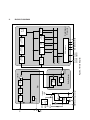
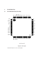
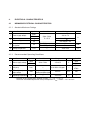
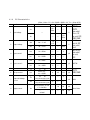
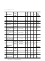
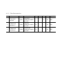
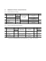
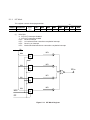
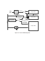
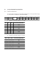
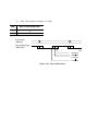
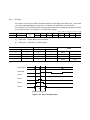
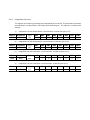
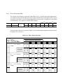
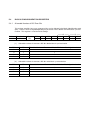
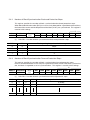
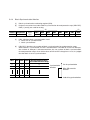
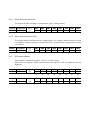
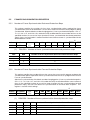
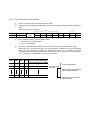
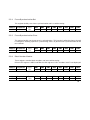
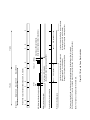
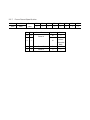
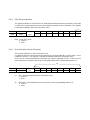
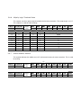
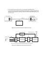
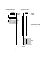
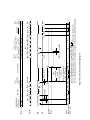
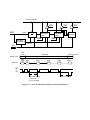
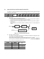
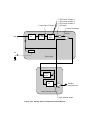
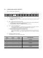
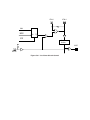
查询MSM9552供应商
捷多邦,专业PCB打样工厂,24小时加急
出货
¡
MSM9552/9553
IC for FM Multiplex
Broadcast Reception
User's Manual
Ver. 1.0
ISSUE DATE: Mar., 1998
IMPORTANT NOTICE
DARC (DAta Radio Channel), an FM multiplex broadcast technology, has been developed by
NHK (Japan Broadcasting Corporation). DARC is a registered trademark of NHK Engineering
Service (NHK-ES).
Any manufacturer who intends to manufacture/sell products that utilize DARC technology needs
to be licensed by NHK-ES.
For detailed information on licenses, please contact:
NHK Engineering Service
Phone: (+81) 3-3417-4840
E2Y0001-28-30
NOTICE
1.
The information contained herein can change without notice owing to product and/or
technical improvements. Before using the product, please make sure that the information
being referred to is up-to-date.
2.
The outline of action and examples for application circuits described herein have been
chosen as an explanation for the standard action and performance of the product. When
planning to use the product, please ensure that the external conditions are reflected in the
actual circuit, assembly, and program designs.
3.
When designing your product, please use our product below the specified maximum
ratings and within the specified operating ranges including, but not limited to, operating
voltage, power dissipation, and operating temperature.
4.
Oki assumes no responsibility or liability whatsoever for any failure or unusual or
unexpected operation resulting from misuse, neglect, improper installation, repair, alteration
or accident, improper handling, or unusual physical or electrical stress including, but not
limited to, exposure to parameters beyond the specified maximum ratings or operation
outside the specified operating range.
5.
Neither indemnity against nor license of a third party's industrial and intellectual property
right, etc. is granted by us in connection with the use of the product and/or the information
and drawings contained herein. No responsibility is assumed by us for any infringement
of a third party's right which may result from the use thereof.
6.
The products listed in this document are intended for use in general electronics equipment
for commercial applications (e.g., office automation, communication equipment,
measurement equipment, consumer electronics, etc.). These products are not authorized
for use in any system or application that requires special or enhanced quality and reliability
characteristics nor in any system or application where the failure of such system or
application may result in the loss or damage of property, or death or injury to humans.
Such applications include, but are not limited to, traffic and automotive equipment, safety
devices, aerospace equipment, nuclear power control, medical, and life-support systems.
7.
Certain products in this document may need government approval before they can be
exported to particular countries. The purchaser assumes the responsibility of determining
the legality of export of these products and will take appropriate and necessary steps at their
own expense for these.
8.
No part of the contents cotained herein may be reprinted or reproduced without our prior
permission.
9.
MS-DOS is a registered trademark of Microsoft Corporation.
Copyright 1998 Oki Electric Industry Co., Ltd.
Printed in Japan
TABLE OF CONTENTS
1. GENERAL DESCRIPTION .....................................................................................1-1
2. BLOCK DIAGRAM
.............................................................................................2-1
3. PIN INFORMATION .............................................................................................3-1
3.1 PIN CONFIGURATION (TOP VIEW) ..............................................................3-1
3.2 PIN DESCRIPTIONS .....................................................................................3-2
4. ELECTRICAL CHARACTERISTICS .......................................................................4-1
4.1 MSM9552 ELECTRICAL CHARACTERISTICS ............................................. 4-1
4.1.1 Absolute Maximum Ratings ...............................................................4-1
4.1.2 Recommended Operating Conditions ...............................................4-1
4.1.3 DC Characteristics .............................................................................4-2
4.1.4 AC Characteristics .............................................................................4-3
4.1.5 Filter Characteristics ..........................................................................4-4
4.2 MSM9553 ELECTRICAL CHARACTERISTICS ............................................. 4-5
4.2.1 Absolute Maximum Ratings ...............................................................4-5
4.2.2 Recommended Operating Conditions ...............................................4-5
4.2.3 DC Characteristics .............................................................................4-6
4.2.4 AC Characteristics .............................................................................4-7
4.2.5 Filter Characteristics ..........................................................................4-8
4.3 TIMING DIAGRAM ........................................................................................4-9
5. CONTROL REGISTERS ........................................................................................5-1
5.1 INTERRUPT REGISTERS ..............................................................................5-1
5.1.1 Interrupt Source .................................................................................5-1
5.1.2 INT Mask ............................................................................................5-3
5.2 RECEIVE DATA REGISTERS ........................................................................5-4
5.2.1 Receive Block Status ......................................................................... 5-4
5.2.2 Receive Data RAM Port .....................................................................5-6
5.2.3 Receive RAM, Data Accumulation Condition, and Address Clear .... 5-6
5.2.4 BIC Monitor .......................................................................................5-7
5.3 CLOCK REGENERATION REGISTERS......................................................... 5-10
5.3.1 Fixed Phase Adjustment .................................................................... 5-10
5.3.2 Bit Gate ..............................................................................................5-12
5.3.3 Integration Constant ..........................................................................5-13
5.3.4 Phase Correction Step ......................................................................5-14
5.4 BLOCK SYNCHRONIZATION REGISTERS .................................................. 5-15
5.4.1 Allowable Number of BIC Error Bits .................................................. 5-15
5.4.2 Number of Block Synchronization Backward Protection Steps ........5-16
5.4.3 Number of Block Synchronization Forward Protection Steps ........... 5-16
5.4.4 Block Synchronization Monitor ..........................................................5-17
5.4.5 Block Synchronization Set .................................................................5-18
5.4.6 Block Synchronization Clear ..............................................................5-18
5.4.7 Bit Number Monitor ........................................................................... 5-18
5.5 FRAME SYNCHRONIZATION REGISTERS .................................................. 5-19
5.5.1 Number of Frame Synchronization Backward Protection Steps ....... 5-19
5.5.2 Number of Frame Synchronization Forward Protection Steps .......... 5-19
5.5.3 Frame Synchronization Monitor......................................................... 5-20
5.5.4 Frame Synchronization Set................................................................ 5-21
5.5.5 Frame Synchronization Clear ............................................................5-21
5.5.6 Block Number Monitor ......................................................................5-21
5.5.7 Frame Format Specification ..............................................................5-23
5.6 ERROR CORRECTION REGISTERS ............................................................. 5-24
5.6.1 Internal Memory Address Counter Clear ........................................... 5-24
5.6.2 Data Transfer Port for Error Correction ............................................. 5-24
5.6.3 Error Correction Start Signal ............................................................. 5-25
5.6.4 CRC Result Indication .......................................................................5-26
5.6.5 Error Correction Result Indication .....................................................5-26
5.6.6 Majority Logic Threshold Value ......................................................... 5-27
5.6.7 Internal Address Monitor ...................................................................5-27
5.7 LAYER 4 CRC REGISTERS ..........................................................................5-31
5.7.1 Layer 4 CRC Register Clear ...............................................................5-31
5.7.2 Layer 4 CRC Data Buffer ...................................................................5-31
5.7.3 Layer 4 CRC Result Indication........................................................... 5-31
5.7.4 Layer 4 CRC Register ........................................................................5-32
5.8 ANALOG SECTION CONTROL/MONITOR REGISTER ................................ 5-34
5.9 POWER DOWN CONTROL REGISTER ........................................................5-37
5.10 TEST CONTROL REGISTERS .......................................................................5-39
5.10.1 Test Control 0 .................................................................................... 5-39
5.10.2 Test Control 1 .................................................................................... 5-39
5.11 I/O ADDRESS REGISTER .............................................................................5-42
5.12 EXTENDED PORT REGISTER .......................................................................5-43
6. EXTERNAL CONNECTION EXAMPLE .................................................................. 6-1
7. APPLICATION CIRCUIT ........................................................................................7-1
APPENDIX: INTERNATIONAL FRAME FORMAT ....................................................... Appendix-1
Chapter 1
GENERAL DESCRIPTION
1.
GENERAL DESCRIPTION
The MSM9552 and MSM9553 are LSI devices which demodulate FM character multiplex signals
in the DARC (DAta Radio Channel) format to acquire digital data. These devices operate on 5 V
and 3 V, respectively. In the DARC format, baseband signals at ordinary FM broadcasting
frequencies are multiplexed with 16 kbps digital data which are L-MSK-modulated at 76 kHz.
Each device has a bandpass filter consisting of SCF, frame synchronization circuit, and error
correction circuit, on a single chip.
They allow a system for acquisition of digital data to be easily constructed by externally mounting
an FM receiver tuner, microcontroller for control, and memory for temporary storage of data.
The MSM9552 and MSM9553 have a simple configuration, and are equipped with only necessary
functions. By making changes to software for the external microcontroller, the MSM9552 and
MSM9553 meet the various requirements of FM multiplex broadcasting services to be offered in
future.
These devices are best suited for radio sets and information devices using FM character multiplex
broadcasting, which began in Japan in October 1994. The MSM9553 is especially suitable for
portable units.
Features
•
•
•
•
•
•
•
•
•
•
•
•
Built-in Bandpass Filter (SCF)
Built-in Block Synchronization Circuit and Frame Synchronization Circuit
Setting of Synchronization Protecting Stage number
Regeneration of Data Clocks by Digital PLL
1T Delay Detection
Built-in Error Correcting Circuit
Built-in Layer 4 and Layer 2 CRC Processing Circuit
International Frame Formats A (supporting a real time block), B, and C available
Microcontroller Parallel Interface
Clock Output for External Devices (64 kHz to 8.192 MHz selectable)
Power Source: 5 V (MSM9552), 3 V (MSM9553)
Package: 44-pin plastic QFP (QFP44-P-910-0.80-2K) (Product name: MSM9552GS-2K,
MSM9553GS-2K)
Chapter 2
BLOCK DIAGRAM
SG
AIN
D
Frequency
divider
Q
Internal
clock
Filter
Variable
gain AMP
XOUTC XOUT XTAL2 XTAL1
CLR
DVDD
WR31 >CK
DB2
Vref
LPF
+
–
+
+
–
Limiter
Limiter
RD WR CS CLR INT
CPU interface
Layer 4 CRC
Timing
control
Digital Signal
Processor
Error
correction,
Layer 2 CRC
Frame
synchronization
34 Bytes RAM Read
write
¥
register
2
Block
synchronization
Data bus Address
DB0-DB7 AD0-AD5
Address bus
Data bus
Descrambler
Clock
regeneration
Figure 2.1 Block Diagram
Delay Detector
LPF
1T delay
circuit
BPF
(SCF)
2.
BLOCK DIAGRAM
Chapter 3
PIN INFORMATION
34 A1
35 A2
36 A3
37 A4
38 A5
40 CLR
41 IORD
42 IOWR
PIN CONFIGURATION (TOP VIEW)
43 *NC
3.1
44 *NC
PIN INFORMATION
39 *NC
,
3.
30 XTAL2
SG
5
29 XTAL1
AIN
6
28 DVDD
XOUTC
7
27 DGND
MOUT0
8
26 DB7
MOUT1
9
25 DB6
MOUT2 10
24 DB5
MOUT3 11
23 DB4
44-Pin Plastic QFP
Figure 3.1 Pin Layout
* Leave the NC pins (17, 39, 43, and 44) open.
DB3 22
4
DB2 21
AGND
DB1 20
31 CS
DB0 19
3
RD 18
AVDD
*NC 17
32 XOUT
WR 16
2
INT 15
ADETIN
MOUT6 14
33 A0
MOUT5 13
1
MOUT4 12
MON
3.2
PIN DESCRIPTIONS
Table 3.1 Pin Description
Function
Symbol
Pin
Type
Description
Microcontroller
interface
WR
16
I
Write signal to internal register.
RD
18
I
Read signal to internal register.
INT
15
O
Interrupt signal to microcontroller. When set to
"L", an interrupt is generated.
CS
31
I
Chip select signal. When set to "L", the read, write,
and data bus signals become effective.
CLR
40
I
When set to "L", the internal register is initialized,
and the IC enters power down mode.
Tuner interface
A0-A5
33-38
I
Address signal to internal register.
DB0-DB7
19-26
I/O
Data bus signal to internal register.
AIN
6
I
FM multiple signal input.
SG
5
O
Analog reference voltage pin. Connect a
capacitor between this pin and the analog ground
pin to prevent noise.
Analog section
test
MON
1
O
Analog section waveform monitoring pin. The
mode setting for the blocks in the analog section
is specified by the analog section control register.
Digital section
test
ADETIN
2
I
Analog signal input pin for testing.
IORD
41,
I
Digital section test signal input pins (pulled up
IOWR
42
MOUT0-
8-14
internally).
O
MOUT6
Clock
Digital section test signal and monitor output
pins.
XTAL1
29
I
8.192 MHz crystal connection.
XTAL2
30
O
8.192 MHz crystal connection.
XOUT
32
O
Pin to supply variable clock (64 kHz to 8.192 MHz)
to external devices.
XOUTC
7
I
XOUT control. "L" sets XOUT output,
"H" sets XOUT output inhibit. This pin is pulled up
internally.
Power supply
AVDD
3
—
Analog power supply.
AGND
4
—
Analog ground.
DVDD
28
—
Digital power supply.
DGND
27
—
Digital ground.
Chapter 4
ELECTRICAL
CHARACTERISTICS
4.
ELECTRICAL CHARACTERISTICS
4.1
MSM9552 ELECTRICAL CHARACTERISTICS
4.1.1
Absolute Maximum Ratings
No.
Parameter
1
Power supply voltage
2
Input voltage
Output voltage
3
Maximum power
dissipation
4
Storage temperature
4.1.2
Symbol
Condition
Rating
AVDD
DVDD
AVDD = DVDD
VI
Ta = 25°C
–0.3 to +7.0
V
–0.3 to AVDD + 0.3
VO
PD
Unit
–0.3 to DVDD + 0.3
Ta = 25°C, per package
400
Ta = 25°C, per output
50
—
–55 to +150
TSTG
mW
°C
Recommended Operating Conditions
No.
Parameter
1
Power supply voltage
2
Crystal oscillation
frequency
3
FM multiplex signal
input voltage
4
Operating temperature
Symbol
AVDD
DVDD
fXTAL
VAIN
Ta
Condition
Range
Unit
AVDD = DVDD
4.5 to 5.5
V
—
8.192 MHz ±100 ppm
—
0.5 to 2*
VP-P
AIN
–40 to +85
°C
—
Composite signal including multiplex signal
—
Applied Pin
AVDD
DVDD
XTAL1,
XTAL2
* The gain of the variable gain amplifier (VGain): ¥ 1, ¥ 1.5, ¥ 2, or ¥ 3.
The VGain should be adjusted to satisfy the equation: VAIN ¥ VGain = 1.5 V to 2.0 V.
4.1.3
DC Characteristics
(DVDD = AVDD = 5 V ±10%, DGND = AGND = 0 V, Ta = –40 to +85°C)
No.
Parameter
Symbol
Condition
0.8 ¥
VIH
1
Input voltage
DVDD
VOH
3
4
5
6
7
Max.
—
—
IOH = –1 mA
Output voltage
DVDD
–0.5
Output off-leakage
current
Supply current
XOUTC,
—
—
0.2 ¥
MOUT0 to
V
IOL = 2 mA
—
—
0.45
IIH1
VIH = DVDD
—
—
2
XTAL1, CS,
IORD, IOWR
—
VOL
DB0 to DB7,
A0 to A5, CLR,
DVDD
MOUT6, INT,
DB0 to DB7,
XOUT
WR, RD, CS,
mA
DB0 to DB7,
A0 to A5,
IIL1
VIL = DGND
–2
—
—
IIH2
VIH = AVDD
—
—
2
IIL2
VIL = AGND
–2
—
—
VIH = DVDD
—
—
2
mA
8
35
110
mA
IORD, IOWR
—
—
2
mA
MON
–2
—
—
—
16
32
mA
—
—
20
mA
CLR
mA
Input current 2
Pull-up current
Applied Pin
WR, RD,
Input current 1
Input current 3
Unit
V
—
IIH3
Ipull
IOH
IOL
DVDD = 5 V,
VIL = DGND
VOH = AVDD
During nonmonitoring (Hiz)
VOL = AGND
During nonmonitoring (Hiz)
During operation, no load
8
Typ.
—
VIL
2
Min.
IDD
f = 8.192 MHz
During power down,
no load
ADETIN
XOUTC,
AVDD, DVDD
4.1.4
No.
1
AC Characteristics
Parameter
Symbol*
Condition
Min.
Typ.
Max.
tSWR1
—
10
—
—
Unit
WR, CS,
ns
Write setup time
tSWR2
—
60
—
Applied Pin
—
A0 to A5,
DB0 to DB7
WR, CS ,
2
Write hold time
tHWR
—
10
—
—
ns
A0 to A5,
DB0 to DB7
WR
3
Write pulse width
tWWR
—
65
—
—
ns
4
Read setup time
tSRD
—
10
—
—
ns
5
Read hold time
tHRD
—
10
—
—
ns
Read pulse width
tWRD
—
105
—
—
ns
RD
tIWRWRE
Error correction
250
—
—
ns
WR
tIRDRDE
Error correction
250
—
—
ns
RD
tIWRRDE
Error correction
100
—
—
ns
tICLRWR4
Layer 4 CRC
100
—
—
ns
WR
tIWRWR4
Layer 4 CRC
4.5
—
—
ms
WR
tIWRRD4
Layer 4 CRC
4.5
—
—
ms
tDRD1
—
—
—
95
ns
6
RD, CS,
A0 to A5
RD, CS,
A0 to A5
Interval between error
7
correction data write
and write
Interval between error
8
correction data read
and read
Interval between error
9
correction data write
and read
10
11
12
13
14
Interval between layer
4 data clear and write
Interval between layer
4 data write and write
Interval between layer
4 data write and read
Read data output
delay (1)
Read data output
delay (2)
15 Interrupt CLR delay
16
17
Error correction time
(Horizontal direction)
Error correction time
(Vertical direction)
18 CLR pulse width
tDRD2
tDINTCLR
—
Step out interrupt
Error correction interrupt
—
—
80
ns
250
—
—
ns
tERRL
—
—
—
274
ms
tERRV
—
—
—
2178
ms
tWCLR
—
200
—
—
ns
* See section 4.3, "TIMING DIAGRAM".
WR,
RD
WR,
RD
RD,
DB0 to DB7
RD,
DB0 to DB7
INT,
WR
INT,
DB0
INT,
DB0
CLR
4.1.5
No.
1
2
3
Filter Characteristics
Parameter
BPF pass band
attenuation
BPF block band
attenuation (1)
BPF block band
attenuation (2)
Symbol
Condition
Min.
Typ.
Max.
Unit
Applied Pin
—
—
3.0
dB
MON
50
—
—
dB
MON
50
—
—
dB
MON
72 to 80 kHz
GAIN1
Variable gain amplifier
gain: 0 dB
0 to 53 kHz
GAIN2
Variable gain amplifier
gain: 0 dB
100 to 500 kHz
GAIN3
Variable gain amplifier
gain: 0 dB
4.2
MSM9553 ELECTRICAL CHARACTERISTICS
4.2.1
Absolute Maximum Ratings
No.
Parameter
1
Power supply voltage
2
Input voltage
Output voltage
3
Maximum power
dissipation
4
Storage temperature
4.2.2
Symbol
Condition
Rating
AVDD
DVDD
AVDD = DVDD
VI
Ta = 25°C
–0.3 to +7.0
V
–0.3 to AVDD + 0.3
VO
PD
Unit
–0.3 to DVDD + 0.3
Ta = 25°C, per package
400
Ta = 25°C, per output
50
—
–55 to +150
TSTG
mW
°C
Recommended Operating Conditions
No.
Parameter
Symbol
1
Power supply voltage
2
Crystal oscillation
frequency
fXTAL
3
FM multiplex signal
input voltage
VAIN
4
Operating temperature
AVDD
DVDD
Ta
Condition
Range
Unit
AVDD = DVDD
2.7 to 3.3
V
—
8.192 MHz ±100 ppm
—
0.2 to 0.9*
VP-P
AIN
–20 to +75
°C
—
Composite signal including multiplex signal
—
Applied Pin
AVDD
DVDD
XTAL1,
XTAL2
* The gain of the variable gain amplifier (VGain): ¥ 1, ¥ 1.5, ¥ 2, or ¥ 3.
The VGain should be adjusted to satisfy the equation: VAIN ¥ VGain = 0.6 V to 0.9 V.
4.2.3
DC Characteristics
(DVDD = AVDD = 3 V ±10%, DGND = AGND = 0 V, Ta = –20 to +75°C)
No.
Parameter
Symbol
Condition
0.8 ¥
VIH
1
Input voltage
DVDD
VOH
3
4
5
6
7
Max.
—
—
IOH = –1 mA
Output voltage
DVDD
–0.5
Output off-leakage
current
Supply current
XOUTC,
—
—
0.2 ¥
MOUT0 to
V
IOL = 2 mA
—
—
0.45
IIH1
VIH = DVDD
—
—
2
XTAL1, CS,
IORD, IOWR
—
VOL
DB0 to DB7,
A0 to A5, CLR,
DVDD
MOUT6, INT,
DB0 to DB7,
XOUT
WR, RD, CS,
mA
DB0 to DB7,
A0 to A5,
IIL1
VIL = DGND
–2
—
—
IIH2
VIH = AVDD
—
—
2
IIL2
VIL = AGND
–2
—
—
VIH = DVDD
—
—
2
mA
3
13
50
mA
IORD, IOWR
—
—
2
mA
MON
–2
—
—
—
13
22
mA
—
—
10
mA
CLR
mA
Input current 2
Pull-up current
Applied Pin
WR, RD,
Input current 1
Input current 3
Unit
V
—
IIH3
Ipull
IOH
IOL
DVDD = 3 V,
VIL = DGND
VOH = AVDD
During nonmonitoring (Hiz)
VOL = AGND
During nonmonitoring (Hiz)
During operation, no load
8
Typ.
—
VIL
2
Min.
IDD
f = 8.192 MHz
During power down,
no load
ADETIN
XOUTC,
AVDD, DVDD
4.2.4
No.
1
AC Characteristics
Parameter
Symbol*
Condition
Min.
Typ.
Max.
tSWR1
—
10
—
—
tSWR2
—
120
—
—
Unit
WR, CS,
ns
Write setup time
Applied Pin
A0 to A5,
DB0 to DB7
WR, CS ,
2
Write hold time
tHWR
—
10
—
—
ns
A0 to A5,
DB0 to DB7
3
Write pulse width
tWWR
—
130
—
—
ns
4
Read setup time
tSRD
—
10
—
—
ns
5
Read hold time
tHRD
6
Read pulse width
WR
RD, CS,
A0 to A5
RD, CS,
—
10
—
—
ns
tWRD
—
160
—
—
ns
RD
tIWRWRE
Error correction
250
—
—
ns
WR
tIRDRDE
Error correction
250
—
—
ns
RD
tIWRRDE
Error correction
100
—
—
ns
tICLRWR4
Layer 4 CRC
100
—
—
ns
WR
tIWRWR4
Layer 4 CRC
4.5
—
—
ms
WR
tIWRRD4
Layer 4 CRC
4.5
—
—
ms
tDRD1
—
—
—
160
ns
A0 to A5
Interval between error
7
correction data write
and write
Interval between error
8
correction data read
and read
Interval between error
9
correction data write
and read
10
11
12
13
14
Interval between layer
4 data clear and write
Interval between layer
4 data write and write
Interval between layer
4 data write and read
Read data output
delay (1)
Read data output
delay (2)
15 Interrupt CLR delay
16
17
Error correction time
(Horizontal direction)
Error correction time
(Vertical direction)
18 CLR pulse width
tDRD2
tDINTCLR
—
Step out interrupt
Error correction interrupt
—
—
160
ns
250
—
—
ns
tERRL
—
—
—
274
ms
tERRV
—
—
—
2178
ms
tWCLR
—
200
—
—
ns
* See section 4.3, "TIMING DIAGRAM".
WR,
RD
WR,
RD
RD,
DB0 to DB7
RD,
DB0 to DB7
INT,
WR
INT,
DB0
INT,
DB0
CLR
4.2.5
No.
1
2
3
Filter Characteristics
Parameter
BPF pass band
attenuation
BPF block band
attenuation (1)
BPF block band
attenuation (2)
Symbol
Condition
Min.
Typ.
Max.
Unit
Applied Pin
—
—
3.0
dB
MON
50
—
—
dB
MON
50
—
—
dB
MON
72 to 80 kHz
GAIN1
Variable gain amplifier
gain: 0 dB
0 to 53 kHz
GAIN2
Variable gain amplifier
gain: 0 dB
100 to 500 kHz
GAIN3
Variable gain amplifier
gain: 0 dB
4.3
TIMING DIAGRAM
Address input
tSWR1
tHWR
tSWR1
tHWR
CS input
WR input
tWWR
tHWR
tSWR2
Data bus input
Figure 4.1 Write Timing
Address input
tSRD
tHRD
tSRD
tHRD
CS input
RD input
tWRD
tDRD1
Data bus output
Figure 4.2 Read Timing
tDRD2
Address signal input
000H
Data signal input
XXXX01XX
WR input (INTCLR signal)
tDINTCLR
INT output
Figure 4.3 Interrupt CLR Timing
INT pin
022H DB1, 2
RD
WR
Data bus
Address bus 020H
1
Data
021H
Data
Data write
tIWRWRE
0
Data
Internal memory
address clear
33
Data
021H
Null
tERRV/1 vertical block
(1 byte ¥ 272 words)
tERRL/1 horizontal block
Error
correction
period
Operating
Error correction
Data
tDINTCLR
tIWRRDE
tIRDRDE
33
Data
Data
Don't
DB0-7 = 0
Data
DB3 = 1 DB3 = 1 care DB0 = 0
0
021H
Data
33
read
000H 000H 020H 023H 024H 021H
Error
Internal
INT read
Error
memory CRC correction
correction
address result result
read read
end
INTCLR clear
Data read
Figure 4.4 Error Correction Timing Diagram
FF
Start signal
022H
Error
correction
start
Data load
CRC clear
Address bus
028H
029H
CRC clear Data
Data bus
FF
0
CRC result read
029H
02AH
Data
Data
Data
1
n-2
n-1
DB0 = 0
WR
RD
tIWRWR4
tIWRRD4
tICLRWR4
Figure 4.5 Layer 4 CRC Timing Diagram
Chapter 5
CONTROL REGISTERS
5.
CONTROL REGISTERS
5.1
INTERRUPT REGISTERS
5.1.1
Interrupt source
These registers indicate the four types of interrupt factors: (1) receive interrupt, (2) 1st horizontal
error correction completion, (3) out of sync., and (4) vertical error correction/2nd horizontal error
correction completion. When an interrupt occurs, "1" is written. The registers must be externally
cleared after reading, however clear conditions are different for each interrupt factor. For details
see Table 5.1.1.
(2)
(1)
DB7
DB6
DB5
DB4
DB3
DB2
DB1
DB0
—
—
—
—
0
0
0
0
Read/write
—
—
—
—
Read/
Read/
Read/
Read/
write
write
write
write
(Note)
(Note)
(3)
Reset value
Address
000H
(4)
Write is used to clear the interrupt.
Write = "1" : clear
Write = "0" : none
Table 5.1.1 Interrupt Sources
Type
Generation Condition
Generation Cycle
Clear Condition
INT0
At the time one block is
Every time 34 bytes are
1. Write DB0 = "1" to INT
Receive interrupt
received in a frame/block
received (18 ms).
(000H).
(000H, DB0)
synchronization state.
2. Clear the CLR pin.
(Data is received only in a
(Initial setting)
synchronized status; not
received in an out-of-sync. state.)
INT1
At the time1st horizontal error 0.274 ms after 1st error
1st horizontal error
correction is completed.
correction completion
1. Write DB1 = "1" to INT
correction start signal is
(000H).
written.
2. Clear the CLR pin.
(000H, DB1)
(Initial setting)
INT2
When frame is out of
272/4 ¥
Out of synchronization synchronization.
(000H, DB2)
number of forward +123
¥18 ms
–13
protection steps
This comes out at 10 to 12
1. Write DB2 = "1" to INT
(000H).
2. Clear the CLR pin.
seconds when the number of (Initial setting)
forward protection steps is 8.
INT3
Vertical/horizontal
2nd error correction
completion
(000H, DB3)
At the time error correction is When the time shown in the
completed.
Error
Horizontal
Vertical
1. Write DB3 = "1" to INT
table below has elapsed after (000H).
an error correction start signal 2. Clear the CLR pin.
is written (see table below).
Time
No*
0.138 ms
Yes
0.274 ms
No*
1.090 ms
Yes
2.178 ms
Data
34 bytes
272 bytes
*Error correction is skipped when there is no error.
(Initial setting)
5.1.2
INT Mask
This register controls interrupt generation.
(1)
Address Read/write
001H
Write
(1)
Reset
DB7
DB6
DB5
DB4
DB3
DB2
DB1
DB0
value
—
—
—
—
0
0
0
0
DB0-DB3:
0: INT0-INT3 interrupt disabled
1: INT0-INT3 interrupt enabled
INT0: Receive interrupt
INT1: 1st horizontal error correction completion interrupt
INT2: Out-of-sync interrupt
INT3: Vertical/2nd horizontal error correction completion interrupt
DB
DB3
INT3
D
Q
CK
DB2
INT2
D
Q
CK
DB1
INT pin
INT1
D
Q
CK
DB0
WR01
INT0
D
Q
CK
CLR
Figure 5.1.1 INT Mask Register
5.2
RECEIVE DATA REGISTERS
5.2.1
Receive Block Status
This register indicates the status of the received block data, which consists of the following:
(1) Frame Number Change, (2) Frame Number, (3) Block Synchronization Status, (4) Parity Block
Indication, (5) Frame Synchronization Status, (6) Layer 2 CRC Result, and (7) Real Time Block
Indication
(7)
(6)
(5)
(4)
(3)
(2)
(1)
Address Read/write
Read
002H
(1)
Reset
DB7
DB6
DB5
DB4
DB3
DB2
DB1
DB0
value
0
0
0
0
0
0
0
0
DB0: FNCHG (Frame Number Change)
0: No frame number changed
1: "1" is indicated when receive data is the first data (2nd byte) of block number 1, 14, 137, 150
for Method A, and block numbers 1, 61, 131, 191 for Method B.
(2)
DB1-DB2: Frame Number
Indicates that the receive data is data of the following block number groups.
Receive Data
DB2 DB1
Method B
Method A
0
0
Receive data of block numbers 1 to 13
Receive data of block numbers 1 to 60
0
1
Receive data of block numbers 14 to 136
Receive data of block numbers 61 to 130
1
0
Receive data of block numbers 137 to 149
Receive data of block numbers 131 to 190
1
1
Receive data of block numbers 150 to 272
Receive data of block numbers 191 to 272
(Method A0)
Receive data of block numbers 191 to 284
(Method A1)
(3)
DB3: Block Synchronization Status
0: Indicates receive data in a block out-of-sync state
1: Indicates receive data in a block sync state
(4)
DB4: Parity Block Indication
This bit indication is available only in a frame synchronization state.
0: Receive data is not the data of the parity block.
1: Receive data is of the parity block.
(5)
DB5: Frame Synchronization Status Indication
0: Receive data is in a frame out of sync state.
1: Receive data is in a frame sync state.
(6)
DB6: CRC Result Indication
0: Indicates that the CRC result for the receive data is normal.
1: Indicates that the CRC result for the receive data is an error.
(7)
DB7: REAL Block Indication
This indication is used for receive block data in a frame sync state when frame A is set in the frame
method register (01FH).
0: Receive data is not of the REAL block.
1: Receive data is of the REAL block.
5.2.2
Receive Data RAM Port
This port is used for one block receive data RAM of 34 bytes excluding BIC.
When an interrupt occurs, the internal memory addresses are cleared to zero.
Since the next receive data is output at the rising edge of an RD03 signal, 34 bytes can be read
successively.
The status of receive data is shown in 5.2.1.
(1)
Address Read/write
Read
003H
Reset
value
DB7
DB5
DB4
DB3
DB2
DB1
DB0
Undefined Undefined Undefined Undefined Undefined Undefined Undefined Undefined
b7
5.2.3
DB6
b6
b5
b4
b3
b2
b1
b0
Receive RAM, Data Accumulation Condition, and Address Clear
(1)
DB1: This register specifies the condition (frame/block synchronization) for accumulating
data into the receive RAM.
If any data is written to this register, the receive RAM addresses are cleared to zero.
Write the following data before reading the receive RAM second time and thereafter.
0: Receive data is accumulated in receive RAM when the frame is synchronized.
1: Receive data is accumulated in receive RAM when the block is synchronized.
However, when frame synchronization is entered, receive data is accumulated even if the
block is out of sync.
(1)
Address Read/write
004H
Write
Reset
DB7
DB6
DB5
DB4
DB3
DB2
DB1
DB0
value
—
—
—
—
—
—
0
—
5.2.4
BIC Monitor
This register indicates the block indentification code (BIC) of the block receive data.
(2)
(1)
Address Read/Write
Read
007H
(1)
(2)
Reset
DB7
DB6
DB5
DB4
DB3
DB2
DB1
DB0
value
—
—
—
—
—
0
0
0
DB2: When BIC is detected, "1" is indicated.
DB0 - DB1: The detected BIC is output as shown below.
DB1
DB0
BIC number
0
0
BIC 1
0
1
BIC 2
1
0
BIC 3
1
1
BIC 4
Serial
receive
data
Serial to Data receive
parallel
conversion
34 Bytes RAM
Switching
Data read
RD03
Data bus
First horizontal
error correction
Error correction
(vertical/horizontal)
34 Bytes RAM
Vertical error correction
&
second horizontal
error correction
272 Bytes RAM
021H
Figure 5.2.1 Receive RAM Configuration
35
Byte No.
BIC Monitor
(007H)
Receive
Block State
(002H)
1
2
3
4
N-1 block CRC result indication
N-1 block REAL block indication
DB6
DB7
5
01
10
11
25
34
35
Receive interrupt clear
N block receive interrupt
No error: 0
Error: 1
Parity block: 1
Repeat
26
Figure 5.2.2 Receive Data Timing Diagram
N-1 block BIC No.
N-1 block Frame synchronous state
DB5
DB0, 1
N-1 block Parity block indication
N-1 block Block synchronous state
DB3
DB4
N-1 block Frame No.
DB1, 2
00
N-1 block Frame No. change
N-1 block Receive data (34 bytes)
Receive interrupt clear
N-1 block receive interrupt
0
N
DB0
Receive Data (003H)
Interrupt
N-1
Block No.
1 block
0
1
N+1
5.3
CLOCK REGENERATION REGISTERS
5.3.1
Fixed Phase Adjustment
This register adjusts the phase of a 16 kHz data sampling clock in 1/125 steps within the range
of –1/5 to +24/125. This register is used for initial settings.
(3)
Address Read/write
Write
008H
(1)
(2)
DB7
DB6
DB5
DB4
DB3
DB2
DB1
DB0
value
—
0
0
0
0
0
0
0
DB0-DB2: Phase delay settings in 1/125 steps
DB2
DB1
DB0
Phase Delay Setup Value
0
0
0
0/125
0
0
1
1/125
0
1
0
2/125
0
1
1
3/125
1
0
0
4/125
1
0
1
Inhibit
1
1
0
Inhibit
1
1
1
Inhibit
(2)
(1)
Reset
DB3-DB5: Phase delay settings in 1/25 steps
DB5
DB4
DB3
Phase Delay Setup Value
0
0
0
0/25
0
0
1
1/25
0
1
0
2/25
0
1
1
3/25
1
0
0
4/25
1
0
1
Inhibit
1
1
0
Inhibit
1
1
1
Inhibit
(3)
DB6
DB6: Phase advance setting in 1/5 steps
Phase Lead Setup Value
0
0
1
1/5
Receive data
(MON pin)
Data sampling clock
(MOUT5 pin)
LSB
x0100100
x0000000
x1100100
x1000000
Figure 5.3.1 Phase Adjustment
5.3.2
Bit Gate
This register sets the gate width centered around the rising edge of the data clock. Gate width
can be changed depending on parameters set before and after block synchronization.
This function is for varying the constant of integration for the clock sampling timing detected inside
and outside the gate. This register is used for initial settings.
(2)
(1)
Reset
DB7
DB6
DB5
DB4
DB3
DB2
DB1
DB0
Write
value
—
—
—
—
0
0
0
0
(1)
DB0-DB1:
Before block synchronization
(2)
DB2-DB3:
After block synchronization
Address Read/write
009H
After Block Synchronization
Before Block Synchronization
Gate
DB3
DB2
DB1
DB0
0
0
0
0
Gate 0
0
1
0
1
Gate 1
±10%
1
0
1
0
Gate 2
±20%
1
1
1
1
Gate 3
±30%
Receive data
Data clock
Gate 0
Gate 1
Gate 2
Gate 3
Clock sampling timing
Figure 5.3.2 Clock Sampling Gate
5.3.3
Integration Constant
This register sets the timing sampling count required for phase control. The parameters are before
and after block synchronization, and inside and outside the gate. This register is used for initial
settings.
(1)
Integration constant before block synchronization, outside the gate (0-15)
Address Read/write
00AH
Write
(2)
Write
(3)
Write
(4)
DB5
DB4
DB3
DB2
DB1
DB0
value
—
—
—
—
0
0
1
0
Reset
DB7
DB6
DB5
DB4
DB3
DB2
DB1
DB0
value
—
—
—
—
0
0
1
0
Reset
DB7
DB6
DB5
DB4
DB3
DB2
DB1
DB0
value
—
—
0
1
1
0
0
0
Integration constant after block synchronization, inside the gate (0-63)
Address Read/write
00DH
DB6
Integration constant after block synchronization, outside the gate (0-63)
Address Read/write
00CH
DB7
Integration constant before block synchronization, inside the gate (0-15)
Address Read/write
00BH
Reset
Write
Reset
DB7
DB6
DB5
DB4
DB3
DB2
DB1
DB0
value
—
—
0
1
1
0
0
0
5.3.4
Phase Correction Step
This register sets the phase correction step width of DPLL used for data clock regeneration.
This register can be used to adjust data clock supply speeds or data clock jitter control. Phase
correction step widths can be changed depending on parameters set before or after block
synchronization. This register is used for initial settings.
(2)
Address Read/write
00EH
Write
(1)
Reset
DB7
DB6
DB5
DB4
DB3
DB2
DB1
DB0
value
—
—
—
—
0
1
0
1
b1
b0
b1
b0
Time constants can be set as shown in Table 5.3.1 by combining the integration constants shown
in Sections 5.3.3 and 5.3.4.
Table 5.3.1 Phase Correction Step
Integration Constant
44.4 Packet
1000
ppm
500
ppm
250
ppm
125
ppm
22.2 Packet
22.2 Packet
2000
ppm
4000
ppm
2000
ppm
1000
ppm
500
ppm
250
ppm
11.1 Packet
11.1 Packet
62.5
ppm
5.55 Packet
125
ppm
2.77 Packet
250
ppm
11.1 Packet
Packet count
required for
a 1-bit phase
displacement
500
ppm
5.55 Packet
1
1000
ppm
5.55 Packet
1
16000 8000
ppm ppm
64
2.77 Packet
0
4/
(= 1.6% = 16000 ppm)
4 MHz
32
2.77 Packet
1
Packet count
required for
a 1-bit phase
displacement
16
1.38 Packet
1
8
1.38 Packet
0
8000 4000
ppm ppm
4
0.69 Packet
2/
(= 0.8% = 8000 ppm)
4 MHz
1.38 Packet
Packet count
required for
a 1-bit phase
displacement
0.69 Packet
0
0.34 Packet
0
2
4000 2000
ppm ppm
0.69 Packet
1/
(= 0.4% = 4000 ppm)
4 MHz
Before Block Synchronization
1
0.34 Packet
Phase
Correction Step
0.17 Packet
b b
1 0
After Block Synchronization
5.4
BLOCK SYNCHRONIZATION REGISTERS
5.4.1
Allowable Number of BIC Error Bits
This register specifies how many erroneous bits can be allowed in the block identification code
(BIC). Values can be changed depending on parameter values before and after block synchronization. This register is used for initial settings.
(2)
Address Read/write
010H
Write
(1)
(1)
Reset
DB7
DB6
DB5
DB4
DB3
DB2
DB1
DB0
value
—
—
—
—
0
1
1
0
Allowable number of erroneous BIC bits before block synchronization
DB1
DB0
Allowable Number of Erroneous Bits in BIC Before Block Synchronization
0
0
0
0
1
1
1
0
2
1
1
3
(2)
Allowable number of erroneous BIC bits after block synchronizaiton
DB3
DB2
Allowable Number of Erroneous Bits in BIC After Block Synchronization
0
0
0
0
1
1
1
0
2
1
1
3
5.4.2
Number of Block Synchronization Backward Protection Steps
This register specifies the number of block synchronization backward protection steps.
When block identification codes (BICs) are successively detected for a specified number of times,
the internal bit counter and the bit position of the block (0-287) are synchronized. This register is
used for initial settings.
(1)
Address Read/write
Write
011H
(1)
Reset
DB7
DB6
DB5
DB4
DB3
DB2
DB1
DB0
value
—
—
—
—
—
—
0
1
DB0-DB1: Number of block synchronization backward protection steps
DB1
DB0
Block proving in synchronization step count
0
0
Inhibit
0
1
2
1
0
3
1
1
4
5.4.3
Number of Block Synchronization Forward Protection Steps
This register specifies the number of block synchronization forward protection steps.
If BICs cannot be detected successively for a specified number of times after block synchronization, the block is regarded as out of synchronization. This register is used for initial settings.
(1)
Address Read/write
Write
012H
(1)
Reset
DB7
DB6
DB5
DB4
DB3
DB2
DB1
DB0
value
—
—
—
—
1
0
0
0
DB0-DB3: Number of block synchronization forward protection steps
DB3
DB2
DB1
DB0
Number of Block Synchronization Forward Protection Steps
0
0
0
0
0 (Inhibit)
0
0
0
1
1
1
1
1
1
15
5.4.4
Block Synchronization Monitor
(1)
(2)
Block synchronization monitoring register (DB0)
Registers to monitor the number of block synchronization forward protection steps (DB4-DB7).
Both (1) and (2) are used for testing.
(2)
Address Read/write
Read
013H
(1)
Reset
DB7
DB6
DB5
DB4
DB3
DB2
DB1
DB0
value
0
0
0
0
—
—
—
0
(1)
DB0: Monitors block synchronization status.
0: block out-of-synchronization
1: block synchronized
(2)
DB4-DB7: Monitors the number of block synchronization forward protection steps.
While a block is synchronized, if a BIC is not detected in a number of successive attempts,
the number of attempts is decremented from the set number of block synchronization
forward protection steps; when all the values of DB4 to DB7 change from 1 to 0, it is judged
that the block is out of synchronization.
DB7
DB6
DB5
DB4
Remaining Number of
Block Synchronization
Forward Protection Steps
0
0
0
0
0
0
0
0
1
1
1
1
1
1
Out of synchronization
Synchronization
detection
When BIC cannot be
detected
15
Load during synchronization
5.4.5
Block Synchronization Set
This register forcibly sets block synchronization, and is used for testing.
Address Read/write
014H
Write
Reset
DB7
DB6
DB5
DB4
DB3
DB2
DB1
DB0
value
x
x
x
x
x
x
x
x
x : don't care
5.4.6
Block Synchronization Clear
This register forcibly sets block out-of-synchronization. This setting is effective when a channel
is changed, in clearing a previous synchronizing status, to permit faster synchronization for the
new channel.
Address Read/write
015H
Write
Reset
DB7
DB6
DB5
DB4
DB3
DB2
DB1
DB0
value
x
x
x
x
x
x
x
x
x : don't care
5.4.7
Bit Number Monitor
These registers monitor bit numbers. They are used for testing.
DB0 of the 017H register is MSB, and DB0 of the 016H register is LSB. Numbers 0 to 287 are
displayed.
Address Read/write
016H
Read
Address Read/write
017H
Read
Reset
value
DB7
DB6
DB5
DB4
DB3
DB2
DB1
DB0
0
0
0
0
0
0
0
0
b7
b6
b5
b4
b3
b2
b1
b0
Reset
DB7
DB6
DB5
DB4
DB3
DB2
DB1
DB0
value
—
—
—
—
—
—
—
0
b8
5.5
FRAME SYNCHRONIZATION REGISTERS
5.5.1
Number of Frame Synchronization Backward Protection Steps
This register specifies the number of times that synchronization points required for frame
synchronization have to be detected in succession in order for the frame to be judged as being
synchronized. When the block number changing points (= frame synchronization points: 272Æ1,
13Æ14, 136Æ137, and 149Æ150, under format B) are detected the same number of times as the
specified number of successive steps (number of frame synchronization backward protection
steps), frame synchronization is entered and the internal frame counter is synchronized with the
detected block number.
(1)
Address Read/write
Write
018H
(1)
Reset
DB7
DB6
DB5
DB4
DB3
DB2
DB1
DB0
value
—
—
—
—
—
—
0
1
DB0-DB1: Number of frame synchronization backward protection steps
DB1
DB0
Number of Frame Synchronization Backward Protection Steps
0
0
1
0
1
2
1
0
3
1
1
4
5.5.2
Number of Frame Synchronization Forward Protection Steps
This register specifies the number of times that successive unsuccessful attempts to detect the
synchronization points required for frame synchronization that will cause a judgment that a frame
is out of synchronization.
After frame synchronization, if the block number changing points (= frame synchronization points:
272Æ1, 13Æ14, 136Æ137, and 149Æ150, under format B) are not detected the same number of
times as the specified number of successive steps (number of frame synchronization forward
protection steps), the frame will be out of synchronization to terminate data reception. This
register is used for initial settings.
(1)
Address Read/write
Write
019H
(1)
Reset
DB7
DB6
DB5
DB4
DB3
DB2
DB1
DB0
value
—
—
—
—
0
1
0
0
DB0-DB3: Number of frame synchronization forward protection steps
DB3
DB2
DB1
DB0
Number of Frame Synchronization Forward Protection Steps
0
0
0
0
0 (Inhibit)
0
..
..
0
..
..
0
..
..
1
..
..
1
..
..
1
1
1
1
15
5.5.3
Frame Synchronization Monitor
(1)
(2)
Frame synchronization monitoring register (DB1)
Register for monitoring the number of frame synchronization forward protection steps (DB4DB7)
Both (1) and (2) are for testing.
(2)
(1)
Address Read/write
Read
01AH
Reset
DB7
DB6
DB5
DB4
DB3
DB2
DB1
DB0
value
0
0
0
0
—
—
0
—
(1)
DB1: Monitors frame synchronization status.
0: frame out-of-synchronization
1: frame synchronized
(2)
DB4-DB7: Monitors the number of frame synchronization forward protection steps.
While a frame is synchronized, when successive attempts to detect frame synchronization
points fail, that number of attempts is decremented from the set number of frame
synchronization forward protection steps; when all the values of DB4 to DB7 change from
1 to 0, the frame is judged to be out of synchronization.
DB7
DB6
DB5
DB4
0
0
0
0
Remaining Number of
Frame Synchronization
Forward Protection Steps
0
0
0
0
1
1
Out of synchronization
Synchronization
detection
When a frame synchronization
point cannot be detected
1
1
1
1
15
Load when a synchronization
point is detected
5.5.4
Frame Synchronization Set
This register forcibly sets frame synchronization and is used for testing.
Address Read/write
01BH
Write
Reset
DB7
DB6
DB5
DB4
DB3
DB2
DB1
DB0
value
x
x
x
x
x
x
x
x
x : don't care
5.5.5
Frame Synchronization Clear
This register forcibly sets frame out-of-synchronization. This function is effective when a channel
is changed, in clearing a previous synchronizing status, to permit faster synchronization for the
new channel.
Address Read/write
01CH
Write
Reset
DB7
DB6
DB5
DB4
DB3
DB2
DB1
DB0
value
x
x
x
x
x
x
x
x
x : don't care
5.5.6
Block Number Monitor
These registers monitor block numbers and are used for testing.
DB0 of 01EH register is MSB, and DB0 of 01DH register is LSB. Numbers 0 to 271 are displayed.
Address Read/write
01DH
Read
Address Read/write
01EH
Read
Reset
value
DB7
DB6
DB5
DB4
DB3
DB2
DB1
DB0
0
0
0
0
0
0
0
0
b7
b6
b5
b4
b3
b2
b1
b0
Reset
DB7
DB6
DB5
DB4
DB3
DB2
DB1
DB0
value
—
—
—
—
—
—
—
0
b8
Block 14-136
Block 137-149
B
Start
F
C
18 ms ¥ 2 = 36 ms
C
D
2.44 seconds
3 continuous frame identification codes detected.
(BIC change points D, A, and B detected.)
<Example of 3-step frame backward protection>
2.44 seconds
3 continuous frame identification codes not detected.
(BIC change points C, D, and E detected.)
<Example of 3-step frame forward protection>
Figure 5.5.1 Block and Frame Synchronization
(Note) This figure is an example under frame format B.
E
18 ms ¥ 7 = 126 ms
8 continuous BICs not detected.
G
<Example of 8-step block forward protection>
B
3 continuous BICs detected.
<Example of 3-step block backward protection>
D
1 frame
The frame synchronization time can become a maximum depending on the detection position; for example,
the time between BCs, 2.21 seconds, is added to make it 4.65 seconds (the same is true for out-of-synchronization).
Frame synchronizing signal
Frame identification code detection
Block synchronizing signal
BIC (Block Identification Code) detection
A
A
Block 150-272
Receive frame (synchronization detection points A, B, C and D)
Block 1-13
1 frame
5.5.7
Frame Format Specification
Address Read/Write
01FH
Reset
DB7
DB6
DB5
DB4
DB3
DB2
DB1
DB0
value
—
—
—
—
—
—
1
0
Write
B1
B0
0
0
0
Frame Format
Format A
1
Symbol
Note
A0
—
Including
A1
realtime
information
block.
1
0
Format B
B
Japan, FMSS
1
1
Format C
C
—
5.6
ERROR CORRECTION REGISTERS
5.6.1
Internal Memory Address Counter Clear
This command clears the address counter of internal memory (set to 0) before writing and reading
an error correction data block. Since error correction is executed sequentially from address 0 of
internal memory, the internal memory address counter must be cleared before writing.
After error correction, it is necessary to clear the internal memory address counter to read data
sequentially from address 0 of internal memory.
Address Read/write
020H
Write
Reset
DB7
DB6
DB5
DB4
DB3
DB2
DB1
DB0
value
x
x
x
x
x
x
x
x
x : don't care
5.6.2
Data Transfer Port for Error Correction
This port writes data before error correction and reads data after error correction.
When correcting an error in a horizontal (vertical) direction after clearing the internal memory
address counter, write 34 (272) bytes of data to this port.
After correcting an error in a horizontal (vertical) direction, clear the internal memory address
counter, then read 34 (272) bytes of data from this port.
When reading or writing data for this port, it is unnecessary to specify the horizontal (vertical)
direction error correction mode.
Address Read/write
021H
Read/write
Reset
value
DB7
DB6
DB5
DB4
DB3
DB2
DB1
DB0
Undefined Undefined Undefined Undefined Undefined Undefined Undefined Undefined
b7
b6
b5
b4
b3
b2
b1
b0
5.6.3
Error Correction Start Signal
When start action specification data is written into DB0 to DB2, error correction starts in the
specified mode. When error correction is completed, an interrupt is generated.
The operation status of the error correction circuit can be monitored by this register.
(2) Read
(1) Write
Address Read/write
Read/write
022H
Reset
DB7
DB6
DB5
DB4
DB3
DB2
DB1
DB0
value
—
—
—
—
—
0
0
0
(1) DB0 - DB2 (Write)
: Error correction start mode specification
DB2
DB1
DB0
0
0
1
Start Action (write)
Horizontal error correction of receive block data (at address 003H
on the 34-byte RAM) starts.
Corrected data is written toaddress 003H on the RAM.
0
1
0
Vertical error correction of data written in address 021H on the
272-byte RAM starts.
Corrected data is written in address 021H on the RAM.
1
0
0
Horizontal error correction of data written in address 021H on the
34-byte RAM starts.
Corrected data is written in address 021H on the RAM.
(2) DB0 - DB2 (Read)
: Monitor
The data written in this register can be used to monitor the error correction circuit operation status
because the data is cleared after error correction is complete.
DB0: Displays the operation status of the horizontal error correction for receive block data.
DB1: Displays the operation status of the vertical error correction.
DB2: Displays the operation status of the 2nd horizontal error correction.
for each of these bits:
0: Error correction circuit is idle.
1: Error correction circuit is in operation.
5.6.4
CRC Result Indication
This register indicates a 14-bit CRC result. When horizontal direction error correction is executed,
a 14-bit CRC is performed internally on corrected data and the result is indicated. This register
is cleared immediately after error correction starts.
(1)
Address Read/write
Read
023H
Reset
DB7
DB6
DB5
DB4
DB3
DB2
DB1
DB0
value
—
—
—
—
—
—
—
0
DB0: 14-bit CRC result
0: Normal
1: Error
5.6.5
Error Correction Result Indication
This register indicates an error correction result.
If syndrome registers are all 0 after error correction, this register indicates a normal status. If not,
it indicates an error. This register is cleared immediately after error correction starts.
In the case of a horizontal-direction correction, the result is indicated at DB7. In the case of a
vertical-direction correction, the result is indicated at DB0-DB7 corresponding to bits 0-7.
(2)
(1)
Address Read/write
Read
024H
Reset
DB7
DB6
DB5
DB4
DB3
DB2
DB1
DB0
value
0
0
0
0
0
0
0
0
(1)
DB7: Horizontal-direction error correction result
0: Normal
1: Error
(2)
DB0-DB7: Vertical direction error correction result (corresponding to bits 0-7)
0: Normal
1: Error
5.6.6
Majority Logic Threshold Value
This register sets the majority logic threshold value for error correction. The setup range is 1 to 17.
This register is used for initial settings.
Address Read/write
025H
Write
Reset
DB7
DB6
DB5
DB4
DB3
DB2
DB1
DB0
value
—
—
—
0
1
0
0
0
Inhibit
0
0
0
0
1
1
8
~
0
~
0
~
0
~
1
~
0
~
~
Majority Logic Threshold Value
0
~
DB0
0
~
DB1
0
~
DB2
0
~
DB3
0
~
DB4
0
1
1
1
1
15
1
0
0
0
0
16
1
0
0
0
1
17
5.6.7
Internal Address Monitor
This register indicates the addresses (0-271) of internal memory for error correction. This is used
for testing.
(1)
Address Read/write
026H
Read
Address Read/write
027H
Read
Reset
DB7
DB6
DB5
DB4
DB3
DB2
DB1
DB0
value
0
0
0
0
0
0
0
0
b7
b6
b5
b4
b3
b2
b1
b0
Reset
DB7
DB6
DB5
DB4
DB3
DB2
DB1
DB0
value
—
—
—
—
—
—
—
0
b8
•
•
Error correction involves external RAM, a microcontroller and MSM9552/9553.
Transfer data in error correction units (horizontal direction equals 34 bytes, vertical direction
equals 272 bytes) from external memory to the internal buffer of the MSM9552/9553. Error
correction is then executed. Transfer data after error correction from the internal buffer to
external memory.
MSM9560/9561
External memory
Internal data buffer
Data bus
Error correction
Microcontroller
Figure 5.6.1 General Configuration of Error Correction
Error correction start
CRC
result
Address
generation
Address bus
Data bus
WR
Bus IF
Internal RAM
272W ¥ 8 bits
PÆS
P¨S
Error correction
14-bit CRC
RD
Note: CRC is executed on data after horizontal-direction error correction.
Figure 5.6.2 Configuration of Error Correction Section
Internal data memory address
b7
Bit No.
Internal data memory address
b0
00
01
(Error
correction
execution
sequence)
b7
Bit No.
b1 b0
00
01
(Error
correction
execution
sequence)
21
22
Parity
33
Error correction is executed
for each bit of bit 0 to bit 7,
from byte 0 to byte 271.
189
190
Parity
block
271
Horizontal direction error correction
Eight times
Vertical-direction error correction
Figure 5.6.3 Error Correction Sequence
0
0
1
Data
021H
Data
Data write
1
250 ns or longer
Data
50 ns or
longer
020H
Internal
memory address
(Note 1, 2, 3)
INT pin
022H, DB1, 2
RD
WR
Data bus
Address bus
Internal memory
address clear
32
33
Data
34
INTCLR, 250 ns or longer
0
0
Don't
DB3 = 1 DB3 = 1 care DB0 = 0 DB0-7 = 0 Data
000H 000H 020H 023H 024H 021H
Error
Internal
memory CRC correction
result
result
address
read read
clear
1
Data
Data
33
read
021H
33
33
Data Data
Data read
Note 1: Internal memory address is incremented by RD or WR (
).
Note 2: Internal memory address counter is automatically cleared only when error correction starts.
Note 3: Internal memory address can be monitored. (The address is the one to be read/written the next time.)
2178 ms/1 vertical block
(1 byte ¥ 272 words)
0
33
274 ms/1 horizontal block
(34 bytes)
Error
correction
period
Operating
600 ns or less
Error correction
INT read
(Error
correction
end)
INTCLR
Figure 5.6.4 Error Correction Timing Diagram
33
Null
FF
Start signal
Error
correction
start
021H 022H
5.7
LAYER 4 CRC REGISTERS
5.7.1
Layer 4 CRC Register Clear
This command clears the CRC register and sets all of its contents to 0 before layer 4 CRC
processing. Execute this command once before reading the data group on which CRC processing
is to be performed.
Address Read/write
Write
028H
Reset
DB7
DB6
DB5
DB4
DB3
DB2
DB1
DB0
value
x
x
x
x
x
x
x
x
x : don't care
5.7.2
Layer 4 CRC Data Buffer
Write the data group on which CRC processing is to be performed in byte units with a cycle of 4.5
µs or longer. The data written inside the IC is loaded to the CRC operation register and a shift
operation is executed (eight times). The system then waits for the next data input.
Address Read/write
Write
029H
5.7.3
Reset
DB7
DB6
DB5
DB4
DB3
DB2
DB1
DB0
value
0
0
0
0
0
0
0
0
Layer 4 CRC Result Indication
This register indicates a layer 4 CRC result. After the last data of a data block is written, pause
for at least 4.5 µs before reading.
(1)
Address Read/write
Read
02AH
(1)
Reset
DB7
DB6
DB5
DB4
DB3
DB2
DB1
DB0
value
—
—
—
—
—
—
—
0
DB0: layer 4 CRC result
0: Normal
1: Error
5.7.4
Layer 4 CRC Register
This register is used for writing initial values directly to the CRC operation register , and reading
values which are still in progress.
With this function, layer 4 CRC processing for multiple data groups can be performed in parallel.
For example, CRC processing for a short data group can be inserted while CRC processing for
a long data group is in progress.
(1)
Layer 4 CRC register high-order 8 bits
Address Read/write
Read/write
02BH
(2)
DB7
DB6
DB5
DB4
DB3
DB2
DB1
DB0
value
0
0
0
0
0
0
0
0
b7
b6
b5
b4
b3
b2
b1
b0
Layer 4 CRC register low-order 8 bits
Address Read/write
02CH
Reset
Read/write
Reset
DB7
DB6
DB5
DB4
DB3
DB2
DB1
DB0
value
0
0
0
0
0
0
0
0
b15
b14
b13
b12
b11
b10
b9
b8
Data bus DB0-DB7
DB0
RD2B
WR29
Load
P
CRC register
(high-order
8 bits)
S
WR2B
Shift clock
generation (8)
RD2C
RD2A
CRC register
(low-order
8 bits)
All 0
detection
WR2C
Shift CK
CLR
WR28
Address bus
CRC
clear
028H
Data bus
CRC
clear
FF
Data load
029H
Data
0
CRC result read
02AH
029H
Data
1
Data
n-2
Data
n-1
DB0 = 0
WR
RD
Write data at time
intervals of
4.5 ms or longer
4.5 ms or longer
Figure 5.7.1 Layer 4 CRC Block Diagram and Timing Diagram
5.8
ANALOG SECTION CONTROL/MONITOR REGISTER
This register is used for level adjustment of the analog input signal (composite signal) and analog
section test mode settings.
(3)
(2)
(1)
Address Read/write
Write
030H
(1)
Reset
DB7
DB6
DB5
DB4
DB3
DB2
DB1
DB0
value
—
—
0
0
0
0
0
0
DB0: DETC
Controls the input of analog input pin ADETIN.
0: Disables the input of analog input pin ADETIN, so that the input buffer amplifier is
powered down (during FM multiplex broadcast reception).
1: Enables the input of analog input pin ADETIN, so that the input buffer amplifier is
powered on.
The connections are switched as follows (available for input of a 16 kbps digital test
signal) :
DB0
AIN pin
Filter
Internal delay
detection circuit
0
1
ADETIN pin
Data discrimination circuit
(DET)
Input buffer amplifier
Figure 5.8.1 Switching Analog Input Pins
(2)
DB1-DB2: SGAIN0, SGAIN1
This register is used for gain switching for the variable gain amplifier for analog input signal.
These signals are used for initial settings.
Set the values of DB1 and DB2 so that the following expression is satisfied:
Peak value of the analog input signal (composite signal) ¥ gain = 1.5 to 2.0 VP-P (MSM9552)
= 0.5 to 0.9 VP-P (MSM9553)
This is effective for improving the S/N ratio.
SGAIN1
SGAIN0
DB2
DB1
0
0
¥1
0
1
¥ 1.5
1
0
¥2
1
1
¥3
Gain
(3)
DB3-DB5: M0-M2
Monitors internal filter output waveforms and controls MON pin (pin 1) output. Refer to
Figure 5.8.2 for the part that can be monitored. After clear, the internal MON amplifier is
powered OFF and the output becomes high impedance.
(M2) DB5
(M1) DB4
(M0) DB3
MON Pin (pin 1) Output
0
0
0
Internal monitor amplifier power off, high impedance output
0
0
1
q LPF output of input stage
0
1
0
w BPF internal waveform 1
0
1
1
e BPF internal waveform 2
1
0
0
r BPF internal waveform 3
1
0
1
t BPF output
1
1
0
y Internal amplifier output
1
1
1
u Delay detection output
w
e
r
t
q Input-stage LPF output
BPF internal waveform 1
BPF internal waveform 2
BPF internal waveform 3
BPF output
y Internal Amp output
AIN
LPF
Limiter
BPF
(SCF)
Variable
gain AMP
Amp
+
–
Vref
SG
Filter Section
1T delay
circuit
+
+
–
LPF
To digital
signal processor
Limiter
Delay Detection Section
u Delay detection output
Figure 5.8.2 Analog Section Output Waveform Monitor
5.9
POWER DOWN CONTROL REGISTER
This is a power down setting register.
(4)
Address Read/write
Write
031H
(3)
(2)
(1)
Reset
DB7
DB6
DB5
DB4
DB3
DB2
DB1
DB0
Value
—
0
0
0
—
0
0
0
(1)
DB0: Analog section power down control
0: Power down (operation stops).
1: Power on (after power is turned on, several milliseconds are necessary until the circuit
stabilizes).
(2)
DB1: Digital section power down control
0: The digital section is power down, and the internal clock stops. Since the clock stops
at "H", operation can be continued after power on.
1: The digital section is power on. Operation starts from clock "H".
(3)
DB2:
External oscillation control
When input pin XOUTC = "1", operation of crystal oscillation circuits (XTAL1, XTAL2)
is controlled as described below. The output pin XOUT is fixed to "L".
0: Stops the operation of the crystal oscillation circuits.
1: Starts the operation of the crystal oscillation circuits.
When input pin XOUTC = "0", the crystal oscillation circuits (XTAL1 and XTAL2) are
always in an oscillation state, and the output pin XOUT always outputs oscillation
clocks.
(4)
Dividing of external clock (XOUT)
The divided clocks to the XOUT pin are set up.
DB6
DB5
DB4
(XCK2)
(XCK1)
(XCK0)
0
0
0
8.192 MHz
0
0
1
4.096 MHz
0
1
0
2.048 MHz
0
1
1
1.024 MHz
1
0
0
0.512 MHz
1
0
1
0.256 MHz
1
1
0
0.128 MHz
1
1
1
0.064 MHz
Clock XOUT pin
XTAL1
DB2
WR31
XTAL2
D
CK
Q
CLR
Frequency
Divider
XOUT
XOUTC
Figure 5.9.1 Oscillator Circuit Control
5.10
TEST CONTROL REGISTERS
5.10.1 Test Control 0
This register controls switching of the test pins (MOUT0-MOUT4).
(1)
Address Read/write
Write
032H
(1)
DB5-DB7:
Reset
DB7
DB6
DB5
DB4
DB3
DB2
DB1
DB0
value
0
0
0
—
—
—
—
—
See Table 5.10.1 for details.
5.10.2 Test Control 1
This register controls the decoding mode of serial receive data and test switching.
(5)
Address Read/write
Write
033H
(1)
(1)
(4)
(3)
(2)
(1)
Reset
DB7
DB6
DB5
DB4
DB3
DB2
DB1
DB0
value
—
0
0
0
0
0
0
0
DB0, DB4: Serial receive data output
Outputs serial receive data (serial receive data converted by the control in (3) to (5) below)
to MOUT6 pin.
The output data changes at the rising edge of a 16 kHz regeneration data clock (MOUT5 pin).
DB4
DB0
0
0
Fixed to "L"
MOUT 6 Pin Output
0
1
Serial receive data after descrambling
1
0
1
1
Serial receive data before descrambling
(2)
DB1: 16 kHz regeneration data clock
A 16 kHz regeneration data clock is output to the MOUT5 pin.
0: MOUT5 Pin is fixed to "L".
1: A 16 kHz regeneration data clock is output to the MOUT5 pin.
(3)
DB2: Differential decoding control
0: Performs differential decoding to input data.
1: Does not perform differential decoding. (In FM multiplex broadcast, differential
decoding is not used, so use DB2 = "1".)
(4)
DB3: Descrambler (regeneration of dc component of data) control
0: Descrambles input data other than BIC. (This is used for receiving FM multiplex
broadcast.)
1: Does not descramble. (This is used for testing.)
(5)
DB5, DB6: Delay detector output control
Delay Detector Control
DB6
DB5
(controls input data and
Purpose of Use
data before 1T)
0
0
ENOR
0
1
Through (data before 1T)
1
0
1
1
EOR
FM multiplex broadcast reception
For testing
No.
8
9
10
11
12
Name
MOUT0
MOUT1
MOUT2
MOUT3
MOUT4
Pin
No.
13
14
Pin
Name
MOUT5
MOUT6
Test Control 1
Pin
Pin
(000)
(101)
(110)
Extension
Port
(001)
TST0
Output
DET output
0
—
PHCK1
GATE
TS10
TS21
TS11
(010)
TSTTI
DB1
—
CK16K
1
BCK
FRCK3
DB4
DB0
Fixed to "L"
—
0
0
1
Serial receive data
after descrambling before descrambling
Serial receive data
1
1
—
1
0
*3
*3
*4
BICDET1
BIC1
BIC0
*2
*1
(111)
TSTC
—
0
BICDET
BICDET2
RAMOUT
BSYNC
FRCK1
FRCK2
FSYNC
(100)
TSTB1
FRCK0
(011)
TSTB0
Test control 1 DB0, DB4
Address = 033H
Test control 1
Fixed to "L"
output
Test Control 1
DB4
0FH register
DB3
(DB7, DB6, DB5)
Address = 032H
Table 5.10.1 Monitor Input/Output Pins
LSI Internal Signal Monitor (Note)
0FH register SCF clock
DB2
0FH register
Output Fixed to "L"
I/O
Output
Output
Output
0FH register BPF
limmiter
Output
output
DB0
0FH register Delay
detection
Output
output
DB1
I/O
Test Control
Test Control 0
0
BIC2
0
1
BIC3
1
0
*4 BICDET1 Æ BIC detection state
"0": detecting NG
"1": detecting OK
BIC No. BIC1
0
BIC0
BIC1
BIC4
1
1
*1 FSYNC Æ Frame synchronizing state
"0": out of shnchronizing
"1": synchronizing
*2 BSYNC Æ Block synchronizing state
"0": out of shnchronizing
"1": synchronizing
*3 BIC0, BIC1 Æ BIC number indication
to *4 below can be monitored.
not have to use it, but the items *1
shipment inspection, the user does
is normally used for LSI device
(Note) Since the LSI internal signal monitor
5.11
I/O ADDRESS REGISTER
This register sets up an internal register address irrespective of pins A0 to A5.
The address set up by this register becomes valid when IOEN (DB7) is set to "1".
When CS = "1" and IORD = "0", data in the internal register is output onto the data bus.
When CS = "1" and IOWR = "0", data on the data bus is written in the internal register.
(1)
Address Read/write
Write
037H
(1)
(2)
Reset
DB7
DB6
DB5
DB4
DB3
DB2
DB1
DB0
value
0
—
0
0
0
0
0
0
DB7: IOEN
0: Address set up by this register is invalid.
1: Address set up by this register is valid as an internal address in the IC.
(2)
DB0 - DB5:
Corresponds to external addresses A0 to A5.
5.12
EXTENDED PORT REGISTER
Data (B0 to B4) in this register is output to the monitor output pins MOUT0 to MOUT4 by writing
000xxxxx, 101xxxxx, or 110xxxxx to the port mode register (032H).
Refer to the table 5.10.1.
Address Read/write
Write
DB7
DB6
DB5
DB4
DB3
DB2
DB1
DB0
value
—
—
—
0
0
0
0
0
Usage example of the extended port
When the clock of the microcomputer that controls the MSM9552/9553 is supplied from the XOUT
pin of the MSM9552/9553, the following two problems will occur:
1. When used with XOUTC = "1"
When this register is cleared, the microcomputer does not operate, because the XOUT pin is fixed
at "L".
2. When used with XOUTC = "0"
When this register is cleared, oscillation does not stop even in the power down mode, because
the XOUT pin always outputs clock.
MOUT0
The above troubles are cleared up using the extended port function.
By connecting the XOUTC pin and MOUT0 pin externally as shown below, XOUTC goes to "0" and
XOUT pin outputs the clock, after clear.
By writing DB0 of 00FF to "1", XOUTC is set to "1", during power down mode.
As a result, oscillation does not stop during clear, and can be stopped by the software only during
power down mode.
XOUTC
00FH
Reset
7
8
Connect XOUTC and MOUT0 externally.
Figure 5.12.1 Usage Example of Extended Port
Chapter 6
EXTERNAL CONNECTION
EXAMPLE
Tuner part
(±10%)
330 pF
4
3
5
6
2
41
42
43
44
(Note 4) 7
17
39
(Note 2) 2.2 mF +
–
(Note 3)
(Note 2) 2.2 mF +
–
(Note 4)
(Note 1)
1
IORD
IOWR
XOUTC
AGND
AVDD
SG
AIN
ADETIN
MON
MSM9552
DB7
DB6
DB5
DB4
DB3
DB2
DB1
DB0
RD
WR
INT
MOUT6
MOUT5
MOUT4
MOUT3
MOUT2
MOUT1
MOUT0
DGND
DVDD
XTAL1
XTAL2
CLR
A5
A4
A3
A2
A1
A0
XOUT
CS
26
25
24
23
22
21
20
19
18
16
15
14
13
12
11
10
9
8
27
28
29
30
40
38
37
36
35
34
33
32
31
+
–
(Note 1)
(Note 2)
(Note 3)
(Note 4)
2.2 mF
AGND
(Note 3)
+
–
+5 V power input
This pin should be disconnected easily with a cutter for a failure analysis.
Use a tantalum electrolytic capacitor.
Separate the analog power pin (AVDD) and the digital power pin (DVDD).
Make the analog ground pin (AGND) and the tuner ground common.
(Note 2)
(Note 3)
15 pF
8.192 MHz crystal
DGND
AVDD
DVDD
Microcontroller interface
6.
EXTERNAL CONNECTION EXAMPLE
Chapter 7
APPLICATION CIRCUIT
FM
tuner
FM multiplex
data demodulating
IC
MSM9552
8 bits
ROM
CPU
MCU
Buffer
RAM
Font
ROM
Sixteen kanji
characters
¥ 2 lines
LCD display
LCD control
driver
7.
APPLICATION CIRCUIT
APPENDIX
APPENDIX: INTERNATIONAL FRAME FORMAT
(ITU-R Rec. BS1194)
1) Format A0: Frame according to method A, without insertion of real time blocks.
60 Blocks
~
BIC3
Information
70 Blocks
~
BIC2
Information
CRC
Horizontal
Parity
~
BIC1
60 Blocks
Information
82 Blocks
~
BIC4
Vertical Parity
2) Format A1: Frame according to method A, with Static insertion of real time blocks.
~
BIC3
60 Blocks
Information
70 Blocks
~
BIC2
Information
CRC
Horizontal
Parity
CRC
Parity
CRC
Parity
CRC
Parity
60 Blocks
~
BIC1
Information
BIC4
~
Vertical Parity
4x
BIC2
Real Time Information Block
BIC4
Vertical Parity
~
82 +12
Blocks 4x
BIC2
Real Time Information Block
BIC4
~
Vertical Parity
BIC2
BIC4
~
4x
Real Time Information Block
Vertical Parity
3) Format B: Frame according to method B, with block interleave.
~
~
~
Information 13
CRC
Parity
BIC3
Information 14
CRC
Parity
BIC3
Information 15
CRC
Parity
Parity
BIC3
Information 17
CRC
Parity
BIC4
Parity 2
BIC3
Information 18
CRC
Parity
BIC4
Parity 40
BIC3
Information 95
CRC
Parity
BIC3
Information 96
CRC
Parity
CRC
Parity
~
Information 97
~
Parity 41
BIC2
~
BIC4
BIC2
Information 109
CRC
Parity
BIC3
Information 110
CRC
Parity
BIC3
Information 111
CRC
Parity
Parity
BIC3
Information 113
CRC
Parity
BIC4
Parity 43
BIC3
Information 114
CRC
Parity
~
CRC
~
Parity 42
Information 112
~
BIC4
BIC3
~
123 Blocks
~
CRC
~
Parity 1
Information 16
~
BIC4
BIC3
~
13 Blocks
Parity
CRC
BIC1
~
123 Blocks
Information 1
~
BIC1
13 Blocks
BIC4
Parity 81
BIC3
Information 189
CRC
Parity
BIC3
Information 190
CRC
Parity
BIC4
Parity 82
4) Format C: Frame according to method C, block code only.
BIC3
Information
CRC
Parity