1
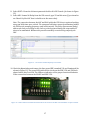
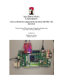
Virtex-‐6 ML605 Development Board with 4-‐DSP FMC-‐150 ADC/DAC Department of Electrical and Computer Engineering Real-‐Time DSP and FPGA lab Colin Fera Matthew Luscher Ashkan Ashrafi Figure 1 – ML605 and FMC-‐150 Introduction ............................................................................................................................................ 2 Project Specific Customizations ....................................................................................................... 3 Requirements ......................................................................................................................................... 4 Software Requirements ................................................................................................................................ 5 Hardware Requirements .............................................................................................................................. 5 Limitations and Specifications ................................................................................................................... 5 Setup .......................................................................................................................................................... 6 Hardware ........................................................................................................................................................... 7 Connecting the ML605 and FMC-‐150 .................................................................................................... 7 Connecting the Waveform Function Generator .............................................................................. 10 Block Diagram ................................................................................................................................................ 11 Software .......................................................................................................................................................... 12 Running the Design ........................................................................................................................... 14 Verification of Setup .................................................................................................................................... 15 Implementation a Digital FIR Filter using Xilinx ISE ........................................................................ 19 Process .............................................................................................................................................................. 19 Instantiation ................................................................................................................................................... 25 Verification ...................................................................................................................................................... 26 Appendix ............................................................................................................................................... 28 Running the ML605 Reference Design In ISE13.1 ............................................................................. 29 Designing a Digital LPF in MATLAB ........................................................................................................ 30 Process .............................................................................................................................................................. 30 MATLAB Code ................................................................................................................................................ 33 MATLAB Filter Coefficients ...................................................................................................................... 34 References ............................................................................................................................................ 36 Introduction The purpose of this tutorial is to help familiarize readers with the use of the AVNET Xilinx Virtex 6 based ML605 development kit and in particular the accompanying 4-‐DSP FMC-‐150 analog to digital converter (ADC) and digital to analog converter (DAC) for real time digital signal processing (DSP) applications. This tutorial assumes familiarity with hardware description languages (HDL’s) and basic concepts of digital signal processing. By following this tutorial and using the accompanying VHDL\Verilog code the reader should be able to: • Configure the DAC to pass data through from the ADC • Implement a basic Low pass filter with the aid of MATLAB (Located in the appendix) Portions of this tutorial have been taken from various AVNET and Xilinx tutorials and documentation accompanying the board. Document names as well as links are provided in the references section at the end of this document. 2 Project Specific Customizations •
•
•
•
•
Project based on AVNET RTL Reference Design Tutorial (Available through their website for ISE 13.1). Sampling rate changed to the maximum supported by the internal clock of the FMC-‐
150 at 245.11MHz. The Digital Up Converter (DUC), Digital Down Converter (DDC), and Direct Digital Synthesizer (DDS) IP Cores, and supporting code, were removed as they were not needed for the purposes of this tutorial; however, if you wish to follow the aforementioned tutorial of which this project is based on, the DUC, DDC, and DDS are an integral part of their (AVNET) tutorial and must be implemented in the project provided with this tutorial. An order 80 digital low-‐pass filter is implemented in addition to this tutorial as a reference to verify the functional behavior this tutorial. See Appendix The project file, originating in ISE 13.1, was moved to ISE 14.4p by the means of instantiating the minimum required IP cores for the demonstration purposes of this tutorial, which suggests not all the IP cores in this project are a necessity for proper functional behavior (i.e. the aforementioned LPF). 3 Requirements This section reviews the minimum hardware and software requirements needed to successfully complete the tutorial. 4 Software Requirements •
•
ISE 14.4p (Latest version available when this documents was created. See Code Customizations section for pseudo-‐instructions on moving the ISE project, and dependencies, to a different version of ISE.) MATLAB (Optional for design of LPF as mentioned in the Appendix. Also, MATLAB requires the DSP toolbox.) (Note: Xilinx ISE must be a fully licensed product. The free web pack will not work.) Hardware Requirements •
•
•
•
•
•
•
AVNET Xilinx ML605 Development Kit 4-‐DSP FMC-‐150 ADC/DAC Waveform Signal Generator Oscilloscope (2-‐ 3 channel) MMCX to BNC Coax Cable (Qty 3) BNC to BNC Coax Cable BNC Splitter Limitations and Specifications A key limitation of the FMX-‐150 is the ADC/DAC is AC coupled effectively creating a high-‐
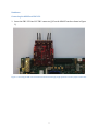
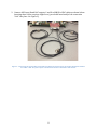
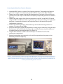
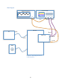
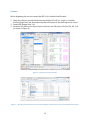
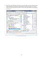
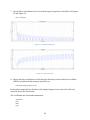
pass filter and imposes bandwidth limitations on the hardware. In addition, the DAC has an 82MHz 5th order Chebyshev low-‐pass filter on its output. Listed below summarizes the useful reliable-‐operational bandwidths, as well as some key limitations, outlined in the FMC-‐150 user manual. ADC • Bandwidth: 400KHz -‐ 250MHz • Input voltage range: 2Vp-‐p (note: the gain is adjustable so achieve a 1Vp-‐p range) DAC • Bandwidth 3MHz -‐ 82MHz • Output voltage range: 1Vp-‐p 4-‐DSP, the manufacturer of the FMC-‐150, offers a service to convert the FMC-‐150 ADC/DAC to DC coupling. In addition, they can alter the low pass filter on the DAC. The unit would have to be sent in for the modifications at a cost. 5 Setup The following instructions will guide the reader through the setup of the aforementioned required hardware and software for this tutorial. 6 Hardware Connecting the ML605 and FMC-‐150 1. Insert the FMC-‐150 into LPC FMC connector (J63 on the ML605 board as shown in Figure 1). Figure 2 – Inserting the FMC-‐150 board into the ML605 board. Apply slight pressure to ensure proper connection. 7 2. Connect ADC input B and DAC outputs C and D to MMCX to BNC cables as shown below. Inserting these cables requires slight force (you should heard and feel the connection “click” into place. See Figure 2). Figure 3 – Connecting the signal cables to the FMC-‐150. When inserted properly, the reader should feel and hear the cables “click” into place. Inputs A and External Clock are not used in this tutorial. 8 3. Connect a mini-‐B USB cable to the USB female J22 on the ML605 labeled JTAG (As shown in Figure 4). Connect the other end to your computer. 4. Set the dipswitches on the lower right corner ML605 board, adjacent to the USB, to all OFF. Figure 4 – Connect a mini-‐B USB cable to the ML605 board and connect the other end to the PC with ISE currently running. 9 Connecting the Waveform Function Generator 1. Attach the BNC splitter to output of the function generator. This enables the function generator’s output to be observed in parallel with the output of the FMC-‐150 DAC. 2. Connect one of the outputs from the function generator to an input of the oscilloscope (Channel one of the scope is connected to the output of the function generator as shown in Figure 6). 3. Connect the other output of the function generator to the ADC on the FMC-‐150 board using the MMCX to BNC Coax Cable on port A (Or port B, but note which port the function generator is connected to because it will referenced later in this tutorial for specific configuration of the port). 4. Turn on the function generator and oscilloscope and set the function generator to output a 1Vp-‐p sine wave at 5MHz. 5. Set the oscilloscope to display the waveform to verify proper connection. Using the Auto Set feature on the oscilloscope should provide you with a decent-‐viewable window of the signal from the function generator (See Figure 4). 6. Connect DAC channels C and D to the oscilloscope on channels 2 and 3 of the oscilloscope; respectively. 7. Ensure the waveform is as expected on the oscilloscope and turn the power to the board on (As shown in Figure 5). Figure 5 – 1) Connection to the oscilloscope with attached BNC splitter on the output of the function generator. 2) Connection of the function generator to the input of the ADC on port A of the FMC-‐150 board (connection of the MMCX to the FMC-‐150 board not shown here, please see Figure 2). Refer to the documentation provided with the oscilloscope and function generator as needed. 10 Block Diagram Oscilloscope Signal Generator Ch 1 Ch 3 ML605 USB PC Ch 2 Port D FMC-‐150 JTAG Port C Port A PWR Diagram 1 – Block diagram of how to setup should look. 11 Software Before beginning this section ensure that ISE 14.4 is installed and licensed. 1. Unzip the software provided with this tutorial (fmc150_ISE_14_4.zip) to a suitable location (Experience has shown that locations with spaces in the path may cause issues). 2. Launch ISE Design Suite 14.4 3. From the File Menu, select Open Project and locate the ISE project file ‘fmc150_ISE_14_4’ (as shown in Figure X) Figure 6 – Opening the project from ISE. Figure 7 – Open the project from the location of the unzipped contents of the project provided with this tutorial. 12 4. Select the top file ML605_fmc150 and in the process window (directly below the Design Hierarchy), double click Generate Programming File (As shown in Figure 8). This will synthesize the design producing a bit file. This step takes approximately three minutes to complete. Figure 8 – Select the top module from the Design pane and double click Generate Programming File to generate a bit file and synthesize the design. 13 Running the Design In this part of the tutorial you will program the FPGA with the bit file created in the Preparing the Software section. You will then configure ADC channel(s) for optimal performance. Finally you will pass a sine wave into the ADC from the function generator where it will be output by the DAC and viewed on the oscilloscope. 14 Verification of Setup 1. With the Xilinx project navigator open from the last step of Preparing the Software, double click on Analyze Design Using ChipScope (A window should popup as shown in Figure 9). 2. In the upper left of the ChipScope Pro window, click the icon. This icon opens the JTAG search chain and searches for Xilinx cores. 3. Two devices should be detected (displayed in the-‐most pane of the ChipScope window), DEV: 0 and DEV: 1. 4. Right click DEV: 1 and select Configure (As shown in Figure 9). Figure 9 – This window will appear only after a bit file has been generated and the reader clicked on Analysis Design using Chipscope. This figure shows what you should expect to see in the left pane after step two from above. 15 5. After clicking on Configure, Click Select New File and locate ‘ml605_fmc150.bit’ 6. Select open then select OK. This is the bit file that was generated in Preparing the Software. This will program the FPGA using the selected bit file. (Note, if the board is power cycled, the board must be reprogrammed). See Figure 10. 7. The FPGA is now programmed and you should expect to see the ChipScope Pro left-‐
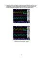
most pane populate (As shown in Figure 11). Figure 10 – Select the generated bit file generated in Preparing the Software. Figure 11 – After the FGPA is programmed, the lost-‐most pane should populate with relevant information regarding the detected-‐programmed devices. 16 8. Select UNIT: 0 from the left-‐most pane and double click VIO Console (As shown in Figure 12). 9. Select ADC channel A iDelay from the VIO console, type 25 and hit enter (If you intend to use Chanel B of the ADC then it should set to the same value). Note: The connection between the ADC and DAC within the FPGA is not registered making setup and hold times more critical. The setup and hold times cannot be maintained within the FPGA at the sampling frequency used in this tutorial. The iDelay (Incremental Delay) adds a sub-‐clock period delay to the clock at critical points allowing the setup and hold times to be maintained. Without this you will essentially see noise being output by the DAC. Figure 12 – VIO Console within ChipScope Pro window. 10. Check the dipswitches and ensure the four green LED’s numbed 5-‐8 are illuminated (As shown in Figure 13). The green LEDs indicate the clocks on the FMC-‐150 and FPGA are phase-‐locked; this is critical. The LEDs are indicative of the proper functional behavior of the connection between the ML605 and FMC-‐150 . Figure 13 – LEDs 5-‐8 must be illuminated and indicate the clocks on the FMC-‐150 and ML605 are phase-‐locked. 17 11. Activate channels one and two on the oscilloscope, if not done so already, and verify that a sine wave at the previously set frequency of 5MHz is displayed on both channels. (As shown in Figure 14) Figure 14 – The yellow signal shown in this figure is the output of the function generator and the blue signal is the signal from the DAC of the FMC-‐150 board. Note: Using the BNC splitter with transmission lines at differing lengths is far from ideal. The sine waves displayed will not be identical but will be similar (As shown in Figure 14). The output from the DAC will be out of phase with respect to the function generator’s output and have different amplitudes, which should be within about 30% of the function generator’s measured reference signal, but the frequency and form should be very similar. This completes this portion of the tutorial. 18 Implementation a Digital FIR Filter using Xilinx ISE Process 1. First create the COE file; this file initializes the block memory with the filter coefficients. To change the filter coefficients this file will need to be reimported each time. The format of the file is as follows: The semicolon character ends every command and can also be used to denote comments. Any characters following the semicolon up until the next line return is ignored. The file should be saved in ASCI format with file extension .coe. radix=16; ; Denotes that the filter data is hex, other options are 2 or 10 ; for binary or decimal respectively. The following is the coefficient vector, one coefficient should appear on each line the lines are terminated with a comma until the last line that is terminated with a semicolon. The file can have any number of coefficients between 1 and over 200 depending on which IP core version and options are selected. The number of coefficients dictates the order of the filter. COEFDATA= fff1, ffe5, fff1; 2. Right click on the IP Core called lowpass and select remove and then ok. In the next part of this tutorial we will recreate this IP core. 19 Figure 15 – Removing the original LPF. 3. Right click anywhere in the design hierarchy window and select New Source 4. Click IP (CORE Generator and Architecture Wizard), type the name lowpass under the filename field and select next. 20 Figure 16 -‐ New source -‐> IP 21 5. When prompted, select yes to overwrite the existing core named lowpass. 6. Expand the view to Digital Signal Processing, then Filters and highlight FIR Compiler (version 5.0, as shown in Figure 19) and click next and then finish. Figure 17 – Selecting a IP core 22 7. Click the vector drop down and change this to COE file, then click the browse button and select the COE file created in step 1. The COE file will be imported and the coefficients file field will show a path. If this area is highlighted in red then there may be an issue with the format of this file. 8. Fill in the input sampling frequency and clock frequency in this case they are 245.76 and 491.52 respectively. The first page of the fir compiler menu should look as shown below. Figure 18 – Defining the filter. 23 9. Click next to move on to page 2 of the FIR compiler menu. 10. Change the input data width to 14 (Note the FMC-‐150 has a 14Bit ADC) 11. Change output rounding mode to any choice other than full precision, in this case we have chosen symmetric rounding to zero. 12. Change the output width to 16 all other choices can be left at the default values as shown below. Figure 19 – FIR Compiler Widow 13. At this point, since no other options need to be changed from the default values click generate. This will generate the IP core; the process takes about 1-‐2 minutes. 14. The filter IP core you created should be visible under the Verilog module sample_pass_inst; this indicates that the filter is being instantiated under that module as shown below. This concludes this part of the tutorial. 24 Instantiation This code below is the actual sample_pass_inst where the filter in this tutorial is being instantiated. Note the multiplexers that control how data is routed between inputs and outputs and also between the inputs and the filter. The dipswitches that control the multiplexers are numbered one through eight, and are shown in Figure 25. module sample_pass( input clk_fs,clk_gfs, input [13:0] din_a,din_b, output [15:0] dout_a,dout_b, input [7:0] gpio_dip_sw ); //wires used in IO Muxes wire [13:0] dinf; wire [15:0] doutf; //IO Muxes select how inputs are passed to outputs. assign dout_a = (gpio_dip_sw[1:0] == 1) ? doutf : (gpio_dip_sw[1:0] == 2) ? {din_b,2'b00} : {din_a,2'b00}; assign dout_b = (gpio_dip_sw[3:2] == 1) ? doutf : (gpio_dip_sw[3:2] == 2) ? {din_a,2'b00} : {din_b,2'b00}; //combinational assignment of the either input A or B to the filter assign dinf = (gpio_dip_sw[5]) ? din_a : din_b; //the actual instantiation of the filter. lowpass fir1 (.din(dinf),.dout(doutf),.clk(clk_gfs)); endmodule Figure 20 – Dipswitches. 25 Verification At this point it is assumed that all previous tutorial sections have been completed • Setup o Preparing the Hardware o Preparing the Waveform Signal Generator o Preparing the Software • Design a Simple Digital Filter using MATLAB • Implement a Digital FIR Filter using ISE 1. Ensure your setup identical to Diagram 1 in the Preparing the Hardware section. 2. Activate channels one, two and three on the oscilloscope and verify that a sine wave at the previously set frequency is displayed on all three channels (As shown in figure 22. Note, the purple signal is the signal being passed through the filter. Its appearance should look very similar because the frequency of the signal from the function generator has not been tuned to the cutoff frequency of the filter). Figure 21 – Expected signals displayed on the oscilloscope. 3. Record the peak amplitude of the filtered sine wave to verify the cutoff frequency when you increase the frequency of the signal later in the instructions.. 4. Increase the frequency of the function generator until the amplitude of the filtered signal drops to .707*Vpeak (of the reference signal). This is the -‐3DB point at which signal power has fallen by half its original voltage denoting the start of the filter’s cutoff frequency. 5. Compare this point to the -‐3DB frequency shown in the MATLAB plot; they should similar, but not exact. 26 6. Continue to increase the frequency of the function generator beyond the filter cutoff. The amplitude of the filtered signal should fall gradually to zero as the frequency is increased towards the stop frequency (As shown in Figure 23 and Figure 24). Figure 22 -‐ Function generator output at 7Mhz. Figure 23 – Function generator output at 9Mhz. This concludes this part of the tutorial. 27 Appendix The appendix of the tutorial provides the reader with additional tutorials and documentation. 28 Running the ML605 Reference Design In ISE13.1 The purpose of this section is to provide notes regarding the process of running of the ML605 reference design tutorials provided by AVNET. You can obtain the ML605 reference design tutorial of your choice from: http://www.xilinx.com/products/boards-‐and-‐kits/EK-‐V6-‐ML605-‐G.htm Notes: •
•
•
•
•
•
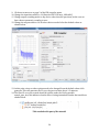
•
The reference designs do not work in any version of ISE newer than 13.1. Only the tutorial instructions themselves are different. The project code included with this tutorial is a minimization of the actual code from AVNET. Even if using ISE 13.1, some IP cores cannot be opened because they are not fully supported. You can obtain code versions of the tutorial for ISE back to 12.2 (from the link above). The IP cores in these versions can be opened/modified. The tutorial is unusable until the ADC CH A and B iDelay’s are set, as demonstrated in the main tutorial. These should be set as soon as the ML605 board has been programed using ChipScope. The recommended value is approximately 25. While running the tutorial o The DAC outputs a constant ~12MHz sinusoid. This acts as a function generator to drive the ADC which is then viewed in ChipScope. o Dipswitch 3 can be switched to bypass the digital up converter and digital down converter such that the ADC input is passed directly out of the DAC output. The sampling frequency used by the tutorial is 66.44MHz 29 Designing a Digital LPF in MATLAB Process In this part of the tutorial you will generate a simple digital low pass filter using MATLAB. The filter will have quantized 16bit coefficients, such that it can be readily implemented on the FPGA. The MATLAB script used to generate this filter is appendix A of this document. The following enumerated steps are provided the reader with a better understanding of the creation 1. First you must decide upon the specifications of your filter. For this particular filter we will specify: order, sampling frequency, pass band and stop band frequencies. • A high filter order is recommended, here will use order 80. This ensures that the filter cutoff is relatively sharp. • Pass band is the frequency at which the signal begins to roll off; here we chose 5MHz. • Stop band is the frequency at which the signal will be totally attenuated; here we chose 9MHz. • Sampling frequency is the frequency of sampling on the ADC. The code provided with this tutorial sets the sampling frequency at 245.11MHz 2. Save the filter specifications as variables in MATLAB. fp = 5e6; %freq at beging of pass band = 5MHz fst = 9e6; %freq at end of stop band = 9MHz n=80; %filter order = 80 fs=245e6; %sampling frequency = 245MHz 3. Save the filter specifications in a MATLAB data structure f=fdesign.lowpass('N,Fp,Fst',80,fp,fst,fs) f = Response: 'Lowpass' Specification: 'N,Fp,Fst' Description: {'Filter Order';'Passband Frequency';'Stopband Frequency'} NormalizedFrequency: false Fs: 245000000 FilterOrder: 80 Fpass: 5000000 Fstop: 9000000 4. Generate the low pass filter. h = design(f, 'firls', 'Wpass', 1, 'WStop', 100, 'FilterStructure', 'dffir'); 30 5. Change the data format for the filter that was just created to fixed. %set filter to fixed type set(h,'Arithmetic','fixed'); 6. Review the specifications of the filter that was just created. h = FilterStructure: 'Direct-‐Form FIR' Arithmetic: 'fixed' Numerator: [1x81 double] PersistentMemory: false CoeffWordLength: 16 CoeffAutoScale: true Signed: true InputWordLength: 16 InputFracLength: 15 FilterInternals: 'FullPrecision' 31 7. Use the filter visualization tool to view the frequency response of the filter. See Figures 15 and Figure 16. hfvt = fvtool(h); Figure 24 – Magnitude Response Figure 25 – Phase Response 8. Export the filter coefficients as 16bit hex such that they can be readily use in a Xilinx COE file to initialize block memory in an FIR core. fcfwrite(h,'simple_lowpass','hex') In the above command, h is the filter itself, simple_lowpass is the name of the file to be exported, hex is the data format. The coefficients are listed under numerator: Numerator: fe6b fd99 fca3 ....... 32 MATLAB Code %The following script: %-‐Sets parameters for a simple digital low pass filter %-‐Generates the low pass filter %-‐Displays the filters response graphically %-‐Retrieves hex coefficients which can be directly used in a COE file % fp = 5e6; %freq at beging of pass band = 5MHz fst = 9e6; %freq at end of stop band = 9MHz n=80; %filter order = 80 fs=245e6; %sampling frequency = 245MHz %Instruct MATLAB to design the filter specified above f=fdesign.lowpass('N,Fp,Fst',80,fp,fst,fs); % Generate a direct form low pass filter using above specifications h = design(f, 'firls', 'Wpass', 1, 'WStop', 100, ... 'FilterStructure', 'dffir'); %set filter to fixed type set(h,'Arithmetic','fixed'); %use the filter visualization tool to hfvt = fvtool(h); %retrieve filter coefficients as hex list fcfwrite(h,'simple_lowpass','hex') 33 MATLAB Filter Coefficients % Generated by MATLAB(R) 7.12 and the Signal Processing Toolbox 6.15. % Generated on: 19-‐May-‐2013 16:44:36 % Coefficient Format: Hexadecimal % Discrete-‐Time FIR Filter (real) % -‐-‐-‐-‐-‐-‐-‐-‐-‐-‐-‐-‐-‐-‐-‐-‐-‐-‐-‐-‐-‐-‐-‐-‐-‐-‐-‐-‐-‐-‐-‐ % Filter Structure : Direct-‐Form FIR % Filter Length : 81 % Stable : Yes % Linear Phase : Yes (Type 1) % Arithmetic : fixed % Numerator : s16,19 -‐> [-‐6.250000e-‐02 6.250000e-‐02) % Input : s16,15 -‐> [-‐1 1) % Filter Internals : Full Precision % Output : s36,34 -‐> [-‐2 2) (auto determined) % Product : s31,34 -‐> [-‐6.250000e-‐02 6.250000e-‐02) (auto determined) % Accumulator : s36,34 -‐> [-‐2 2) (auto determined) % Round Mode : No rounding % Overflow Mode : No overflow Numerator: fe6b fd99 fca3 fb8b fa57 f90c f7b4 f659 f507 f3ce f2bc f1e2 f151 f11b f14e f1fc f333 f4fe f766 fa72 fe24 027c 0774 0d02 1319 19a7 2096 27cf 2f34 36a8 3e0a 34 453a 4c16 527e 5853 5d78 61d4 654f 67d9 6965 69e9 6965 67d9 654f 61d4 5d78 5853 527e 4c16 453a 3e0a 36a8 2f34 27cf 2096 19a7 1319 0d02 0774 027c fe24 fa72 f766 f4fe f333 f1fc f14e f11b f151 f1e2 f2bc f3ce f507 f659 f7b4 f90c fa57 fb8b fca3 fd99 fe6b 35 References [1] No author provided. 2010. Xilinx Vertex-‐6 DSP Development Kit with High-‐Speed Analog. Available: https://www.em.AVNET.com/Support%20And%20Downloads/virtex6dsp_rtl_referen
ce_design_tutorial_13_1.zip [2] No author provided. 2010. FMC150 User Manual. Available: https://www.em.AVNET.com/Support%20And%20Downloads/FMC150_user_manual.
pdf 36