1
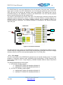
FMC150 User Manual r1.9 FMC150 User Manual 4DSP LLC, USA Email: [email protected] This document is the property of 4DSP LLC and may not be copied nor communicated to a third party without the written permission of 4DSP Inc. © 4DSP LLC 2010 FMC150 User Manual r1. Revision History Date Revision Revision 2010-08-13 Initial Draft 0.1 2010-08-13 Release after review 1.0 2010-10-20 Update oscillator details in the clock description. Removed DIP switch definition 2010-10-21 Changed order code scheme 1.2 2010-11-15 Correction in block diagram 1.3 2011-01-14 Correction of section 4.2.3 1.4 2011-01-21 Updated input/output bandwidth specification 1.5 2012-01-10 Removed TBD from document. Updated performance numbers 1.6 2012-10-08 Added changes between revision 1 and revision 2 boards 1.7 2013-07-16 Reworded the description of the DAC output filter option 1.8 2014-03-17 Reworded some descriptions and fixed typos 1.9 tree 1.1 FMC150 User Manual July 2013 www.4dsp.com -2- FMC150 User Manual r1. Table of Contents 1 2 3 4 5 6 7 8 9 Acronyms and related documents ................................................................................ 5 1.1 Acronyms ................................................................................................................... 5 1.2 Related Documents .................................................................................................... 5 General description ........................................................................................................ 6 Installation ...................................................................................................................... 7 3.1 Requirements and handling instructions ..................................................................... 7 Design ............................................................................................................................. 7 4.1 Physical specifications ............................................................................................... 7 4.1.1 Board Dimensions ............................................................................................... 7 4.1.2 Front panel .......................................................................................................... 8 4.2 Electrical specifications .............................................................................................. 8 4.2.1 EEPROM ............................................................................................................ 9 4.2.2 JTAG................................................................................................................... 9 4.2.3 FMC Connector ................................................................................................... 9 4.3 Main characteristics.................................................................................................... 9 4.4 Analog input channels .............................................................................................. 11 4.5 Analog output channels ............................................................................................ 11 4.6 External trigger input ................................................................................................ 11 4.7 Clock tree ................................................................................................................. 11 4.7.1 External clock input ........................................................................................... 11 4.7.2 Architecture ....................................................................................................... 11 4.7.3 PLL design ........................................................................................................ 12 4.8 Power supply............................................................................................................ 13 Controlling the FMC150................................................................................................ 14 5.1 Guidelines for controlling the clock tree .................................................................... 14 5.2 Guidelines for controlling the ADC............................................................................ 14 5.3 Guidelines for controlling the DAC............................................................................ 14 5.4 Guidelines for controlling onboard monitoring........................................................... 14 5.5 Controlling on-board FANs ....................................................................................... 15 Environment.................................................................................................................. 15 6.1 Temperature ............................................................................................................ 16 6.2 Monitoring ................................................................................................................ 16 6.3 Cooling ..................................................................................................................... 16 6.3.1 Convection cooling ............................................................................................ 16 6.3.2 Conduction cooling ............................................................................................ 16 Safety............................................................................................................................. 16 EMC ............................................................................................................................... 16 Ordering information .................................................................................................... 18 FMC150 User Manual July 2013 www.4dsp.com -3- FMC150 User Manual r1. 10 Warranty ........................................................................................................................ 18 Appendix A. LPC pin-out ..................................................................................................... 19 FMC150 User Manual July 2013 www.4dsp.com -4- FMC150 User Manual r1. 1 Acronyms and related documents 1.1 Acronyms ADC DDR DSP EPROM FBGA FMC FPGA JTAG LED LVTTL LSB LVDS MGT MSB PCB PCI PCIe PLL PMC PSSR QDR SDRAM SRAM TTL XMC Analog-to-Digital Converter Double Data Rate Digital Signal Processing Erasable Programmable Read-Only Memory Fineline Ball Grid Array FPGA Mezzanine Card Field Programmable Gate Array Join Test Action Group Light Emitting Diode Low Voltage Transistor Logic level Least Significant Bit(s) Low Voltage Differential Signaling Multi-Gigabit Transceiver Most Significant Bit(s) Printed Circuit Board Peripheral Component Interconnect PCI Express Phase-Locked Loop PCI Mezzanine Card Power Supply Rejection Ratio Quadruple Data rate Synchronous Dynamic Random Access memory Synchronous Random Access memory Transistor Logic level PCIe Mezzanine card Table 1: Glossary 1.2 Related Documents FPGA Mezzanine Card (FMC) standard ANSI/VITA 57.1 Datasheet ADS62P49 Rev 2009/06, Texas Instruments Datasheet DAC3283 Rev 2010/04, Texas Instruments Datasheet CDCE72010 Rev 2010/06, Texas Instruments Datasheet ADS4249 Rev 0.2 2010/03, Texas Instruments Datasheet AMC7823, Texas Instruments FMC150 User Manual July 2013 www.4dsp.com -5- FMC150 User Manual r1. 2 General description The FMC150 is a four-channel, ADC/DAC FMC daughter card. The card provides two 14-bit A/D channels and two 16-bit D/A channels, which can be clocked by an internal clock source (optionally locked to an external reference) or an external sample clock. In addition, there is one trigger input for customized sampling control. The FMC150 daughter card is mechanically and electrically compliant to FMC standard (ANSI/VITA 57.1). The FMC150 has a low-pin count connector and front panel I/O. It can also be used in a conduction-cooled environment. The design is based on TI’s ADS62P49/ADS4249 dual-channel 14-bit 250Msps ADC and TI’s DAC3283 dual channel 16-bit 800Msps DAC. The AC-coupled analog signal inputs are connected to MMCX/SSMC coax connectors on the front panel. The FMC150 allows flexible control of sampling frequency, analog input gain, and offset correction through serial communication busses. Furthermore, the card is equipped with power supply and temperature monitoring, and it offers several power-down modes to switch off unused functions. Channel A AC Coupling A/D AC Coupling ADS62P49/ ADS4249 LVDS Data (14) Control 250 Msps, 14-bit Monitoring AMC7823 External Clock / Reference Clock tree LVDS Clock (1) Control External Trigger CDCE72010 LVDS Trigger (1) Channel C AC Coupling D/A Channel D AC Coupling LVDS Clock (1) DAC3283 LVDS Data (8) 800 Msps, 16-bit LVDS Frame (1) FMC Low-Pin Count 160-pins LVDS / LVCMOS 2.5V Channel B LVDS Clock (1) Control Figure 1: FMC150 block diagram FMC150 User Manual July 2013 www.4dsp.com -6- FMC150 User Manual r1. 3 Installation 3.1 Requirements and handling instructions Prevent electrostatic discharges by observing ESD precautions when handling the card. Do not flex the card, and do not exceed the maximum torque specification on the coax connectors. The FMC150 daughter card must be installed on a carrier card compliant to the FMC standard. The FMC carrier card must support the low-pin count connector (160-pins). The FMC carrier card may support the high-pin count connector (400-pins). The carrier card must support VADJ/VIO_B voltage of +2.5V (LVDS support) for FMC150 revision 1. The carrier card can support VADJ/VIO_B voltage range of 1.65V to 3.3V for FMC150 revision 2, but VADJ voltage range will typically be 1.8V or 2.5V for LVDS operation. 4 Design 4.1 Physical specifications 4.1.1 Board Dimensions The FMC150 card complies with the FMC standard known as ANSI/VITA 57.1. The card is a single-width, conduction-cooled mezzanine module (with region 1 and front panel I/O). The front area holds six MMCX or six SSMC connectors. The stacking height is 10mm. FMC150 User Manual July 2013 www.4dsp.com -7- FMC150 User Manual r1. D DAC C TRG CDCE CLK B ADC A AMC Figure 2 : FMC150 dimensions 4.1.2 Front panel There are six MMCX or SSMC connectors available from the front panel. From top to bottom: analog in A, analog in B, clock in (CLK), trigger in (TRG), analog out C, and analog out D. Figure 3: Bezel design 4.2 Electrical specifications The FMC150 uses high-speed LVDS outputs. Revision 1 boards require +2.5V on VADJ power supply (supplied by the carrier card). Revision 2 boards can operate with a VADJ voltage range of 1.65V to 3.3V, but typically VADJ will be 1.8V or 2.5V for LVDS operation. FMC150 User Manual July 2013 www.4dsp.com -8- FMC150 User Manual r1. The voltage on VIO_B pins will be at the same level as VADJ as it is connected directly to VADJ on the FMC150. The data converters operate in LVDS mode (clock and data pairs). All other status and control signals, like serial communication busses, operate at LVCMOS level (VOH = VADJ). 4.2.1 EEPROM The FMC150 card carries a 2Kbit EEPROM, which is accessible from the carrier card through the I2C bus. The EEPROM is powered by 3P3VAUX. The standby current is only 0.01µA when SCL and SDA are kept at 3P3VAUX level. The EEPROM is write-protected. 4.2.2 JTAG The FMC150 card TDO pin is connected to the TDI pin to ensure continuity of the JTAG chain. TCK, TMS, and TRST are left unconnected on the FMC150. 4.2.3 FMC Connector The low-pin count connector has only bank LA available and two dedicated LVDS clock pairs. The recommendations from AV57.1 Table 14 have been taken into account, resulting in the following arrangement: The clock and data pairs from the ADC are mapped to LA00_CC and LA01-LA14, respectively. The remaining connections from the associated I/O signals (LA15-LA16) are used for non-critical control signals. The reference clock for the DAC interface is mapped to CLK0_M2C. The clock, frame, and data pairs to the DAC are mapped to LA17-LA26. The remaining connections from the associated I/O signals (LA27-LA33) are used for non-critical control signals. The external trigger connects to CLK1_M2C. Refer also to Appendix A. LPC pin-out. 4.3 Main characteristics Analog Inputs Number of channels 2 Channel resolution 14-bit Input voltage range 2Vp-p (10 dBm) Input gain Input impedance Analogue input bandwidth SNR Programmable from 0dB to 6dB in 0.5dB steps (6dB gain gives an input voltage range of 1Vp-p) 50Ω (AC-coupled) 0.40-500MHz 71dBFS @ 45MHz Fin FMC150 User Manual July 2013 www.4dsp.com -9- FMC150 User Manual SFDR r1. 80dBc @ 45MHz Fin Analog Outputs Number of channels 2 Channel resolution 16-bit Output voltage range 1Vp-p Output impedance Analog output bandwidth THD 50Ω (AC-coupled) 82MHz 5th order Chebyshev low-pass filter Slope / Roll-Off = -124.9 dB / decade Difference between the signal strengths at 65 MHz and 75 MHz = 0.6 dB Output filter can be bypassed by 4DSP. Please contact sales for this option. Low cutoff is 3MHz due to the output transformer stage. -67 dBc External Clock/Reference Input Input Level 0.1 – 1.3 Vp-p Input impedance 50Ω (AC-coupled) Input bandwidth 3-800MHz (Reference clock limited to 500MHz) External Trigger input Format Frequency range LVTLL/LVCMOS Logic ‘0’ max 0.8V / Logic ‘1’ min 2.0V Up to 125 MHz ADC Output Data width LVDS 7-pairs DDR per channel Data Format Offset binary or 2’s complement Sampling Frequency Range up to 250MHz DAC Input Data width Data Format Sampling Frequency Range LVDS 8-pairs DDR Offset binary or 2’s complement up to 800MHz Internal Sampling Clock Format Frequency Range LVPECL 491.52 MHz (contact factory for different frequency options) ADC: 245.76 MHz (contact factory for different frequency options) DAC: 491.52 MHz (contact factory for different frequency options) Table 2 : FMC150 daughter card main characteristics FMC150 User Manual July 2013 www.4dsp.com - 10 - FMC150 User Manual 4.4 r1. Analog input channels The AC-coupled input uses wideband RF transformers (TC1-1T). Two transformers are used to compensate for imbalance and reduce harmonic distortion. A capacitor in front of the transformer blocks the DC path to ground. This protects the signal source if a DC-coupled signal with offset is accidentally connected to the FMC150. The input impedance is matched to 50Ω behind the transformers by terminating each node to the common mode voltage of the ADC. The R-C-R filter near the input of the A/D converter can be used to improve performance when lower input bandwidth is required. This filter is assembled by default. 4.5 Analog output channels The AC-coupled output uses wideband RF transformers (TC4-1W). An optional reconstruction filter is available on each DAC output. Refer to Table 2 for the filter characteristics. The filter can optionally be bypassed on the board by 4DSP. Please contact sales for details on this option. Figure 4: Optional DAC reconstruction filter 4.6 External trigger input The external trigger input is configured as a single-ended input. The allowed input range is ground and 3.3V. The trigger threshold is set to 1.65V 4.7 Clock tree 4.7.1 External clock input There is one clock input on the front panel that can serve as a sampling clock input or as a reference clock input if the internal clock is desired. Note: When the internal clock is enabled and there is no need for an external reference, it is highly recommended to disconnect the external clock input to prevent interference with the internal clock. 4.7.2 Architecture The clock architecture of the FMC150 card combines flexibility and high performance. Components have been chosen to minimize jitter and phase noise and reduce degradation of the data conversion performance. The user may choose to use either an external or internal sampling clock. FMC150 User Manual July 2013 www.4dsp.com - 11 - FMC150 User Manual r1. TI’s CDCE72010 PLL and clock distribution device is the base of the clock tree. The external clock input is routed to two RF transformers: one for driving the reference input of the PLL (SEC_IN) and one for driving the auxiliary clock input (AUXIN). The auxiliary input can be connected directly to the distribution section of the CDCE72010. The VCO can be powered down to avoid interference with the external clock. The VCXO is connected to the VCXO clock input. This clock input connects to both the clock distribution section and the PLL section. In order to tune the VCXO to a certain frequency, a reference clock is required. An onboard 100MHz oscillator can be enabled if there is no external reference connected. The onboard oscillator is connected to the primary reference input (PRI_IN). CDCE72010 XTAL 100MHz LVPECL ADC Clock IN [assembly option] To FMC VCXO DAC AUXIN Figure 5: Clock tree architecture The A/D and D/A clock outputs on the CDCE72010 should be configured as LVPECL outputs. Another output is configured as the LVDS output and connects to the FMC connector to supply reference clock for the D/A clock and data signals (CLK_TO_FPGA_P/N). 4.7.3 PLL design The PLL functionality of the CDCE72010 operates from an internal sampling clock. To enable flexibility in frequency selection while maintaining high performance, a high frequency low phase noise VCXO is used. A high frequency oscillator enables different output frequencies after division. The design allows different VCXO types: 1) VS-705-491.52 MHz (default) a. enabling 245.76 MHz A/D sampling (divide by 2) b. enabling 491.52 MHz D/A sampling (divide by 1) 2) VS-705-737.28 MHz (contact 4DSP) a. enabling 245.76 MHz A/D sampling (divide by 3) b. enabling 737.28 MHz D/A sampling (divide by 1) FMC150 User Manual July 2013 www.4dsp.com - 12 - FMC150 User Manual r1. Figure 6: PLL1 loop filter design Reference Value Chip Resistor Size C52 100 nF 0603 R47 4.7 kΩ 0603 C51 22 µF 0805 R44 160 Ω 0603 C50 100 nF 0603 Table 3: Loop filter component values 4.8 Power supply Power is supplied to the FMC150 card through the FMC connector. The pin current rating is 2.7A, but the overall maximum is limited according to Table 4. Voltage +3.3V +12V VADJ (+1.8V / +2.5V) VIO_B (VADJ) # Pins Max Amps Max Watt 4 2 4 2 3A 1A 4A 1.15 A 10 W 12 W 10 W 2.3 W Table 4: FMC standard power specification The power provided by the carrier card can be very noisy. Special care is taken with the power supply generation on the FMC150 card to minimize the effect of power supply noise on clock generation and data conversion. Power plane VADJ 3P3V 12P0V 3P3VAUX (Operating) 3P3VAUX (Standby) Typical 554 mA 20 mA 368 mA 0.1 mA 0.01 µA Maximum 665 mA 100 mA 442 mA 3 mA 1 µA Table 5: Typical / Maximum current drawn from FMC carrier card FMC150 User Manual July 2013 www.4dsp.com - 13 - FMC150 User Manual r1. 5 Controlling the FMC150 Good knowledge of the internal structure and communication protocol of relevant onboard devices is required for controlling the FMC150. This document only provides guidelines for programming the devices. Refer to the datasheets listed in the Related Documents section of this manual for more detailed information. 5.1 Guidelines for controlling the clock tree Apart from enabling the onboard reference and VCXO, the whole clock tree is controlled by programming the CDCE72010 device through a serial communication bus. The following guidelines should be taken into account: 1. The internal reference is enabled by setting REF_EN to a logic 1 (high). The internal reference should only be enabled if the internal clock is used and there is no external reference applied. 2. The onboard VCXO is enabled by default, but it can be disabled through the GPIO pins on the AMC7823 (see section 5.4). This may be useful when using external clock. 3. It is recommended to disable the unused clock outputs. 4. It is recommended to disable PLL functions and VXCO input on the CDCE72010 when an external sampling clock is applied. 5. If internal clock is used, the PLL functions need to be enabled. The recommended phase detector frequency is 160kHz. If the internal reference is used, the reference divider should be set to 625. The VCO divider is set to 4608. 6. The stability of the PLL is not always guaranteed if other phase detector frequencies are used. 5.2 Guidelines for controlling the ADC Controlling the ADC enables advanced control of the digitizing process. The ADS62P49 can be programmed through a serial communication interface to change the output format or to use advanced settings such as gain control, offset correction, and several power-down modes. 1) Low-speed mode should be selected for sampling frequencies below 100Msps. 2) External reference should never be enabled. 3) Do not enable CMOS mode when there is LVDS termination on the carrier card. 5.3 Guidelines for controlling the DAC Controlling the DAC enables advanced control of the conversion process. The DAC3283 can be programmed through a serial communication interface to change the input format or to use advanced settings such as gain control, offset correction, and several power-down modes. 1) The communication bus can only be used in unidirectional mode, with SDIO as data input and ALARM_SDO as data output. 5.4 Guidelines for controlling onboard monitoring The FMC150 holds an AMC7823 for monitoring the temperature and several power supply voltages on the board. The device can be programmed and read through the SPI bus. FMC150 User Manual July 2013 www.4dsp.com - 14 - FMC150 User Manual r1. 1) The measured values must be multiplied by one or two to get the actual level. The measured value on channel 4 must be multiplied by 5.7 to get the actual level. 2) Operating the SPI bus continuously might interfere with the A/D or D/A conversion process and cause signal distortion. It is recommended to program the minimum and maximum thresholds in the monitoring devices and only read from the devices when the interrupt line is asserted (MON_N_INT). Only the first four channels can be monitored with thresholds. These are the main supplies derived from the other voltages on channel 4 to 7. N.B. The MON_N_INT interrupt is not available on FMC150 revision 2. 3) It is recommended to power down the unused features: DAC operation, precision current source, and reference buffer amplifier. 4) Internal reference must be selected. Because the AMC7823 is powered from 3.3V, only internal reference of +1.25V is allowed. 5) Only internal trigger mode is supported. Auto mode is recommended to continuously monitor channel 0 to channel 3 and verify against the programmed thresholds. Parameter: Voltage Formula Channel 0 3.3V Analog 2.0 * ADC0 Channel 1 3.3V Clock 2.0 * ADC1 Channel 2 1.8V Analog 1.0 * ADC2 Channel 3 1.8V Digital 1.0 * ADC3 Channel 4 12V 5.7 * ADC4 Channel 5 3.3V 2.0 * ADC5 Channel 6 VADJ 2.0 * ADC6 Channel 7 3.8V 2.0 * ADC7 Temperature (Ch.8) Table 6: Temperature and voltage parameters 5.5 Controlling on-board FANs The FMC150 holds two power headers which may be used to power low-profile FANs glued onto the devices. Each FAN on the FMC150 can be switched off individually by setting its control signal to a logic 1 (high). The control signals are connected to the GPIO on the AMC7823. 6 Environment FMC150 User Manual July 2013 www.4dsp.com - 15 - FMC150 User Manual 6.1 r1. Temperature Operating temperature -40°C to +85°C (Industrial) Storage temperature: -40°C to +120°C 6.2 Monitoring The AMC7823 device may be used to monitor voltage on the different power rails as well as the temperature. It is recommended that the carrier card and/or host software use the powerdown features in the devices if the temperature is too high. Normal operations can resume once the temperature is within the operating condition boundaries. 6.3 Cooling Two different types of cooling are available for the FMC150. 6.3.1 Convection cooling The air flow provided by the FMC150 chassis fans will dissipate the heat generated by the onboard components. A minimum airflow of 300 LFM is recommended. Alternatively, low profile FANs can be glued on top of the devices. Refer to section 5.5 on how to control these FANs. For standalone operations (such as on a Xilinx development kit), it is highly recommended to blow air across the FMC to ensure that the temperature of the devices is within the allowed range. 4DSP’s warranty does not cover boards on which the maximum allowed temperature has been exceeded. 6.3.2 Conduction cooling In demanding environments, the ambient temperature inside a chassis could be close to the operating temperature defined in this document. It is very likely that in these conditions the junction temperature of power-consuming devices will exceed the operating conditions recommended by the device manufacturers (mostly +85°C). While a low-profile heat sink coupled with sufficient air flow might be sufficient to maintain the temperature within operating boundaries, some active cooling will yield better results. Active cooling will also minimize downtime if the devices are disabled because of a temperature above the allowed maximum. 7 Safety This module presents no hazard to the user. 8 EMC This module is designed to operate within an enclosed host system built to provide EMC shielding. Operation within the EU EMC guidelines is not guaranteed unless it is installed within an adequate host system. This module is protected from damage by fast voltage transients originating from outside the host system which may be introduced through the system. FMC150 User Manual July 2013 www.4dsp.com - 16 - FMC150 User Manual r1. FMC150 User Manual July 2013 www.4dsp.com - 17 - FMC150 User Manual r1. 9 Ordering information Part Number: FMC150-2-1-1-1 Card Type FMC150 = 0 Temperature Range Industrial (-40oC to +85oC) = 1 Commercial (0oC to +70oC) = 2 Connector Type Standard Feature – MMCX (snap coupling) = 1 SSMC (screw coupling) = 2 Analog Signal Input Standard Feature – VCXO option 491.52MHz = 1 VCXO option 737.28MHz = 2 Custom VCXO option (contact factory) = 3 Mil-I-46058c Conformal Coating No Conformal Coating = 1 Add Conformal Coating = 2 10 Warranty Hardware Software/Firmware Basic Warranty (included) 1 Year from Date of Shipment 90 Days from Date of Shipment Extended Warranty (optional) 2 Years from Date of Shipment 1 Year from Date of Shipment FMC150 User Manual July 2013 www.4dsp.com - 18 - FMC150 User Manual r1.9 Appendix A. LPC pin-out Colors indicate _CC signal and associated I/O signal groups as recommended by AV57.1 in Table 14.