1
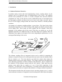
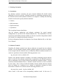
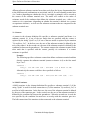
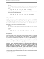
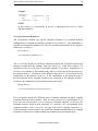
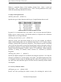
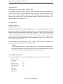
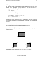
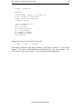
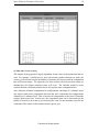
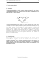
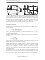
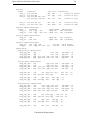
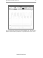
SPACE SUBSTRATE RESISTANCE EXTRACTION USER’S MANUAL A.J. van Genderen, N.P. van der Meijs, T. Smedes Department of Electrical Engineering Delft University of Technology The Netherlands Report ET-NS 96-03 Copyright 1996-2001 by the authors. All rights reserved. Last revision: June, 2001. Space Substrate Resistance Extraction 1 1. Introduction 1.1 Substrate Resistance Extraction In modern analog circuits and mixed digital/analog circuits, coupling effects via the substrate can be an important cause of malfunctioning of the circuit. This problem becomes more prominent as (1) there is a trend to integrate more and more different components on a chip, (2) the decrease of wire width and increase of wire length causes the interconnect parasitics and hence the level of noise on the chip to increase, and (3) the use of lower supply voltages makes the circuits more sensitive to internal potential variations. An example of a substrate coupling problem is given below. The figure below shows mixed-signal integrated circuit. The switching in the digital part induces potential spikes on the supply lines. These spikes are then coupled into the substrate, where they propagate to the analogue part of the circuit. There they are picked up, e.g. by the depletion capacitance of a diffused resistor or the bulk contact of a transistor. Thus, the disturbances may appear at the output of the circuit, degrading the performance or even causing malfunctioning of the circuit. Analog Output RI + LdI/dT L L R Diffused Resistor VDD DIGITAL Substrate Contact + Silicon The substrate coupling effects in integrated circuits can be verified by computing the substrate resistances between all circuits parts that inject noise into the substrate and/or that are sensitive to it. The noise injectors are mainly the contacts that connect the substrate and the wells to the supply voltages. The current variations in the supply lines cause fluctuating potentials over their resistances and inductances, that are injected into the substrate via the substrate contacts and the well contacts. Other parts that may generate noise and/or that are sensitive to it are (1) the bulk connections of the transistors. (2) drain/source areas of transistors, (3) on-chip resistors and capacitors, and (4) interconnect wires that are coupled to the substrate via a (large) substrate capacitance. This document describes how the layout-to-circuit extraction program space is used to extract substrate resistances of integrated circuits based upon the mask layout description The Nelsis IC Design System Space Substrate Resistance Extraction 2 of these circuits. The substrate resistances are part of an output circuit together with the other extracted circuit components like transistors and interconnect parasitics. This circuit can then directly be used as input for a circuit simulator like SPICE in order to verify the substrate coupling effects in the circuit. 1.2 Space Characteristics To compute substrate resistances, space uses one of the following methods. g Boundary-Element Method This is an numerical method that provides accurate results. However, for large circuits, this method requires a relatively large amount of memory and is not very fast. g Interpolation Method This method uses interpolation formulas to compute the substrate resistances. This method is not as accurate as the boundary-element method, but it requires less memory and is much faster. To find the parameters for the interpolation formulas, this method uses the boundary-element method for some (small) standard terminal configuration or it uses measurement results for standard configurations. 1.3 Documentation Throughout this document it is assumed that the reader is familiar with the usage of space as a basic layout-to-circuit extractor, i.e. extraction of transistors, connectivity and interconnect parasitics. This document only describes the additional information that is necessary to use space for substrate resistance extraction. The usage of space as a basic layout-to-circuit extractor is described in the following documents: a space user’s manual This document describes all basic features of space. It is not an introduction to space for novice users, those are referred to the space tutorial. a space tutorial / space tutorial helios version The space tutorial provides a hands-on introduction to using space and the auxiliary tools in the system that are used in conjunction with space. It contains several examples. The space tutorial helios version provides a similar hands-on introduction, but now from a point of view where the Graphical User Interface helios is used to invoke space. a manual pages For space as well as for other tools that are used in conjunction with space, manual pages are available describing (the usage of) these programs. The manual pages are on-line available, as well as in printed form. The on-line information can be The Nelsis IC Design System Space Substrate Resistance Extraction 3 obtained using the icdman program. a Xspace user’s manual This short manual describes the usage of Xspace, the interactive, graphical Xwindow version of space. Note, however, that a more general graphical user interface to space is provided by the program helios. Also available: a space 3D capacitance extraction user’s manual The space 3D capacitance extraction user’s manual provides information on how space can be used to extract accurate 3D capacitances. 1.4 On-line Examples Two examples are presented in this manual that are also available on-line. We will assume that the space software has been installed under the directory /usr/cacd. The examples are then found in the directories /usr/cacd/demo/sub3term and /usr/cacd/demo/suboscil. NOTE: The current version of space can only compute substrate resistance for orthogonal substrate terminals. The Nelsis IC Design System Space Substrate Resistance Extraction 4 2. Program Usage 2.1 General Substrate resistance extraction, using a boundary-element or an interpolation method, can be performed using one of the following versions of space: space3d (for batch mode extraction) and Xspace (for interactive extraction, including mesh visualization). Substrate resistance extraction using an interpolation method can also be performed using the standard version of space (for batch mode extraction). All of these programs can also be invoked from the GUI helios. When extracting substrate resistances, space will always perform a flat extraction, unless the parameter allow_hierarchical_subres is turned on in the parameter file. 2.2 Batch Mode Extraction In order to use the boundary-element method of space3d to compute substrate resistances, use the option -B with space3d. In order to use the interpolation method of space3d or space to compute substrate resistances, use the option -b. 2.3 Interactive Extraction For substrate resistance extraction it may be helpful to use a special version of space that is called Xspace. This version runs under X-windows and uses a graphical window to, among other things, show the boundary-element mesh that is generated by the program. Interactively, the user can select the cell that is extracted, the options that are used, and the items that are displayed. For both methods, to display the substrate terminals, click on "DrawSubTerm" in the "display" menu, and to display the substrate resistances that are computed, click on "DrawSubResistor" in the "display" menu. Default, substrate terminals are drawn in their mask color. To draw only the border of substrate terminals, set the parameter "disp.fill_sub_term" to "off". In order to use the boundary-element method of Xspace to compute substrate resistances, turn on "3D sub. res." in the menu "options". To display also the 3D mesh, turn on "DrawBEMesh" (and turn off "DrawSubTerm") in the menu "display". Then, after selecting the name of the cell in the menu "database", the extraction can be started by clicking on "extract" in the menu "Extract". To preview the mesh for substrate resistance computation using a boundary-element method, use Xspace as described above and also turn on "BE mesh only". The Nelsis IC Design System Space Substrate Resistance Extraction 5 In order to use the interpolation method of Xspace to compute substrate resistances, turn on "inter. sub. res." in the menu "options". To display the delaunay triangulation that is used to determine which substrate resistances are computed, turn on "DrawDelaunay" in the menu "display". The Nelsis IC Design System Space Substrate Resistance Extraction 6 3. Technology Description 3.1 Introduction For substrate resistance extraction, the space element definition file should contain definitions of substrate terminals. Substrate terminals are conducting polygons on top of the substrate between which substrate resistances are computed. Currently, the following elements can be used to specify substrate terminals: g contacts, g MOS transistors, g bipolar transistors, g capacitances. This is explained in more detail below. Also the substrate conductivity and substrate resistances for typical terminal configurations are specified in the element definition file. This information is used by respectively the boundary-element method (see Section 4) and the interpolation method (see Section 5) to compute the substrate resistances. For basic information about the development of an element definition file, see the Space User’s Manual. 3.2 Substrate Terminals Normally, all substrate terminal areas that are adjacent are merged into one substrate terminal. For the boundary-element method, substrate terminal areas that are adjacent are not merged when the terminal areas are defined by different conductor masks (via a contact or capacitance element) and the following parameter is set: sep_sub_term boolean (default: off) Default, each substrate terminal is modeled as an ideally conducting polygon and one node is created for the substrate terminal that is connected to the substrate resistances that are computed as well as to the element(s) that define the substrate terminal. To more accurately model distributed effects, a substrate terminal can however also be modeled by more nodes. This is achieved with the boundary-element method when the terminal areas are defined by a conductor (via a contact or capacitance element) for which interconnect resistances are extracted, and the following parameter is set sub_term_distr_<mask> boolean (default: off) where <mask> is the name of the corresponding conductor mask. In this case, (1) The Nelsis IC Design System Space Substrate Resistance Extraction 7 different adjacent substrate terminal areas that result from the layout fragmentation due to the different mask combinations are not joined, and (2) for each substrate terminal area 4 or 3 nodes (depending on whether the area is a rectangle or triangle) will be created at the corners of the substrate terminal area. The nodes will connect to the nodes of resistance mesh of the conductor that defines the substrate terminal area - either via a contact or via a capacitance (depending on whether the terminal is defined via a contact or capacitance element) - as well as to the substrate resistances that are computed for the substrate terminal area. 3.3 Contacts A contact in the element definition file specifies a substrate terminal (and hence is a substrate contact) (1) if one of the two masks that are specified with the contact is replaced by the string "@sub" or (2) if one of the two masks is replaced by the notation "%(condition_list)". In the first case, the area of the substrate terminal is defined by the area of the contact. In the second case, the area of the substrate terminal is defined by the condition list between the parentheses. The contact connects the substrate terminal to the other mask that is specified with the contact, possibly via resistances if a contact resistance is specified. Example: The following specifies a substrate contact that defines a substrate terminal and that directly connects the substrate terminal (contact resistance is 0) to the first metal layer "cmf". contacts : cont_b : cca cmf !cwn !csn : cmf @sub : 0.0 # metal to sub. Alternatively the contact could have been specified as follows. contacts : cont_b : cca cmf !cwn !csn : cmf %(cca cmf !cwn !csn) : 0.0 3.4 MOS Transistors A MOS transistor in the element definition file specifies a substrate terminal (1) if the string "@sub" is used for its bulk connection or (2) if the notation "%(condition_list)" is used for its bulk connection. In the first case, the area of the substrate terminal is defined by the area of the transistor gate. In the second case, the area of the substrate terminal is defined by the condition list between the parentheses. When the second case is used, the area specified by the condition list must have an overlap with the transistor gate area. The bulk connection of the transistor is then connected to the substrate terminal. The Nelsis IC Design System Space Substrate Resistance Extraction 8 Example: The following specifies a transistor that has as a bulk connection a substrate terminal. The area of substrate terminal is equal to the area of the transistor gate. fets : nenh : cpg caa csn : cpg caa : @sub # nenh MOS In the following example the area of the substrate terminal includes the transistor gate as well as the drain/source areas. fets : nenh : cpg caa csn : cpg caa : %(caa csn) # nenh MOS 3.5 Bipolar Transistors A bipolar transistor in the element definition file specifies a substrate terminal if the notation "%(condition_list)" is used for its bulk connection. The area of the substrate terminal is defined by the condition list between the parentheses. The area specified by the condition list must have an overlap with the transistor area. The bulk connection of the transistor is then connected to the substrate terminal. Example: The following specifies a bipolar transistor that has as a bulk connection a substrate terminal. bjts : npnBW : bw wn : ver : wn bw epi : %(bw wn) # ver. NPN 3.6 Capacitances A capacitance in the element definition file specifies a substrate terminal (1) if the string "@sub" is used for one of the terminal masks of the capacitance or (2) if the notation "%(condition_list)" is used for one of the masks. For case (1): If the capacitance is a surface capacitance, the area of the substrate terminal is defined by the area of the capacitance. The corresponding terminal of the capacitance is then connected to the substrate terminal. If the capacitance is an edge capacitance, the edge capacitance must be adjacent to a substrate terminal that is defined by another element (e.g. surface capacitance) and the corresponding terminal of the capacitance is then connected this substrate terminal. For case (2): The area of the substrate terminal is defined by the condition list between the parentheses. The area of the substrate terminal must then coincide or overlap the area of the capacitance. When substrate resistances are extracted and when no substrate terminal is recognized underneath the substrate capacitance, the substrate capacitance for that part of the layout is ignored. A capacitance that defines a substrate terminal can be either a normal (linear) capacitance or a junction capacitance. The Nelsis IC Design System Space Substrate Resistance Extraction 9 Example: The following specifies bottom and side-wall capacitances to the substrate of a diffusion area. They are modeled on top of the substrate (i.e. the thickness of the diffusion area is not taken into account when the substrate resistances are computed). junction capacitances ndif : acap_na: caa !cpg csn !cwn :@sub caa: 100e-6 # bot. ecap_na: !caa !-cpg -csn !-cwn -caa :@sub -caa: 300e-12 # side NOTE: Be careful not to specify too many capacitances as capacitances with a substrate terminal. This may result in (a large number of) large substrate terminals. NOTE: Although well-substrate capacitances can also be modeled using the above method, this should be done carefully since the wells may define large substrate terminals (equipotential areas) on top of the substrate. The resistive coupling between the elements within a well can best be modeled by defining the well as a conductor. Substrate capacitances are not used as substrate terminals during substrate resistance extraction if the string "@gnd" is used instead of the string "@sub" or instead of the "%(condition_list)" notation. 3.7 Substrate Conductivity Syntax: sublayers : name conductivity top . . Specifies the conductivity of the substrate. This information is used by the boundaryelement method to compute the resistances between the substrate terminals (see Section 4). It is specified in the element definition file after the specification of the capacitances and the specification of the information that is used for 3D capacitance extraction. In the current release, the maximum number of different substrate layers is 2. For each layer, name is an arbitrary label that will be used for error messages etc, conductivity is a real number giving the conductivity of that layer in Siemens/meter, and top specifies (in microns) the top of the substrate layer. The positive z direction is out of the substrate. Therefore, the value of top must be ≤ 0. The layers are enumerated starting from the top. For the first substrate layer, top must be zero. If a second substrate layer is present, the bottom of the first layer is at the top of the second layer. The bottom of the last substrate layer is at minus infinity. The Nelsis IC Design System Space Substrate Resistance Extraction 10 Example: sublayers : # name epi substrate conductivity top 6.7 0.0 2.0e3 -7.0 NOTE: In this release it is not possible to specify a conducting back side or a finite substrate thickness. 3.8 Typical Substrate Resistances The interpolation method uses typical substrate resistances for standard terminal configurations to compute the substrate resistances (see Section 5). This information is specified in the element definition file, after the (possible) specification of the substrate conductivity, as follows: selfsubres : area perimeter resistance rest . . This is a list that specifies for different substrate terminals the resistance between that substrate terminal and the substrate node (see Section 5). Each entry consists of a specification of (1) area: the area of a substrate terminal, (2) perimeter: its perimeter, (3) resistance: its resistance to the substrate node, and (4) rest: the part of the conductance to the substrate node (= 1/resistance to the substrate node) that is a lower bound for the conductance to the substrate node (i.e. if the conductance to the substrate node is decreased because direct coupling resistances are connected to the substrate terminal see below - the conductance can not decrease below this value). coupsubres : area1 area2 distance resistance decrease . . This is a list that specifies for different pairs of substrate terminals the direct coupling resistance between these terminals. Each list entry consists of a specification of (1) area1: the area of a terminal, (2) area2: the area of another terminal, (3) distance: the minimum distance between these terminals, (4) resistance: the corresponding direct coupling resistance, and (5) decrease: the part of the direct coupling conductance (= 1/direct coupling resistance) that is, for each of the substrate terminals the direct coupling resistance is connected to, subtracted from the conductance to the substrate node, The Nelsis IC Design System Space Substrate Resistance Extraction Example: selfsubres : # resistances to substrate node # area per. val. rest 1.0 4.0 65851 0.0 4.0 8.0 32937 0.0 16.0 16.0 16480 0.0 coupsubres: # direct coupling resistances # area1 area2 dist val. decr. 1.0 1.0 1.0 338990 0.800 1.0 1.0 2.0 529316 0.872 1.0 1.0 4.0 898693 0.922 1.0 1.0 8.0 1628779 0.951 The Nelsis IC Design System 11 Space Substrate Resistance Extraction 12 4. The Boundary-Element Method 4.1 Introduction The boundary-element method allows to compute accurate substrate resistance values for a (not too large) number of substrate terminals on top of a substrate. The substrate is described by specifying the conductivity of the different substrate layers (see Section 3.7). Currently, at most two different substrate layers can be described. The thickness of the substrate is considered infinite. By default, the substrate is considered to have infinite dimensions in the horizontal direction. Optionally, also substrate edges (saw-lanes) can be taken into account. Since there are several degrees of freedom with the boundary-element method to compute substrate resistances such as size of elements, type of shape function, etc., there are also several parameters that can be set with space when using the boundary-element method. A brief description of these parameters is given below. For more background information on the boundary-element method to compute substrate resistances, see [1, 2]. Besides the substrate conductivity that is specified in the space element definition file, all parameters for the boundary-element method are specified in the space parameter file (see also the Space User’s Manual). In the parameter file, lengths and distances are specified in microns and areas are specified in square microns. All parameters that have a name starting with "sub3d." may be used without this prefix if they are included between the lines "BEGIN sub3d" and "END sub3d". E.g. BEGIN sub3d saw_dist 5 edge_dist 14 END sub3d is equivalent to sub3d.saw_dist 5 sub3d.edge_dist 14 4.2 Substrate Edge Effects sub3d.saw_dist distance (default: infinity) This parameter specifies the edge of the substrate (saw-lane). When a bounding box is assumed around the layout of the set of substrate terminals, the edge of the substrate is defined as the rectangle that extends the bounding box sub3d.saw_dist microns. The Nelsis IC Design System Space Substrate Resistance Extraction sub3d.edge_dist distance 13 (default: 0) Specifies the maximum distance to the saw-lane for an element in the layout to be influenced by the saw-lane. (Non-negative real value in microns.) For elements that are more than sub3d.edge_dist micron away from the saw-line, no edge effects are taken into account. Edge effects can generally be neglected for elements that are further away from the saw-lane than 2 times the epi-thickness. 4.3 Mesh Construction sub3d.max_be_area area (no default) This parameter specifies (in square microns) the maximum area of boundary elements that are interior elements (i.e. elements that are not along the edges of the substrate terminals). This parameter has no default and must therefore always be specified when performing 3D substrate resistance extraction. sub3d.edge_be_ratio float (default: 1) This parameter specifies the ratio between the maximum size of edge elements and the maximum size of interior elements (edge elements are elements that are along the edges of the substrate terminals, interior elements are the other elements, see also the parameter sub3d.max_be_area). To efficiently compute accurate substrate resistances it is recommended to use smaller elements near the edges of the substrate terminals. This is achieved by using for sub3d.edge_be_ratio a value smaller than 1. Because the mesh refinement is done incrementally, the size of the elements will gradually decrease towards the edges of the substrate terminals. This is also influenced by the parameter sub3d.edge_be_split. sub3d.edge_be_split float (default: 0.5) If, during mesh refinement, a quadrilateral edge element is split into two elements (see also the description of the parameter sub3d.edge_be_ratio), this parameter specifies the ratio between the size of the element that becomes an edge element and the size of the element that becomes an interior element. sub3d.edge_be_split_lw float (default: 4) During mesh refinement, this parameter is used to determine the split direction of a quadrilateral element. Interior elements are always split perpendicular to their longest side. If the ratio between the longest side and the shortest side of an edge element does not becomes larger than sub3d.edge_be_split_lw, an edge element is split in a direction parallel to the edge direction. Otherwise, the edge element is split perpendicular to its longest side. The minimum value for sub3d.edge_be_split_lw is 2. sub3d.be_shape number (default: 1) The Nelsis IC Design System Space Substrate Resistance Extraction 14 Enforces a particular shape of the boundary element faces. Value 1 means no enforcement. Value 3 means triangular faces. Value 4 means quadrilateral faces (only valid with constant shape functions; see below). 4.4 Shape and Weight Functions sub3d.be_mode mode (default: 0c) Specifies the type of shape functions and the type of weight functions that are used. iiiiiiiiiiiiiiiiiiiiiiiiiiiiiiiiiiiiii mode shape function weight method iiiiiiiiiiiiiiiiiiiiiiiiiiiiiiiiiiiiii 0c piecewise constant collocation 1c piecewise linear collocation 0g piecewise constant Galerkin 1g piecewise linear Galerkin iiiiiiiiiiiiiiiiiiiiiiiiiiiiiiiiiiiiii In general, it is recommended not to use mode 1c due to its poor numerical behavior. Further, given a certain accuracy, the Galerkin method, as compared to the collocation method, allows to use larger elements. sub3d.mp_min_dist distance_ratio (default: 2.0) When the current- and observation-elements are not too close together, the influence matrix element linking them can be calculated much faster (2 to 20 times) using a multipole expansion than by numerical integration. This parameter specifies a threshold value of the ratio between the current-observation distance and the convergence radius of the multipole expansion: for larger distances the multipole expansion is used, for smaller distances numerical integration. Usually, a ratio of 1.5 is satisfactory. When setting the parameter to infinity, all influence matrix elements are calculated by numerical integration. sub3d.mp_max_order 0 ... 3 (default: 2) Specifies the highest multipole to be included in the multipole-expansion. For 0 only the monopole is included, for 1 also the dipole, and so forth. The highest implemented value is 3 (octopole), because on the one hand this typically suffices for a precision of one per mil, while on the other hand the required CPU time increases drastically with the number of multipoles. 4.5 Accuracy of Elastance Matrix sub3d.green_eps error (default: 0.001) Positive real value specifying the relative accuracy for evaluating the entries in the The Nelsis IC Design System Space Substrate Resistance Extraction 15 elastance matrix. sub3d.max_green_terms number (default: 500) For substrates consisting of more than one layer, more than one term (iteration) will in general be necessary to find an approximation of the Green’s function such that the error in the entries in the elastance matrix is within sub3d.green_eps (see above). This parameter specifies the value for the maximum number of terms that may be used. The upper bound of this parameter is 500. 4.6 Window Size sub3d.be_window w sub3d.be_window wx wy Specifies the size (in micron) of the influence window. All influences between elements that are, in the horizontal direction, within a distance w will be taken into account, and all influences between elements that are more than a distance 2w apart will not be taken into account. If only one value is given, this value specifies the size of the window in the layout x direction and the layout y direction. If two values are given, the first value specifies the size of the window in the x direction and the second value specifies the size of the window in the y direction. The extraction time is proportional to O(Nw 4 ), where N is the number of elements. The memory usage of the program is O(w 4 ). No default. NOTE: It is recommended not to use small window sizes for configurations consisting of a thin good conducting top substrate layer and a poorly conducting bottom substrate layer. This is because of the relatively large error that may occur. 4.7 Example Parameter File An example of parameter settings for 3D substrate resistance extraction is as follows: BEGIN sub3d be_shape be_mode max_be_area edge_be_ratio edge_be_split be_window saw_dist edge_dist END sub3d 4 0g 1.0 0.05 0.2 inf 0 0 The Nelsis IC Design System Space Substrate Resistance Extraction 16 4.8 Example The following example consists of three substrate terminals on top of a two layered substrate. To run the example, first create a project, e.g. with name "sub3term", for a scmos_n process with lambda equal to 0.1. % mkpr sub3term available processes: process id process name 3 scmos_n 23 dimes01 select process id (1 - 23): 3 enter lambda in microns (>= 0.001): 0.1 mkpr: -- project created -% Next, go to the project directory and copy the example source files from the directory /usr/cacd/demo/sub3term (it is supposed that demo directory has been installed under /usr/cacd). % cd sub3term % cp /usr/cacd/demo/sub3term/* . The layout description is put into the database using the program cgi. % cgi sub3term.gds A top-view of the configuration is shown below (use e.g. the layout editor Xdali to inspect the layout). (3.5, 4) c (1.5, 3) (1, 1) a (0, 0) (5, 1) b (4, 0) An appropriate element definition file (with name "elem.s") is as follows: The Nelsis IC Design System Space Substrate Resistance Extraction 17 % cat elem.s # # space element definition file for metal substrate terminals # colors : cmf @sub blue pink conductors : # name : condition : mask : resistivity : type cond_cmf : cmf : cmf : 0.0 : m contacts : # name : condition : lay1 lay2 : resistivity cont_cmf : cmf : cmf @sub : 0.0 sublayers : # name epi substrate conductivity top 6.7 0.0 2.0e3 -7.0 #EOF % To use this file with space, it has to be compiled into a file "elem.t" using tecc. % tecc elem.s The following parameter file is used for this example % cat param.p BEGIN sub3d be_mode max_be_area edge_be_ratio edge_be_split be_window saw_dist edge_dist END sub3d 0c 1.0 0.05 0.2 inf 0 0 disp.save_prepass_image % # # # # # # # piecewise constant collocation max. size of interior elements in sq. microns max. size edge elem. / max size inter. elem. split fraction for edge elements infinite window, all resistances saw-lane margin (microns) safe distance to saw-lane (microns) on Then space3d is used in combination with the option -B for 3D substrate resistance extraction, as follows: % space3d -v -E elem.t -P param.p -B sub3term The circuit that has been extracted is retrieved in SPICE format as follows: The Nelsis IC Design System Space Substrate Resistance Extraction 18 % xspice -a sub3term sub3term * * * * Generated by: xspice 2.28 14-Apr-1999 Date: 23-Jun-99 11:50:45 GMT Path: /users/space/sub3term Language: SPICE * circuit sub3term c b a r1 b c 679.226k r2 b a 679.226k r3 b SUBSTR 49.44571k r4 c a 1.265904meg r5 c SUBSTR 75.86804k r6 a SUBSTR 75.86804k * end sub3term % Alternatively Xspace can be used for extraction. % Xspace -E elem.t -P param.p Click button "sub3term" in the menu "database", click button "3D sub. res." in the menu "options", click button "DrawBEMesh" and "DrawGreen" in the menu "display", and click "extract" in the menu "Extract". This will yield the following picture: The Nelsis IC Design System Space Substrate Resistance Extraction 19 4.9 Run-time Versus Accuracy The runtime of the program is largely dependent on the values of the parameters that are used. For example, if sub3d.max_be_area is decreased (smaller elements are used), the accuracy will increase but also the number of elements will increase and the computation time will become larger. The larger the size of the window, the more accurate results are obtained but also longer extraction times will occur. The Galerkin method is more accurate than the collocation method, but it also requires more computation time. Also, substrate resistance computation for configurations consisting of 2 substrate layers may require much more computation time than the same computation for configurations consisting of 1 substrate layer. This is because the computation of the Green’s functions requires much more time. In this case, the computation time can be decreased (on the penalty of some loss in accuracy) by increasing the value for the maximum error for the evaluation of the entries in the elastance matrix (green_eps). The Nelsis IC Design System Space Substrate Resistance Extraction 20 4.10 Solving Problems When the ratio between the conductivities of two different substrate layers is large, it is possible that the following warning may occur: Computation of Greens function truncated on max_green_terms (500), error specified by green_eps not reached (layers are ’epi’ and ’epi’). In addition, some direct coupling resistances between substrate contacts may have a negative value. This problem occurs because the computation of the Green’s function for the layered substrate with a large difference between the conductivities requires a lot of terms (iterations), and a sufficient accuracy is not obtained after the maximum number of terms has been reached (see Section 4.5). There are two cases that should be considered when trying to find a solution for this problem. First the case when the conductivity of the top layer is much larger than the conductivity of the bottom layer. In this case, when the top layer is thin, a solution may be to model only the top layer as a resistive conductor and use interconnect resistance extraction only. When the top layer is thick, reasonably accurate results may be obtained by modeling the substrate by only the top layer (with infinite thickness) and omitting the bottom layer. Second the case when the conductivity of the top layer is much smaller than the conductivity of the bottom layer. In this case a solution is often given by the fact that the resistances between the substrate contacts and the substrate node SUBSTR are accurately computed though and the (negative) coupling resistances can simply be removed from the output. Whether or not this is valid can be verified by changing the conductivity of the bottom layer. When the resistances to the SUBSTR node do not change very much, and when the absolute values of the coupling resistances remain much larger than those of the resistances to the SUBSTR node, the method is valid. The Nelsis IC Design System Space Substrate Resistance Extraction 21 5. The Interpolation Method 5.1 Introduction The interpolation method can quickly compute substrate resistances for large circuits. The method is illustrated by the following figure which shows a configuration of two square terminals on top of a substrate. d A B Rab Ra Rb substrate node The interpolation method uses the notion of a (virtual) substrate node (default name "SUBSTR") to which all substrate terminals are directly connected via resistance (see the above figure: resistance Ra and resistance Rb connect respectively terminal A and terminal B to the substrate node). Direct coupling resistances between substrate terminals are only computed between terminals that are ‘‘neighbors’’ of each other (resistance Rab for terminal pair A-B). The values of the resistance are computed using interpolation formulas based on area and perimeter information and based on the distances between the terminals. 5.2 Network Structure Direct coupling resistances between substrate terminals are only computed between terminals that are ‘‘neighbors’’ of each other. Whether or not two terminals are neighbors is determined from a Delaunay triangulation in which the corners of the substrate terminals are the nodes of the Delaunay triangulation [3]. An example of a Delaunay triangulation for a set of substrate terminals is shown in the figure below at the left (terminals are grey). The Nelsis IC Design System Space Substrate Resistance Extraction 22 A property of the Delaunay triangulation is that it is a planar graph that connects nodes that are "neighbors" of each other. Therefore, the interpolation method computes a direct coupling resistance between two terminals if, and only if, the terminals are connected by at least one edge of the Delaunay triangulation. As a result, for the figure above at the left, direct coupling resistances are computed as shown in the figure above at the right. Recall that the terminals are also coupled to each other via the substrate node. 5.3 Resistance Computation The resistance between a terminal A and the virtual substrate node is computed from the following formula, Ra = 1 1 hhh = h hhhhhhhhhhhhhh , Ga k 1 + k 2 Pa + k 3 Aa where Pa is the perimeter of terminal A, Aa is the area of terminal A, and k 1 , k 2 and k 3 are empirical fitting parameters. The direct coupling resistance between a terminal A and a terminal B is computed from the formula, Rab = Kd p hhhhhhhhhhh , √Adda + √Addb where Aa and Ab are the areas of the terminals, d is the minimum distance between the terminals and p and K are empirical fitting parameters. When the distance between two terminals is decreased, a part of the current between the terminals that normally flows via the substrate node will flow via the direct coupling resistance. This is modeled by subtracting a fraction of the total direct coupling conductance that is connected to a terminal from the conductance between that terminal and the substrate node. The fitting parameters k 1 , k 2 and k 3 and p and K are automatically computed by space from the resistance values for some typical substrate terminal configurations (see Section 3.8). These values are obtained via measurement on the chip, or by using the boundary- The Nelsis IC Design System Space Substrate Resistance Extraction 23 element method that is described in Section 4. 5.4 Determining the Parameters The parameters for the interpolation method in the element definition file (see Section 3.8) must be determined from results for some standard terminal configurations, that are obtained using some other method. Usually this method will be the boundary-element method that can be applied by space (see Section 4), but also other programs can be used for this, or results from measurements on the chip can be used. 5.4.1 Computation of selfsubres entries For different terminal sizes do the following: g For a single terminal with area A and perimeter P, compute its substrate resistance Rsub 1 to the virtual substrate node (default this node is called SUBSTR in space ). g Take the above single terminal and put a sufficiently wide substrate ring terminal around it at a short distance (e.g. as close as different substrate terminal can be). The substrate resistance to the virtual substrate node is now Rsub 2. The parameters for a line in the selfsubres list are then: A P Rsub 1 (1/Rsub 2)/(1/Rsub 1) 5.4.2 Computation of coupsubres entries For different terminal sizes and different distances do the the following: g For a single terminal with area A and perimeter P, compute its substrate resistance Rsub 1 to the virtual substrate node (this part is similar to the first part that is described above). g For two of the above terminals at a distance D, compute the substrate resistance Rsub 3 to the virtual substrate node for each terminal, and the direct coupling substrate Rcoup between them. The parameters for a line in the selfsubres list are then: A A D Rcoup (1/Rsub 1−1/Rsub 3)/(1/Rcoup) 5.5 Example The following example consists of a CMOS ring oscillator. To run the example, first create a project, e.g. with name "suboscil", for a scmos_n process with lambda is 0.1. The Nelsis IC Design System Space Substrate Resistance Extraction 24 % mkpr sub3term available processes: process id process name 3 scmos_n 23 dimes01 select process id (1 - 23): 3 enter lambda in microns (>= 0.001): 0.1 mkpr: -- project created -% Next, go to the project directory and copy the example source files from the directory /usr/cacd/demo/suboscil (it is supposed that demo directory has been installed under /usr/cacd). % cd suboscil % cp /usr/cacd/demo/suboscil/* . The layout description is put into the database using the program cgi. % cgi oscil.gds Use e.g. the layout editor Xdali to view the layout. sens vdd in out vss An appropriate element definition file (with name "elem.s") is as follows: The Nelsis IC Design System Space Substrate Resistance Extraction % # # # # # # # # # # # # # 25 cat elem.s space element definition file for scmos_n example process with substrate terminals for substrate contacts and nmos bulk connections. masks: cpg - polysilicon interconnect caa - active area cmf - metal interconnect cms - metal2 interconnect cca - contact metal to diffusion ccp cva cwn csn cog - contact metal to poly contact metal to metal2 n-well n-channel implant contact to bondpads See also: maskdata unit unit unit unit unit resistance c_resistance a_capacitance e_capacitance capacitance 1 1e-12 1e-6 1e-12 1e-15 # # # # # Ohm Ohm umˆ2 aF/umˆ2 aF/um fF maxkeys 10 colors : cpg caa cmf cms cca ccp cva cwn csn cog cx @sub red green blue gold black black black glass glass glass glass pink conductors : # name : cond_mf : cond_ms : cond_pg : cond_pa : cond_na : cond_well condition cmf cms cpg caa !cpg !csn caa !cpg csn : cwn : : : : : : : mask cmf cms cpg caa caa cwn : : : : : : : resistivity 0.045 0.030 40 70 50 0 fets : # name : condition : gate d/s : bulk nenh : cpg caa csn : cpg caa : @sub penh : cpg caa !csn : cpg caa : cwn The Nelsis IC Design System : : : : : : : type m m m p n n # nenh MOS # penh MOS # # # # # first metal second metal poly interc. p+ active area n+ active area Space Substrate Resistance Extraction contacts : # name cont_s cont_p cont_a : : : : | 26 condition cva cms cmf ccp cmf cpg cca cmf caa cwn !csn cca cmf caa !cwn csn cont_w : cca cmf cwn csn cont_b : cca cmf !cwn !csn : lay1 lay2 : resistivity : cms cmf : 1 # metal to metal2 : cmf cpg : 100 # metal to poly : cmf caa : 100 : cmf : cmf cwn : @sub : 80 80 # metal to area # metal to well # metal to subs junction capacitances ndif : # name : condition : mask1 mask2 : capacitivity acap_na : caa !cpg csn : @gnd caa : 100 # bottom ecap_na : !caa !-cpg -csn -caa : @gnd -caa : 600 # sidewall junction capacitances nwell : acap_cw : cwn ecap_cw : !cwn -cwn : @gnd cwn : 100 : @gnd -cwn : 800 # bottom # sidewall junction capacitances pdif : acap_pa : caa !cpg cwn : caa cwn : 500 # bottom ecap_pa : !caa !-cpg cwn -cwn -caa : -caa cwn : 600 # sidewall capacitances : # polysilicon capacitances acap_cpg_sub : cpg acap_cpg_cwn : cpg ecap_cpg_sub : !cpg -cpg !cmf !cms ecap_cpg_cwn : !cpg -cpg !cmf !cms # first metal capacitances acap_cmf_sub : cmf !cpg acap_cmf_cwn : cmf !cpg ecap_cmf_sub : !cmf -cmf !cms !cpg ecap_cmf_cwn : !cmf -cmf !cms !cpg !caa !cwn : cpg @gnd !caa cwn : cpg cwn !caa !cwn : -cpg @gnd !caa cwn : -cpg cwn : : : : 49 49 52 52 !caa !caa !caa !caa : : : : 25 25 52 52 !cwn cwn !cwn cwn : cmf @gnd : cmf cwn : -cmf @gnd : -cmf cwn acap_cmf_caa : cmf caa !cpg !cca !cca : cmf ecap_cmf_caa : !cmf -cmf caa !cms !cpg : -cmf acap_cmf_cpg : cmf cpg !ccp : cmf ecap_cmf_cpg : !cmf -cmf cpg !cms : -cmf # second metal acap_cms_sub acap_cms_cwn ecap_cms_sub ecap_cms_cwn capacitances : cms !cmf : cms !cmf : !cms -cms !cmf : !cms -cms !cmf !cpg !cpg !cpg !cpg !caa !caa !caa !caa caa : 49 caa : 59 cpg : 49 cpg : 59 !cwn cwn !cwn cwn : cms @gnd : cms cwn : -cms @gnd : -cms cwn acap_cms_caa : cms caa !cmf !cpg : cms caa : 25 ecap_cms_caa : !cms -cms caa !cmf !cpg : -cms caa : 54 acap_cms_cpg : cms cpg !cmf : cms cpg : 25 ecap_cms_cpg : !cms -cms cpg !cmf : -cms cpg : 54 acap_cms_cmf : cms cmf !cva : cms cmf : 49 The Nelsis IC Design System : : : : 16 16 51 51 Space Substrate Resistance Extraction 27 ecap_cms_cmf : !cms -cms cmf lcap_cms sublayers : # name substrate : -cms cmf : 61 : !cms -cms =cms conductivity 6.7 : -cms =cms : 0.07 top 0.0 selfsubres : # resistances to substrate node # area per. val. rest 1.0 4.0 65851 0.0 4.0 8.0 32937 0.0 16.0 16.0 16480 0.0 coupsubres: # direct coupling resistances # area1 area2 dist val. decr. 1.0 1.0 1.0 338990 0.800 1.0 1.0 2.0 529316 0.872 1.0 1.0 4.0 898693 0.922 1.0 1.0 8.0 1628779 0.951 #EOF % The above element definition file also contains a description of the substrate layers but this information is not used when using the interpolation method for substrate resistance computation. To use the above element definition file with space, it has to be compiled into a file "elem.t" using % tecc elem.s The following parameter file is used for this example % cat param.p BEGIN sub3d be_shape be_mode max_be_area edge_be_ratio edge_be_split saw_dist edge_dist be_window END sub3d # Data for the boundary-element method 4 0g 1 0.01 0.2 0 0 10 # 10 micron window The Nelsis IC Design System Space Substrate Resistance Extraction min_art_degree min_degree min_res max_par_res min_coup_cap lat_cap_window max_obtuse equi_line_ratio 3 4 100 20 0.05 6.0 110.0 1.0 disp.save_prepass_image % on 28 # Data for network reduction. # ohm # micron # degrees # Data for Xspace. Then space (or space3d) is run with the option -b for interpolated substrate resistance extraction and with the option -C for coupling capacitance extraction, as follows: % space -v -E elem.t -P param.p -bC oscil The output is a circuit description containing transistors, capacitances and substrate resistances. This output can be inspected by running xspice with e.g. using the option -a and with "oscil" as an argument. Alternatively Xspace can be used to extract the circuit. % Xspace -E elem.t -P param.p Click button "oscil" in the menu "database", click button "inter. sub. res." and "coupling cap." in the menu "options", click button "DrawSubTerm" and "DrawSubResistor" in the menu "display", and click "extract" in the menu "Extract". This will yield the following picture: The Nelsis IC Design System Space Substrate Resistance Extraction 29 The picture shows the direct coupling resistances that are computed between the substrate contacts and the bulk connections of the n-MOS transistors. The resistances to the substrate node, that are also computed, are not shown. If you have spice available, you can run a spice simulation to inspect the noise on the terminal "sens" that is caused by the substrate coupling effects. (Check the script "nspice" to see if spice is called correctly). In order to run spice, use the simulation interface simeye. % simeye Type the cell name "oscil" in the field "cell:", click on "spice" and click on "run". This will yield the following result: The Nelsis IC Design System Space Substrate Resistance Extraction 30 One may zoom in on the signal "sens" after clicking the button "in". When one signal is displayed and when the shift key is held down, it is possible to zoom in on the volt axis. The Nelsis IC Design System Space Substrate Resistance Extraction 31 6. General Parameters There are some parameters for substrate resistance extraction that can be used both with the boundary-element method and the interpolation method. These parameters are described below. elim_sub_node boolean (default: off) If this parameter is set, the substrate node "SUBSTR" will be eliminated after substrate resistance extraction. This option can not be used when extracting capacitances. elim_sub_term_node boolean (default: off) If this parameter is set, nodes corresponding to substrate terminals will be eliminated, unless they are retained because of another reason, like being connection of a transistor. The following two parameters are useful when using Xspace / helios. disp.save_prepass_image boolean (default: off) During substrate resistance extraction, a preprocessing step is executed. If this parameter is set, the image that is generated by Xspace / helios during the first pass will not be erased but will also be shown during subsequent passes. disp.fill_sub_term boolean (default: off) When the above parameter is on, substrate terminals are drawn with their tile (mask) color. When it is off, only the border of the substrate terminals is drawn. The Nelsis IC Design System Space Substrate Resistance Extraction 32 References 1. T. Smedes, ‘‘A Boundary-Element Method for Substrate Cross-talk Analysis,’’ Proc. of th ProRISC/IEEE Benelux Workshop on Circuits, Systems and Signal Processing, Mierlo, the Netherlands, pp. 285-294 (Mar. 1995). 2. T. Smedes, N.P. van der Meijs, and A.J. van Genderen, ‘‘Extraction of Circuit Models for Substrate Cross-talk,’’ Proc. of the ICCAD, San Jose, CA, USA, pp. 199-206 (Nov. 1995). 3. A. J. van Genderen, N. P. van der Meijs, and T. Smedes, ‘‘Fast Computation of Substrate Resistances in Large Circuits,’’ Proc. ED&TC, Paris,(March 1996). The Nelsis IC Design System CONTENTS 1. Introduction . . . . . . . 1.1 Substrate Resistance Extraction 1.2 Space Characteristics . . . 1.3 Documentation . . . . . 1.4 On-line Examples . . . . . . . . . . . . . . . . . . . . . . . . . . . . . . . . . . . . . . . . . . . . . . . . . . . . . . . . . . . . . . . . . . . . . 1 1 2 2 3 2. Program Usage . . . . 2.1 General . . . . . 2.2 Batch Mode Extraction 2.3 Interactive Extraction . . . . . . . . . . . . . . . . . . . . . . . . . . . . . . . . . . . . . . . . . . . . . . . . . . . . . . . . . 4 4 4 4 3. Technology Description . . . 3.1 Introduction . . . . . 3.2 Substrate Terminals . . 3.3 Contacts . . . . . . 3.4 MOS Transistors . . . 3.5 Bipolar Transistors . . . 3.6 Capacitances . . . . 3.7 Substrate Conductivity . 3.8 Typical Substrate Resistances . . . . . . . . . . . . . . . . . . . . . . . . . . . . . . . . . . . . . . . . . . . . . . . . . . . . . . . . . . . . . . . . . . . . . . . . . . . . . . . . . . . . . . . . . . . . . . . . . . . . . . . . . . . . . . . . . . . . . . . . . . . . . 6 6 6 7 7 8 8 9 10 4. The Boundary-Element Method 4.1 Introduction . . . . . 4.2 Substrate Edge Effects . . 4.3 Mesh Construction . . . 4.4 Shape and Weight Functions 4.5 Accuracy of Elastance Matrix 4.6 Window Size . . . . 4.7 Example Parameter File . 4.8 Example . . . . . . 4.9 Run-time Versus Accuracy 4.10 Solving Problems . . . . . . . . . . . . . . . . . . . . . . . . . . . . . . . . . . . . . . . . . . . . . . . . . . . . . . . . . . . . . . . . . . . . . . . . . . . . . . . . . . . . . . . . . . . . . . . . . . . . . . . . . . . . . . . . . . . . . . . . . . . . . . . . . . . . . . . . . . . . . . . . . . . . . . . . . . . . 12 12 12 13 14 14 15 15 16 19 20 5. The Interpolation Method . . 5.1 Introduction . . . . . 5.2 Network Structure . . . 5.3 Resistance Computation . 5.4 Determining the Parameters 5.5 Example . . . . . . . . . . . . . . . . . . . . . . . . . . . . . . . . . . . . . . . . . . . . . . . . . . . . . . . . . . . . . . . . . . . . . . . . . . . . . . . . . . . . . . . . . . 21 21 21 22 23 23 6. General Parameters References . . . . . . . . . . . . . . . . . . . . . . . . . . 31 . . . . . . . . . . . . . . . . . . 32 -i-