1
1
Uncle (Unified NCL Environment)
Robert B. Reese
December 2011
Electrical &Computer Engineering Department
Mississippi State University
Abstract: Uncle (Unified NCL Environment) is a toolset for creating dual-rail asynchronous designs
using NULL Convention Logic (NCL). Both data-driven and control-driven (i.e., Balsa-style) styles are
supported. The specification level is RTL, which means that the designer is responsible for creating both
datapath (registers and compute blocks) and control (finite state machines, sequencers). Designs are
specified in Verilog RTL, and a commercial synthesis tool is used to synthesize to a netlist of D-flip-flops,
latches, combinational logic, and special gates known by the toolset. The Uncle toolset converts this
netlist to an NCL netlist by single-rail to dual-rail conversion, and then generates the acknowledge
network to make the NCL netlist live and safe. The resulting gate level netlist can then be simulated in a
Verilog simulator or serve as the input netlist to a VLSI environment for transistor level simulation.
Performance optimization via latch movement to balance data/acks delays is supported. An internal
simulator is included that reports gate orphans/cycle time and includes NLDM timing. The toolset has a
regression suite that includes several examples from both design styles. A transistor-level library of all
gates is included in the release.
OTHER CONTRIBUTORS: RYAN A. TAYLOR
NOTE: THIS WORK PARTIALLY FUNDED BY NSF-CCF-1116405.
RBR/V0.2.6/June 2013
2
Contents
Uncle (Unified NCL Environment) ............................................................................................................ 1
1
Installation and Requirements .......................................................................................................... 4
2
Methodology Introduction................................................................................................................ 5
3
4
5
6
2.1
Justification/Goals..................................................................................................................... 5
2.2
Uncle Flow Overview ................................................................................................................ 6
2.3
Dual Rail Combinational Logic in NCL ....................................................................................... 7
2.4
Data-driven vs. Control-driven Design Styles............................................................................ 8
2.5
Data-driven Control and Registers ............................................................................................ 8
2.6
Control-driven Control and Registers ..................................................................................... 10
Data-driven Examples ..................................................................................................................... 11
3.1
RTL Constructs......................................................................................................................... 12
3.2
RTL Restrictions ....................................................................................................................... 13
3.3
First example: clk_up_counter.v to ncl_up_counter.v walkthrough....................................... 13
3.4
Second Example: GCD16 (clkspec_gcdsimple.v) ..................................................................... 22
Control-driven Examples ................................................................................................................. 26
4.1
First control-driven example: up_counter.v to ncl_up_counter.v .......................................... 26
4.2
While-loops, choice ................................................................................................................. 30
4.3
GCD control-driven example: gcd16bit.v to uncle_gcd16bit.v ............................................... 34
4.4
Control-driven divider circuit – two methods (contrib. by Ryan A. Taylor) ........................... 36
Optimizations .................................................................................................................................. 40
5.1
Net Buffering ........................................................................................................................... 40
5.2
Latch Balancing ....................................................................................................................... 41
5.3
Relaxation ............................................................................................................................... 44
5.4
Cell Merging ............................................................................................................................ 45
Miscellaneous Examples ................................................................................................................. 45
6.1
A simple ALU, use of demuxes and merge gates .................................................................... 45
6.2
Multi-block Design: clkspec_gcd16_16.v, clkspec_mod16_16.v............................................. 50
6.3
A simple CPU, use of register files .......................................................................................... 58
RBR/V0.2.6/June 2013
3
6.4
7
Viterbi Decoder, mixing of control-driven and data-driven styles.......................................... 60
Arbitration....................................................................................................................................... 65
7.1
Arbitration support in Uncle ................................................................................................... 66
7.2
Arbiter Example: clkspec_arbtst_2shared.v, clkspec_arbtst_client.v ..................................... 67
7.3
Arbiter Example: clkspec_v2arbtst_2shared.v, clkspec_v2arbtst_client.v ............................. 72
7.4
Arbiter Example: clkspec_forktst.v .......................................................................................... 75
8
Ack Network Generation................................................................................................................. 76
8.1
Basic algorithm........................................................................................................................ 76
8.2
Complications (demux and merge gates) ............................................................................... 77
8.3
Illegal Topologies..................................................................................................................... 78
8.4
Early Completion Ack Network ............................................................................................... 78
8.5
Multi-threshold NCL (MTNCL), aka Sleep Convention Logic (SCL) .......................................... 79
9
Transistor-level Simulation, Gate Characterization ........................................................................ 80
9.1
Transistor-level Simulation ..................................................................................................... 80
9.2
Gate Characterization ............................................................................................................. 82
10
Tech Files..................................................................................................................................... 83
10.1
common.ini Variables .......................................................................................................... 84
11
Acknowledgements, Comments/Questions ............................................................................... 86
12
Appendix ..................................................................................................................................... 86
12.1
Debugging Tips .................................................................................................................... 86
12.2
Notes on Synopsys synthesis .............................................................................................. 86
12.3
Notes on Cadence synthesis ............................................................................................... 87
12.4
Constant Logic ..................................................................................................................... 87
12.5
doregress.py Scripts ............................................................................................................ 88
13
Change Log .................................................................................................................................. 90
13.1
Change log for 0.2.xx........................................................................................................... 90
13.2
Change log for 0.1.xx........................................................................................................... 90
14
References .................................................................................................................................. 93
RBR/V0.2.6/June 2013
4
1 Installation and Requirements
What do you need to use this toolset?
•
•
•
A Linux environment to run the tools
A commercial synthesis tool (Synopsys Design Compiler or Cadence RTL is currently supported).
A Verilog simulator (the gate level models have been tested with Modelsim (both Linux and
Windows), Cadence ncsim, and Synopsys SCS).
What is provided in the toolset?
•
•
•
•
Linux 32-bit/64-bit binaries of the tools
Verilog gate level models of the NCL gates (functional only, unit timing) and other support gates
Sample designs with self-checking testbenches
A user manual with tutorial examples
What are the usage restrictions?
At this time, there are no usage restrictions, the toolset can be used for research, educational, or
commercial purposes. It is requested that you give appropriate credit for any published designs created
using this toolset. Be aware that there are patent issues regarding commercialization of NCL designs (see
Camgian Microsystems, Wave Semiconductor).
Level of NULL Convention Logic (NCL) knowledge required?
This document assumes that that reader has a working knowledge of NCL, which is a threshold logic
design style used by Theseus Logic in the 1995-2005 (approximately) time frame for several ASICs. Some
background references for NCL are [1][2][3]. An excellent introduction to NCL design is found at [4].
Is the code source available?
Source code is available to collaborators for toolset improvement.
How do I install the toolset?
The compressed tar archive should be unpacked into the directory that will serve as the final home
for the tools. The README.txt file at the top level of the archive will have the latest installation
instructions.
Why should I even care about asynchronous design?
Because it is fun? This document makes no attempt to justify this style of asynchronous design or
asynchronous design in general; either it fulfills a need or it does not.
RBR/V0.2.6/June 2013
5
2 Methodology Introduction
2.1 Justification/Goals
Uncle’s goal is to provide a methodology for RTL specification of complete dual-rail asynchronous
systems based on NCL with significant tool assistance provided in generation of the final netlist. The
justification is simple; there is currently no readily available toolset that accomplishes this goal. Clocked
designers have had support for RTL specification of clocked systems for many years. A well known,
mature toolset that also generates NCL-based dual-rail asynchronous systems is Balsa [5][6] (Balsa can
also generate other types of dual-rail logic in addition to systems that use encodings other than dualrail). Balsa has both advantages and disadvantages when compared to Uncle. One significant advantage
is that Balsa’s input specification (a custom language) can be directly simulated before a gate level
implementation is generated. In Uncle, the RTL specification must first be transformed to a gate-level
netlist via Uncle’s tool flow before it can be simulated. Balsa is a higher level synthesis tool than Uncle in
that it generates the control for the user based on the input specification, and also dictates the datapath
style (control-driven, to be defined later). Balsa users do specify the registers and datapath operations,
so Balsa synthesis is above RTL but below advanced high-level synthesis tools in the clocked world that
generate registers/datapath elements to meet a user constraint based on a total number of clock cycles
for the target computation
The RTL specification used by Uncle requires the designer to specify both datapath and control (same
as in the clocked world), giving the designer more freedom, but also more responsibility. The Uncle flow
does perform significant assistance to the user in terms of automated dual-rail expansion and ack
network generation, along with performance and area driven optimizations, so it is a non-trival step-up
from manual netlisting. The extra freedom (and responsibility) in the Uncle RTL specification means that
a knowledgeable designer can perhaps create higher quality designs in terms of cycle times, transistor
counts and energy usage than produced by higher level synthesis tool such as Balsa (the author’s
experience to date is that Uncle generated-netlists can compare favorably in these areas against Balsa
designs). Using an RTL specification does mean that a designer will have to work harder to produce
those designs than in a higher level synthesis toolset such as Balsa. However, the designer will
understand in detail exactly how each register/compute element is used as well as the exact control
scheme, since the designer has responsibility for specifying all of those elements. A user of a higher level
synthesis tool may never quite understand the magic netlist that is produced by a higher level synthesis
toolset, and thus may be at a loss as to how to improve that netlist if there is a shortcoming. The author
believes this extra freedom given by an RTL specification is an advantage that Uncle has over Balsa, but
understands that others may assert that this is a step backwards. Another viewpoint is that the Uncle
RTL specification methodology fills a void for those designers that prefer this level of control over their
designs. It should be noted that either approach (RTL or higher-level synthesis) also heavily depends
upon the designer’s skill and expertise with the language/toolset in terms of producing a quality design.
RBR/V0.2.6/June 2013
6
A naïve designer can produce low-performing designs using either approach. Balsa is a good toolset that
offers significant capability to the asynchronous designer, but so does the Uncle toolset, albeit in
different ways.
Table 2-1 compares features of both Uncle and Basla as that is another evaluation method for
selecting a toolset. The toolset choice becomes easy if a designer requires a feature that is not present
in a particular toolset.
Input-language spec
simulation
Gate-level netlist simulation
Timing model for simulation
Gate Level Performance
optimization
Gate level area optimization
Control-driven style support
Data-driven style support
Automated generation of
control
Uncle
No
Via external Verilog
simulator, and also by internal
simulator that reports cycle time
(uses NLDM timing), orphan
detection, and illegal dual-rail
assertions.
Internal simulator uses NLDM
timing (table lookup, input
transition time/output cap load
gives output transition time,
output delay).
Automated latch movement
for data/ack delay balancing
(data-driven style blocks only).
Also, automated net
buffering to meet transition time
spec.
Relaxation, area-driven
Yes
Yes (full support in both
linear pipelines and FSMs)
No
Balsa
Yes
(custom
simulator
shipped with toolset)
Via external Verilog simulator
Fixed gate delay
None
None
Yes
Limited to half-latches in
combinational blocks
Yes
Table 2-1 Uncle versus Balsa Feature Comparison
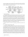
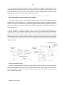
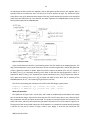
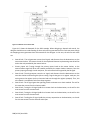
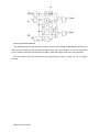
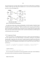
2.2 Uncle Flow Overview
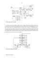
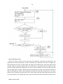
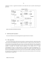
Figure 2-1 shows the Uncle tool flow. The flow is controlled by python scripts that invoke the various
tools in the flow. The input RTL is transformed to a gate level netlist using commercial synthesis tools
(both Synopsys Design Compiler and Cadence RTL Encounter are supported). The input Verilog RTL file
contains a mixture of behavioral and gate-level statements that describes a mixture of combinational
and control logic. The gate-level statements are necessary for instantiating elements that support the
RBR/V0.2.6/June 2013
7
asynchronous paradigm and which cannot be inferred from behavioral RTL statements. Parameterized
modules are available from an Uncle-provided library and are used to reduce the code footprint of these
constructs, reducing the RTL coding burden on the designer.
Figure 2-1 Uncle Synthesis Flow
The target library read by the commercial synthesis tool contains and2, xor2, or2, inverter, D-flip-flop
(DFF), D-latch (DLAT), and other gates that are either black boxes for special use (such as T-,S- elements,
discussed later), or are complex gates that have been mapped to an optimized NCL implementation (i.e.,
a full adder). These gates have unit delays for timing, and area figures that are relatively proportional to
their transistor counts. The single-rail netlist is then expanded to a dual-rail netlist with gates and
registers expanded to their actual dual-rail implementations. The ack network is then generated, at
which point the gate level netlist is simulation-ready. The steps after this point are optional
optimizations and checking. The ack checker is a tool that reverse engineers the ack network to
mechanically check its correctness. This is primarily included as a check for coding errors in the ack
generation tool when new approaches in ack network generation are tested.
The various components of this flow will be discussed in more detail in later sections of this
document.
2.3 Dual Rail Combinational Logic in NCL
The asynchronous methodology supported by Uncle is dual-rail, four-phase, with fine-grain gates.
The combinational logic in the single_rail_netlist.v file of Figure 2-1 contains basic two-input gates such
as AND2, OR2, XOR2, and INV which are expanded to their dual-rail versions implemented in NCL gates.
NCL is used instead of some other style such as DIMS as it produces logic with fewer transistors and
lower delays. For example, a dual-rail AND2 (DRAND2) requires 31 transistors implemented in NCL
versus 56 transistors in DIMS. Three-input (and higher) basic Boolean gates are not used as their dualrail expansions are generally not as efficient as the two-input versions ([7] has a good discussion on
dual-rail expansion of combinational logic to NCL). The combinational logic also has a few complex gates,
such the full-adder and mux2, that have direct NCL implementations that are far more efficient than by
representing these gates as primitive two-input gates and then dual-rail expanding these gates. These
complex cells are expanded to their NCL implementations during the flow of Figure 2-1. One of the
RBR/V0.2.6/June 2013
8
future goals of the Uncle toolset is to offer better logic synthesis in terms of direct NCL implementation
of complex gates rather than using primitive gates that are later expanded to dual-rail logic.
A note on the NCL full-adder cell
The NCL full-adder cell [4] is very efficient implementation in terms of transistor count and speed,
but it has the property that the carry-out (CO) is not input-complete (its t/f rails do not depend on all of
the t/f rails of the A, B, CI inputs). However, as long as the CO is used as the carry-input (CI) of another
full-adder cell, input completeness of the sum bits are preserved. This means that if you want to use the
most-significant carry-out of a ripple-chain, then you need to use XOR3 gating in order to have an input
complete output. Sometimes, the Synopsys/Cadence synthesis tools will use a full-adder cell as an XOR3
gate (only the CO output is used, the SUM output is unconnected). During the mapping process, Uncle
detects this condition and replaces the full-adder with a dual-rail XOR3.
2.4 Data-driven vs. Control-driven Design Styles
A complete digital system also needs registers and a sequencing mechanism in addition to
combinational logic. Uncle supports two distinct design styles for registers/control: data-driven and
control-driven (i.e., Balsa-style). These terms are more fully defined in the following sections, but some
guidelines on the usage of these styles are given here as this is a basic choice that a designer must make
before implementing their module (or sub-module within a larger design).
•
•
•
The data-driven style is the best choice in terms of performance for linear pipelines. For
transistor count/energy, the better choice (data-driven/control-driven) is design dependent.
The data-driven style is generally the best choice in terms of performance for a block that has
feedback (i.e. accumulators, finite state machine) if ALL registers, ALL ports are read/written
each compute cycle. This assumes that the block is performance-optimized using the automated
delay balancing tool available in the tool flow. If minimal energy/transistor count is required,
then the control-driven style is generally better.
The control-driven style is the better choice in terms of transistor count/energy for blocks that
have registers with conditional read/writes, and/or ports with conditional activity. It can also be
better in performance than the data-driven implementation, but it depends on the block.
Uncle supports designs that mix sub-modules that use different styles (the Viterbi example in the
$UNCLE/designs/ directory is an example of this). The data-driven style currently has more support in
the Uncle flow in terms of optimizations because the first version of Uncle only supported this style, but
it is envisioned that future versions of Uncle will also support a variety of optimizations for the controldriven style.
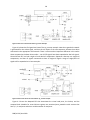
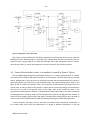
2.5 Data-driven Control and Registers
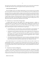
Figure 2-2a shows a data-driven dual-rail half-latch (the term half-latch is used because in a FIFO
arrangement, two of these are required for each bit stored in the FIFO). In this system, the acknowledge
signals ki, ko are at logic 1 when the data rails are at NULL. Because of this, an asynchronous reset signal
is required in the C-element to force its output to NULL during system reset. This is a reset-to-NULL halfRBR/V0.2.6/June 2013
9
latch as both outputs are reset to 0 during a system reset. In Uncle, a dual rail signal has t_/f_ prefixes
for true/false rails, respectively. The transistor level implementation of the half-latch used in Uncle is
somewhat different from that shown in Figure 2-2a in that it isolates the t_q/f_q output loads from ko
signal generation. It does this by using internal signals taken before the final inverter stage in the C-gates
as inputs to an AND2 gate that then drives the ko output load. This costs four more transistors (34
transistors versus 30 transistors for the design of Figure 2-2a) but produces a faster ko path when
t_q/f_q are loaded.
Figure 2-2 Data-driven Half-latch
Figure 2-2b shows how the acknowledge signals are used to control data transfer between two of
these half-latches in the familiar micro pipeline arrangement. The ackin (ki) of a bit in latch A is tied to
the output of a C-element completion tree whose inputs are the B-latch ackouts (ko) of all the
destinations of that bit. The data sequencing between bits in the registers is controlled by arrival of data
waves, NULL waves at the half-latch and by the ack network.
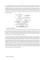
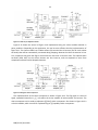
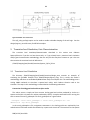
A finite state machine with feedback requires a different form of latch element. If the C-element of
Figure 2-2a that drives the t_q output is replaced with a C-element that resets to 1, then this becomes a
reset-to-DATA1 (drlats) half-latch (the latch outputs have a dual-rail DATA1 at system reset). Conversely,
a reset-to-DATA0 (drlatr) half-latch is formed by replacing the C-element driving the f_q output with a Celement that resets to 1. Figure 2-3 shows a finite state machine implementation with state registers
implemented as three half-latches, with the middle half-latch containing initial data. This forms a three
half-latch ring which is the minimum required for data cycling [4], and the initial data in the middle halflatch is required in order to insert a data token on this loop. This register type is expensive in terms of
transistors (and associated energy), requiring 3*34 = 102 transistors per bit. This register type is termed
a dual-rail data-driven register in this document.
RBR/V0.2.6/June 2013
10
Figure 2-3 Finite State Machine
This document refers to a system using this style of registers/control as data-driven, since there is no
separate control network other than the ack network. In this data-driven style, all ports and all registers
are read and written every compute cycle (port/register activity can be further restricted in a datadriven design, but requires extra effort in terms of additional gates; examples are given later in this
document).
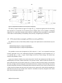
2.6 Control-driven Control and Registers
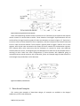
Conversely, this paper refers to a control-driven system as one that has registers with selective
read/writes and a control network that is separate from the datapath such as that implemented by
Balsa. Figure 2-4a shows a dual-rail register based on an SR-latch (this register has a low-true ko; Balsa
uses a register with high-true ko). Any number of read ports can be easily added to the register by
placing AND2 gates on the dual-rail outputs, with each port enabled by a single-rail control signal as
shown in Figure 2-4b. A write operation is triggered by data arrival, while a read is triggered by assertion
of the associated read line with a port. This provides a selective read/write control capability for the
register. With one readport, the register in Figure 2-4a requires only 28 transistors per bit, compared
with the 102 registers per bit of the register in Figure 2-3 or the 34 transistors per bit for the half-latch of
Figure 2-2a. Generally, control-driven designs will have lower transistor counts and lower energy than
data-driven designs. Note that the register of Figure 2-2a has no initialization capability; Uncle provides
reset-to-0 and reset-to-1 versions as well.
RBR/V0.2.6/June 2013
11
Figure 2-4 Dual-rail register based on an SR latch.
Balsa uses handshaking modules known as S-elements and T-elements [9] to implement the separate
control channel for control-driven transfers. These elements have elegant implementations that are
small and fast; the signal transition graphs for these two elements are shown in Figure 2-5. Typical use is
to connect a chain of these elements to form a sequencer, with the la output of one element connected
to the lr input of the next element. The Or output is typically used to trigger a read on one or more
registers, with the Oa input connected to the output of the ack network for the destination registers.
The T-element offers more concurrency than the S-element as it asserts la+ (starts next sequencer
element) when Oa+ occurs, thus beginning the next datapath action while the current datapath action is
returning to NULL. Balsa uses clever configurations of these elements with additional gating to
accomplish various control structures such a loop-while, if-else, etc. Example usage of these elements in
Uncle designs are provided later in this document.
Figure 2-5 S-element, T-element STGs.
3 Data-driven Examples
This section gives examples of data-driven designs; all examples are available in the designs/
subdirectory of the Uncle distribution.
RBR/V0.2.6/June 2013
12
3.1 RTL Constructs
All behavorial RTL examples in this document are given in Verilog. The native Uncle tools themselves
can only parse Verilog gate-level netlists (named port association only), and rely on a commercial
synthesis tool such Synopsys Design Compiler or Cadence RTL Compiler to synthesize behavioral RTL to
the gate-level netlist that enters the Uncle tool flow. You could also use VHDL as the initial RTL, as long
as the final gate netlist was in Verilog. Regression test examples in the Uncle toolset are all in Verilog
RTL, and the majority have been tested with both Synopsys and Cadence.
Combinational logic in Uncle designs are specified using standard Verilog constructs. For arithmetic
blocks, RTL operators such as ‘+’, ‘<’ etc. can be used, but Uncle examples often used parameterized
modules that directly instantiate complex gates such as a full-adder to give full control over the
structure used for the arithmetic operator instead of relying on the synthesis tool’s choice. An important
file in the Uncle distribution is:
$UNCLE/mapping/tech/models/verilog/src/gatelib/parm_modules.v
This file contains numerous parameterized macros that are used in several examples. This file is only
used for synthesis purposes, and is automatically read by the scripts used for Synopsys/Cadence
synthesis. We will point out the use of these macros as the examples are discussed.
Figure 3-1a shows how to infer a half-latch from a behavioral Verilog statement. The behavioral
Verilog generates a D-latch in the single-rail gate-level netlist, which is transformed during the mapping
process into a dual rail half latch (a drlatn cell, which is a reset-to-NULL half-latch). Note that a clock
signal needs to be present in the module’s interface in order to infer this latch; this signal is dropped
during the mapping process. Figure 3-1b shows how to infer a DATA0 register from a behavioral Verilog
statement. This infers a DFF (D-flip-flop) with a low-true reset in the single-rail gate-level netlist, which is
transformed to the three half-latch structure (data-driven register) during the mapping process. Note
that the middle latch is a reset-to-DATA0 half-latch. If the statement q<=0 is replaced with q<=1 then
the middle half-latch becomes a reset-to-DATA1 half-latch. If the always block of Figure 3-1b is modified
to drop the asynchronous reset, then the DFF that is generated in the single rail netlist will not have a
reset input. However, this DFF will still be mapped to the structure of Figure 3-1b during dual-rail
expansion and a default reset input added, as all data-driven registers are assumed to have initial data.
RBR/V0.2.6/June 2013
13
Figure 3-1 Data-driven half-latch/register inference from RTL.
3.2 RTL Restrictions
There are a few restrictions on the RTL that can be used for Uncle designs:
•
•
Clock signal: For the flattened top-level module, all input to output paths must go through at
least a half-latch; there can be no combinational-through paths. This also implies that in a datadriven design, the top-level design must have a clock signal in order to infer DFFs/D-latches. A
control-driven design does not require a clock signal as these registers are manually instantiated
by the user. There can be no gating logic on the clock signal.
Asynchronous reset: An asynchronous reset line is not required in a data-driven netlist but all
final NCL netlists will have one, so a low-true asynchronous reset with a default name is
generated if one is not specified. Control-driven RTL is required to have a low-true asynchronous
reset at the top-level module as one of the required gates needs this input. There can be no
gating other than buffers/inverters on the asynchronous reset, and the asynchronous reset can
only be used as the reset for DFFs or latches, and not in general logic. Buffering to meet a userspecified transition constraint is added to the asynchronous reset network during the mapping
process; this is discussed later.
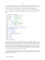
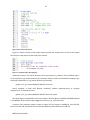
3.3 First example: clk_up_counter.v to ncl_up_counter.v walkthrough
The first example is clk_up_counter.v and is found in:
$UNCLE/designs/regress/syn/rtl/clk_up_counter.v
RBR/V0.2.6/June 2013
14
Uncle’s example directory structure uses the convention that commercial synthesis is done in the
syn/ directory, NCL netlist mapping in the map/ directory, and Verilog simulation in the sim/ directory.
For the rest of this example, many directory references are relative to $UNCLE/designs/regress/.
The Verilog code is shown in (this example was grabbed off the web from a popular Verilog tutorial
site). It is a standard up counter with an asynchronous low-true reset, and synchronous enable, clr
signals.
Figure 3-2 clk_up_counter.v RTL
The author’s naming conventions for examples tends to stray somewhat, but generally ‘clk_’,
‘clkspec_’ or no prefix is used on input RTL, with ‘ncl_’ or ‘uncle_’ prefix used for verilog files that result
from the mapping process. In this particular case, you can simulate this clocked RTL and you will get the
same inputs/outputs on a compute cycle basis as you will get from the mapped NCL netlist. So this is a
case where the input RTL can be simulated before mapping. However, for many other examples
(including all of the control-driven style examples), this will not be possible. The top-level module name
has to match the name of the input file without the .v extension.
To run the complete synthesis/mapping process for this example, execute the following command in
the $UNCLE/designs/regress directory (this assumes that Cadence RTL Encounter and the Cadence
Verilog simulator is on your path):
RBR/V0.2.6/June 2013
15
python doregress.py up_counter cadence default.ini -syntool cadence
This runs the complete flow including a regression test simulation. However, the design is typically
created in three major steps: a) RTL-to-single-rail netlist synthesis, b) single-rail netlist to NCL netlist
mapping, c) simulation of the NCL netlist. This corresponds to the syn/, map/, and sim/ subdirectories
under the $UNCLE/designs/regress directory. The rest of this section discusses how to run these
separate steps (more information on the regression script can be found in the appendix).
RTL Synthesis to gate-level single-rail netlist
To perform the RTL-to-single-rail netlist synthesis, change to the $UNCLE/designs/regress/syn
directory and execute the command:
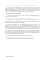
synrc_design.py default_cadence.template %TOP%=clk_up_counter
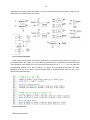
This synthesizes the syn/rtl/clk_up_counter.v file to a gate-level netlist stored in file
syn/andor2_rc/clk_up_counter.v using Cadence RTL Encounter. This file is shown in Figure 3-3; observe
that the combinational gates are primitive two-input gates.
The default_cadence.template file is a synthesis template script that synthesizes for a minimum area
constraint and is contained in the $UNCLE/mapping/tech/cadence directory. The
mindelay_cadence.template file synthesizes for a minimum delay constraint and may result in a faster
design for designs with complex combinational blocks (or it may not, since longest path delays in
asynchronous dual-rail netlists can be data-dependent, and furthermore, the gate-delays specified in the
.lib file used for synthesis only contains unit-delays. This is an area that needs further improvement). A
current limitation is that the mindelay_cadence.template file can only be used for data-driven designs
and not for control-driven designs because how the script is written to look for dff/Dlatch-to-dff/Dlatch
paths (this restriction will be removed in a future release).
Use the following command if you wish to use Synopsys dc_shell for synthesis:
syndc_design.py default_synopsys.template %TOP%=clk_up_counter
The resulting gate-level netlist is placed in the syn/andor2_dc/clk_up_counter.v file.
RBR/V0.2.6/June 2013
16
Figure 3-3 clk_up_counter.v single-rail netlist
Gate-level single-rail netlist to NCL netlist mapping
For NCL mapping, first copy the syn/andor2_rc/clk_up_counter.v netlist to the map/ directory. Then,
edit the clk_up_counter.v file and change the module name from clk_up_counter to ncl_up_counter.
This is needed as this module name is passed to the Uncle tool as the top-level module, and it also forms
the basis for the output file name. If you do many of these designs, you will probably write a script to
automate this step to your personal preferences (as is done automatically during the doregress.py
regression script). CHANGE version 2.6: With version 2.6 and later, it is no longer necessary to edit the
Verilog file and manually change the module name – the top module name of the Uncle Verilog file will
be the second argument passed on the Uncle command line.
Execute the following command in the map/ directory to map the netlist to an NCL netlist:
RBR/V0.2.6/June 2013
17
uncle clk_up_counter.v ncl_up_counter default.ini
After many lines of status output is produced, the NCL netlist is written to ncl_up_counter.v. The
uncle command is a python script that expects three arguments : 1) input file name, 2) top module
name, and 3) options file. The default.ini file is an options file the executes the default flow (see the
chapter on technology files for an explanation of some of the options in a .ini file, these reside in the
$UNCLE/mapping/tech directory). The only performance optimization in the default flow is a netbuffering step, that buffers heavily loaded nets to meet a global transition time constraint (see the netbuffering section later in this document). The only area optimization performed in the default flow is a
cell merging step that merges adjacent cells with no fanout to more complex gates.
During the mapping process, several intermediate netlists are produced in the tmp/ subdirectory.
Some of these files are (the entire tmp/ directory can be deleted after mapping if desired):
•
•
•
•
•
•
•
•
•
modname_dr0.v – after dual-rail expansion.
modname_dr1.v – after inverter removal (inverters are replaced by assignment statements that
swap the rails).
modname_dr2.v – after netlist flattening of dual-rail gates to threshold gates.
modname_safe0.v – after ack network generation. This is a complete NCL implementation, and
is a good file to use for detailed debugging as the DFFs have not yet been flattened to three halflatch implementations, and so there are fewer signals to deal with. Also, simulate this file if you
suspect a problem due to either relaxation or merging.
modname_safe1.v – DFFs flattened to half-latch implementations.
modname_nbuf0.v – the netlist after net buffering has been done.
modname_merge1.v – after gate merging – this can cause nets to be deleted.
modname_cleanup0.v – a cleaned up version of the netlist with dead gates removed. This is the
netlist that is used by the acknetwork checker that checks for structural correctness of the ack
network.
modname.v – This is the final netlist, and is written to the current directory. This netlist has
been cleaned of all verilog attributes that have been added during various stages of the
transformation process.
Files produced in the current working directory other than the final netlist of modname.v are:
• modname_stats.txt – netlist statistics at the various transformation stages (the only one that
you are generally interested in is the total_area statistic at the end of the file that is the total
number of transistors, and the output_cycle_average_time if the uncle_sim tool has been run).
• modname_acks.txt – information on the acknowledgement networks that are generated, useful
if your final netlist does not cycle and you are trying to debug it.
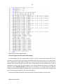
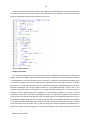
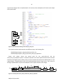
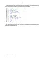
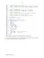
A portion of the ncl_up_counter.v netlist is shown in Figure 3-4. Note that the port names now have
‘t_’ and ‘f_’ as prefixes except for the asynchronous reset, and new ports named ackout, ackin have
been added. Any gates with cgateN instance names are part of the ack network. Any gates with instance
RBR/V0.2.6/June 2013
18
names of cmrg_N names have been merged by the cell merger. Any gates with instance names of
buffcomp_N names have been added during net buffering.
Figure 3-4 Part of ncl_up_counter.v
NCL netlist simulation using uncle_sim
Before using an external Verilog simulator to verify the netlist, you can use the internal Uncle
simulator to do some basic checking (this is done in the regression test). Execute the following command
line to apply random inputs for 100 output cycles:
uncle_sim ncl_up_counter.v default.ini -top ncl_up_counter -maxcycles 100
Stats given at the end of this simulation is (time is in picoseconds):
Finish time: 534076, Number of data output cycles: 100, Average output cycle
time: 5340, Transitions per cycle: 179, Switched capacitance per cycle:
3.658548e-13,
By default, the internal simulator reads NLDM characterization information from the file (this file
specified by an option in the default.ini file):
$UNCLE/mapping/tech/timing65nm.def
This timing characterization data was produced from pre-layout transistor-level gate models using
Cadence Ultrasim, with transistor models from a commercial 65nm process. Transistor-level simulations
using Cadence Ultrasim of the final NCL netlists have shown about a 5% agreement with predicted cycle
RBR/V0.2.6/June 2013
19
time. The Uncle simulator is an event-driven simulator that supports ‘0’, ‘1’, and ‘X’ values. The
simulator uses the function property in the Uncle cell definition files for evaluating generic Boolean and
NCL combinational gates. Special purpose gates such the mutex and various register cells have custom
models built into the simulator, with the ncl_func cell property used to identify the type of cell to the
simulator.
The Uncle simulator also reports three unusual/failure conditions (a waveform file named
module_name.vcd is produced by the simulator and can be viewed by the freely-available Linux tool
gtkwave to help debug these conditions):
•
•
•
•
Failure to cycle: An error is reported if the netlist fails to cycle. This can either be due to designer
error in the original RTL or because of incorrect netlist generation due to a tool error. See the
debugging chapter for hints on debugging dead netlists.
‘X’ values after reset: Unclesim holds reset asserted with primary inputs at NULL until the netlist
is settled, then releases reset and either applies random inputs or user-specified stimulus. An
error is reported and the simulator is exited if any ‘X’ (unknown) values are detected on gate
outputs once reset is settled. Check the .vcd waveform file to determine the cause of these ‘X’
nets.
Orphan or glitch detected: This is a warning, and means that a net transition that fanned out to
at least one NCL gate did not cause a corresponding transition in at least one of the fanout
gates. In general, the dual-rail expansion methodology used in Uncle does not cause gate
orphans in combinational logic, and the ack generation strives to not generate gate orphans.
Long chains of gate orphans may cause timing problems in NCL. It is possible that something the
designer has done using demux or merge gates can cause orphans. Orphans are an unusual
condition, and should be checked by the designer. The –ignore_orphan netname option can be
specified to the simulator to specifically ignore orphans that the design knows are ‘safe’.
Generally speaking, the netlists produced by Uncle should be orphan free. Obviously, the
orphan/glitch detection is only valid for the random vectors produced during the simulation run,
and does not guarantee that your design is orphan-free for all possible input vectors. Note:
some definitions of the term gate orphan use a timing constraint that do not report orphaned
signal transitions unless they have the potential to cause a logic error by persisting long enough
so that it collides with the next data wave. The Uncle simulator does not do any timing analysis
for the orphan/glitches that are reported.
Simultaneous assertion of dual-rail nets: This indicates that both rails of a dual-rail net have
been simultaneously asserted, and always indicates some serious error with the netlist. This
condition should never occur, and indicates either a tool error during the mapping process, or a
designer error in the original RTL. These should always be investigated.
The uncle simulator can also read external vector files instead of using random vectors; look at the
file:
$UNCLE/design/regress/map/gcdsimple.vecs
RBR/V0.2.6/June 2013
20
for an example of the input format, and the regression test labeled as gcdsimple_t2 in the
$UNCLE/design/regress/doregress.py file for command line options needed for uncle_sim. Because the
input vector format is a primitive one, it is best to have the external verilog simulator testbench produce
this file during its testing, as the following Verilog testbench does:
$UNCLE/design/regress/sim/src/uncle_gcdsimple/tb_uncle_gcdsimple.v
NCL netlist simulation using an external Verilog simulator
An external verilog simulator is required to fully test the NCL gate level design. The regression tests in
the distribution have Makefiles that are compatible with Synopsys, Cadence, and Mentor (modelsim)
simulators. The gate-level models are in $UNCLE/mapping/tech/models/verilog/src/gatelib and use unit
delays (the Uncle simulator with its NLDM timing model is intended for more accurate prediction of
netlist performance).
During mapping, a skeleton testbench file is also created named tb_modname.v (i.e.,
tb_ncl_up_counter.v). The testbench structure is shown in Figure 3-5. All input vectors are supplied as
single-rail vectors using the original single-rail port names via code placed in the initial process; a helper
process translates these to dual-rail signals. A helper task named ncl_clk is used to assert i_clk to apply
the data wave, waits for the falling edge of ackout that indicates the data wave was consumed, negates
i_clk to apply the null wave, and then waits for the rising edge of ackout that indicates the NCL block is
ready for new data.
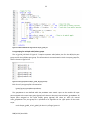
Figure 3-5 NCL Testbench structure
A snippet of Verilog testbench code for the initial process is shown in Figure 3-6. Lines 40-45 initialize
input signals and applies reset. Lines 49-53 is a loop that enables the counter, and then lets the counter
count for 511 data/null waves. Lines 53-56 disables the counters for a few data/null waves, and then
lines 57-58 clears the counter.
RBR/V0.2.6/June 2013
21
Figure 3-6 Part of the initial process.
Figure 3-7 shows a portion of the output capture process that captures the true rails of the output
once they are ready and prints the value to the console.
Figure 3-7 Testbench output capture/display.
Simulation is done in the sim/src directory. Once the map/ncl_up_counter.v file is produced, copy it
to the sim/src/ncl_up_counter directory (this directory already contains the fleshed-out testbench just
discussed). Compile the ncl_up_counter directory by executing:
gmake –f ncl_up_counter/Makefile TOOLSET=simchoice
where simchoice is either qhdl (Mentor modelsim), cadence (Cadence/ncsim) or synopsys
(Synopsys/vcs). To simulate, execute:
gmake –f ncl_up_counter/Makefile TOOLSET=simchoice dosim
The dosim target in the Makefile runs the simulation in batch mode for the default SIMTIME specified
in the Makefile, with simulator output logged to sim/src/ncl_up_counter/sim.log.
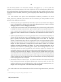
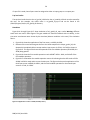
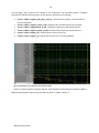
A portion of the simulator output is shown in Figure 3-8. The counter is enabled for lines 535-540,
held in lines 541-544, cleared 545-547 (clr takes precedence), and enabled in lines 548-551.
RBR/V0.2.6/June 2013
22
Figure 3-8 A portion of the simulator output.
3.4 Second Example: GCD16 (clkspec_gcdsimple.v)
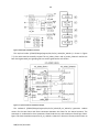
The file $UNCLE/designs/regress/syn/rtl/clkspec_gcdsimple.v implements the GCD algorithm shown
in Figure 3-9 using 16-bit values.
Figure 3-9 GCD using successive subtraction.
Two different regression tests are available in $UNCLE/designs/regress/doregress.py for this design
using the command lines shown below executed from the $UNCLE/designs/regress directory (these
command lines omit the synthesis step). The gcdsimple_t1 test runs Unclesim with random vectors,
while the gcdsimple_t2 runs runs Unclesim with a user specified vector file.
python doregress.py gcdsimple_t1 cadence default.ini
python doregress.py gcdsimple_t2 cadence default.ini
The datapath and finite state machine (FSM) for the gcdsimple example are shown Figure 3-10. There
is no attempt at power savings, all muxes are Boolean. The GCD block has the property that it should
only accept new input when it requires new input, which is during state S0. The rport box is a read port
module, and is used to control input port activity to meet this requirement. Similary, the DOUT output
port should only be active when output value is ready, which is during state S2. The wport box is a write
port module, and is used to control output port activity in this manner. In a data-driven design, having
RBR/V0.2.6/June 2013
23
conditional port activity costs extra gates in terms of read port/write port wrappers. These will be
explained in more detail later in this section.
Figure 3-10 GCD Datapath/FSM.
Code excerpts will be shown from clkspec_gcdsimple.v to illustrate how the elements of Figure 3-10
are implemented in RTL. Figure 3-11 shows RTL that implements the computational and mux elements
of the datapath. Even though you can use arithmetic operators such as ‘<’, ‘==’, ‘-‘, etc., this code uses
parameterized modules from parm_modules.v to ensure user-controlled architectures for these
operations. The use of the mux2_n parameterized module is important as the mux2 cell has a very
efficient NCL implementation.
Figure 3-11 Datapath RTL.
RBR/V0.2.6/June 2013
24
Figure 3-12 shows the RTL that implements the registers and FSM logic; this is written in essentially
the same manner as for a clocked system. State S0 activates the read port, state S1 performs the
iterative computation, and state S2 activates the write port.
Figure 3-12 Register/FSM RTL.
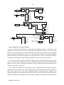
Read port operation
The rport box of Figure 3-10 is a read port, and is used to conditionally provide data to a data-driven
design. A data-driven design requires data/null waves every compute cycle, and the read port’s function
is to provide data from an external port when its read line is asserted, and provides dummy data when
its read line is negated. Figure 3-13a shows the RTL implementation of the read port macro. The input
port goes to a D-latch, whose output goes to a black-box component named demux2_half1_noack. A
black-box component has no logic function defined in the Cadence/Synopsys .lib file, and so the
synthesis tool simply keeps it unchanged in the netlist. Black-box components in Uncle are used to
implement either special gating that implements an asynchronous capability, or serves as virtual
annotation in the netlist that causes the mapping process to manipulate this portion of the netlist in
some manner. The output of the demux2_half1_noack gate goes to a merge gate, whose other input is
from a demux2_half0_noack gate that is fed by a constant 0 (this is the dummy data when the readport
is not selected). Both noack gates have select lines; one can view the half1_noack output as having
active data when its select input is logic 1, and the half0_noack output as having active data when its
select line is logic 0. The merge gate is also a black box component, that maps in the dual rail netlist to
RBR/V0.2.6/June 2013
25
an OR2 gate that ORs the false rails together, and an OR2 gate that ORs the true rails together (this is
typically called an asynchronous mux, and only one of the true/false rail pairs are assumed to have
active data in any cycle). Note that select inputs of the half_noack components is tied to a line named rd
(read) from the FSM; when rd=1 the external port data is gated to the FSM/datapath, when rd=0 the
dummy data is gated to the FSM/datapath.
Figure 3-13 Read port details.
Figure 3-13b shows how the RTL is translated to gates in the final netlist by the mapping process. The
half_noack components act as virtual instructions to the ack network generator, and the ack generator
creates a gated ack network as shown. Note the ki (ackin) input to the drlatn cell is only a ‘1’ (requestfor-data) if rd=1 (t_rd is asserted). Similarly, the ki input to the dual-rail logic 0 generator is only a ‘1’
(request-for-data) if rd=0 (f_rd is asserted). The C-gates connected to the t_rd/f_rd signals are reset-tonull C-gates since during reset, the t_rd/f_rd signals will both be null, while the ko (ackout) of the
FSM/datapath will be a ‘1’, thus requiring a C-gate with a reset line.
The RTL for instantiating the read ports in the RTL for the GCD design is given below:
readport_n
readport_n
#(.WIDTH(16)) rp_x (.clk(clk),.d(a),.q(ad), .rd(rd));
#(.WIDTH(16)) rp_y (.clk(clk),.d(b),.q(bd), .rd(rd));
Write port operation
The wport box of Figure 3-10 is a write port, and is used to conditionally provide data to the output
port of data-driven design. Figure 3-14a shows that the RTL view of a write port is just a demux2 blackbox component with the y0 output unconnected. The y0 port of a demux2 copies the input data if the
select line is false, and the y1 port copies the input data if the select line is true as shown in Figure 3-14c.
The purpose of the unconnected output port of the demux2 is to consume the output data by providing
a self-ack for this port as shown in Figure 3-14b. If your design is such that you know that the
RBR/V0.2.6/June 2013
26
FSM/datapath output will always be consumed by some destination (that is, an ack will be provided),
then the demux2 component can be replaced by a demux2_half1 component that only implements the
y1 output (this saves the cost of the self-ack gating).
Figure 3-14 Write port details.
The RTL for instantiating the read ports in the RTL for the GCD design is given below:
writeport_n
#(.WIDTH(16)) wp0 (.d(bq),.q(dout), .wr(wr));
4 Control-driven Examples
This section gives examples of control-driven designs; all examples are available in the designs/
subdirectory of the Uncle distribution. The control-driven design methodology is taken from the Balsa
synthesis toolset by examination of the Balsa generated netlists and through published articles on Balsa
control; the author’s contribution is to make this methodology available in a Verilog RTL form and to
provide some optimizations to it such as C-gate sharing in ack networks.
4.1 First control-driven example: up_counter.v to ncl_up_counter.v
The first control-driven example is up_counter.v and is found in:
$UNCLE/designs/regress_dreg/syn/rtl/up_counter.v
The regression test for this example can be run in the $UNCLE/designs/regress_dreg/ directory using
the command:
python doregress.py up_counter cadence default.ini -syntool cadence
RBR/V0.2.6/June 2013
27
Control-driven designs requires more designer effort at the RTL level than data-driven designs, as
each register in data driven RTL (a DFF) most probably needs to be split into master/slave latches in the
control-driven RTL, with each latch accessed in a different state of the control-driven sequencer. The
control logic has to be instantiated manually as a network of S/T elements. There are some modules in
the parm_modules.v file that can somewhat reduce the RTL overhead of specifying a control-driven
sequencer; these will be discussed when encountered in example designs.
Figure 4-1 shows the RTL view of the control-driven up_counter example. The register is
implemented as separate master, slave latches that are controlled by a two-state sequencer. State S0
gates the external inputs, reads the slave register, and updates the master register with the new counter
value base on the slave register value and the external inputs. State S1 writes the slave register, and
places the counter value on the out terminals. The vrport black box component is a virtual read port
(module name is vreadport) used by control-driven designs for conditional access of external inputs. It
differs from the read port module previously discussed in that it does not provide dummy values when
its select line is false, and it does not actually contain a register. It serves as a virtual instruction to the
ack network generator and causes a gated ack network to be placed on the ackout primary output in the
final netlist (see Figure 4-2).
The two-state sequencer is implemented using three modules from parm_modules.v: loopen,
seqelem_kib, and seqdum_kib. The loopen component implements the logic shown, and is used to form
a repeated sequence of actions. State S0 is implemented with the seqelem_kib component (an Selement), with the terminals of Figure 2-5 renamed as start == lr, y == Or, kib == Oa (+ inverter), done ==
la. The kib terminal is typically tied to the auto-generated ack network. The letter b in kib is used to
indicate that this comes from a low-true ack network such as generated by the data registers, and has to
be inverted inside of the seqelem_kib component (there is also available a seqelem component that
expects a high-true ack, and has a terminal named ki). In the RTL, the kib terminal is tied to logic ‘0’ as
Uncle expects all inputs to components in the starting netlist to be connected; during the mapping
process this is replaced by the auto-generated ack network. Typically, ackin/ackout terminals are not
exposed on black-box modules used in RTL, but they are in the case of S/T-elements as there is a need to
manually connect these in some cases (to be discussed later). The seqdum_kib is simply wires and one
inverter as shown Figure 4-1; the last S/T element in a loop can be replaced by wires instead of using
gating.
RBR/V0.2.6/June 2013
28
Figure 4-1 RTL view of the control-driven up_counter example.
Figure 4-2 shows the final gate-level view of the up_counter example. Note that a gated ack network
is generated for the ackout signal, and that the ack inputs of the two sequencer elements have been
connected to the appropriate ack networks. There is also one other important difference in this netlist
when compared to the data-driven netlist – not all RTL signals have been expanded to dual-rail signals.
Control-driven RTL has both single-rail and dual-rail components. Sequencer elements are single-rail
components, and thus all signals connected to them all single-rail signals. Usage of single/dual rail
signals will be expanded on in later examples.
Figure 4-2 Gate-level view of the control-driven up_counter example.
Figure 4-3 shows the datapath RTL that instantiates the virtual read ports, the latches, and the
compute block. Modules for control-driven registers are contained parm_modules.v with versions that
have 1, 2, 3 read ports and also a variable number of read ports.
RBR/V0.2.6/June 2013
29
Figure 4-3 Datapath RTL for up_counter example.
Figure 4-4 shows the RTL that implements the sequencer; this is a straight-forward instantiation of
the logic shown in Figure 4-1.
Figure 4-4 Control RTL for up_counter example.
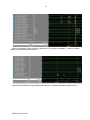
Figure 4-5 shows a simulation for the final netlist. Because synthesis does not always preserve net
names used in the RTL, the mapping of gate-level net names to RTL names is given at the top of the
timing simulation. This simulation uses the same test bench as used for the data-driven up counter
example, which is as it should be, as data-driven versus control-driven should not change the module’s
interface. The time marked as point A shows the ack assertion (after the internal inverter in the
seqelement_kib component) in response to the S0 assertion; note that this causes S0 to be negated,
which then triggers the ack negation. Observe that s1_start assertion occurs after the S0 ack is negated.
RBR/V0.2.6/June 2013
30
Figure 4-5 Timing for up_counter done using Balsa style components (uses an S-element).
Figure 4-6 shows a simulation for the up counter in which the S-element has been replaced with a Telement (this example can be found in $UNCLE/designs/regress/syn/rtl/clk_up_counterv2.v). Observe
that the s1_start assertion is now triggered by the S0 ack assertion and not by its negation. This overlaps
the return-to-null action of S0 with the data wave of S1, resulting in a faster cycle time.
Figure 4-6 Timing for up_counter done using Balsa style components (uses a T-element).
4.2 While-loops, choice
The previous example had a two-state sequencer with no conditional execution. Figure 4-7 shows a
sequencer with a while-loop. State S0 reads external ports, followed by states in the dotted box that
compute a flag, then test flag the flag, with states S1, S2 executed if the flag test is true. State S3 is
executed on loop exit, which returns back to S0 on completion.
RBR/V0.2.6/June 2013
31
Figure 4-7 Sequencer with while loop.
Figure 4-8 gives the RTL view of the control for the sequencer of Figure 4-7. The key component is
the whileloop2step component, which is a module that is available in parm_modules.v. The
whileloop2step module first computes the flag that is used to control the loop execution, then
reads/test the flag, and conditionally executes the loop body. All of the signals connected to the
whileloop2 module are single-rail signals, except for the flag signal, which is dual-rail. It is assumed that
the compute_flag signal is used to compute the flag that is written to a single bit latch, whose read port
is connected to the rd_flag signal, and whose output is connected to the flag input. The tseqelem
components are just place holders and can be replaced by S/T elements as desired.
Figure 4-8 RTL view of control for sequencer with while loop.
Figure 4-9 gives the whileloop2step module implementation details. A seqelem component is used to
control a two-state sequencer that implements the compute flag and read flag steps. The drexpand
module is a black box component that is used to access the individual t_/f_ rails of a dual-rail signal at
the RTL level. The input to a drexpand component is a dual-rail signal, while the two output signals are
both single rail, making them suitable for connection to sequencer component inputs. Observe that the
f_flag signal is connected to the ki input of the seqelem component. This is an example of requiring a
control element with a non-inverted ki input, and also a case where the designer provides the net
RBR/V0.2.6/June 2013
32
connection for the ki input instead being connected during the mapping process to an ack network. In
terms of operation the two-state sequencer remains operational as long as the t_flag signal is asserted
during the flag read state.
Figure 4-9 whileloop2step module details.
An optimization can be applied to this while loop if the while body only has one state. This implies
that the while-body will be implemented with a wired-sequential element, a seqdum component, which
also means that the last tseqelem element of Figure 4-9 can be replaced with a seqdum component as
well.
Figure 4-10 shows a sequencer with choice. State S2 is executed if the flag is false, else State S3 is
executed.
S0
Write flag
S1
S2
0
flag
1
S3
Figure 4-10 Sequencer with choice.
Figure 4-12 shows one method of implementing the control of Figure 4-10 using sequencer elements.
Sequencer element U1 implements state S0 (writes the flag), while element U2 implements state S1
(reads the flag). The t_/f_ rails of the flag are used to trigger sequencer elements that control states
S3/S2 respectively. The sror2 black-box component is a single-rail OR2; since only one sequencer
element (U3 or U4) is activated, this gate combines the done signals of these two components to a
single done signal that is then used as the ack for sequencer element U2.
RBR/V0.2.6/June 2013
33
Figure 4-11 One way to implement choice.
Figure 4-12 shows the control of Figure 4-10 implemented using the choice module available in
parm_modules.v. Depending on the application, this can be more efficient than the implementation of
Figure 4-11. The choice module has a hidden ackout (ko) terminal that is low-true (like all Uncle ackout
terminals) that will be automatically connected during mapping. Because the choice ko terminal is lowtrue, sequencer that gates the flag to choice element must have a low-true ackin. The exposed ackin
terminals (kib0, kib1) on the choice element are also low-true, and are expected to come from
completion networks tied to datapath elements.
Figure 4-12 Using the choice component.
The implementation of the choice component is shown in Figure 4-13. The flag signal is a dual-rail
signal, expanded internally to t_/f_ rails within the choice module. All ackins/ackout are low-true. The
choice component can be used to implement if{}/else{} within a sequencer. Also shown in Figure 4-13 is
a choice1 module, which is useful for implementing an if{} capability within a sequencer.
RBR/V0.2.6/June 2013
34
Figure 4-13 Implementation details for the choice/choice1 components.
The ability to expand a dual-rail signal to its single rail t_/f_ component signals at the RTL level along
with exposure of all terminals of S/T elements gives a designer quite a bit of freedom in designing
sequencers for control-driven designs. Other single-rail components that are available for instantiation
in RTL code are srand2 (AND2), srnor2 (NOR2), srinv (inverter), and cgate2/3/4 (C-elements).
4.3 GCD control-driven example: gcd16bit.v to uncle_gcd16bit.v
Two different versions of the GCD16 problem of Figure 3-9 implemented in control-driven style are
found in:
$UNCLE/designs/regress_dreg/syn/rtl/gcd16bit.v
$UNCLE/designs/regress_dreg/syn/rtl/gcd16bitfast.v
The gcd16bit.v version uses the approach in [10] in that the ‘==’ and ‘>’ are computed in each loop
iteration, with either ‘a-b’ or ‘b-a’ conditionally computed. The gcd16bitfast.v version computes ‘a-b’, ‘ba’ in parallel with ‘==’ and ‘>’ to get a faster design at the cost of more energy. This section only
discusses the gcd16bit.v version.
Figure 4-14 shows the FSM for the control-driven GCD. The RTL that implements this FSM uses the
whileloop2step and choice modules discussed in the previous section. State S0 reads the external a, b
ports and writes these to the master latches for a, b. State S1 reads the master latches, and computes
the a!=b, a>b flags as well as writing the slave latches with these a, b values. If the a!=b flag is true, then
the while loop body is executed. The loop body either executes state S3 (if a>b is true) or state S3 (if a>b
is false). State S3 computes a-b and writes the result to the a master latch, while state S4 computes b-a
and writes the result to the b master latch. State S5 is executed on loop exit, and gates the b master
latch value to the external dout port.
RBR/V0.2.6/June 2013
35
Figure 4-14 FSM for control-driven GCD.
Figure 4-15 shows the datapath for the GCD example. When designing a datpath and control, the
designer should have an understanding of where acks will be generated from for each state even though
the mapping process generates those ack networks for the designer. In this case, the acks for each state
are:
•
•
•
•
•
•
•
State S0 ack: The ack generator traces the s0 signal, and discovers that the destinations are the
two master latches. This means the ack for the sequential element implementing state S0 will be
tied to the acks provided by the master latches.
Primary inputs ack: Tracing through the primary inputs leads to the master latches, so the
external ackout signal will be an ack network provide by the master latches. However, since the
primary inputs go through virtual read ports, this ack network will be gated by the S0 signal.
State S1 ack: The ack generator traces the s1 signal, and discovers that the destinations are the
two slave latches and two flag bits (when tracing a signal that goes to a register read port, the
tracing enters the register via the rd terminal and exits through the register q output). Thus, this
ack network is composed of acks from those registers.
State S2 ack: The s2 signal gates the agtb flag, which terminates on a choice module. The ack for
this state then comes from the choice module.
State S3 ack: Tracing the S3 signal yields the a master latch as the destination, so the ack for this
state comes from the a master latch.
State S4 ack: Tracing the S4 signal yields the b master latch as the destination, so the ack for this
state comes from the b master latch.
State S5 ack: Tracking the S5 signal yields the primary output dout as the destination, so the ack
for this state comes from the external ackin input.
RBR/V0.2.6/June 2013
36
Figure 4-15 Datapath for control-driven GCD.
The transistor level simulation for this design compared to the fastest data-driven version (used net
buffering and latch balancing which is discussed later) showed about the same performance, but the
transistor count, energy usage for the data-driven designs were 2.8X, 4.9X greater than the controldriven design. Clearly, a control-driven approach is the best choice for this particular problem.
4.4 Control-driven divider circuit – two methods (contrib. by Ryan A. Taylor)
The file $UNCLE/designs/regress/syn/rtl/clkspec_div32_16.v is a simple implementation of a divider
circuit with a 32-bit dividend, dd, and a 16-bit divisor, dv. The outputs are 16-bits wide and are named qt
and rm, appropriately. There also exists one asynchronous active-low reset signal named reset. Shown in
Figure 4-16, below, is the FSM for the original clocked design. The relevant Verilog code is shown in this
figure as well. The FSM is not complex. It has only one decision, and that decision only loops back to the
current state. In order to optimize this code for a control-driven asynchronous design, some alterations
will have to be made to the general layout of the FSM. State s0 will remain the same in the
asynchronous implementation. However, a whileloop2step element will need to be used to implement
the looping decision. Therefore, state s1 will be implemented as a part of the flag generation network to
make use of the compute_flag and read_flag signals. The body of this looping element won’t be used, so
states s2 and s3 will be implemented as states immediately following the whileloop2step element.
It can be noticed in the code in state s1 that there are multiple if-then statements. Traditionally, in
the clocked world, these could be implemented in a design as Boolean multiplexors. In the two
RBR/V0.2.6/June 2013
37
asynchronous designs that are implemented in this section, these multiplexors will be the main subject
of the optimization.
s0
s1
s2
s3
Figure 4-16 FSM and relevant Verilog code for clkspec_div32_16.v.
This system has been implemented in two different ways in the following files.
$UNCLE/designs/regress_dreg/syn/rtl/uncle_div32_16.v
$UNCLE/designs/regress_dreg_syn/rtl/uncle_div32_16_lowpower.v
Figure 4-17, below, shows the control path for the uncle_div32_16 and the
uncle_div32_16_lowpower systems. It should be noticed in this control path that there exists one fewer
state than the original system, clkspec_div32_16. This is because the state that is labeled state s1 in the
original design is implemented as a part of the whileloop2step element’s flag circuitry. The circuitry for
the flag is implemented as a part of the datapath in both systems because of this usage.
flag
s0
0
reset
en
a
y
loopen
y
kib
start done
tseqelem_kib
0
compute_flag
start
rd_flag flag body_start body_done
done
whileloop2step
compute_flag_kib
Figure 4-17 Control path for uncle_div32_16 and uncle_div32_16_lowpower.
RBR/V0.2.6/June 2013
s2
s1
0
0
y
kib
start done
y
kib
start done
seqdum_kib
seqdum_kib
38
The datapath for the uncle_div32_16 is shown below, in Figure 4-18. There are multiple items that
should be specially noted in this design that may be of interest to the reader. First, the element
srtodrconst1 is an element that expands a single-rail logic signal into a dual-rail logic signal. In the case of
this system, the signals kreg and cbit must be initialized to values of 1 and 0, respectively, upon system
reset. If these signals are driven by constant values, the ack network will fail to generate properly. For
similar reasoning as the justification for the vrport elements on the main inputs to the system, a
srtodrconst1 element must be used to generate inputs for constant values. For full disclosure, note that
the output of this element is concatenated to a 4-bit value before entering the merge gate in the kreg
branch of the system. Secondly, the reader should note the use of two multiplexors to generate the
signals to be used as the signal diff in the clkspec_div32_16 design. Based on the value of cbit, and the
current state, the signal diff, and diff_s1, will be calculated differently. This means that both inputs to
the multiplexors, which include at least three 16-bit adder/subtractors, will be in use each cycle, even
though only one of these branches is necessary. This will push the power budget far beyond the
required limits for this application. This issue is rectified in the uncle_div32_16_lowpower version of the
system.
kreg_slave
kreg_master
s0
kreg
merge2
srtodrconst1
d
q
dreg
rd
d
-1
compute_flag
q
dreg
rd
rd_flag
dvreg_master
dvreg
compute_flag
q0
rd0
dreg q1
rd1
d
s0
dvreg2
s1
ireg_master
dd
vrport
merge2
s0
q0
rd0
dreg q1
rd1
d
flag_slave
== 0
ireg[31:15] - dvreg
ireg[31:15] + dvreg
ireg
compute_flag
d
q
dreg
rd
0
1
flag
rd_flag
Compute
vrport
merge2
diff
ireg2[31:16] + dvreg2
diff
0
1
diff_s1
cbit_slave
cbit_master
srtodrconst1
merge2
Figure 4-18 Datapath for uncle_div32_16.
RBR/V0.2.6/June 2013
d
q
dreg
rd
rd_flag
cbit
cbit_s1
s0
ireg_slave1
ireg2
s1
Compute
dv
d
q
dreg
rd
diff[16]
cbit
compute_flag
d
q
dreg
rd
rd_flag
ireg_slave2
d
q
dreg
rd
dout
s2
39
kreg_slave
kreg_master
s0
srtodrconst1
kreg
merge2
d
q
dreg
rd
-1
d
compute_flag
q
dreg
rd
rd_flag
dvreg_master
dv
merge2
vrport
dvreg
cbit_f
dvreg2
q0
rd0
dreg q1
rd1
q2
rd2
d
s0
flag_slave
d
== 0
cbit_t
dvreg3
cbit_s1_t
q
dreg
rd
cbit_master
flag
rd_flag
cbit_slave
cbit
s0
merge2
srtodrconst1
q0
rd0
dreg q1
rd1
d
diff[16]
q
dreg
rd
rd_flag
drexpand
t_y
a
f_y
cbit_t
d
compute_flag
s1
cbit_s1
drexpand
t_y
a
f_y
ireg1[31:15] – dvreg2
ireg2[31:16] + dvreg2
ireg_master
dd
vrport
merge2
s0
q0
rd0
dreg q1
rd1
q2
rd2
d
ireg
cbit_f
ireg2
{diff_cbit_s1_t[15:0],ireg3[15:0]}
ireg_cbit_s1_f
cbit_t
ireg1[31:15] - dvreg
ireg2[31:15] + dvreg
ireg3
cbit_s1_t
cbit_f
cbit_s1_t
cbit_s1_f
ireg_slave
merge2
merge2
merge2
merge2
diff
q0
rd0
dreg q1
rd1
q2
rd2
d
rd_flag
dout
s2
ireg_cbit_s1_f
cbit_s1_f
Figure 4-19 Datapath for uncle_div32_16_lowpower.
Figure 4-19 shows the datapath for the uncle_div32_16_lowpower version of the design. A few
differences can be found. It can first be noticed that the srtodrconst1 element is used in the same
fashion as in the uncle_div32_16 version fo the design. The kreg branch of the design is left unchanged
from the previous implementation. Then, it can be easily seen that there are several differences
between the two systems shown in Figures 4-17 and 4-18. However, they are all related to alleviating
the problem stemming from using the two diff multiplexors causes: a major overuse of power.
For the cbit branch of the system, some minor changes are made that will affect the remainder of the
system in a large way. The signals cbit and cbit_s1 are fed into two elements of type drexpand. These
signals now have a signal_t component signal and a signal_f component signal. These signals will be
used in the remainder of the system.
For the dvreg and ireg branches of the design, the master dreg elements are no longer triggered by
compute_flag or state signals; they are now triggered by the dual-rail expanded component signals of
cbit_f, cbit_t, and cbit_s1_f. Since these component signals are generated with a trigger of the
compute_flag signal, the same general order of events occurs. Since the system now has three versions
of both the dvreg and the ireg signals, there is no longer a need for any multiplexors in the design. Only
RBR/V0.2.6/June 2013
40
one of the four branches of the merge network will be active, thus saving exponential amounts of power
on each cycle of the system.
Using a specified known set of 100 vectors, both of these versions of the divider system were
simulated using the uncle_sim package. The original version, uncle_div32_16, clocked at 15593
transitions per cycle and measured an average switching capacitance of 25.6 pF. The reduced-power
version, uncle_div32_16_lowpower, clocked at 14347 transitions per cycle and measured an average
switching capacitance of 18.34991 pF. The reduced-power version of this design, therefore, measured
an improvement of 1246 transitions per cycle (8% improvement) and 7.12 pV (28% improvement) over
the original design.
From this data, it is apparent that the goal of these control-driven designs should be to design in such
a way as to only have necessary logic working at any given time. If it is possible to design in such a way
as to add more transistors, but decrease the use of a large percentage of transistors at a time, then it
should be designed that way.
5 Optimizations
This section discusses the various area and performance optimizations available in the Uncle flow.
5.1 Net Buffering
Net buffering is a performance optimization step that reads an external timing data file for the target
library, where the timing data is non-linear delay model (NLDM) lookup tables for output transition time
and propagation delay based on input transition time and output capacitive load (the timing data file
also contains pin capacitance information). The cell library contained in the distribution has pre-layout
transistor-level spice sub-circuits that were characterized using Cadence Ultrasim using two sets of
transistor models, 65nm Berkeley PTC models and models from a commercial 65nm process. This timing
data is found in the files $UNCLE/mapping/tech/timing65nmptc.def, timing65nm.def respectively. The
following statements in the $UNCLE/mapping/tech/common.ini file selects the timing data file and delay
model used by net buffering and by the internal Uncle simulator:
delay_timingfile timing65nm.def
delay_timing_model nldm
The current net buffering implementation is a simple approach that buffers nets to meet a userspecified transition time (two different times can be specified; one for the global reset net and a default
one for all other signal nets). The following statements in the $UNCLE/mapping/tech/common.ini file set
these constraints (time units are picoseconds):
delay_max_transition_time 100.0e-12 #max transition time for signal nets
delay_max_transition_time_reset 200.0e-12 #max tran. time for reset net
RBR/V0.2.6/June 2013
41
The signal net target transition time shown above is approximately equivalent to a 1X inverter driving
four separate 4X inverter loads. During net buffering, if a transition time failure is found, then the
algorithm first tries to replace it with the smallest gate size (if multiple gate sizes are available for the
problem gate) that meets the transition time target. If gate variants are not available, then a buffer tree
using inverters is built. The target library has four drive-strength variants of inverters, three variants of
AND2, two variants of reset-to-NULL data registers, and two variants of the most commonly used NCL
gates. The net buffering is unsophisticated in that it does not buffer for performance by tracing critical
loops. However, for many designs this approach does improve performance, but slowdowns were noted
for a few designs in the Uncle regression suite. Simulations indicate that the NLDM delay engine in Uncle
produces results that are typically within 5% of the transistor level simulations using the pre-layout
transistor models. For silicon fabrication purposes, the NLDM characterization should be for library cells
with parasitics extracted from cell geometry for more accurate timing.
Net buffering can disabled via the following line in $UNCLE/mapping/tech/common.ini (the default
common.ini file has net buffering enabled):
netbuf_enable 0
5.2 Latch Balancing
#non-zero to enable
Latch balancing is a performance optimization for the data-driven style that moves half-latches in the
netlist to balance data delays with ack delays (for the remainder of this section, half-latches are simply
referred to as latches). In a linear multi-stage pipeline, the stage with the longest delay loop formed by
the forward data path and the backwards ack path sets the pipeline’s maximum throughput. In the datadriven finite state machine arrangement of Figure 2-3, the longest loop delay is formed by delay through
the combination logic plus the backwards delay path of the ack network. Figure 5-1a shows a datadriven FSM with an unbalanced delay where the data delay is approximately 2X that of the ack delay
(the length of the delay boxes indicates relative delay). The ack delay is dependent on the number of
destination points that sets the completion network depth, while the data delay depends on the data
logic complexity. Figure 5-1b shows the design after delay balancing in which logic has been pushed
through the L3 latches to reside between the L3 and L2 latches. Observe that the maximum loop delay
has now decreased. Additional speed up could possibly be obtained by also pushing logic between
latches L2 and L1, but the initial data on the L2 latches would then mean that the NCL logic between L2
and L1 would be in an unknown state. This could be solved by forcing the outputs of L2 low (but keep
the internal state high) or by adding resets to the affected NCL logic. Latch balancing generally results in
more transistors as the datapath width increases moving towards the source registers requiring more
latches, with a corresponding increase in the ack network size.
RBR/V0.2.6/June 2013
42
Figure 5-1 Latch Balancing.
The latch balancing algorithm as currently implemented in Uncle supports latch pushing as shown in
Figure 5-1 as well as latch pushing in linear pipelines. The latch balancing algorithm is an iterative
heuristic algorithm that proceeds as follows:
1. Find the longest cycle from every latch output to a destination latch back to its ack input with
the constraint that the data delay is larger than the ack delay (data delay, ack delay are kept as separate
components). Ignore cycles that terminate or originate on latches with initial data, or latches that
terminate on primary outputs (the policy should either not push latches with primary inputs as sources,
or primary outputs as destinations, in order to avoid additive delays when separate blocks are joined.
Uncle chooses to ignore latches that source primary outputs).
2. Separate the latches identified in step 1 into sets that share common destinations, and within
each set sorted by longest cycle. Once the individual cycles in each set are sorted, sort the sets by the
longest cycle of each set. Starting with the set with the longest cycle, discover what other sets are
destinations of this set, and remove them from the set list (we do not want to push logic into one set,
only to have it pushed out again to a different set in the same iteration, resulting in thrashing). Continue
this pruning process until there are no sets left to consider. The sets that are left have the property that
no sets have destination latches that are source latches in any of the remaining sets.
3. For each set left from step 2, consider each cycle and determine if the destination latch of the
cycle is a valid push candidate as per the criteria of Figure 5-2a (if accepted, LATj is pushed towards
LATi). If the latch is a valid push candidate, then add it to a list. Once all cycles in the set have been
considered, this list contains a list of latches from this set to push, and are sorted by decreasing cycle
time. Keep only the first k % percent of the latches on this list to push, where k is a user specified
RBR/V0.2.6/June 2013
43
variable (higher k values decrease iterations with a possible decrease in quality, the examples in this
paper used k=30%). Add these latches to the final push list.
4. The result of step #3 is a list of latches from all sets to push. The ack network is stripped and all
of these latches are pushed by one gate level. The ack network is regenerated, and net buffering (if
enabled) is redone and delays are propagated through the netlist. The algorithm then loops back to step
1. The algorithm terminates when step #3 fails to find any valid latches to push.
Figure 5-2 Latch Criteria.
An iterative algorithm is used instead of trying to push latches into multiple gate levels in one step
because of the difficulty in predicting delays in the regenerated ack networks. This algorithm works
appropriately for data-driven FSMs but has a problem with linear pipelines in that latches are pushed in
one direction only. The algorithm will fail to find any latches to balance if the linear pipeline has a
longest cycle delay as shown in Figure 5-2b as the destination of the longest cycle terminates on latches
that source primary outputs (in this case, LATj would need to pushed towards LATk). A workaround for
this case is for the designer to place another half-latch stage on the output. The algorithm also does not
automatically insert latch stages to meet a performance target; it works only with existing latch stages.
These shortcomings will be addressed in future tool revisions.
Latch balancing options
The Uncle options file perfopt.ini in the $UNCLE/mapping/tech/ directory can be used to enable the
latch balancing optimization. If run on a netlist with no half-latch to half-latch paths, then no latch
balancing is performed. The following options affect latch balancing (default values are shown):
balance_latch_push_percentage
0.30
balance_latch_improvement_fail_limit
RBR/V0.2.6/June 2013
10
44
The balance_latch_push_percentage option is a float between 0 and 1.0 that determines the
percentage of latch candidates to push during each iteration. A value of 1.0 pushes all latch candidates;
the minimum pushed in any iteration is 1. Lower numbers increase the number of iterations, but may
increase solution quality at the cost of CPU time. The balance_latch_improvement_fail_limit option is an
integer that is the number of consecutive iterations to allow that fail to improve overall cycle time (the
best netlist is always saved). Higher numbers may improve solution quality at the cost CPU time.
Mixed Ack networks
In the arrangement of Figure 5-1a, the ack networks are such that an ack network either receives all
of its acks from half-latches with no initial data (ackout initial state is high) or receives all of its acks from
half-latches with initial data (ackout initial state is low). However, because of latch pushing, it is possible
to have situations where the ack networks become mixed in that an ack network can receive acks of
both types. This means that the C-gates in the ack network cannot be initialized properly based on the
ack inputs. In this case, the ack network generator uses C-gates with reset inputs, and the C-gates are
initialized to have a low output (request-for-NULL state).
5.3 Relaxation
Relaxation [7][8] is an optimization that searches for redundant paths between a set of primary
inputs and a primary output in a combinational netlist. ‘Eager’ gates that have reduced transistor count
are placed on the redundant paths, with all primary inputs having at least one path to the primary
output that go through non-eager (i.e., input-complete) gates. The work in [7] implements relaxation for
combinational networks composed of primitive dual-rail gates, while [8] implements relaxation at a
block level. The work in both [7] and [8] implement timing-driven and area-driven relaxation. Uncle
implements area-driven relaxation using the techniques described in [7]. Relaxation can be enabled by
setting the parameter relax_enable to a non-zero value (it is disabled in the common.ini file shipped in
the release). The relax.ini script enables relaxation, and the perfopt_relax.ini script does both latch
balancing and relaxation. A future release will incorporate timing-driven relaxation.
There are some caveats about the current relaxation implementation:
•
•
•
The current relaxation implementation has not been well tested; the implementation will
probably significantly change when timing-driven relaxation is added.
Orphaned net-transitions for ‘relaxed’ gates are not reported by the Uncle simulator since
these gates are not input incomplete.
Relaxation has been more thoroughly tested for data-driven designs than for control-driven
designs.
Table 5-1 shows results for different optimizations using the fboundsp_pipe example from the
$UNCLE/designs/regress directory. Observe that relaxation can reduce the number of transistors and
also increase design performance.
RBR/V0.2.6/June 2013
45
default.ini
relax.ini
perfopt.ini (latch balancing)
Perfopt_relax.ini (latch balancing, relaxation)
Transistors
Table 5-1 Results of different optimizations for the fboundsp_pipe example
47663
42234
59593
57765
Cycle Time (ps)
14729
13668
9798
9392
5.4 Cell Merging
A cell merging step is done in which adjacent gates with no fanout are merged into more complex
gates. This cell merger is a simpler version of the technology mapper/merging implemented in the ATN
tool by Nowick/Cheoljoo from Columbia University and discussed in [7]. It performs area-driven merging
only; it does not implement timing driving merging as in ATN. The following line in
$UNCLE/mapping/tech/common.ini will disable cell merging.
merge_enable 0
# cell merging disabled if value is 0
6 Miscellaneous Examples
This section covers miscellaneous examples that illustrate different features available in the tool set.
6.1 A simple ALU, use of demuxes and merge gates
This example discusses the use of demuxes and merge gates. Wavefront steering is a technique that
uses demuxes in order to reduce switching activity. Smith [4] gives an excellent example of wavefront
steering, which will be paraphrased here. Figure 6-1 shows a four function 16-bit ALU (16x16=32 bit
multiply, 16-bit add, 16-bit AND, 16-bit OR). Note: this datapath has DFFs for input/output registers but
they could just be half-latches since there is no loopback path for the DFFs.
RBR/V0.2.6/June 2013
46
Figure 6-1 Four function 16-bit ALU.
The op register specifies the operation. A mux is used to select the MULT/ADD/AND/OR result for the
lower-16 bits. The upper 16-bits is either the upper 16-bits of the 32-bit product, or zero if the operation
is not a multiply. Note that all functional units (MULT, ADD, AND, OR) are active for every operation.
The RTL (without the port declarations) that implements the ALU is shown The RTL is straightforward.
RBR/V0.2.6/June 2013
47
Figure 6-2 RTL for ALU without wavefront steering.
Figure 6-3 shows the datapath of an ALU that uses demuxes to reduce netlist activity. In the clocked
system, the non-selected demux outputs are zero, causing no net transitions in their associated
functional units. The merge unit is actually an OR gate in the clocked system, and is used to combine the
outputs of the functional units (Yupper has different behavior in this system than from the previous ALU,
a somewhat arbitrary change when this RTL was written).
RBR/V0.2.6/June 2013
48
Figure 6-3 ALU with wavefront steering.
Assuming that demux implementations are Boolean demuxes, and the merge gates are OR gates, the
translation process of this design to NCL would NOT result in less netlist activity. This is because DATA0
data values cause transitions on the false rails, and propagating DATA0 values through non-selected
functions units will still cause considerable netlist activity in those units. What is really needed is for the
signal rails going to non-selected functional units to remain at NULL while a data wave is propagating
through the selected functional unit.
To accomplish this, the demuxes cannot be Boolean demuxes. Instead, the demuxes are
implemented as shown in Figure 6-4. The demux data input is a, demux select is s, and demux output is
y0, y1, etc. For the 1-2 demux, observe that when s=0, that only the false rail of s (f_s) will be asserted,
and so only t_y0/f_y0 will contain a data wave. The other demux output rails (t_y1/f_y1) will remain at
NULL. The 1-4 demux works similarly.
Figure 6-4 Details of 1-4 demux, 1-2 demux structures used for wavefront steering.
The merge block in Figure 6-3 is implemented as a black-box in Synopsys synthesis, but during the
mapping process, is replaced by single-rail OR gates that simply OR the false rails together and true rails
together. In asynchronous terminology, this is typically called a mux when four-phase logic paths are
RBR/V0.2.6/June 2013
49
combined in this way. However, the term merge gate is used to avoid a clash with Boolean muxes that
may be present in the target library.
The RTL (minus the ports) for the design of Figure 6-3 is shown in Figure 6-5 and can be found in the
$UNCLE/designs/regress/syn/rtl directory. The prefix clkspec_ is typically used for RTL code in which
special gates such as the demuxes of Figure 6-5 or merge gates are used which means there is no longer
a one-to-one correspondence between how an equivalent clocked design would be implemented and
the NCL design. Observe that the demuxes are implemented using a parameterized module named
demux4_n, and the merge gates using a parameterized module named merge4_n. These parameterized
modules are intended for synthesis purposes only and can be found in the file:
$UNCLE/mapping/tech/models/verilog/src/gatelib/parm_modules.v
Implementing demuxes/merge gates requires the designer to use gate-level instantiations as these
cannot be inferred correctly from a behavioral RTL construct. The parameterized modules are a method
of reducing the code footprint of these gate-level instantiations so that the RTL file contains mostly
behavioral RTL and some gate-level instantiations.
RBR/V0.2.6/June 2013
50
Figure 6-5 RTL for ALU with wavefront steering (clkspec_alulp.v).
6.2 Multi-block Design: clkspec_gcd16_16.v, clkspec_mod16_16.v
This is an example taken from Uncle version 0.1.xx whose primary purpose is to show how to
compose multiple blocks produced by separate mapping runs where there is a requirement to have
different ack signals associated with different primary inputs/outputs. The design is a two block system,
with both blocks using a data-driven style, and each block produced in a separate mapping run. You
could always do this same example in one mapping run (multiple Verilog modules, but all modules
synthesized into a single gate-level netlist), negating the need for the features discussed here, but this
shows how to compose blocks produced by separate mapping runs.
This example implements the greatest common divisor (GCD) algorithm shown in Figure 6-6, which
uses a modulo operation. Our strategy will be to use a data-driven block for modulo implementation,
which will be used (‘called’) by our GCD block that is also data driven.
RBR/V0.2.6/June 2013
51
Figure 6-6 GCD algorithm in Python.
A block diagram of the final NCL implementation is shown in Figure 6-7; we will work backwards from
this. The ncl_mod16_16 block is a simple modification of the clkspec_div32_16 data-driven RTL; the RTL
code is found in $UNCLE/regress/syn/rtl/clkspec_mod16_16.v and is not discussed further.
Figure 6-7 GCD NCL block diagram.
The RTL for ncl_gcd16_16 is found in $UNCLE/regress/syn/rtl/clkspec_gcd16_16.v. The
clkspec_gcd16_16 datapath is shown in Figure 6-8. The rd_subin/wr_subin signals are used to control
read/write transfers to the mod16_16 modulo block, while the rd_din/wr_dout signals are used for
external port control. The combinational block at the front of the datapath swaps the values of a/b if a is
less than b.
RBR/V0.2.6/June 2013
52
Figure 6-8 clkspec_gcd16_16 datapath.
The ASM for the clkspec_gcd16_16 FSM is shown in Figure 6-9. State S0 is used to read the a,b
inputs. State S1 writes the current areg/breg values to the modulo block via the dd/dv write ports, and
then state S2 reads the rm modulo result which is written to areg. In state S3, if the modulo result is
non-zero then a jump is made to state S4 in which the breg value is transferred to areg, breg is loaded
with the modulo result, and then a jump is made back to state S1. In state S3 if the modulo result is zero,
then the GCD result is ready and a jump is made to state S5, which writes the result to the dout bus and
then jumps back to state S0 to process the next input.
Figure 6-9 ASM for clkspec_gcd16_16 FSM.
RBR/V0.2.6/June 2013
53
Figure 6-10 shows the input latches (lines 47-51) and the combinational swap logic (lines 54-59) that
ensures that a is greater or equal to b when these are passed to the datapath.
Figure 6-10 Input latches and combinational swap block.
The read/write ports (lines 66-79), zero test (line 82) for the modulo result, and datapath registers
(lines 85-103) are shown Figure 6-11.
RBR/V0.2.6/June 2013
54
Figure 6-11 Read/write ports, modulo zero test, and datapath registers for clkspec_gcd16_16.
To close out the clkspec_gcd16_16 RTL, the combinational logic for the FSM is shown in Figure 6-12.
It is a straight-forward implementation of the ASM of Figure 6-9.
RBR/V0.2.6/June 2013
55
Figure 6-12 FSM combinational logic code for clkspec_gcd16_16.
Port grouping for multiple ackin/ackout groups
The ncl_gcd16_16 block of Figure 6-7 requires separate ackin/ackout pins for the dd/dv/rm port
group and for the a/b/dout port group. This information is communicated to Uncle via a port group file,
which is shown in Figure 6-13.
Figure 6-13 Port group file for clkspec_gcd16_16 (gcd_ports.ini).
Each line of a port group file is formatted as:
igroup|ogroup groupName portName;
The groupName is user defined while the portName must match a port on the module. All input
ports assigned to the same input group (igroup) will share an ackout pin named ackout_groupName. All
output ports assigned to the same output group (ogroup) will share an ackin pin named
ackin_groupName. The port group file is specified as an argument to the –pfile option to the uncle
script:
uncle clkspec_gcd16_16 ncl_gcd16_16 relax.ini –pfile gcd_ports.ini
RBR/V0.2.6/June 2013
56
If a port file is used, then all ports must be assigned to either an input group or an output port.
Top level netlist
The top-level netlist that ties the ncl_gcd16_16 block to the ncl_mod16_16 block must be created by
the user. For this example, the netlist name is ncl_gcd16_16_top.v and can be found in the
$UNCLE/regress/sim/src/ncl_gcd16_16 directory.
Simulation
Figure 6-14 through Figure 6-17 show simulation of ncl_gcd16_16_top.v netlist. Warning, different
zoom levels are used in these figures. The gate models are functional models with unit delays, so the
time units are whatever were chosen by the simulator (Mentor modelsim in this case). The simulation
flow is:
1. Figure 6-14 shows the application of the first vector, a=42568, b=4528.
2. Because of the extra latch stage at the front the initial swap block in clkspec_gcd16_16, the
datapath is immediately able to accept another input vector (a=27141, b=17164) as shown in
Figure 6-15. This figure also shows the operands of the first modulo operation (dd=42568, dv =
4528) being passed.
3. Figure 6-16 shows the first modulo operation result 42568 % 4528 = 1816, and kickoff of the
next modulo operation.
4. Figure 6-17 shows when the modulo operation returns 0 indicating that the GCD result of 8 for
42568, b=4528 is ready and is sent to the dout port. The figure also shows the application of the
third input vector a=48410, b=28511, and the initial modulo operation for the second input
vector a= 27141, b=17164.
Figure 6-14 Application of vector a=42568, b=4528 (cursor 1).
RBR/V0.2.6/June 2013
57
Figure 6-15 Application of vector a=27141, b=17164 (cursor 1), and passing of dd=42568, dv = 4528 to the modulo
operator for the first modulo operation (cursor 2).
Figure 6-16 First modulo operation result 42568 % 4528 = 1816 (cursor 1), kickoff of next modulo operation (cursor 2).
RBR/V0.2.6/June 2013
58
Figure 6-17 Modulo operation returns 0 (cursor 1), GCD result is 8 for 42568, b=4528 (cursor 2), application of third input
vector a=48410, b=28511 (cursor 3), first modulo operation for vector a= 27141, b=17164 (cursor 4).
6.3 A simple CPU, use of register files
This example discusses a simple CPU that has sixteen 8-bit registers. Both data-driven and controldriven designs are given. The data-driven design can operate faster but is factors larger on energy usage
and transistor count. Both examples are found in the $UNCLE/designs/cpu8 directory. The CPU has a 16bit instruction word and five instructions as shown in Figure 6-18.
Figure 6-18 A simple instruction set architecture.
The datapath for data-driven example is shown Figure 6-19 and the RTL is found in
$UNCLE/designs/cpu8/syn/rtl/clk_cpu8.v (the RTL is straight forward and will not be discussed). All logic
is Boolean (the demux in the figure is a boolean demux), there is no attempt at wavefront steering or
other power saving features. The regression test for this design exercises all instructions using several
registers. The main problem with a data-driven register file is that all registers are read/written every
compute cycle, which is a large energy penalty. It is possible to wrap some logic around the register file
RBR/V0.2.6/June 2013
59
to prevent this, but a better solution is simply to do a control-driven register file since that gives you
selective read/write registers.
Figure 6-19 Register file and datapath for data-driven example.
The RTL for the control driven CPU is found in $UNCLE/designs/cpu8/syn/rtl/cpu8_bstyle.v. The
datapath and FSM is given in Figure 6-20. A three-state sequencer is used as follows:
•
•
•
S0: read the external instruction, write to instruction register
S1: read the operands from the register file, compute new result, write to destreg temporary
register
S2: read dest temporary register, write to destination register in register file
The demux16vec module is available from parm_modules.v, and implements a C-gate-based demux.
Only one output channel is active, based on the select input. Each register in the register file has two
read ports, one for each read port.
RBR/V0.2.6/June 2013
60
Figure 6-20 Datapath and FSM for control-driven CPU.
Table 6-1 compares the different CPU implementations (cycle time, switched cap reported by
Unclesim, all designs had net buffering applied). The data-driven register files designed in this manner
are impractical from transistor count, energy viewpoints when compared to the control-driven
implementation. The latch balancing optimization does produce the fastest implementation, but with
extremely high costs in transistors and energy usage.
Data-driven
Data-driven, latch balanced
Control-driven
Table 6-1 CPU implementation comparisons
Transistors
50407
130975
21217
Cycle Time (ps)
10449
8165
11865
Switched cap/cycle (pf)
10
40
2.7
6.4 Viterbi Decoder, mixing of control-driven and data-driven styles
A Verterbi decoder based on the Balsa description found in [14] is contained in the directory
$UNCLE/designs/viterbi. This design is interesting in that it has three distinct parts, each presenting a
different design problem. The three parts Branch Metric Unit: BMU, Path Metric Unit: PMU, and History
Unit: HU. The final Viterbi encoder used a mixture of data-driven and control-driven design styles.
Branch metric Unit
The BMU is simply combinational logic, and a data-driven style was used for this block (a half-latch
was placed at the BMU output for ack generation). Figure 6-21 shows a python description of the BMU.
The RTL is found in $UNCLE/designs/viterbi/syn/rtl/clk_bmu.v and is straight-forward, so it is not
discussed further.
RBR/V0.2.6/June 2013
61
Figure 6-21 Python description of the BMU.
Path metric Unit
The path metric unit consists of four parallel accumulators as shown in the RTL view of Figure 6-22.
All ports, all registers are active every compute cycle, making it naturally suited for a data-driven design
style.
The
RTL
for
the
datapath
path
of
Figure
6-22
is
found
in
$UNCLE/designs/viterbi/syn/rtl/{clk_pmu.v, pmu_common.v}. The trellis block is simply wires; the
acsunit contains some adder, comparison, and mux logic. The reduction block finds the smallest of the
four inputs and subtracts from all inputs to produce the four outputs. The checkwinner block has some
simple comparison logic. When latch balancing optimization was performed on this netlist, the results
were disappointing. In examining the algorithm performance, it was discovered that the placement of
the primary outputs was limiting latch movement. The RTL was modified to add another latch stage to
the primary outputs, and a half-latch stage was placed in the acsunit (final RTL is found in
$UNCLE/designs/viterbi/syn/rtl/{clk_pmuv3.v, pmu_common.v}. These extra half latch stages provided
more freedom for latch movement and allowed latch balancing to give a significant performance
improvement when applied.
RBR/V0.2.6/June 2013
62
Figure 6-22 PMU RTL view.
Table 6-1 compares the different PMU implementations (cycle time, switched cap reported by
Unclesim, all designs had net buffering applied). The pmu RTL did not have the extra latch stages added,
it is seen that latch-balancing did not perform well in this design. The pmuv3 RTL had the extra latch
stages and latch balancing resulted in a significant performance improvement. A control-driven version
was done and it had the lowest transistor count and switched cap numbers as would be expected. The
pmuv3 RTL was used in the final Viterbi decoder.
Transistors
Data-driven (pmu)
Data-driven (pmu, latch-balanced)
Data-driven (pmuv3)
Data-driven, latch balanced (pmuv3)
Control-driven (pmu_bstyle)
Table 6-2 CPU implementation comparisons
RBR/V0.2.6/June 2013
20184
21778
21357
25365
18838
Cycle Time (ps)
14737
14743
13754
7543
14312
Switched cap/cycle (pf)
4.6
5.0
4.8
5.7
4.4
63
History Unit
The History unit is considerably more complex than the BMU/PMU from a control standpoint, in that
it has three 16-entry register files (4-bit, 2-bit, and 1-bit). A control-driven style was used for this module
as it was obvious that a data-driven style would not be competitive in terms of transistor count and
energy because of the register files. The HU control consists of an outer loop (shown in Figure 6-23) and
an inner loop (shown in Figure 6-24). The RTL for the history unit is found in
$UNCLE/designs/viterbi/syn/rtl/huv2_bstyle.v.
Figure 6-23 HU FSM outer loop.
RBR/V0.2.6/June 2013
64
Figure 6-24 HU FSM inner loop.
Figure 6-25 shows a portion of the HU control that illustrates a performance optimization. The
register files are written during S0, and then read during the conditional inner loop. The register file
write during S0 must return to NULL before the register file read during the inner loop, which would
normally mean an S-element would need to be used for S0 to guarantee that the register file has
returned to NULL before the conditional inner loop is started. However, this wait for return-to-NULL
after the register file is written is wasted time if the conditional inner loop is not executed. The logic of
Figure 6-25 implements S0 but using a paralleled S-element (U1_a0) and T-element (U1_b). The done
output of the T-element (s0_done) starts the S1 state, which reads the doloop flag that controls the
inner loop execution. If the doloop flag is false, then the outer loop continues execution and the return-
RBR/V0.2.6/June 2013
65
to-NULL of the register file writes in S0 are paralleled with the S1, S2, S3 states. If the doloop flag is true,
then req1 output of the choice1 component is asserted, but this is combined via C-gate with the
s0_done_b signal from the paralleled S-element (U1_a) used in S0. This means that the conditional inner
loop does not begin execution until the register file writes of S0 have returned to NULL, this wait time
penalty is not paid if the conditional loop is skipped. This optimization causes s0_done_b to be reported
as a gate orphan by the Unclesim simulator since it toggles without being consumed by the C-element if
the conditional loop is not executed. This orphaned transition does not cause a timing error, since it is
clear that it will return to NULL before S0 is asserted again. As such, the regression test for the Viterbi
implementation that uses this control RTL includes an –ignore_orphan option passed to Unclesim for
this particular net.
Figure 6-25 HU Control optimization.
Complete Viterbi decoder
The
complete
Uncle
Viterbi
decoder
RTL
is
found
in
$UNCLE/designs/viterbi/syn/rtl/clk_viterbi_perfopt.v and should be run with the perfopt.ini script so
that latch balancing is done to benefit the PMU. The Uncle Viterbi decoder was compared to the Balsagenerated Viterbi decoder, and the Balsa decoder had ~50% more transistors, was ~25% slower, and
used ~40% more energy for a stream of random vectors.
7 Arbitration
The section discusses how Uncle supports designs that require arbitration capabilities. Note:
Unclesim does not currently support control-driven netlists that have arbiters, this will be corrected in a
later release. These examples are found in the $UNCLE/designs/regress/syn/rtl directory. These
examples come from the first release of Uncle and so have all data-driven examples. A later document
update will include some control-driven examples.
RBR/V0.2.6/June 2013
66
7.1 Arbitration support in Uncle
Arbitration is required in a design when the order of data arrival from multiple senders is not known,
and you wish to processs each data arrival separately from the others. A two-input arbiter (arb2) blackbox component is supported in Uncle; the single-rail and dual-rail interfaces are shown in Figure 7-1.
Figure 7-1 RTL-version, dual-rail exanded versions of the two-input arbiter special component.
The implementation of the dual-rail arbiter is shown in Figure 7-2 and is based on a design found in
[11]. During reset, data inputs (f_r0/t_r0, t_r1/f_r1) are logic 0 since all data lines that feed logic
elements are assumed reset-to-null, and the ack input (ki) is logic 1 (request-for-data). The reset forces
the internal C-gate outputs (Cs) to logic 1, which means the ackout pins (ko0/ko1) are forced to logic 1
(request-for-data). The mutex outputs are logic 0 since the input data rails are logic 0, so both inputs to
the internal C-gates become logic 1 during reset, and the arbiter is stable when reset is released. The
mutex (mutual exclusion) component [12] asserts y0 if r0 is asserted, y1 if r1 is asserted, and one of
y0/y1 if r0/r1 are simultaneously asserted depending on the mutex implementation (the mutex
component is a primitive gate-component from an Uncle perspective). The dual rail r{t/f} request output
is the winning request. The dual-rail s0{t/f} , s1{t/f} outputs are used for datapath mux control and are
discussed later. Typically, an arbiter is a single rail component in asynchronous designs but is
represented as a dual-rail component in Uncle to be compatible with dual-rail signals generated by FSM
control in data-driven designs (a single rail signal in a control-driven netlist can be converted to a dualrail signal by using the srtodr black-box component). As such, the false rails of the outputs are actually
not required and are tied to logic 0. Similarly, the false rails of the request inputs are typically not
required either, but are included here to provide a self-ack in the case that a false request is sent to the
arbiter (in the example designs that follow, we will see that the false rail for a request is never asserted
due the example design structure, and thus these self-acks could be removed, but they are included for
completeness).
RBR/V0.2.6/June 2013
67
Figure 7-2 RTL-version, dual-rail exanded versions of the two-input arbiter special component.
7.2 Arbiter Example: clkspec_arbtst_2shared.v, clkspec_arbtst_client.v
A synthetic example is used to demonstrate arbitration support in Uncle (other examples will be
variations of this example). A shared resource (clkspec_arbtst_2shared.v ) uses arbitration to accept a
pair of operands a/b from two clients, sums the operands, and then returns the sum. The datapath and
ASM for the shared resource is shown in Figure 7-3. The arb2 component is used to handle the request
lines from the two clients. The operands (a0/b0 from client0, a1/b1 from client1) are merged and then
read ports are used to gate them into the datapath. State S0 waits for a request; state S1 reads the
winning operands and computes the result, and state S2 outputs the result.
Figure 7-3 Shared resource datapath.
Figure 7-4shows the use of the arb2 component in the RTL for the shared resource; the arb2 s0/s1
outputs are not used in this example (they will be used in a later example).
RBR/V0.2.6/June 2013
68
Figure 7-4 Use of arb2 component in shared resource.
Figure 7-5 shows the RTL for the shared resource FSM. In state S0, the arbiter output is used to
transition to state S1. This test is not logically necessary since a transition to state S1 will be made once
a request arrives since the arrival of data will trigger the state transition. However, if the read port
output is not used, then synthesis will remove some gates in the read port structure since the output is
not used anywhere. So, this is done to force the synthesis tool to keep these gates.
Figure 7-5 FSM RTL for the shared resource.
Figure 7-6 gives the datapath and ASM for the client. The states are:
• S0: read operands from the testbench
• S1: make request to shared resource
• S2: write operands to shared resource
• S3: read result from shared resource
• S4: write result to the testbench
The client RTL is not shown as it is straight-forward.
RBR/V0.2.6/June 2013
69
Figure 7-6 Datapath and FSM for the client.
The top-level netlist ($UNCLE/designs/regress/sim/src/ncl_arbts2/ncl_arbts2.v) is shown in Figure
7-7; this netlist must be manually created. The ncl_arbtst_client.v and ncl_arbtst_2shared.v netlists are
both Uncle-generated; port grouping files are used to generate the acks shown.
Figure 7-7 Top-level netist for arbitration example.
The testbench ($UNCLE/designs/regress/sim/src/ncl_arbts2/tb_ncl_arbtst2.v) generates random
vectors for the two clients and forces contention between the clients for the shared resource. The
contention is randomized so that sometimes client0 leads client1, and sometimes client0 lags client1.
Figure 7-8 shows simulation output for tb_ncl_arbtst2.v (view this in electronic format, and use zoom to
RBR/V0.2.6/June 2013
70
see the figure). Only true-rails are included in the screenshot. The simulation shows a complete
transaction as follows (the timing units are not relevant; all delays are unit delays):
•
•
•
•
•
•
Cursor 1, 1608 ns, signals t_a0/t_b0, t_a1/t_b1 : client0 receives a=8/b=5, client1 a=12/b=13
from the testbench.
Cursor 2, 1636 ns, signals t_req0, t_req1 : requests from client0 and client1 are asserted
Cursor 3, 1643 ns, signal ackout_r0_ack : Client0 wins request as evidenced by the ack.
Cursor 4, 1668 ns, signals t_aout0, t_bout0 : Client0 sends operands to shared resource
Cursor 5, 1702 ns, signal t_yin : Shared resource returns sum of 13.
Cursor 6, 1732 ns, signal t_y0 : Client0 returns the sum of 13 to the testbench.
Figure 7-8 Simulation of ncl_arbtst2 for one contested request.
Figure 7-9 shows multiple contested requests, with sometimes client0 being serviced first (2040 ns,
2839 ns) and sometimes client1 being serviced first (2437 ns, 3240 ns, 3629 ns).
RBR/V0.2.6/June 2013
71
Figure 7-9 Simulation of ncl_arbtst2 for multiple contested requests.
Handling more than two clients
A tree of arbiters for the requests and a merge tree for the datapath is needed for more than two
clients as shown in Figure 7-10. The file $UNCLE/designs/regress/syn/rtl/clkspec_arbtst_4shared.v is the
shared resource modified to handle four clients.
The four-client simulation is found in $UNCLE/designs/regress/sim/src/ncl_arbtst4 and is not
discussed further.
Figure 7-10 Arbiter tree for four clients.
RBR/V0.2.6/June 2013
72
7.3 Arbiter Example: clkspec_v2arbtst_2shared.v, clkspec_v2arbtst_client.v
In the previous example, the shared resource received the request in one compute cycle, then the
operands in the next compute cycle. It is more efficient in this example to receive the operands with the
request. To do this in Uncle requires use of a special component named arb2_muxmrg as shown in
Figure 7-11 that uses the s0/s1 outputs of the arb2 component.
Figure 7-11 arb2_muxmrg special component.
The modified shared resource (clkspec_v2arbtst_2shared.v) datapath and ASM is shown in Figure
7-12. The use of arb2_muxmrg components saves one state in the ASM. State S0 reads the winning
request/operands and computes the result; State S1 writes the result.
Figure 7-12 Modifed shared resource that uses the arb2_muxmrg component.
Figure 7-13 shows use of the arb2, arb2_muxmrg components in the clkspec_v2arbtst_2shared.v file
(the parameterized macro arb2_muxmrg_n uses the arb2_muxmrg component).
RBR/V0.2.6/June 2013
73
Figure 7-13 Use of arb2, arb2_muxmrg components.
Figure 7-14 shows the FSM code for the new shared resource implementation. Because data is now
sent with the request in a data-driven manner, state S0 now simply transitions to state S1 once that
request arrives.
Figure 7-14 FSM code for the new shared resource.
Figure 7-15 shows the revised client datapath and FSM. The FSM has one less state than the FSM of
Figure 7-6 because the data is now sent with the request.
Figure 7-15 Revised client datapath/FSM.
Figure 7-16 shows the top level netlist (ncl_v2arbtst2.v) for the revised arbitration example. The
difference between this netlist and the one in Figure 7-7 is that the ackout_r0/ackout_r1 signals are now
used to ack both the request and the data since the data is sent with the request.
RBR/V0.2.6/June 2013
74
Figure 7-16 Top level netlist for revised arbitration example.
The arb2_muxmrg component has a special property on it that causes the ack generation algorithm
to only trace ack nets through the s0/s1 paths, ensuring that the acknowledge network traces back
through the arb2 component as shown in Figure 7-17.
Figure 7-17 Ack network tracing for arb2_muxmrg components.
Figure 7-18 shows simulation output for ncl_v2arbtst2 for a contested request.
•
Cursor 1, 200 ns, signals t_a0/t_b0, t_a1/t_b1 : client0 receives a=9/b=3, client1 a=4/b=1 from
the testbench.
RBR/V0.2.6/June 2013
75
•
•
•
•
Cursor 2, 230 ns, signals t_req0, t_aout0, t_bout0, t_req1, t_aout1, t_bout0 : request/data
from client0 and client1 are asserted.
Cursor 3, 241 ns, signal ackout_r0_ack : Client0 wins request as evidenced by the ack.
Cursor 4, 267 ns, signal t_yin : Shared resource returns sum of 12.
Cursor 5, 295 ns, signal t_y0 : Client0 returns the sum of 13 to the testbench.
Figure 7-18 Simulation output of ncl_v2arbtst2 for a contested request.
Handling more than two clients
A tree of arb2/arb2_muxmrg components is use to handle multiple clients. The RTL
$UNCLE/designs/regress/syn/rtl/clkspec_v2arbtst_4shared.v is the shared resource modified to handle
four
clients.
The
corresponding
four-client
simulation
is
found
in
$UNCLE/designs/regress/sim/src/ncl_v2arbtst4 and is not discussed further.
7.4 Arbiter Example: clkspec_forktst.v
In the previous two arbitration examples, the top-level netlist contained instantiations of two clients,
the shared resource, and an and2 gate that low-true OR’ed the ackouts of the clients back to the shared
resource. The client and shared resource were specified in separate Verilog files. Port .ini files were used
to specify how the acks were generated for the external ports of the clients and shared resource.
But what if the clients and shared resources were all in one Verilog file, as shown in Figure 7-19? This
design is based on the previous example (request sent with data), and the ack generation algorithm can
handle the ack generation for the client request/operands without any user assistance. However, user
assistance is required in order to generate the AND gate used in Figure 7-19 to combine the two acks
from the clients for the shared result bus yin. This user assistance is the form of a arb_fork2 special
component on the yin shared bus as shown in Figure 7-19. The arb_fork2 gate is like the *_noack
RBR/V0.2.6/June 2013
76
component in that it is a gate-level instruction to the toolset that causes a specific action during ack
generation.
Figure 7-19 Two clients, shared resource in one file.
8 Ack Network Generation
This section discusses the ack network generation approach used in the toolset.
8.1 Basic algorithm
For the final asynchronous netlist to be live and safe, at a minimum each latch in a data-driven netlist
must receive an acknowledgement from each destination latch of its output (or each control element, in
a control-driven netlist that gates data, must receive an ack from each destination latch). One approach
is to generate an individual C-gate network for each ack (with sharing of common C-gates between the
networks if possible). This promotes bit-level pipelining at the probable cost of a larger
acknowledgement network. A merged approach for ack generation merges acknowledgements for a
group of latches to produce an ack that is used for all latches in the group. This generally reduces the
size of the acknowledgement network at the cost of more synchronization in the design. Uncle supports
both approaches, with merged acks as the default choice (see the section titled ‘bit-acks’ for information
on generating non-merged acks).
RBR/V0.2.6/June 2013
77
The merging algorithm used is simple; any latches that have at least one common destination have
their ack networks merged. Common C-gate sub-networks between ack networks are extracted for
additional transistor savings.
8.2 Complications (demux and merge gates)
Use of demuxes complicates the ack generation algorithm of the previous section since destination
latches that provide acks may not be active during a compute cycle. Uncle uses the following heuristic
rules in generating acks for paths that involve demuxes with multiple outputs (no special rules are used
for half-demuxes).
1. Demux with one or more unconnected outputs
If path tracing detects a demux with one or more unconnected outputs (such as the demux used in a
write port, Figure 3-14a), then a self-ack is generated for all unconnected outputs (Figure 3-14b).
Additionally, a virtual dlatch (dlatvirt black box component, has same pins as a dlat component except
for the clock pin, which is excluded) is automatically placed immediately after the demux on all
connected outputs during the dual-rail expansion phase, and is removed after the ack network is
generated. The virtual dlatch serves to partition the ack network generation at this point in the netlist,
since the acks for the demux outputs must be low-true OR’ed back to the sources of the demux select
and data inputs. As such, the virtual dlatches causes ack path tracing to terminate just after demux (at
the virtual latch input) and begin again at the virtual latch output. This causes the ack networks before
and after the virtual dlatches to be separate, and provides a convenient point for the low-true OR
operation. When the virtual dlatch is removed, the ackin and ackout nets of the virtual dlatch are
connected, joining the ack networks (as an aside, because virtual latches can be used in places other
than with demuxes, an ack optimization phase attempts to optimize ack networks that have been
divided by virtual latches and connected in this manner, but in the case of demuxes, no optimization is
done).
2. Demux with outputs all connected, and demux destinations tracing does not detect a merge gate
If all demux outputs are connected, path tracing is done to detect if a merge gate is found on an
output. If a merge gate is not detected, then the acks for the demux output channels are assumed to be
independent and are to be low-true OR’ed together at the demux gate. As such, virtual dlatches are
placed on all demux outputs as with the case of a demux with unconnected outputs.
3. Demux with outputs all connected, and demux destinations tracing detects a merge gate
If all demux outputs are connected, and path tracing detects a merge gate on a path, then it assumed
that all demux output paths are merged (as in the ALU example of Figure 6-3), and the acks for the
demux outputs are NOT low-true OR’ed together. This heuristic can be fooled if a merge gate is found
via path tracing of a demux output, but the acks for the demux channels are supposed to be
independent (i.e, the acks for the demux channels should be low-true OR’ed). In this case, the user must
RBR/V0.2.6/June 2013
78
assist Uncle in ack generation by including virtual dlatches (dlatvirt component) on all of the demux
outputs in the RTL. These virtual dlatches will be removed after ack generation and are only used as user
‘hints’ to Uncle about ack generation.
8.3 Illegal Topologies
One of the final steps in the mapping flow is a topology check on the ack network check to ensure
that each data source receives an ACK from a destination. However, even if this check passes, it is still
possible for the user to create a gate topology that does not cycle (which will not be detected by Uncle
in its current version). For example, the gate topology in Figure 8-1 does not cycle. Only one path from
the demux will be active during any compute cycle. However, the FSM a/b outputs go through logic to
both latA and latB, and thus the acks from latA and latB will be combined through a C-gate back to the
FSM. Since only one of the latA/latB acks will be active during a compute cycle, the ack back to the FSM
for signals a/b will be stuck. To be a legal topology, the FSM a/b outputs would also have to go through
a demux gated by the s select signal.
Figure 8-1 Invalid Topology.
If a design fails to cycle after mapping, it is generally because of an illegal topology. See the appendix
for tips on debugging NCL simulations. The Uncle simulator can be used to detect a dead netlist before
attempting a full Verilog simulation.
8.4 Early Completion Ack Network
Version 2.6 and later supports early completion ack networks as documented in [15]. Use of an early
completion network in Uncle requires a linear pipeline design that uses latches, and the
early_completion.ini options file should be used. Early completion has been shown in some cases to
produce faster throughput. Figure 8-2 shows the early completion pipeline approach implemented by
Uncle. The registers used in an early completion pipeline generate the ACK from the latch inputs, not
from the latch output. See the designs/regress_mtncl directory for examples.
RBR/V0.2.6/June 2013
79
Figure 8-2 Early Completion Pipeline.
8.5 Multi-threshold NCL (MTNCL), aka Sleep Convention Logic (SCL)
Version 2.6 and later supports MTNCL networks as documented in [4] and [16]. Use of an early
completion network in Uncle requires a linear pipeline design (minimum of three stages) that uses
latches, and the mtncl.ini options file should be used. MTNCL pipelines save power by sleeping the logic,
registers and ack networks (optional) between computations. Two different MTNCL ack approaches can
be generated by Uncle via the safe_mtncl_arch option (either ‘slow’ or ‘fast’). Figure 8-3 shows the ‘fast’
MTNCL architecture as originally documented in [16]. This architecture has delay sensitivities in the
buffering of the sleep network, and the netbuf_enable option must be 0 if you wish to simulate this with
unit delays. The delay sensitivity arises from sleeping the previous stage concurrently with latching of
the current stage’s result.
Figure 8-3 MTNCL ‘fast’ architecture.
Figure 8-4 shows the ‘slow’ MTNCL architecture; this waits until the current stage has latched its
result before sleeping the previous stage. This has slower throughput than the ‘fast’ architecture, but
has less delay sensitivity than the ‘fast’ architecture (this is the default option).
RBR/V0.2.6/June 2013
80
Figure 8-4 MTNCL ‘slow’ architecture.
The safe_sleep_acklogic option can be used to enable or disable sleeping of the ack logic. See the
designs/regress_mtncl directory for MTNCL examples.
9 Transistor-level Simulation, Gate Characterization
The transistor level simulation/characterization described in this section uses Cadence
Spectre/Ultrasim. If you do not have these tools, or if you already have a transistor-level simulation
and/or gate-characterization methodology, then the only file that may be of interest to you is the one
that contains the transistor-level cell definitions:
$UNCLE/mapping/tech/models/transistor/spectre_lib/ncl_lib.scs
9.1 Transistor-level Simulation
The directory $UNCLE/mapping/tech/models/transistor/design_tests contains an example of
simulating the gcd16bit example from $UNCLE/designs/regress_dreg. This is strictly the author’s
methodology and there are undoubtedly MANY better ways to accomplish this. The methodology uses a
Verilog VAMS testbench to stimulate a spectre-level netlist, with Cadence Ultrasim used as the
simulator. The steps in this methodology are described in the following subsections.
Conversion of Verilog gate-level netlist to Spice netlist
The author wrote a simple tool that converts Verilog gate-level netlists produced by Uncle to a
spectre netlist (this only works for netlists produced by Uncle!). A sample command line for running this
tool to convert the uncle_gcdsimple.v file uncle_gcdsimple.scs is given below:
ver2spice –ifile uncle_gcdsimple.v –ofile uncle_gcdsimple.scs –ini
default.ini –top uncle_gcdsimple
In the uncle_gcdsimple.scs file, assignment statements in the Verilog netlist are replaced by lowvalued resistors and each module instantiation by a spectre sub-circuit call. The terminals on the spectre
RBR/V0.2.6/June 2013
81
sub-circuit call are arranged in alphabetical order (inputs first, then outputs, each in alpha order), so it is
important that the spectre subciruits from transistor/spectre_lib/ncl_lib.scs have terminals in that order.
Names are changed when appropriate to be spectre-compatible.
Once the uncle_gcdsimple.scs file was created, it was placed in the transistor/design_tests/sources
directory and the following edits were made:
•
•
•
Added the line include "./tech.scs" to top of file (includes the transistor technology file).
Added the my_vdd terminal as the first terminal in the module list. This is the Vdd terminal for
the design, supplied by the testbench.
Added the following line as the first line in the subcircuit (connects the my_vdd terminal to the
global vdd terminal).
rvdd_assign ( my_vdd vdd) resistor r = 0.000001
VAMS Testbench
The designs/regress_dreg/sim/src/uncle_gcd16bit/tb_uncle_gcd16bit.v was copied to the
transistor/design_tests/source directory and renamed to tb_uncle_gcd16bit.vams. The following
changes were made to it:
1. Added the line: `include "disciplines.vams" to the top of the file.
2. Added the following lines near the DUT instantiation:
reg do_energy_average;
electrical gnd, my_vdd;
ground gnd;
pmeasv2 u0 (my_vdd,gnd, o_rdy,do_energy_average);
These lines instantiate a Vdd supply of 1.0V for the DUT, using the Verilog-AMS model in
transistor/spectre_lib/pmeasv2.vams. This model reports energy from the last time the o_rdy signal
when high, and if the do_energy_average signal is high, keeps a running average of the energy used.
3. Modified the terminals passed to the DUT to match the order found in the uncle_gcdsimple.scs
file.
4. The reset time was lengthened.
5. A couple of other changes involving the do_energy_average signal were made, you can search
the file how this is used.
VAMS Simulation via Cadence Ultrasim
Before running the Ultrasim simulation from the transistor/design_tests two things were done:
1. A connection rules library was defined for this design. When a VAMS module uses a spectre
module, connect rules have to be defined that describe how digital signals communicate with
analog signals and vice-versa. The author took an easy way out and modified an existing
connection rules from the Cadence installation (ConnRules_18V_full) and compiled it to a local
RBR/V0.2.6/June 2013
82
library named transistor/design_tests/myconnect (the cds.lib file defines this library). The
command line used to compile this library was:
ncvlog -ams -MESSAGES -work myconnect connectLib/ConnRules_18V_full/connect/verilog.vams
This only has to be done once. The author used a 1.0V supply testing using 65nm transistor models.
2. A file named tb_uncle_gcd16bit.cfg was created, this defines how the uncle_gcd16bit.scs file is
mapped to a VAMS module (look at the internals of this file to see the format needed).
The following command line was used to run the Ultrasim simulation with no gui from the
transistor/design_tests/ directory:
python run_vams64_sim.py tb_uncle_gcd16bit
The .tran statement in the acf.scs file defines the length of the simulation. The tech.scs file includes
the 65nm Berkeley PTC transistor models from the transistor/spectre_lib directory as well as the gate
level spice subcircuits defined in transistor/spectre_lib/ncl_lib.scs. These transistor models were used to
produce the characterization data found in $UNCLE/mapping/tech/timing65nmptc.def. The
characterization data in $UNCLE/mapping/tech/timing65nm.def used some commercial transistor
models.
9.2 Gate Characterization
This section describes the methodology used to produce the NLDM timing found
$UNCLE/mapping/tech/timing65nmptc.def. This is a homebrew methodology and any commercial
characterization tool will do a better job. This section just describes the steps needed to recreate the
data; if you want to add gates then examine the python scripts and the directory structure as it is
straight forward.
All commands are executed from the transistor/timing directory, and Ultrasim is used to do the
timing characterization since Ultrasim is used to do the final transistor-level simulations of completed
designs (Note: if you use Spectre for characterization, and Ultrasim for final transistor-level simulation,
then expect larger percent disagreement between cycle times reported by Unclesim and those from
Ultrasim transistor-level simulation).
The following command line is used to do all pin capacitance characterization:
do_cap_meas.py cap_gate_list.txt ../spectre_lib/ncl_lib.scs gate_timing/cap.def
The pin capacitance info is placed in the gate_timing/cap.def file.
The following command line is used to do all gate timing characterization:
do_delay_meas.py ALL
The ALL parameter can be replaced by a gate name to do characterization for only one gate. Gate
timing information is placed in the gate_timing/gate_name directory, organized by output pin.
RBR/V0.2.6/June 2013
83
To consolidate all pin capacitance, timing information in one file that can be used by the toolset, do:
cat gate_timing/template.def gate_timing/cap.def gate_timing/*/*/timing.def >
timing65nmptc.def
The delay_timingfile parameter in the $UNCLE/mapping/tech/common.ini file specifies the timing
data file used for all delay calculations made during the mapping process and by the simulator.
10 Tech Files
This is a short summary of the files that are used to define a technology mapping. All pathnames are
relative to $UNCLE/mapping/tech.
•
•
•
•
•
•
•
synopsys/andor2.lib – this is the target library for RTL synthesis. The various demux flavors and
merge gates are defined as black boxes. Also, the synopsys/default_synopsys.template uses the
–incremental_mapping option during synthesis so that Synpsys does not modify any gate-level
logic specified by the designer.
andor.def – A .def file is the library definition format that Uncle-based tools used. This file
contains cell definitions for all cells in the synopsys/andor2.lib file. In addition to these cells, it
also contains dual-rail definitions of these cells where ‘dr_’ is appended to the cell name, and
pins have ‘t_’ and ‘f_’ versions. There are also ‘eager’ versions (‘_eager’) of the dual-rail cells
that are used for cells that are marked as being relaxed during mapping.
ncl_andor.v – this verilog file defines NCL implementations for all dual-rail cells defined in
andor.def. This is where optimized NCL implementations of particular cells can be placed.
ncl.def - library definition file for all NCL cells
andor2_patterns.def – this file defines the valid target cells that can be used by the cellmerge
program.
andor2_patterns.v – this file defines the implementations of the cells in andor2_patterns.def
and is used for pattern matching during cell matching.
models/verilog/src/gatelib/*.v - contains all of the functional models for gates that can appear
in a final NCL netlist.
These technology files are communicated to Uncle tools via the $UNCLE/mapping/tech/common.ini
file specifies using various keyword/value1/../valueN statements. The common.ini file is included in the
various scripts default.ini, perfopt.ini etc, previously mentioned in this document.
Technology files are found via the $UNCLEPATH environment variable. If this variable is set prior to
the Uncle script invocation, then that path is used to locate technology files instead of the default
location of $UNCLE/mapping/tech, so this is the mechanism for using a different technology.
RBR/V0.2.6/June 2013
84
10.1 common.ini Variables
This section documents some of the variables in the $UNCLE/mapping/tech/common.ini file. Many
are self-explanatory by the comment included with the variable, and some are experimental or
obsolete. The variables documented here are the ones that a typical user may want to change during
normal usage. It is not necessary to edit the common.ini file itself; you can create a new .ini file, include
the original common.ini file, and then override a variable setting by including it in your .ini file (that last
setting that is encountered for a variable is the one used). See the relax.ini file for an example of an
.include statement. This section documents variables not discussed in other sections of the user manual.
Variables related to relaxation
There are several variables that are used to control the CPU effort related to relaxation. The
relaxation algorithm has two phases. Phase 1 identifies reconvergent paths from all data sources to their
destinations, and phase 2 identifies gates to be relaxed on the reconvergent paths. Each phase is
partitioned to work on smaller subsets than the entire netlist (or all paths). Phase 1 partitions its work
by identifying data sources with common destinations. It starts with the data source with the most
destinations, and identifies reconvergent paths. It then finds the next data source that has the most
common destinations with the previous data source, and finds these paths, and repeats this until all
data sources have been processed or a maximum number of paths have been identified, at which point
these paths are passed to the phase 2 algorithm. Initially, the phase 1 algorithm uses exhaustive search
to look for reconvergent paths from data sources to destinations, but if a specified CPU effort limit is
exceeded, the algorithm resorts to random walks to identify paths. Once reconvergent paths from data
sources to their destinations have been identified, phase 2 starts by partitioning the paths into subsets
that share gates. Each subset is searched to identify the maximum number of gates that can be relaxed,
and still ensure that each data source has at least one path to each destination that contains all nonrelaxed gates. Once all path subsets have been relaxed, the algorithm is finished. A separate postrelaxation check is done on the final netlist to ensure that all data sources has at least one path
consisting of all non-relaxed gates to each of its destinations. In general, the more paths that are
identified, the better the relaxation quality, with diminishing returns on CPU effort versus relaxation
quality. Variables related to relaxation are:
•
•
•
•
relax_maxtotalpaths integer value: Phase 1, limits the total number of reconvergent paths
found before initiating phase 2 to finish relaxation of these paths.
relax_maxpaths float_value: Phase 1, limits the total number of reconvergent paths between
any data source and a single destination.
relax_tracemult integer value: Phase 1, this number multiplied by relax_maxpaths gives a
number that controls the amount of non-random searching to do for reconvergent paths.
Increasing this number increases the effort spent in non-random searching.
relax_randomsearch float_value: Phase 1, if the non-random search effort is exceeded, then
random search is used to find reconvergent from a data source to its destinations. This number
is multiplied by relax_maxpaths as the number of random iterations to use for searching for
paths to destinations for a given data source.
RBR/V0.2.6/June 2013
85
•
•
relax_maxsubset integer_value: Phase 2, this number is the limit of paths×components to
consider in one subset during identification of relaxed components.
relax_fastsubset integer_value: Phase 2, a non-zero value causes a fast approach to be used
when subsetting the reconvergent paths that are passed to phase 2.
Variables related to netlist processing
•
•
safe_use_null_dff integer_value: The default value of this variable is zero, which means that any
RTL DFF without an asynchronous init signal will be mapped to a DATA-0 DFF. This value must be
non-zero if you want NULL DFFs to be used for DFFs without an asynchronous init signal.
verilog_noescapednames integer_value: A non-zero value means that escaped net/instance
names (names with a leading slash character such that normally disallowed characters can be
used in identifiers) are modified to contain all legal characters.
Variables related to ack network generation
•
•
safe_disable_cgate_sharing integer_value: The default value of this variable is zero, which
means that sharing of C-gates between ack networks is enabled. A non-zero value disables Cgate sharing.
safe_acktype string_value: Default value is word which causes ack generation to use a merged
ack approach. A value of bit causes Uncle to generate bit-oriented acks at the cost of more Cgates in the ack network with no guarantee that performance will be improved. This option is
included for completeness at the current time; with plans for timing-driven ack generation to be
added in a later release that will automatically chose between merged and bit acks for
performance reasons.
Variables related to cell merging
•
merge_enable integer_value: A non-zero value enables cell merging
Undocumented variables
There are many undocumented variables; if they are not mentioned in this section or somewhere
else in this document then they are considered experimental, obsolete, or for internal use only.
RBR/V0.2.6/June 2013
86
11 Acknowledgements, Comments/Questions
Thanks go to Mitch Thornton of Southern Methodist University, and Scott Smith of the University of
Arkansas for serving as alpha testers of the initial toolset release and for providing comments on this
document. Thanks also goes to the members of ECE 8990 (Asynchronous Design)/Fall 2010 for helping
to test and debug an early version of this toolset. Thanks goes to Jay Singh of Cadence for providing the
script for Cadence RTL Encounter synthesis. The author also thanks Mentor Graphics, Synopsys, and
Cadence for use of their tools as per their respective University programs. Please address comments,
bug reports and/or questions to [email protected].
12 Appendix
This appendix contains topics on miscellaneous areas.
12.1 Debugging Tips
The most common simulation problem is for a design to be stuck in either a request-for-null state
(true/false data rails are at null, ackin is low) or a request-for-data state (true/false data rails contain
data, ackin is high). If a register is stuck in a request-for-null state, its ackin will be stuck low – trace its
ack tree back and find the ack signal that is stuck low (the null state on the register’s outputs will have
propagated to register destinations, and these acks should all be high, but are not for some reason). If a
register is stuck in a request-for-data state, its ackin will be stuck high – trace its acktree back and find
the ack signal that is stuck high (the data state on the register’s outputs will have propagated to register
destinations, and these acks should all be low, but are not for some reason).
Typically, the reason for the stuck ack signal either will be an error by Uncle in ack netlist generation,
or an illegal network topology for which no correct ack network can be generated.
If you suspect tool problems, other things you can try to pinpoint the problem is:
•
Simulate the modname_safe0.v netlist in the tmp/ directory – this is the netlist before merging if
you suspect a cell merger problem (or use a script with the variable merge_enable set to 0, this
will disable cell merging).
12.2 Notes on Synopsys synthesis
The $UNCLE/mapping/tech/synopsys/default_synopsys.template script used to synthesize the
examples in this example uses two Synopsys variables that are set differently from their default values:
•
compile_seqmap_propagate_constants is set to false; this prevents latches/dffs with constant
values from being removed from the netlist.
RBR/V0.2.6/June 2013
87
•
compile_delete_unloaded_sequential_cells to false; this prevents unloaded latches/dffs from
being removed from the netlist.
Because Uncle RTL usually contains manually instantiated components such as read ports and write
ports, logic being silently removed by the synthesis tool can have unintended consequences with
connections to these modules. In the case of unloaded latches/dffs, Uncle will generate a self-ack for
these modules and the user can then adjust the source RTL to remove these unused latches/dffs. Or, if a
user does not like this behavior, then the $UNCLE/mapping/tech/synopsys/default_synopsys.template
script can always be edited by user and these non-default settings removed.
The Synopsys script $UNCLE/mapping/tech/synopsys/mindelay_synopsys.template uses a minimum
delay constraint, and can only be used with data-driven designs as it attempts to minimize register-toregister delays, where registers are defined by D-latches and DFFs, which are only found in data-driven
RTL. This constraint will be removed in future release.
Synopsys Warning Messages
You will receive messages about unconnected outputs in regard to write ports; these are normal as
Synopsys is complaining about the unconnected outputs on the write port demux output. If you
received a warning message about an unconnected output on a read port, this means that the particular
bit on the read port is unused for some reason in the logic; Uncle will generate a self-ack for that output
during the mapping process so that this unused output will not prevent the system from cycling.
12.3 Notes on Cadence synthesis
The $UNCLE/mapping/tech/cadence/default_synopsys.template script emulates what is done by the
Synopsys script. Differences the author has noted between Cadence and Synopsys synthesis is:
•
•
Synopsys seems to be more likely to infer FA cells if +/- arithmetic operators are used.
Cadence seems to be more like to infer mux2 cells than Synopsys.
Because both the FA and mux2 cells have very efficient implementations in NCL, a designer probably
should use the parameterized modules from parm_modules.v instead of trying to infer these from
behavioral RTL.
There is also available a $UNCLE/mapping/tech/cadence/mindelay_synopsys.template that uses a
minimum delay constraint.
12.4 Constant Logic
Constant logic cells that are that drive data pins (as opposed to asynchronous preset/reset pins on
DFFs) expand to dual rail logic as shown in Figure 12-1 (the rsb is the low-true asynchronous reset). Also,
RBR/V0.2.6/June 2013
88
each constant logic cell in the input netlist driving data nets that have multiple fanout are replaced by
individual constant logic cells during dual-rail expansion as it is not clear at that time which constant
logic cells can share acknowledgements.
Figure 12-1 Constant Logic dual-rail implementations.
Be careful with constant logic and demuxes/merge gates. In the ALU example, all signals that went
through demuxes were later merged via merge gates. A problem will occur if there is constant logic after
the demuxes but before the merge gates – since the constants do not go through demuxes, the merge
gates may experience simultaneous dual-rail assertions since the constant logic cells generate data
every cycle, and not when the demux channel is active. To prevent this problem, any constant logic has
to be demuxed the same as other signals.
12.5 doregress.py Scripts
Most of the directories in the $UNCLE/designs directory have a python scripted named doregress.py
that runs regression tests for the separate designs in that directory. Executing this script without
arguments gives a usage string. The script contains a variable composed of nested lists that define each
test. The first item in regression test list is the name of the test that is specified as the first argument to
doregress.py, the rest of the arguments are parameters to the ‘uncle.py’ and ‘uncle_sim.py’ scripts. A
typical entry is:
[“<test name>”, [“ncl_module_name”,[[“in_mod_name”,”out_mod_name”]], ‘uncle_sim parameters’]]
["updnmod10", ["ncl_updnmod10", [["clk_updnmod10", "ncl_updnmod10"]],'-maxcycles 100']]
A typical invocation is:
doregress.py unpdnmod10 qhdl default.ini
This runs the tool flow, and simulates the result using the Mentor mentor (qhd== Mentor Modelsim).
This assumes the RTL has already been synthesized. The following command:
RBR/V0.2.6/June 2013
89
doregress.py unpdnmod10 qhdl default.ini –syntool cadence
will run the Cadence synthesis tool first to synthesize the RTL to gates.
If the –syntool syntoolName option is used, then from the parameters given in the regression script,
the script assumes a file named ./syn/rtl/in_mod_name.v exists with top module name in_mod_name.
This file is synthesized to a gate level file, and then copied to the file ./map/in_mod_name.v with the top
module name replaced with out_mod_name. The uncle.py script is run on this file with the output file
being produced named ./map/out_mod_name.v. The uncle_sim.py tool is run if Unclesim parameters
are present. The ./map/out_mod_name.v is copied to sim/src/out_mod_name/out_mod_name.v and
the specified commercial simulation tool (Mentor Modelsim, Cadence, or Synopsys) is used to compile
and test the mapped design using the testbench present in the sim/src/out_mod_name/ directory.
The data in the regression test can override the script passed on the command line as shown below:
["pmuv3",["ncl_pmuv3", [["clk_pmuv3", "ncl_pmuv3"]],'-maxcycles 100' ],"perfopt.ini"],
This forces uses of the ‘perfopt.ini’ script. The –forceini flag passed to doregress.py can override the
.ini file specified within the regression script with one passed on the command line.
RBR/V0.2.6/June 2013
90
13 Change Log
13.1 Change log for 0.2.xx
June 2013 (version 0.2.6): Added support for early completion [15], and MTNCL [16]. These
approaches require a linear pipeline. See the designs/regress_mtncl examples.
December 2011 (version 0.2): Initial release of version 0.2 with rewritten documentation that more
accurately reflects the code state. Other changes include adding the transistor-level library to the
release, and fixed some problems with relaxation working in conjunction with loop balancing.
13.2 Change log for 0.1.xx
December 2011 (version 0.1.20): This is the last release before version increment to 0.2 with
documentation update. Performance optimization for data-driven designs (not Balsa-style) is now
released, use the ‘perfopt.ini’ script. This moves half-latches to balance data/ack delays and can result in
a substantial performance improvement. Added design directories ‘viterbi’, ‘cpu8’ with associated
regression tests. Fixed numerous bugs.
October 2011 (version 0.1.19): The unclecsim binary is now statically linked like other tools to
remove the GNU C library version dependency. Fixed problem that crept in an earlier release that
disabled the acknet checking tool; acknet checking is now done by default.
September 2011 (version 0.1.18): Fixed problem relating to net buffering and assignment
statements. Fixed problem related to arbiter simulation. Remove python library dependency from
unclecsim.
September 2011 (version 0.1.17): A net buffering phase has been added to the flow to meet a
transition time constraint. Nets are buffered with either a larger sized gate (if available) or a tree of
inverters. The delay_max_transition_time constraint is used for all nets except the reset net, which uses
the delay_max_transition_time_reset constraint (values in mapping/tech/common.ini). Net buffering is
enabled if netbuf_enable is non-zero and if the nldm timing mode is set (the common.ini file in the
release enables net buffering). A few gates of varying sizes have been added to the library (and to the
timing65nm.def file) to support net buffering. Typical speedups you may see with net buffering enabled
is about 10% with the current implementation.
The default timing mode in the common.ini file is now nldm in order to support net buffering.
RBR/V0.2.6/June 2013
91
Support for relaxation in its current form is now deprecated, and the default.ini script is the script
used for testing the regression designs in the designs/regress directory. Support for relaxation has been
dropped because it does not product netlists that are delay insensitive to arbitrary delays. The
default.ini script simply uses the settings found in the common.ini file (cell merging is the only
optimization that is enabled). Future versions of Uncle will implement peephole logic optimization of
NCL gates in order to reduce transistor counts.
August 2011 (version 0.1.16): Internal release, added the ability to specify an external vector for the
internal simulator.
August 2011 (version 0.1.15): An internal simulator has been added. It supports either unit delays or
a non-linear delay model s(NLDM) using standard table lookup where the two indices are input rise/fall
vs output capacitive load. By default, the $UNCLE/mapping/tech/common.ini file is setup to use the unit
delay model by the option:
delay_timing_model unit ;
To use the NLDM, change this to:
delay_timing_model nldm ;
which then uses timing data from the file specified in the following option:
delay_timingfile timing65nm.def ;
This timing data was created from transistor level simulations using a 65nm process. The regression
test found in $UNCLE/designs/regress/doregress.py is set up to run the internal simulator after the
mapping process. The internal simulator uses randomly generated inputs to stimulate the design, and is
useful for determining if the design is live (will cycle) and for comparative performance between
different versions of the same design.
To run the internal simulator in standalone mode, an example command line:
uncle_sim.py ncl_up_counter.v default.ini -maxcycles 50
where ncl_up_counter.v is the NCL verilog file produced the mapping process. The second argument
is the same initialization file used by the mapper, and –maxcycles argument specifies the number of
cycles to run before terminating the simulation. Executing uncle_sim.py with no arguments gives a list of
all arguments.
If you use the NLDM on designs that have large fanout, then warnings are produced about transition
times, capacitive loads exceeding the values specified in the delay tables contained in
$UNCLE/mapping/tech/timing65nm.def file. In these cases, the timing values are clipped to the
maximum value found in the appropriate timing lookup table. A future version of Uncle will have
automatic buffering to keep delay times within the lookup table bounds.
RBR/V0.2.6/June 2013
92
May 2011 (version 0.1.14): Fixed problem relating to unconnected inputs and relaxation.
May 2011 (version 0.1.13): Fixed line length limitation in verilog parser, improved final netlist
cleanup, added ‘-obfuscate’ option to ‘flatten’. A sample command line for flatten with obfuscate is:
flatten -ifile clk_up_counter.v -ofile tmp.v -top ncl_up_counter -ini relax.ini -obfuscate
The ‘-obfuscate’ option renames instances/nets in the gate-level file to generic names. The ‘obfuscate’ option can be used if reporting a bug, and the netlist is needed to repeat the bug. Just ensure
that the bug is repeatable with the obfuscated netlist.
May 2011 (version 0.1.12): Added support for Cadence RTL Compiler (in regression tests,
use “-syntool cadence” option).
March 2011 (version 0.1.11): Added support for Balsa-style([14],[15]) data registers and control cells.
See the GCD example in regress_dreg/ directory. This is undocumented for now in the user manual;
documentation will catch up in later releases.
February 2011 (version 0.1.10): Internal releases
February 2011 (version 0.1.9): Moved relaxation to after ack generation. Added post-checkers for
correctness of ack network and relaxation. Added performance enhancements to ack generation and
relaxation. Added more front-end checks for clocked netlist validity.
January 2011 (versions 0.1.7, 0.1.8): Internal releases
December 2010 (version 0.1.6): Added option for generating bit-oriented ack networks, added 64-bit
binaries.
November 2010 (version 0.1.5): Added C-gate sharing among ack networks.
November 2010 (version 0.1.4): Added mindelay_synopsys.template Synopsys script, user manual
section on NCL performance, added example on latch insertion for ring throughput improvement
(iterative sqroot32 example). Added booth32x32 example (32x32=64 unsigned booth multiplier) to
designs/regress directory; this stresses relaxation.
November 2010 (version 0.1.3): Fixed problem with constant logic on write ports.
November 2010 (version 0.1.2): Some initial netlist checks were added such as logic on async
preset/set nets, unconnected inputs. Unloaded latches/dffs are now handled gracefully self-acks being
generated for them. The relaxation code was tweaked to limit effort spent on complex paths.
November 2010 (version 0.1.1): Initial Release
RBR/V0.2.6/June 2013
93
14 References
[1] M. Ligthart, K. Fant, R. Smith, A. Taubin, and A. Kondratyev, "Asynchronous design using commercial
HDL synthesis tools," in Advanced Research in Asynchronous Circuits and Systems, 2000. (ASYNC
2000) Proceedings. Sixth International Symposium on, 2000, pp. 114-125.
[2] A. Kondratyev and K. Lwin, "Design of asynchronous circuits using synchronous CAD tools," Design &
Test of Computers, IEEE, vol. 19, pp. 107-117, 2002.
[3] K. Fant, Logically Determined Design: Clockless System Design with NULL Convention Logic: WileyInterscience, 2005.
[4] S. Smith and J. Di, Designing Asynchronous Circuits using NULL Convention Logic (NCL): Morgan &
Claypool, 2009.
[5] A. Bardsley, "Balsa: An asynchronous cicuit synthesis system," M.Phil thesis, Sch. Computer Sci.,
Univ. Manchester, U. K., Manchester, 1998.
[6] D. Edwards, A. Bardsley, L. Jani, L. Plana, W. Toms, "Balsa: A Tutorial Guide," The University of
Manchester, Manchester, U.K. 2006.
[7] J. Cheoljoo and S. M. Nowick, "Optimization of Robust Asynchronous Circuits by Local Input
Completeness Relaxation," in Design Automation Conference, 2007. ASP-DAC '07. Asia and South
Pacific, 2007, pp. 622-627.
[8] J. Cheoljoo and S. M. Nowick, "Block-Level Relaxation for Timing-Robust Asynchronous Circuits
Based on Eager Evaluation," in Asynchronous Circuits and Systems, 2008. ASYNC '08. 14th IEEE
International Symposium on, 2008, pp. 95-104.
[9] L. A. Plana, S. Taylor, and D. Edwards, "Attacking control overhead to improve synthesised
asynchronous circuit performance," in Computer Design: VLSI in Computers and Processors, 2005.
ICCD 2005. Proceedings. 2005 IEEE International Conference on, 2005, pp. 703-710.
[10]L. A. Tarazona, D. A. Edwards, A. Bardsley, and L. A. Plana, "Description-level Optimisation of
Synthesisable Asynchronous Circuits," in 13th Euromicro Conference on Digital System Design,
2010, pp. 441-448.
[11] J. Sparso and S. Furber, Eds., Principles of Asynchronous Circuit Design. Springer, 2002, pp 337.
[12] A. J. Martin, "Programming in VLSI: From Communicating Processes To Delay-Insensitive Circuits,"
Cal Tech, Pasadena Caltech-CS-TR-89-1, 1989.
[13] T. E. Williams, "Analyzing and improving the latency and throughput performance of self-timed
pipelines and rings," in Circuits and Systems, 1992. ISCAS '92. Proceedings., 1992 IEEE International
Symposium on, 1992, pp. 665-668 vol.2.
[14] L. T. Duarte, "Performance-oriented Syntax-directed Synthesis of Asynchronous Circuits," PhD, Sch.
Computer Sci., Univ. Manchester, U. K., Manchester, 2010
[15] S. C. Smith, "Speedup of Self-Timed Digital Systems Using Early Completion," The IEEE Computer
Society Annual Symposium on VLSI, pp. 107-113, April 2002.
[16] L. Zhou, R. Parameswaran, R. Thian, S. Smith, J. Di, “MTNCL: An Ultra-Low Power Asynchronous
Circuit Design Methodology”, paper under review.
RBR/V0.2.6/June 2013