1
Chapter
1
Introduction to CMOS Design
This chapter provides a brief introduction to the CMOS (complementary metal oxide
semiconductor) integrated circuit (IC) design process (the design of "chips"). CMOS is
used in most very large scale integrated (VLSI) or ultra-large scale integrated (ULSI)
circuit chips. The term "VLSI" is generally associated with chips containing thousands or
millions of metal oxide semiconductor field effect transistors (MOSFETs). The term
"ULSI" is generally associated with chips containing billions, or more, MOSFETs. We'll
avoid the use of these descriptive terms in this book and focus simply on "digital and
analog CMOS circuit design."
We'll also discuss setting up the LASI (layout system for individuals) layout
software for Windows and provide a very brief introduction to SPICE (simulation
program with integrated circuit emphasis).
1.1 The CMOS IC Design Process
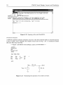
The CMOS circuit design process consists of defining circuit inputs and outputs, hand
calculations, circuit simulations, circuit layout, simulations including parasitics,
reevaluation of circuit inputs and outputs, fabrication, and testing. A flowchart of this
process is shown in Fig. 1.1. The circuit specifications are rarely set in concrete; that is,
they can change as the project matures. This can be the result of trade-offs made between
cost and performance, changes in the marketability of the chip, or simply changes in the
customer's needs. In almost all cases, major changes after the chip has gone into
production are not possible.
This text concentrates on custom IC design. Other (noncustom) methods of
designing chips, including field-programmable-gate-arrays (FPGAs) and standard cell
libraries, are used when low volume and quick design turnaround are important. Most
chips that are mass produced, including microprocessors and memory, are examples of
chips that are custom designed.
The task of laying out the IC is often given to a layout designer. However, it is
extremely important that the engineer can lay out a chip (and can provide direction to the
layout designer on how to layout a chip) and understand the parasitics involved in the
layout. Parasitics are the stray capacitances, inductances, pn junctions, and bipolar
2
CMOS Circuit Design, Layout, and Simulation
transistors, with the associated problems (breakdown, stored charge, latch-up, etc.). A
fundamental understanding of these problems is important in precision/high-speed
design.
Define circuit inputs
and outputs
(Circuit specifications)
^
I
T~
Hand calculations
and schematics
~~
I
1 "
,
Circuit simulations
^^^^
^^"^^
No
^
Does the circuit ^ >
^ ^ ^ ^ meet s p e c s ? ^
<
1
JYes
—->)
Layout
T
|
^
Re-simulate with parasitics
No ^ ^ ^ ^ D o e s the c i r c u u " ^ ^
^"^^^^^meet s p e c s ? ^ ^ ^ ^
JYes
>
Prototype fabrication
^
Test and evaluate
No, fab probleiTi/-^Q o e s t ^ e c i r c u i t ^ ^ ^ 0 ' s P ec Pr°blem
^ " " ^ \ ^ m e e t specs?^^^"^
Yes
\^
Production
|
Figure 1.1 Flowchart for the CMOS IC design process.
3
Chapter 1 Introduction to CMOS Design
1.1.1 Fabrication
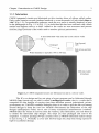
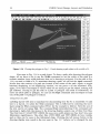
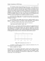
CMOS integrated circuits are fabricated on thin circular slices of silicon called wafers.
Each wafer contains several (perhaps hundreds or even thousands) of individual chips or
"die" (Fig. 1.2). For production purposes, each die on a wafer is usually identical, as seen
in the photograph in Fig. 1.2. In Fig. 1.2, an individual die has been outlined with a black
marker and appears next to a dime. Added to the wafer are test structures and process
monitor plugs (sections of the wafer used to monitor process parameters).
A dice fabricated with other die on the silicon wafer
•
\ . Enlarged
Wafer diameter is typically 100 to 300 mm.
Top (layout)
view
Side (cross-section)
view
200 mm wafer
(8 inches)
Figure 1.2 CMOS integrated circuits are fabricated on and in a silicon wafer.
The ICs we design and lay out using a layout program can be fabricated through
MOSIS (http://mosis.org) on what is called a multiproject wafer; that is, a wafer that is
comprised of chip designs of varying sizes from different sources (educational, private,
government, etc.). MOSIS combines multiple chips on a wafer to split the fab cost among
several designs to keep the cost low. MOSIS subcontracts the fabrication of the chip
designs (multiproject wafer) out to one of many commercial manufacturers (vendors).
MOSIS takes the wafers it receives from the vendors, after fabrication, and cuts them up
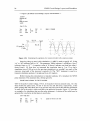
to isolate the individual chip designs. The chips are then packaged and sent to the
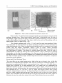
originator. A sample package (40-pin ceramic) from a MOSIS-submitted student design
is seen in Fig. 1.3. Normally a cover (not shown) keeps the chip from being exposed to
light or accidental damage.
4
CMOS Circuit Design, Layout, and Simulation
(a)
Chip
(b)
Bondwire
/
Bonding pad
Epoxytohold
chip in place
Figure 1.3 How a chip is packaged (a) and (b) a closer view.
Note, in Fig. 1.3, that the chip's electrical signals are transmitted to the pins of the
package through wires. These wires (called "bond wires") electrically bond the chip to
the package so that a pin of the chip is electrically connected (shorted) to a piece of metal
on the chip (called a bonding pad). The chip is held in the cavity of the package with an
epoxy resin ("glue") as seen in Fig. 1.3b.
The ceramic package used in Fig. 1.3 isn't used for most mass-produced chips.
Most chips that are mass produced use plastic packages. Exceptions to this statement are
chips that dissipate a lot of heat or chips that are placed directly on a printed circuit board
(where they are simply "packaged" using a glob of resin). Plastic packaged
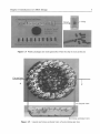
(encapsulated) chips place the die on a lead frame (Fig. 1.4) and then encapsulate the die
and lead frame in plastic. The plastic is melted around the chip. After the chip is
encapsulated, its leads are bent to the correct position. This is followed by printing
information on the chip (the manufacturer, the chip type, and the lot number) and finally
placing the chip in a tube or reel for shipping to a company that makes products that use
the chips. Example products might include chips that are used in cell phones, computers,
microwave ovens, printers.
Layout and Cross Sectional Views
The view that we see when laying out a chip is the top, or layout, view of the die.
However, to understand the parasitics and how the circuits are connected together, it's
important to understand the chip's cross-sectional view. Since we will often show a
layout view followed by a cross-sectional view, let's make sure we understand the
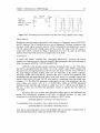
difference and how to draw a cross-section from a layout. Figure 1.5a shows the layout
(top) view of a pie. In (b) we show the cross-section of the pie (without the pie tin) at the
line indicated in (a). To "lay-out" a pie we might have layers called: crust, filling,
caramel, whipped-cream, nuts, etc. We draw these layers to indicate how to assemble the
pie (e.g., where to place nuts on the top). Note that the order we draw the layers doesn 't
matter. We could draw the nuts (on the top of the pie) first and then the crust. When we
fabricate the pie, the order does matter (the crust is baked before the nuts are added).
5
Chapter 1 Introduction to CMOS Design
Chip
Detail
Figure 1.4 Plastic packages are used (generally) when the chip is mass produced.
Cut pie here
(a) Layout view
(b) Cross-sectional view
Figure 1.5 Layout and cross sectional view of a pie (minus pie tin).
6
CMOS Circuit Design, Layout, and Simulation
1.2 Using the LASI Program
The LASI program discussed in this section can be used for the layout and design of
CMOS integrated circuits. This section provides a brief tutorial covering the use of LASI.
We assume that the reader has downloaded and installed LASI and the MOSIS setups
following the instructions at cmosedu.com. We use the MOSIS setups (with a design
directory of, for example, C:\Lasi7\Mosis) for our examples in this section.
1.2.1 The Basics of LASI
A chip design should reside in a design directory. The LASI system executables are
located in C:\Lasi7 (which cannot be used as a design directory). Information on setting
up a design directory can be found at cmosedu.com.
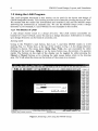
Starting LASI
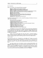
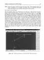
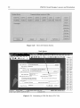
Going to the Window's start button, then Lasi 7, and then MOSIS results in LASI
starting, Fig. 1.6. Notice how, at the top of the window in Fig. 1.6, the design directory
(Folder) is shown. The menu items (Help, Run, Print, etc.) are executable by either
clicking on the word (e.g., Help) or on the menu button (e.g., the picture of a question
mark). The buttons on the right of the display can be toggled by either pressing the
Menul or Menu2 buttons or by clicking the right mouse button while in the drawing
area. We'll talk about the items on the bottom of the screen in a moment.
Figure 1.6 Starting LASI using the MOSIS setups.
Chapter 1 Introduction to CMOS Design
Getting Help
The LASI layout system comes with a complete on-line manual. This manual is
accessible, while LASI is running, by pressing Fl on the keyboard and clicking the
command button (simultaneously) with which the user needs help or by pressing the
Help button. Alternatively, the user can open the help file in the directory C:\Lasi7\help
without LASI running.
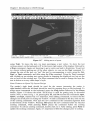
Cells in LASI I
Complex IC designs are made from simpler objects called cells. A cell might be a logic
gate or an op-amp. When LASI starts-up, as seen in Fig. 1.6, the last cell loaded (prior to
exiting LASI) appears in the load cell window. In Fig. 1.6, this cell's name is
"ALLMOSIS." Let's create a new cell called "test" with a rank of 1. Figure 1.7 shows the
resulting LASI screen. Notice that the current cell's name and rank are displayed at the
top of the window. If we want to load or create a different cell, we press either the Load
menu item or the corresponding picture, as indicated in Fig. 1.7. The drawing area in Fig.
1.7 shows a reference indicator (the origin of the drawing). To toggle displaying this
indicator, we can either press r on the keyboard or the R button in the lower right corner
of the display followed by redrawing the cell. To redraw the cell, we press Enter on the
keyboard or Draw or the picture of the pencil at the top of the window.
Cell name and rank
Load or create a cell
(clicking on the word or
picture results in the same action)
Figure 1.7 Screen after making a cell called "test" with a rank of 1.
8
CMOS Circuit Design, Layout, and Simulation
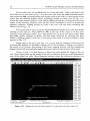
Navigating
Pressing the Grid button on the right of the screen followed by zooming in around the
reference indictor by pressing Zoom (and two clicks of the mouse to indicate the zoom
area) on the top menu may result in a screen like the one seen in Fig. 1.8. The reader
should experiment with the Fit (alt+f), Xpnd (alt+x or expand), and the arrow (Left, Up,
Dn, and Right) commands. The center command, Cntr, centers the screen around a point
set by the mouse. Pressing Last on the top menu brings up the previous (or last) view.
Figure 1.8 Navigating in LASI (see text).
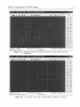
Drawing a Box
Let's draw a box. To start, select the Layr command and select "NWEL" or layer 42.
This is the n-well layer discussed in the next chapter. Remember that if a command isn't
showing, toggle the menus by right clicking the mouse in the drawing area or pressing
the buttons Menu 1 or Menu 2. Next select the Obj (object) command followed by
selecting BOX (double click on the word BOX). The lower left of the display should
indicate a working grid (Wgrd) of 1, a dot grid (Dgrd) of 1, a box object, and the n-well
layer. Next click on the Add button (we want to add a box on the n-well layer). The
lower left of the display should indicate that LASI is in the "Add Box" mode. By clicking
the left mouse once in the drawing area, moving the mouse, and clicking the left mouse
button again, we draw a box on the n-well layer. Figure 1.9 shows a possible resulting
display.
Chapter 1 Introduction to CMOS Design
9
Figure 1.9 Drawing a box using LASI.
Moving and Resizing
Moving or resizing an object consists of getting the object using, among others, the Get
command, moving the object using the Mov command, and putting (or deselecting) the
object using the Put command. For example, say we want to move the right edge of the
n-well box in Fig. 1.9. To begin, select the Get command. This is followed by clicking
the left button of the mouse on one side of the edge followed by clicking (the mouse) on
the other side of the edge (the selected or "Got" edge then becomes highlighted). Using
the Mov command, we can then use the mouse in the same manner to move the edge. To
deselect the edge, we use the Put command (again, in the same manner with the two
clicks of the left mouse button) or we simply press the all put (Aput) command. Note that
movement is relative to the clicking of the mouse (we don't have to click on the selected
edge). If, for example, the mouse is left-clicked somewhere in the drawing window and
then, in a horizontal distance of 5, left-clicked again, the selected edge will move
horizontally a distance of 5. (The user should experiment with these commands until they
feel comfortable.) To move the entire box, we get all four sides of the box or any part of
the box using the Fget (full get) command.
To reduce the amount of mouse clicking it is helpful to use the Qmov (quick
move) command. This command automatically performs the get, move, and put
commands in sequence so the user doesn't have to keep clicking menu items. The reader
should try out the Qmov command in LASI. Qmov can save considerable time when
making edits to layouts.
10
CMOS Circuit Design, Layout, and Simulation
The Drawing Grids
The position of the cursor in the drawing window is continuously read out at the bottom
of the screen. The value of the working grid (what the cursor snaps to) and the dot grid
(the dots we see when the Grid button is depressed) are also seen at the bottom of the
window. The coordinates of the cursor are either in working gridunits or in the smallest
possible grid unit, the unit grid (so that the cursor appears to move smoothly instead of
jumping around). For the MOSIS setups, there are 100 grid units between each working
grid point when the working grid is 1. By pressing the Wgrd and Dgrd buttons, the
respective working or dot grids are changed between one of ten possible values. These
values are set using the Cnfg command. (Again, if a command isn't showing, toggle the
menus by right clicking in the drawing window.) Figure 1.10 shows the Cnfg (configure
drawing parameters) window. In the MOSIS setups, we've limited the grids to either 1 or
0.5. Until the user gets familiar with layout, it's not a good idea to change these values.
Note that it's possible to have a dot grid of 1 while the working grid (the grid the cursor
snaps to) is 0.5.
Figure 1.10
Showing how the working and dot grids are set in LASI using the
Cnfg command.
Keyboard button a is a toggle between the working and unit grids. Pressing
keyboard button w causes the cursor to snap to the working grid while pressing u causes
the cursor to snap to the unit grid (i.e., appear to move in a continuous movement).
Making Measurements
LASI makes measurements using the keyboard buttons, z and spacebar. Pressing the z
button sets a zero reference point. Pressing the spacebar displays the distance between
the cursor and the zero reference point in the middle bottom of the window. It's useful to
remember at this point is that pressing w forces the cursor to snap to the working grid so
that measurements can be made based on the grid and independent of the state (the
current selected command) of LASI. Note that if the spacebar is held down, a continuous
measurement is displayed on the bottom of the window.
Chapter 1 Introduction to CMOS Design
11
Key Assignments
Below is a summary of the keyboard (button) commands.
Enter does a Draw command (redraws the display)
Delete does a Del command (deletes the selected objects)
Insert does a Xpnd command (expands the current view)
Home does a Cntr 0 0 command (centers the display on the origin [reference marker])
End does a Last command (switches back to the previous displayed view)
pgup pans up by a full screen
pgdn pans down by a full screen
arrows pan the drawing window in the direction of the pressed arrow
Tab toggles the mouse cursor between a small cross and crosshairs
z sets a measurement zero point
spacebar gives a measurement from the zero point
The following keyboard buttons are also executed by pressing on the button in the lower
right portion of the display
w forces the cursor to the working grid
u forces the cursor to the unit grid
c toggles the path center line on and off in a path object
d toggles the distance marker on and off
i toggles the cell image on and off (a dotted line around the silhouette of the cell)
n toggles the outline name on and off
o toggles the octagonal cursor mode on and off
r toggles the 0,0 reference mark on and off
t toggles the text reference point on and off
v toggles viewing vertices of a path or polygon object
The alt button can be used with the indicated letter in the top menu commands for
execution directly from the keyboard. For example, using alt+u (pressing alt followed by
u or pressing both at the same time) results in executing an Undo command. Other
multipurpose buttons include the Ctrl, Esc, and Shift buttons (see the LASI help manual
for additional information).
Finally note that pressing Esc (the escape key) aborts a command including a
Draw command. Using this command can be useful when the layout gets complicated
and large. Pressing escape stops the redrawing and shows the cells as simple outlines.
Cells in LASI II
Let's take the test cell in Fig. 1.9 and add it to a cell called test2. To begin, we press the
Load command button and create a cell called test2. LASI will ask if we want to save the
current cell, test, (select yes). Next LASI will ask what rank we want to assign the test!
cell. Select a rank of 2. A new cell will be created and the drawing window will become
blank.
The rank is used in the cell collection's (seen by pressing List) hierarchy. We
might rank a MOSFET cell with 1, an inverter cell with 2, and a counter cell with 5. The
MOSFET cell can be placed in the inverter or the counter but the inverter or counter
can't be placed in the MOSFET. Similarly, we can place the inverter (2) in the counter
(5) but we can't place the counter in the inverter. Note that to organize the cell collection
we go to the system menu (by pressing System) and then press Organize.
12
CMOS Circuit Design, Layout, and Simulation
We can add a box, as we did before, or we can add rank 1 cells to the rank 2 cell.
Let's add our test cell seen in Fig. 1.9 to this test2 cell. Press the Add command button.
Next select the Obj command button and double click on the cell test. Moving the mouse
cursor into the drawing display shows something similar to what's seen in Fig. 1.11.
Notice the small outline of the test cell. Before adding the cell (by clicking the left mouse
button in the drawing window), let's use the zoom command to zoom in around the
reference indicator. Adding several test cells to the test2 cell may look something like
what is seen in Fig. 1.12.
We can go back to the test cell by pressing List (saving the test2 cell) and double
clicking on the cell test. Press alt+f (or Fit) at the top of the menu to fit the cell's
contents to the drawing window. Let's add another box on the n-well layer (select Add,
then Obj, double clicking on BOX, and then Layr followed by selecting the layer
NWEL). Adding another n-well box to our layout may result in a layout similar to what
appears in Fig. 1.13.
Going back to the test2 cell, Fig. 1.14, we see that the changes in the layout are
automatically updated in the higher ranking cell. If, for example, a change was made to
the layout of an inverter, then going to the lower ranking inverter cell and making the
change (once) will automatically update the layout wherever the inverter cell is used.
Notice, in Fig. 1.14, that there is a dotted line surrounding the shape of the test
cell. These dotted lines are the image of the cell. In addition, there are small diamonds in
each of the added test cells. These diamonds indicate where the reference indicator is in
Figure 1.11 Adding the test cell with a rank of 1 to the test2 cell with a rank of 2.
Chapter 1 Introduction to CMOS Design
Figure 1.12 Adding several "test" cells with a rank of 1 to the "test2" cell with
a rank of 2.
Figure 1.13 Going back to the "test" cell and adding a additional n-well box.
13
14
CMOS Circuit Design, Layout, and Simulation
Figure 1.14 How the change to the "test" cell propagates up through the hierarchy.
the test cell. Moving or redefining the location of the reference indicator in the lower
ranking cell, using the Orig command, also shifts the cells' locations in the
higher-ranking cells where it is used. Pressing i on the keyboard or the I button at the
bottom of the display toggles the cell's image on and off. (To see the change, the drawing
window must be redrawn by pressing on the keyboard or using the Draw command.)
Moving a Cell
To move a cell, the Cget (cell get) command is used first. Double clicking on the cell or
using the mouse to surround a cell (or cells) "gets" the cell. This is followed by using the
Mov command. Deselecting the cells can be accomplished using the Cput (cell put)
command or, more often, using the Aput (all put) command.
Viewing or Editing Specific Layers
When layouts get complicated, the ability to look at or edit specific layers becomes
important. However, someone learning layout can also feel frustrated by not knowing
how the viewing and editing of specific layer commands operate. Below we summarize
these commands.
Ldrw Draws only one layer of the layout. Useful to quickly view a single layer.
View Selects the layers LASI displays in the drawing window. This command can be
frustrating. For example, suppose the NWEL layer is deselected in the view
menu. If we were to draw a box on the NWEL layer and then redraw the layout,
the box we just drew wouldn't show up!
Chapter 1 Introduction to CMOS Design
15
Open Selects the layers LASI will allow the user to "get." This command, again, can
result in frustration. If, for example, the NWEL layer is not selected in the open
menu, then trying to "get" the layer will result in a waste of time.
The Polygon and Path Shapes
The only drawing shape we've discussed so far is the box. LASI can also be used to
make polygons and path shapes. Let's start out by drawing a polygon (say a triangle).
Create a new cell (using the Load command) called test3 with a rank of 1. Select Add,
then Obj (double clicking on PATH/POLY). Let's also select a different layer using the
Layr command (select POL1 or layer 46). Next click the Wdth command and make sure
that width is set to 0. When the width is zero, the object is a polygon. When the width is
nonzero, the object is a path. Figure 1.15 shows the layout of a polygon (not closed).
Notice the location of the polygon's vertices. To move (or change) the shape of a
polygon, we must get a vertex. Using the Get command on a side of a polygon, and not
encompassing a vertex, can result in frustration. To show the polygon's (or path's)
vertices in the drawing display, press v on the keyboard (or the V in the lower right
corner of the display) followed by Enter. (Try this now.) To close the polygon object in
Fig. 1.15, we place the last (fourth) vertex on the first vertex as seen in Fig. 1.16. Note
that this last vertex is still active and so it appears that we are still drawing the same
polygon (even though our triangle is closed). To draw another shape, click the Aput
command.
Figure 1.15 Drawing a polygon in LASI on the POL1 (polysilicon) layer.
CMOS Circuit Design, Layout, and Simulation
16
Figure 1.16 Closing the polygon in Fig. 1.15 and drawing a path object with a width of 4.
Also seen in Fig. 1.16 is a path object. To draw a path, after drawing the polygon
shape, all we have to do is use the Wdth command to set the width of the path to a
nonzero number (zero width indicates that we're drawing a polygon). For the path in Fig.
1.16, we used a width of 4. To terminate drawing a path, we can use the Aput command.
Notice how the vertices of a path are located in the center of the path. Again, to toggle
between displaying or not displaying vertices, we can press v on the keyboard. Also,
again, if we don't encompass a vertex when we are trying to get the object, nothing will
get selected. (Trying to get the side of a path or polygon can result in frustration.) To
move an entire path or polygon, we can use the Fget command and encompass at least
one of the path's or polygon's vertices.
Using Text in LASI
Labeling layout with text is important for documenting how the IC is assembled. To add
text to a layout, we select the Text command. This is followed by selecting the text's
layer using the Tlyr command (select POL1 for the example to follow). Next the size of
the text can be set using Tsiz. The command Font (remembering if the command isn't
showing to right-click the mouse in the drawing display) selects one of three font files.
The first font (C:\LASI7\TFF1.DBD) file uses zero-width letters (so they don't have any
fabrication significance). The other files (TFF2.DBD and TFF3.DBD) do have widths,
and so they can be seen in the fabricated chips. Clicking the left mouse button in the
drawing display may result in the text seen in Fig. 1.17 (where we've changed the size
Chapter 1 Introduction to CMOS Design
17
Figure 1.17 Adding text to a layout.
using Tsiz). To move the text, we must encompass a text vertex. To show the text
vertices, press t on the keyboard or T in the lower right corner of the display followed by
a Draw command. Again, not knowing to get a vertex can lead to frustration. To get text
in a layout without getting any of the other objects, we can use the Tget command. To
change the size of the text, we "get" the text by encompassing a vertex using the Get,
Fget, or Tget commands, and then using the Csiz command. Using the Text command
and clicking on an existing text vertex results in changing the displayed text but not the
size or layer of the existing text. The Clyr command can be used to change the layer the
text is drawn on or any other shape's layer.
Some Features to Speed Up Layout Design
The reader's right hand should be used for the mouse (assuming the reader is
right-handed) while the left hand should be used for pressing keys on the keyboard. To
assign more commands to the keyboard, press the Cnfg button followed by the Fkeys
button. Figure 1.18 shows the result. The Fl key is used for getting help, as discussed
earlier. Now, as seen in Fig. 1.18, pressing F2, F3, and F4 executes the commands Aput,
Qmov, and Fget, respectively. It's important, when adding commands, to ensure that the
changes are saved prior to exiting the window. To add a command to the list, click on one
of the existing commands. Next type the new command in the command argument field
at the bottom of the window. Pressing Add places the new command after the selected
existing command, while pressing Insert places the command before the existing
command. To edit an existing command, double click on it. After editing, press Paste to
update the existing command. Again, it's important to Save the changes prior to exiting.
18
CMOS Circuit Design, Layout, and Simulation
Figure 1.18 Setting up the Fkeys to speed up layout.
Some other useful commands that can speed up layout, when the layout contains a
large number of cells, are the Outl, Full, and Dpth commands. To avoid having to
redraw the contents of a cell or cells, the Outl (outline) command can be used. Either
double-clicking on a cell or surrounding the cell's contents with the mouse, when the
Outl command is selected, causes the cells to be drawn as outlines. Pressing n on the
keyboard or N with the mouse cursor in the lower right portion of the display, toggles the
cell's name in its outline on and off. Using the Full command shows the contents of the
cell.
If we are editing a cell with lower ranking cells nested in it, then we can use the
Dpth (depth) command to limit the full display of these lower ranking cells. If depth is
set to 0, then only the basic objects (boxes, paths, text) in the current-edited cell are
shown in detail. The lower level cells are shown as dashed outlines. If the depth is set to
1, then the basic objects in the next level of nested cells are shown ... and so on. Note that
cell nesting levels are not the same as cell rank. To show the basic objects of all possible
nested cells, the depth should set to 15. To see a listing of nested cells within other cells,
use the Show command.
Finally, when editing both cells and objects (boxes, polygons, and paths) the
window get, Wget (window get) and, Wmov (window move) commands can be very
useful. While in the Wget command mode, the mouse is used to select an area of layout
containing both cells and drawn objects. The Wmov command moves this layout. Note
that when "getting" the layout a cell won't be selected unless it is completely surrounded
in the mouse selection area.
Understanding the Cpy and Copy Commands
The Cpy command is used to copy layout within a cell. The layout is selected using, for
example, the Fget, Cget, or Wget commands. The Cpy command then behaves just like
a move command except that the selected layout isn't moved to the new location: it is
copied.
Chapter 1 Introduction to CMOS Design
19
It's important to understand that using the Cpy command frequently is not a good
idea. For example, say a memory cell containing 50 objects (boxes, polygons, or paths) is
laid out. If the memory cell is used in a 1 Mbit memoiy, and the Cpy command is used,
then the resulting number of objects in the memory cell is 50 million (this is bad). If, on
the other hand, the 1 Mbit memory is made with the 1,000,000 memory cells, then the
size (the number of objects) is 1,000,050. We can take this a step further. We can make a
cell containing a row of memory cells (say 1,000) and use this row cell 1,000 times to
make a 1 Mbit memory. The number of objects in the 1 Mbit memory cell is now only
2,050 (1,000 instances of the memory row, 1,000 instances of the memory bit, and 50
objects in the memory bit). We can take this even further to reduce the size of the layout
file. Using cell hierarchy is extremely important. Do not lay out a large chip unless the
material in this paragraph is understood! Else the design file sent to the mask maker will
be unreasonably large. Use the Cpy command as little as possible.
Using the Save command saves the contents of the cell we are working on. It can
also be used to save the cell under a different name. However, sometimes we want to take
some portion of the layout we are working on and move it (append it) to a different cell
(or a new cell). The Copy command is useful for this task. To take some layout and
append it to a different cell, we first "get" the layout we want to copy to a different cell.
Next we select the Copy command and the cell we want to move the selected layout into
(or the name of a new cell).
Transporting Cells in LASI
To share files between other users or between design directories, Transportable LASI
Cell files (*.TLC) files or Transportable LASI Drawing files (*.TLD) files are used. The
files we draw in LASI are saved on the hardisk as text files with the TLC extension.
Copying TLC files into a directory will not make them show up in the design
directory's cell listing (and so we won't be able to edit the cells). To register a cell in a
design directoiy, we must first Import the cell. Note, in the System menu, the Organize
command can be used to organize the cells in a design directory according to rank or
name.
The TLC files contain references to other cells but not the actual layouts of the
referenced cells themselves. (For example, a reference may indicate "place the inverter
cell at the location 12,13.") To get a file that contains the cell's hierarchy, we use TLD
files. To generate a TLD file, we go to the Export command and select the name of the
cell, TLD file, and the location we want to place the TLD file. TLD files can be shared
between users or used as backups of work. Note that while LASI imports a TLD file, it
still uses TLC files for editing. Every time Save is pressed, the TLC file in the design
directory (being edited) is updated, leaving the TLD file unchanged (until the Export
command is used).
Edit-in-Place
Consider the layout seen in Fig. 1.19. In this layout we have two boxes and two cells.
Let's say we want to align the cell on the right to the two boxes. The simplest way to do
this (keeping in mind that modifying the cell propagates through the hierarchy) is to get
the cell using the Cget command. Then press Ctrl on the keyboard while pressing Load.
This causes LASI to enter the "Edit-in-Place" (EIP) mode. A lower ranking cell can then
be modified while showing the objects from the higher ranking cell. To exit EIP, use the
CMOS Circuit Design, Layout, and Simulation
20
Figure 1.19 Editing a cell in place.
Load or List commands. Note that the other cells in the layout will not be shown when in
EIP mode (only the cell we are editing and the drawn objects from the higher ranking
cell).
Backing Up Your Work
It's very important to constantly back up your work in a location other than the hard disk
you are running LASI out of. Backups can be as simple as exporting TLD files to a DVD
or as complete as copying the design directory (or zipping it up) to a network drive. The
point is layout that is laborious so not backing up the work is a mistake.
1.2.2 Common Problems
After adding an object, the object cannot be seen
Check the View layers in the drawing display to ensure that the layer is not in hidden
mode. The Draw command must be used after using View.
Cannot Get an object
(1) Check, using the Open command, that the layer can be opened (or moved). (2) Verify
that the object is not part of another cell. (3) When trying to get an object made using the
path or polygon object make sure that the cursor encompasses a vertex. (4) If the object is
text, then text vertex must be encompassed.
Chapter 1 Introduction to CMOS Design
21
Cells are drawn as outlines, or the perimeter of a cell has a dashed line
(1) Use the Full command to show the contents of a cell. (2) Use the Dpth command to
limit the depth of the cells shown. Increasing the depth to the rank of the cell shows all
cells. (3) Press i on the keyboard to force an outline to be drawn around a ceil. This is
indicated by the I in the bottom right corner of the drawing display. The letter n (or N in
the lower right of the display) toggles the display of the cell's name.
Fit command causes the drawing window to expand much larger than the current cell
There is an unknown object someplace in the cell. Use the Fget command to get any
objects outside the main cell area. Use the Del command to delete the unknown object.
Cursor movement is not smooth
(1) The cursor may be in the octagonal mode. Press o on the keyboard or the button O in
the lower right portion of the display to toggle this mode on and off. (2) Make sure that
the display isn't zoomed in too much. (3) Pressing a can be used to toggle the mouse
cursor between the working and unit grids.
1.2.3 Sending the Layout to the Mask Maker
Once we have a completed layout we can convert the resulting TLC files into a format
the mask maker will accept. These formats are either CIF (CalTech intermediate format)
or GDS (graphical design system, which is a derivative of the older Calma stream format,
CSF). We'll focus on using GDS (at the time of this writing the format is actually a
second-generation standard called GDSII) since it is what is used in industry. Generating
a *.GDS file in LASI (or any other layout program) is often called streaming the layout
out. Because GDS files can be large, and they are often stored on magnetic storage tapes,
generating and storing the GDS file is often called "taping out" or simply "tape-out."
Assuming the layout is saved, we enter the System mode in LASI, Fig. 1.20.
Next, we select the Tlc2Gds command button, Fig. 1.21. The specific details concerning
using this utility or the Gds2Tlc utility can be found in the on-line manual. One of the
important parameters in the setups is the scale factor Lambda. This takes our layout
drawn on a " 1" grid and scales it to the appropriate final size.
Checking to Make Sure the Layout Scaled Correctly
To ensure that the layout scales correctly when making the GDS file, copy the design
directory into a temporary design directory (TDD). LASI is then set up to run from this
TDD. This ensures that all of the original layout isn't corrupted by mistakes in the
checking process we're about to discuss (important). It's also a good idea to back up the
directory at this point as well.
In this TDD we can generate a GDS file, using the Tlc2Gds utility. Unless, the
user has some atypical needs (e.g., eliminating layers in the final GDS file), this is a
simple matter of specifying the name of the TLC file to convert (ensuring the TLC file in
the dummy directory is used), specifying the name of the GDS file to create from the
TLC file, specifying the scale factor, and starting the conversion (pressing Go) after
exiting the setups. Both GDS and layer data map (*.ldm) files are generated. (The user
will have to select the layers to add to the ldm file while the conversion is in progress
unless an ldm file already exists.) The *.ldm file is used when converting the GDS back
into a TLC file discussed below.
22
CMOS Circuit Design, Layout, and Simulation
Figure 1.20 The LASI System Screen.
Scale factor
Figure 1.21 Generating a GDS file from a TLC file.
Chapter 1 Introduction to CMOS Design
23
After the GDS file is generated, we can use the Gds2Tlc program to convert the
GDS file back into TLC files. In the setups we must specify a directory where the TLC
files will be written, for example, C:\temp. We can't use a drawing directory because
then the existing TLC files would be overwritten. After we've converted the GDS back
into TLC files, we can Import the (scaled) TLC files into the dummy directory to make
sure the generated GDS file is scaled correctly.
Note, for the sake of feeling comfortable with this process, that it's easy to take a
simple cell, like the test cell in Fig. 1.9 and convert it back and forth between a GDS file
and a TLC file (with scale factor). Also note that we can use the Resize command on the
system menu to change the size of the layout if needed.
1.3 An Introduction to WinSPICE
The simulation program with an integrated circuit emphasis (SPICE) is a ubiquitous
software tool for the simulation of circuits. In this book we'll use WinSPICE. See the
links at cmosedu.com for download and installation information. WinSPICE, like all
SPICE engines, uses a text file netlist for simulation input.
Generating a Netlist File
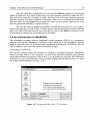
We can use, among others, the Window's notepad or wordpad programs. WinSPICE
likes to see files with a "*.cir" extension. To save a file with this extension, place the file
name and extension in quotes as seen in Fig. 1.22. If quotes are not used, then Windows
will tack on ".txt" to the filename. This can make finding the file difficult when we open
the netlist with WinSPICE (see Fig. 1.23).
Putting the file name with
extension (cir) in quotes
won't tack on the gratuitous
.txt to the end of the filename.
Figure 1.22 Saving a text file with a ".cir" extension.
24
CMOS Circuit Design, Layout, and Simulation
B Copyright 1996-2003 OuseTech Ltd. n i l Rights Reserved.
1.85.81
Dec 18 2003
Opening
a circuit Shareware uersion of
netlist. Please read the file
80:47:53
MinSpice. For non-comnercial use only.
'license.txt' for conditions of use.
Type "help" for more information, "quit" to leaue.
UinSpice 1 -> _
Figure 1.23 Opening a file with WinSPICE.
Transient Analysis
A SPICE transient analysis simulates circuits in the time domain (like an oscilloscope the
x-axis is time). Let's simulate the simple circuit seen in Fig. 1.24. A simulation netlist
(the text file) may look like:
*** Figure 1.25 CMOS: Circuit Design, Layout, and Simulation ***
.control
destroy all
run
plot vin vout
.endc
.tran 100p 100n
Vin
R1
R2
Vin
Vin
Vout
0
Vout
0
DC
1k
2k
1
.end
Vin
Rl>
lk
A AA
Vin, 1 V
Figure 1.24
Vout
R2,2k
Simulating the operation of a resistive divider.
25
Chapter 1 Introduction to CMOS Design
The simulation results using this netlist are seen in Fig. 1.25. The first line in a
netlist is a title line. This line is ignored by SPICE (important). The next five lines are
control commands. Notice how the end of the control statement is terminated with an
".endc" not an ".end" like at the end of the netlist. Placing ".end" at the end of the control
statement causes SPICE to ignore all of the lines containing the circuit information. The
statements in the control block can be run directly from the command line in the
WinSPICE command window seen in Fig. 1.23. The destroy all command destroys all of
the previous simulation results (so we don't display old data). The run command runs the
simulation. The plot command plots the voltages on the nodes Vin and Vout.
Note that the DC voltage source Vin is connected to the node Vin. We could have
labeled the Vin node with a number like " 1 . " However, it is nice to have node names that
correspond with signals.
The connection of the resistors and how they are specified should be easy to
determine. A line starting with an "R" indicates a resistor specification. A line beginning
with an "*" indicates a comment. Node 0 (zero) is always reserved for ground.
The form of the transient statement (this is the type of analysis) is
TRAN TSTEP TSTOP <TSTART> <TMAX> <UIC>
where the terms in < > are optional. The TSTEP term indicates the (suggested) time step
to be used in the simulation. The parameter TSTOP indicates the simulation's stop time.
The starting time of a simulation is always time equals zero. However, for very large
(data) simulations, we can specify a time to start saving data, TSTART (again this term is
optional). The TMAX parameter is used to specify the maximum step size. If the plots start
to look jagged (like a sinewave that isn't smooth), then TMAX should be reduced.
1.00,
1
;
•
;
0 90
1
\
\
•
0 BO —
-
i
o.70
\
\
:
i
'-
:
j
i
j
j
:
0.60
0.0
^VOUt
20.0
'
40.0
time
L
60.0
nS
\
!
:
80.0
\
— i
ivin
J
100.0
Figure 1.25 Simulating the circuit in Fig. 1.24.
To illustrate a simulation using a sinewave, examine the schematic in Fig. 1.26.
The statement for a sinewave in SPICE is
SIN VO VA FREQ <TD> <THETA>
The parameter VO is the sinusoid's offset (the DC voltage in series with the sinewave).
The parameter VA is the peak amplitude of the sinewave. FREQ is the frequency of the
sinewave, while TD is the delay before the sinewave starts in the simulation. Finally,
THETA is used if the amplitude of the sinusoid has a damped nature. To simulate the
circuit in Fig. 1.26, we use a netlist of
CMOS Circuit Design, Layout, and Simulation
26
*** Figure 1.26 CMOS: Circuit Design, Layout, and Simulation ***
.control
destroy all
run
plot vin vout
.endc
.tran 1n 3u
Vin
R1
R2
Vin
Vin
Vout
0
Vout
0
DC
1k
2k
0
SIN 0 1 1MEG
.end
Vout
1 0
Vin
IV (peak) at
1MHz
0 5
0.0
-0 5
-1 0
0 0
0
0.5
10
time
1.5
2 0
uS
2 5
3 0
Figure 1.26 Simulating the operation of a resistive divider with a sinewave input.
Some key things to note in this simulation: (1) MEG is used to specify 106. Using
"m" or "M" indicates milli or 10~3. The parameter 1MHz indicates 1 milliHertz. (Also, f
indicates femto or 10~15. A capacitor value of If doesn't indicate one farad but rather 1
femto Farad.) (2) Note how we increased the simulation time to 3 |is. If we had a
simulation time of 100 ns (as in the previous simulation), we wouldn't see much of the
sinewave (one-tenth of the sinewave's period). (3) The "SIN" statement is used in a
transient simulation analysis. It is not used in an AC analysis.
Before leaving this introduction to transient analysis, let's introduce the SPICE
pulse statement. This statement has a format given by
PULSE VINIT VFINAL TD TR TF PW PER
VINIT is the pulse's initial voltage, VFINAL is the pulse's final (or pulsed) value, TD is the
delay before the pulse starts, TR and TF are the rise and fall times, respectively, of the
pulse (noting that when these are set to zero the step size used in the transient simulation
is used); PW is the pulse's width; and PER is the period of the pulse. Figure 1.27 provides
an example of a simulation that uses the pulse statement. A section of the netlist used to
generate the waveforms in this figure is seen below.
.tran 100p30n
Vin
R1
C1
Vin
Vin
Vout
0
Vout
0
DC
1k
1p
0
pulse 0 1 6n 0 0 3n 10n
27
Chapter 1 Introduction to CMOS Design
Rl, Ik
Otol V
delay 6ns
time at 1 V = 3 ns
period = 10 ns
Vout
1.0
0 8
0 6
0.4
0.2
0.0
0.
0.O
5.0
10.0
time
15 0
20 0
nS
25 0
30 0
Figure 1.27 Simulating the step response of an RC circuit using a pulsed source voltage.
Other Analysis
Besides the transient analysis presented in this section, we frequently use the SPICE DC
and AC analyses. The AC analysis has an x-axis of frequency. This type of analysis is the
common "small-signal" analysis used in a basic introductory microelectronics course.
The DC analysis has a DC voltage source for the x-axis. The value of the DC source is
swept while either a current of voltage is plotted on the y-axis. We don't go into these
analyses here but provide numerous examples later in the book.
Convergence
A netlist that doesn't simulate isn't converging numerically. Assuming the circuit
contains no connection errors, there are basically three parameters that can be adjusted to
help convergence: ABSTOL, VNTOL, and RELTOL.
ABSTOL is the absolute current tolerance. Its default value is 1 pA. This means
that when a simulated circuit gets within 1 pA of its "actual" value, SPICE assumes that
the current has converged and moves onto the next time step or AC/DC value. VNTOL is
the node voltage tolerance, default value of 1 \xW. RELTOL is the relative tolerance
parameter, default value of 0.001 (0.1 percent). RELTOL is used to avoid problems with
simulating large and small electrical values in the same circuit. For example, suppose the
default value of RELTOL and VNTOL were used in a simulation where the actual node
voltage is 1 V. The RELTOL parameter would signify an end to the simulation when the
node voltage was within 1 mV of 1 V (1V-RELTOL), while the VNTOL parameter
signifies an end when the node voltage is within 1 uV of 1 V. SPICE uses the larger of
the two, in this case the RELTOL parameter results, to signify that the node has
converged.
Increasing the value of these three parameters helps speed up the simulation and
assists with convergence problems at the price of reduced accuracy. To help with
convergence, the following statement can be added to a SPICE netlist:
.OPTIONS ABSTOL=1 uA VNTOL=1 mV RELTOL=0.01
To (hopefully) force convergence, these values can be increased to
.OPTIONS ABSTOL=1mAVNTOL=100mVRELTOL=0.1
Note that in some high-gain circuits with feedback (like the op-amp's designed later in
the book) decreasing these values can actually help convergence.
28
CMOS Circuit Design, Layout, and Simulation
Some Common Mistakes and Helpful Techniques
The following is a list helpful techniques for simulating circuits using SPICE.
1.
The first line in a SPICE netlist must be a comment line. SPICE ignores the first
line in a netlist file.
2.
One megaohm is specified using 1MEG, not 1M, lm, or 1 MEG.
3.
One farad is specified by 1, not If or IF. IF means one femto-farad or 10~15
farads.
4.
Voltage source names should always be specified with a first letter of V. Current
source names should always start with an I.
5.
Transient simulations display time data; that is, the x-axis is time. A jagged plot
such as a sinewave that looks like a triangle wave or is simply not smooth is the
result of not specifying a maximum print step size.
6.
Convergence with a transient simulation can usually be helped by adding a UIC
(use initial conditions) to the end of a .tran statement.
7.
A simulation using MOSFETs must include the scale factor in a .options
statement unless the widths and lengths are specified with the actual (final) sizes.
8.
In general, the body connection of a PMOS device is connected to VDD, and the
body connection of an n-channel MOSFET is connected to ground. This is easily
checked in the SPICE netlist.
9.
Convergence in a DC sweep can often be helped by avoiding the power supply
boundaries. For example, sweeping a circuit from 0 to 1 V may not converge, but
sweeping from 0.05 to 0.95 will.
10.
In any simulation adding .OPTIONS RSHUNT=1E8 (or some other value of
resistor) can be used to help convergence. This statement adds a resistor in
parallel with every node in the circuit (see the WinSPICE manual for information
concerning the GMIN parameter). Using a value too small affects the simulation
results.
ADDITIONAL READING
[1]
D. E. Boyce, LASI User's Manual, available while LASI is running by pressing
Fl on the keyboard and the button the user needs help with (at the same time).
Alternatively, the user can open the help file in the directory C:\Lasi7\help.
[2]
M. Smith, WinSPICE User's Manual, Available for download (with the
WinSPICE simulation program) at http://www.winspice.co.uk/
PROBLEMS
In the following solutions, it can be very helpful to use the Prt Sc (print screen) button on
the keyboard to copy contents displayed on the computer's display to the clip board. The
image of the display can then be pasted into a document. For ease of viewing (the
resulting pasted image in the document), it may also be useful reduce the display
resolution prior to using the Prt Sc button (right click on the desktop, select properties,
then settings).
Chapter 1 Introduction to CMOS Design
29
In the following problems, the solutions should include pictures of the LASI
layout screen and discussions indicating that you know what you are doing.
1.1
Create a cell called mycell with a rank of 1 using LASI. In this cell, draw a 10 by
10 box using the POL1 layer. Place the lower left corner of the box at the origin.
Show how to measure the diagonal distance of the box.
1.2
Explain how the Qmov command can be used to edit the box in Problem 1 so that
it measures 5 by 8. How would this be accomplished using Get, Mov, and Put?
1.3
What functions do the Swin and Rwin commands perform? Give an example of
where these would be useful.
1.4
What functions do the Cget and Cput commands perform? Can any other
commands be used in place of Cget?
1.5
Write the word "test" on the MET1 layer with sizes of 3, 9, and 24 in the cell of
Problem 1 (mycell). Discuss the possible ways of "getting" the text and "moving "
text.
1.6
Using a path and a polygon in the cell (mycell) of Problem 1, generate two objects
with widths of 10 and lengths of 10 directly next to the box from Problem 1.
Discuss the differences in editing boxes, polygons, and paths.
1.7
Explain, in your own words, the difference between the Cpy and Copy
commands. Give examples to demonstrate the differences.
1.8
Demonstrate how the Wget and Wmov commands function.
1.9
Using the POL1 layer, draw a triangle that measures nominally 10 on each side
(make sure the layout is snapped to the working grid). How many vertices does
the triangle have? Using LASI's measurement tools, measure the length of the
triangle's sides.
1.10
Circles can be drawn using a polygon (path with zero width) and the Arc
command. Show how to draw a circle using LASI. Make sure the steps are clear.
1.11
What does the Clone system command do? Give an example of how to use this
command.
1.12
Discuss the different ways cells can be drawn as outlines.
1.13
What do the keyboard buttons w, u, a, z, and space do in LASI? Give examples to
illustrate your understanding of each key's function.
1.14
Describe how to add text in LASI and how to set the text size and layer.
1.15
Explain, in your own words and with examples, how to edit a cell in place.
1.16
Simulate the operation of the circuit in Fig. 1.28. What happens if you use a pulse
frequency that's too high? What happens if your simulation time is too short?
Give examples to illustrate your understanding.
30
CMOS Circuit Design, Layout, and Simulation
Ik
An input pulse.
T
iP
£ ik
Figure 1.28 Circuit used in Problem 1.16