1
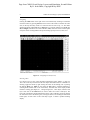
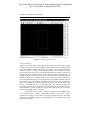
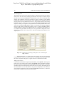
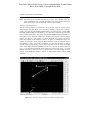
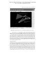
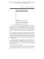
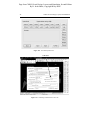
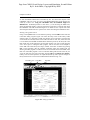
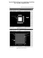
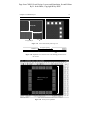
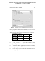
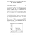
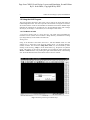
Page from CMOS Circuit Design, Layout, and Simulation, Second Edition By R. Jacob Baker, Copyright Wiley-IEEE 6 CMOS Circuit Design, Layout, and Simulation 1.2 Using the LASI Program The LASI program discussed in this section can be used for the layout and design of CMOS integrated circuits. This section provides a brief tutorial covering the use of LASI. We assume that the reader has downloaded and installed LASI and the MOSIS setups following the instructions at cmosedu.com. We use the MOSIS setups (with a design directory of, for example, C:\Lasi7\Mosis) for our examples in this section. 1.2.1 The Basics of LASI A chip design should reside in a design directory. The LASI system executables are located in C:\Lasi7 (which cannot be used as a design directory). Information on setting up a design directory can be found at cmosedu.com. Starting LASI Going to the Window’s start button, then Lasi 7, and then MOSIS results in LASI starting, Fig. 1.6. Notice how, at the top of the window in Fig. 1.6, the design directory (Folder) is shown. The menu items (Help, Run, Print, etc.) are executable by either clicking on the word (e.g., Help) or on the menu button (e.g., the picture of a question mark). The buttons on the right of the display can be toggled by either pressing the Menu1 or Menu2 buttons or by clicking the right mouse button while in the drawing area. We’ll talk about the items on the bottom of the screen in a moment. Figure 1.6 Starting LASI using the MOSIS setups. Page from CMOS Circuit Design, Layout, and Simulation, Second Edition By R. Jacob Baker, Copyright Wiley-IEEE Chapter 1 Introduction to CMOS Design 7 Getting Help The LASI layout system comes with a complete on-line manual. This manual is accessible, while LASI is running, by pressing F1 on the keyboard and clicking the command button (simultaneously) with which the user needs help or by pressing the Help button. Alternatively, the user can open the help file in the directory C:\Lasi7\help without LASI running. Cells in LASI I Complex IC designs are made from simpler objects called cells. A cell might be a logic gate or an op-amp. When LASI starts-up, as seen in Fig. 1.6, the last cell loaded (prior to exiting LASI) appears in the load cell window. In Fig. 1.6, this cell’s name is “ALLMOSIS.” Let’s create a new cell called “test” with a rank of 1. Figure 1.7 shows the resulting LASI screen. Notice that the current cell’s name and rank are displayed at the top of the window. If we want to load or create a different cell, we press either the Load menu item or the corresponding picture, as indicated in Fig. 1.7. The drawing area in Fig. 1.7 shows a reference indicator (the origin of the drawing). To toggle displaying this indicator, we can either press r on the keyboard or the R button in the lower right corner of the display followed by redrawing the cell. To redraw the cell, we press Enter on the keyboard or Draw or the picture of the pencil at the top of the window. Cell name and rank Load or create a cell (clicking on the word or picture results in the same action) The mouse can be toggled between a cross and and crosshairs by pressing the tab button. Reference marker (drawings origin) Location of the mouse Toggles display of the reference marker Figure 1.7 Screen after making a cell called "test" with a rank of 1. Page from CMOS Circuit Design, Layout, and Simulation, Second Edition By R. Jacob Baker, Copyright Wiley-IEEE 8 CMOS Circuit Design, Layout, and Simulation Navigating Pressing the Grid button on the right of the screen followed by zooming in around the reference indictor by pressing Zoom (and two clicks of the mouse to indicate the zoom area) on the top menu may result in a screen like the one seen in Fig. 1.8. The reader should experiment with the Fit (alt+f), Xpnd (alt+x or expand), and the arrow (Left, Up, Dn, and Right) commands. The center command, Cntr, centers the screen around a point set by the mouse. Pressing Last on the top menu brings up the previous (or last) view. Figure 1.8 Navigating in LASI (see text). Drawing a Box Let’s draw a box. To start, select the Layr command and select “NWEL” or layer 42. This is the n-well layer discussed in the next chapter. Remember that if a command isn’t showing, toggle the menus by right clicking the mouse in the drawing area or pressing the buttons Menu 1 or Menu 2. Next select the Obj (object) command followed by selecting BOX (double click on the word BOX). The lower left of the display should indicate a working grid (Wgrd) of 1, a dot grid (Dgrd) of 1, a box object, and the n-well layer. Next click on the Add button (we want to add a box on the n-well layer). The lower left of the display should indicate that LASI is in the “Add Box” mode. By clicking the left mouse once in the drawing area, moving the mouse, and clicking the left mouse button again, we draw a box on the n-well layer. Figure 1.9 shows a possible resulting display. Page from CMOS Circuit Design, Layout, and Simulation, Second Edition By R. Jacob Baker, Copyright Wiley-IEEE Chapter 1 Introduction to CMOS Design 9 Figure 1.9 Drawing a box using LASI. Moving and Resizing Moving or resizing an object consists of getting the object using, among others, the Get command, moving the object using the Mov command, and putting (or deselecting) the object using the Put command. For example, say we want to move the right edge of the n-well box in Fig. 1.9. To begin, select the Get command. This is followed by clicking the left button of the mouse on one side of the edge followed by clicking (the mouse) on the other side of the edge (the selected or “Got” edge then becomes highlighted). Using the Mov command, we can then use the mouse in the same manner to move the edge. To deselect the edge, we use the Put command (again, in the same manner with the two clicks of the left mouse button) or we simply press the all put (Aput) command. Note that movement is relative to the clicking of the mouse (we don’t have to click on the selected edge). If, for example, the mouse is left-clicked somewhere in the drawing window and then, in a horizontal distance of 5, left-clicked again, the selected edge will move horizontally a distance of 5. (The user should experiment with these commands until they feel comfortable.) To move the entire box, we get all four sides of the box or any part of the box using the Fget (full get) command. To reduce the amount of mouse clicking it is helpful to use the Qmov (quick move) command. This command automatically performs the get, move, and put commands in sequence so the user doesn’t have to keep clicking menu items. The reader should try out the Qmov command in LASI. Qmov can save considerable time when making edits to layouts. Page from CMOS Circuit Design, Layout, and Simulation, Second Edition By R. Jacob Baker, Copyright Wiley-IEEE 10 CMOS Circuit Design, Layout, and Simulation The Drawing Grids The position of the cursor in the drawing window is continuously read out at the bottom of the screen. The value of the working grid (what the cursor snaps to) and the dot grid (the dots we see when the Grid button is depressed) are also seen at the bottom of the window. The coordinates of the cursor are either in working grid units or in the smallest possible grid unit, the unit grid (so that the cursor appears to move smoothly instead of jumping around). For the MOSIS setups, there are 100 grid units between each working grid point when the working grid is 1. By pressing the Wgrd and Dgrd buttons, the respective working or dot grids are changed between one of ten possible values. These values are set using the Cnfg command. (Again, if a command isn’t showing, toggle the menus by right clicking in the drawing window.) Figure 1.10 shows the Cnfg (configure drawing parameters) window. In the MOSIS setups, we’ve limited the grids to either 1 or 0.5. Until the user gets familiar with layout, it’s not a good idea to change these values. Note that it’s possible to have a dot grid of 1 while the working grid (the grid the cursor snaps to) is 0.5. Figure 1.10 Showing how the working and dot grids are set in LASI using the Cnfg command. Keyboard button a is a toggle between the working and unit grids. Pressing keyboard button w causes the cursor to snap to the working grid while pressing u causes the cursor to snap to the unit grid (i.e., appear to move in a continuous movement). Making Measurements LASI makes measurements using the keyboard buttons, z and spacebar. Pressing the z button sets a zero reference point. Pressing the spacebar displays the distance between the cursor and the zero reference point in the middle bottom of the window. It’s useful to remember at this point is that pressing w forces the cursor to snap to the working grid so that measurements can be made based on the grid and independent of the state (the current selected command) of LASI. Note that if the spacebar is held down, a continuous measurement is displayed on the bottom of the window. Page from CMOS Circuit Design, Layout, and Simulation, Second Edition By R. Jacob Baker, Copyright Wiley-IEEE Chapter 1 Introduction to CMOS Design 11 Key Assignments Below is a summary of the keyboard (button) commands. Enter does a Draw command (redraws the display) Delete does a Del command (deletes the selected objects) Insert does a Xpnd command (expands the current view) Home does a Cntr 0 0 command (centers the display on the origin [reference marker]) End does a Last command (switches back to the previous displayed view) pgup pans up by a full screen pgdn pans down by a full screen arrows pan the drawing window in the direction of the pressed arrow Tab toggles the mouse cursor between a small cross and crosshairs z sets a measurement zero point spacebar gives a measurement from the zero point The following keyboard buttons are also executed by pressing on the button in the lower right portion of the display w forces the cursor to the working grid u forces the cursor to the unit grid c toggles the path center line on and off in a path object d toggles the distance marker on and off i toggles the cell image on and off (a dotted line around the silhouette of the cell) n toggles the outline name on and off o toggles the octagonal cursor mode on and off r toggles the 0,0 reference mark on and off t toggles the text reference point on and off v toggles viewing vertices of a path or polygon object The alt button can be used with the indicated letter in the top menu commands for execution directly from the keyboard. For example, using alt+u (pressing alt followed by u or pressing both at the same time) results in executing an Undo command. Other multipurpose buttons include the Ctrl, Esc, and Shift buttons (see the LASI help manual for additional information). Finally note that pressing Esc (the escape key) aborts a command including a Draw command. Using this command can be useful when the layout gets complicated and large. Pressing escape stops the redrawing and shows the cells as simple outlines. Cells in LASI II Let’s take the test cell in Fig. 1.9 and add it to a cell called test2. To begin, we press the Load command button and create a cell called test2. LASI will ask if we want to save the current cell, test, (select yes). Next LASI will ask what rank we want to assign the test2 cell. Select a rank of 2. A new cell will be created and the drawing window will become blank. The rank is used in the cell collection’s (seen by pressing List) hierarchy. We might rank a MOSFET cell with 1, an inverter cell with 2, and a counter cell with 5. The MOSFET cell can be placed in the inverter or the counter but the inverter or counter can’t be placed in the MOSFET. Similarly, we can place the inverter (2) in the counter (5) but we can’t place the counter in the inverter. Note that to organize the cell collection we go to the system menu (by pressing System) and then press Organize. Page from CMOS Circuit Design, Layout, and Simulation, Second Edition By R. Jacob Baker, Copyright Wiley-IEEE 12 CMOS Circuit Design, Layout, and Simulation We can add a box, as we did before, or we can add rank 1 cells to the rank 2 cell. Let’s add our test cell seen in Fig. 1.9 to this test2 cell. Press the Add command button. Next select the Obj command button and double click on the cell test. Moving the mouse cursor into the drawing display shows something similar to what’s seen in Fig. 1.11. Notice the small outline of the test cell. Before adding the cell (by clicking the left mouse button in the drawing window), let’s use the zoom command to zoom in around the reference indicator. Adding several test cells to the test2 cell may look something like what is seen in Fig. 1.12. We can go back to the test cell by pressing List (saving the test2 cell) and double clicking on the cell test. Press alt+f (or Fit) at the top of the menu to fit the cell’s contents to the drawing window. Let’s add another box on the n-well layer (select Add, then Obj, double clicking on BOX, and then Layr followed by selecting the layer NWEL). Adding another n-well box to our layout may result in a layout similar to what appears in Fig. 1.13. Going back to the test2 cell, Fig. 1.14, we see that the changes in the layout are automatically updated in the higher ranking cell. If, for example, a change was made to the layout of an inverter, then going to the lower ranking inverter cell and making the change (once) will automatically update the layout wherever the inverter cell is used. Notice, in Fig. 1.14, that there is a dotted line surrounding the shape of the test cell. These dotted lines are the image of the cell. In addition, there are small diamonds in each of the added test cells. These diamonds indicate where the reference indicator is in Test cell outline (notice it's small) Object indicates the test cell Figure 1.11 Adding the test cell with a rank of 1 to the test2 cell with a rank of 2. Page from CMOS Circuit Design, Layout, and Simulation, Second Edition By R. Jacob Baker, Copyright Wiley-IEEE Chapter 1 Introduction to CMOS Design Figure 1.12 Adding several "test" cells with a rank of 1 to the "test2" cell with a rank of 2. Figure 1.13 Going back to the "test" cell and adding a additional n-well box. 13 Page from CMOS Circuit Design, Layout, and Simulation, Second Edition By R. Jacob Baker, Copyright Wiley-IEEE 14 CMOS Circuit Design, Layout, and Simulation Figure 1.14 How the change to the "test" cell propagates up through the hierarchy. the test cell. Moving or redefining the location of the reference indicator in the lower ranking cell, using the Orig command, also shifts the cells’ locations in the higher-ranking cells where it is used. Pressing i on the keyboard or the I button at the bottom of the display toggles the cell’s image on and off. (To see the change, the drawing window must be redrawn by pressing on the keyboard or using the Draw command.) Moving a Cell To move a cell, the Cget (cell get) command is used first. Double clicking on the cell or using the mouse to surround a cell (or cells) “gets” the cell. This is followed by using the Mov command. Deselecting the cells can be accomplished using the Cput (cell put) command or, more often, using the Aput (all put) command. Viewing or Editing Specific Layers When layouts get complicated, the ability to look at or edit specific layers becomes important. However, someone learning layout can also feel frustrated by not knowing how the viewing and editing of specific layer commands operate. Below we summarize these commands. Ldrw Draws only one layer of the layout. Useful to quickly view a single layer. View Selects the layers LASI displays in the drawing window. This command can be frustrating. For example, suppose the NWEL layer is deselected in the view menu. If we were to draw a box on the NWEL layer and then redraw the layout, the box we just drew wouldn’t show up! Page from CMOS Circuit Design, Layout, and Simulation, Second Edition By R. Jacob Baker, Copyright Wiley-IEEE Chapter 1 Introduction to CMOS Design 15 Open Selects the layers LASI will allow the user to “get.” This command, again, can result in frustration. If, for example, the NWEL layer is not selected in the open menu, then trying to “get” the layer will result in a waste of time. The Polygon and Path Shapes The only drawing shape we’ve discussed so far is the box. LASI can also be used to make polygons and path shapes. Let’s start out by drawing a polygon (say a triangle). Create a new cell (using the Load command) called test3 with a rank of 1. Select Add, then Obj (double clicking on PATH/POLY). Let’s also select a different layer using the Layr command (select POL1 or layer 46). Next click the Wdth command and make sure that width is set to 0. When the width is zero, the object is a polygon. When the width is nonzero, the object is a path. Figure 1.15 shows the layout of a polygon (not closed). Notice the location of the polygon’s vertices. To move (or change) the shape of a polygon, we must get a vertex. Using the Get command on a side of a polygon, and not encompassing a vertex, can result in frustration. To show the polygon’s (or path’s) vertices in the drawing display, press v on the keyboard (or the V in the lower right corner of the display) followed by Enter. (Try this now.) To close the polygon object in Fig. 1.15, we place the last (fourth) vertex on the first vertex as seen in Fig. 1.16. Note that this last vertex is still active and so it appears that we are still drawing the same polygon (even though our triangle is closed). To draw another shape, click the Aput command. Vertices of the polygon Notice Figure 1.15 Drawing a polygon in LASI on the POL1 (polysilicon) layer. Page from CMOS Circuit Design, Layout, and Simulation, Second Edition By R. Jacob Baker, Copyright Wiley-IEEE 16 CMOS Circuit Design, Layout, and Simulation Closing the polygon in Fig. 1.15 Vertices Drawing a path with a width of 4. Figure 1.16 Closing the polygon in Fig. 1.15 and drawing a path object with a width of 4. Also seen in Fig. 1.16 is a path object. To draw a path, after drawing the polygon shape, all we have to do is use the Wdth command to set the width of the path to a nonzero number (zero width indicates that we’re drawing a polygon). For the path in Fig. 1.16, we used a width of 4. To terminate drawing a path, we can use the Aput command. Notice how the vertices of a path are located in the center of the path. Again, to toggle between displaying or not displaying vertices, we can press v on the keyboard. Also, again, if we don’t encompass a vertex when we are trying to get the object, nothing will get selected. (Trying to get the side of a path or polygon can result in frustration.) To move an entire path or polygon, we can use the Fget command and encompass at least one of the path’s or polygon’s vertices. Using Text in LASI Labeling layout with text is important for documenting how the IC is assembled. To add text to a layout, we select the Text command. This is followed by selecting the text’s layer using the Tlyr command (select POL1 for the example to follow). Next the size of the text can be set using Tsiz. The command Font (remembering if the command isn’t showing to right-click the mouse in the drawing display) selects one of three font files. The first font (C:\LASI7\TFF1.DBD) file uses zero-width letters (so they don’t have any fabrication significance). The other files (TFF2.DBD and TFF3.DBD) do have widths, and so they can be seen in the fabricated chips. Clicking the left mouse button in the drawing display may result in the text seen in Fig. 1.17 (where we’ve changed the size Page from CMOS Circuit Design, Layout, and Simulation, Second Edition By R. Jacob Baker, Copyright Wiley-IEEE Chapter 1 Introduction to CMOS Design 17 Text vertex Figure 1.17 Adding text to a layout. using Tsiz). To move the text, we must encompass a text vertex. To show the text vertices, press t on the keyboard or T in the lower right corner of the display followed by a Draw command. Again, not knowing to get a vertex can lead to frustration. To get text in a layout without getting any of the other objects, we can use the Tget command. To change the size of the text, we “get” the text by encompassing a vertex using the Get, Fget, or Tget commands, and then using the Csiz command. Using the Text command and clicking on an existing text vertex results in changing the displayed text but not the size or layer of the existing text. The Clyr command can be used to change the layer the text is drawn on or any other shape’s layer. Some Features to Speed Up Layout Design The reader’s right hand should be used for the mouse (assuming the reader is right-handed) while the left hand should be used for pressing keys on the keyboard. To assign more commands to the keyboard, press the Cnfg button followed by the Fkeys button. Figure 1.18 shows the result. The F1 key is used for getting help, as discussed earlier. Now, as seen in Fig. 1.18, pressing F2, F3, and F4 executes the commands Aput, Qmov, and Fget, respectively. It’s important, when adding commands, to ensure that the changes are saved prior to exiting the window. To add a command to the list, click on one of the existing commands. Next type the new command in the command argument field at the bottom of the window. Pressing Add places the new command after the selected existing command, while pressing Insert places the command before the existing command. To edit an existing command, double click on it. After editing, press Paste to update the existing command. Again, it’s important to Save the changes prior to exiting. Page from CMOS Circuit Design, Layout, and Simulation, Second Edition By R. Jacob Baker, Copyright Wiley-IEEE 18 CMOS Circuit Design, Layout, and Simulation Figure 1.18 Setting up the Fkeys to speed up layout. Some other useful commands that can speed up layout, when the layout contains a large number of cells, are the Outl, Full, and Dpth commands. To avoid having to redraw the contents of a cell or cells, the Outl (outline) command can be used. Either double-clicking on a cell or surrounding the cell’s contents with the mouse, when the Outl command is selected, causes the cells to be drawn as outlines. Pressing n on the keyboard or N with the mouse cursor in the lower right portion of the display, toggles the cell’s name in its outline on and off. Using the Full command shows the contents of the cell. If we are editing a cell with lower ranking cells nested in it, then we can use the Dpth (depth) command to limit the full display of these lower ranking cells. If depth is set to 0, then only the basic objects (boxes, paths, text) in the current-edited cell are shown in detail. The lower level cells are shown as dashed outlines. If the depth is set to 1, then the basic objects in the next level of nested cells are shown ... and so on. Note that cell nesting levels are not the same as cell rank. To show the basic objects of all possible nested cells, the depth should set to 15. To see a listing of nested cells within other cells, use the Show command. Finally, when editing both cells and objects (boxes, polygons, and paths) the window get, Wget (window get) and, Wmov (window move) commands can be very useful. While in the Wget command mode, the mouse is used to select an area of layout containing both cells and drawn objects. The Wmov command moves this layout. Note that when “getting” the layout a cell won’t be selected unless it is completely surrounded in the mouse selection area. Understanding the Cpy and Copy Commands The Cpy command is used to copy layout within a cell. The layout is selected using, for example, the Fget, Cget, or Wget commands. The Cpy command then behaves just like a move command except that the selected layout isn’t moved to the new location: it is copied. Page from CMOS Circuit Design, Layout, and Simulation, Second Edition By R. Jacob Baker, Copyright Wiley-IEEE Chapter 1 Introduction to CMOS Design 19 It’s important to understand that using the Cpy command frequently is not a good idea. For example, say a memory cell containing 50 objects (boxes, polygons, or paths) is laid out. If the memory cell is used in a 1 Mbit memory, and the Cpy command is used, then the resulting number of objects in the memory cell is 50 million (this is bad). If, on the other hand, the 1 Mbit memory is made with the 1,000,000 memory cells, then the size (the number of objects) is 1,000,050. We can take this a step further. We can make a cell containing a row of memory cells (say 1,000) and use this row cell 1,000 times to make a 1 Mbit memory. The number of objects in the 1 Mbit memory cell is now only 2,050 (1,000 instances of the memory row, 1,000 instances of the memory bit, and 50 objects in the memory bit). We can take this even further to reduce the size of the layout file. Using cell hierarchy is extremely important. Do not lay out a large chip unless the material in this paragraph is understood! Else the design file sent to the mask maker will be unreasonably large. Use the Cpy command as little as possible. Using the Save command saves the contents of the cell we are working on. It can also be used to save the cell under a different name. However, sometimes we want to take some portion of the layout we are working on and move it (append it) to a different cell (or a new cell). The Copy command is useful for this task. To take some layout and append it to a different cell, we first “get” the layout we want to copy to a different cell. Next we select the Copy command and the cell we want to move the selected layout into (or the name of a new cell). Transporting Cells in LASI To share files between other users or between design directories, Transportable LASI Cell files (*.TLC) files or Transportable LASI Drawing files (*.TLD) files are used. The files we draw in LASI are saved on the hardisk as text files with the TLC extension. Copying TLC files into a directory will not make them show up in the design directory’s cell listing (and so we won’t be able to edit the cells). To register a cell in a design directory, we must first Import the cell. Note, in the System menu, the Organize command can be used to organize the cells in a design directory according to rank or name. The TLC files contain references to other cells but not the actual layouts of the referenced cells themselves. (For example, a reference may indicate “place the inverter cell at the location 12,13.”) To get a file that contains the cell’s hierarchy, we use TLD files. To generate a TLD file, we go to the Export command and select the name of the cell, TLD file, and the location we want to place the TLD file. TLD files can be shared between users or used as backups of work. Note that while LASI imports a TLD file, it still uses TLC files for editing. Every time Save is pressed, the TLC file in the design directory (being edited) is updated, leaving the TLD file unchanged (until the Export command is used). Edit-in-Place Consider the layout seen in Fig. 1.19. In this layout we have two boxes and two cells. Let’s say we want to align the cell on the right to the two boxes. The simplest way to do this (keeping in mind that modifying the cell propagates through the hierarchy) is to get the cell using the Cget command. Then press Ctrl on the keyboard while pressing Load. This causes LASI to enter the “Edit-in-Place” (EIP) mode. A lower ranking cell can then be modified while showing the objects from the higher ranking cell. To exit EIP, use the Page from CMOS Circuit Design, Layout, and Simulation, Second Edition By R. Jacob Baker, Copyright Wiley-IEEE 20 CMOS Circuit Design, Layout, and Simulation Boxes Cells Figure 1.19 Editing a cell in place. Load or List commands. Note that the other cells in the layout will not be shown when in EIP mode (only the cell we are editing and the drawn objects from the higher ranking cell). Backing Up Your Work It’s very important to constantly back up your work in a location other than the hard disk you are running LASI out of. Backups can be as simple as exporting TLD files to a DVD or as complete as copying the design directory (or zipping it up) to a network drive. The point is layout that is laborious so not backing up the work is a mistake. 1.2.2 Common Problems After adding an object, the object cannot be seen Check the View layers in the drawing display to ensure that the layer is not in hidden mode. The Draw command must be used after using View. Cannot Get an object (1) Check, using the Open command, that the layer can be opened (or moved). (2) Verify that the object is not part of another cell. (3) When trying to get an object made using the path or polygon object make sure that the cursor encompasses a vertex. (4) If the object is text, then text vertex must be encompassed. Page from CMOS Circuit Design, Layout, and Simulation, Second Edition By R. Jacob Baker, Copyright Wiley-IEEE Chapter 1 Introduction to CMOS Design 21 Cells are drawn as outlines, or the perimeter of a cell has a dashed line (1) Use the Full command to show the contents of a cell. (2) Use the Dpth command to limit the depth of the cells shown. Increasing the depth to the rank of the cell shows all cells. (3) Press i on the keyboard to force an outline to be drawn around a cell. This is indicated by the I in the bottom right corner of the drawing display. The letter n (or N in the lower right of the display) toggles the display of the cell’s name. Fit command causes the drawing window to expand much larger than the current cell There is an unknown object someplace in the cell. Use the Fget command to get any objects outside the main cell area. Use the Del command to delete the unknown object. Cursor movement is not smooth (1) The cursor may be in the octagonal mode. Press o on the keyboard or the button O in the lower right portion of the display to toggle this mode on and off. (2) Make sure that the display isn’t zoomed in too much. (3) Pressing a can be used to toggle the mouse cursor between the working and unit grids. 1.2.3 Sending the Layout to the Mask Maker Once we have a completed layout we can convert the resulting TLC files into a format the mask maker will accept. These formats are either CIF (CalTech intermediate format) or GDS (graphical design system, which is a derivative of the older Calma stream format, CSF). We’ll focus on using GDS (at the time of this writing the format is actually a second-generation standard called GDSII) since it is what is used in industry. Generating a *.GDS file in LASI (or any other layout program) is often called streaming the layout out. Because GDS files can be large, and they are often stored on magnetic storage tapes, generating and storing the GDS file is often called “taping out” or simply “tape-out.” Assuming the layout is saved, we enter the System mode in LASI, Fig. 1.20. Next, we select the Tlc2Gds command button, Fig. 1.21. The specific details concerning using this utility or the Gds2Tlc utility can be found in the on-line manual. One of the important parameters in the setups is the scale factor Lambda. This takes our layout drawn on a “1” grid and scales it to the appropriate final size. Checking to Make Sure the Layout Scaled Correctly To ensure that the layout scales correctly when making the GDS file, copy the design directory into a temporary design directory (TDD). LASI is then set up to run from this TDD. This ensures that all of the original layout isn’t corrupted by mistakes in the checking process we’re about to discuss (important). It’s also a good idea to back up the directory at this point as well. In this TDD we can generate a GDS file, using the Tlc2Gds utility. Unless, the user has some atypical needs (e.g., eliminating layers in the final GDS file), this is a simple matter of specifying the name of the TLC file to convert (ensuring the TLC file in the dummy directory is used), specifying the name of the GDS file to create from the TLC file, specifying the scale factor, and starting the conversion (pressing Go) after exiting the setups. Both GDS and layer data map (*.ldm) files are generated. (The user will have to select the layers to add to the ldm file while the conversion is in progress unless an ldm file already exists.) The *.ldm file is used when converting the GDS back into a TLC file discussed below. Page from CMOS Circuit Design, Layout, and Simulation, Second Edition By R. Jacob Baker, Copyright Wiley-IEEE 22 CMOS Circuit Design, Layout, and Simulation Figure 1.20 The LASI System Screen. Scale factor Figure 1.21 Generating a GDS file from a TLC file. Page from CMOS Circuit Design, Layout, and Simulation, Second Edition By R. Jacob Baker, Copyright Wiley-IEEE Chapter 1 Introduction to CMOS Design 23 After the GDS file is generated, we can use the Gds2Tlc program to convert the GDS file back into TLC files. In the setups we must specify a directory where the TLC files will be written, for example, C:\temp. We can’t use a drawing directory because then the existing TLC files would be overwritten. After we’ve converted the GDS back into TLC files, we can Import the (scaled) TLC files into the dummy directory to make sure the generated GDS file is scaled correctly. Note, for the sake of feeling comfortable with this process, that it’s easy to take a simple cell, like the test cell in Fig. 1.9 and convert it back and forth between a GDS file and a TLC file (with scale factor). Also note that we can use the Resize command on the system menu to change the size of the layout if needed. 1.3 An Introduction to WinSPICE The simulation program with an integrated circuit emphasis (SPICE) is a ubiquitous software tool for the simulation of circuits. In this book we’ll use WinSPICE. See the links at cmosedu.com for download and installation information. WinSPICE, like all SPICE engines, uses a text file netlist for simulation input. Generating a Netlist File We can use, among others, the Window’s notepad or wordpad programs. WinSPICE likes to see files with a “*.cir” extension. To save a file with this extension, place the file name and extension in quotes as seen in Fig. 1.22. If quotes are not used, then Windows will tack on “.txt” to the filename. This can make finding the file difficult when we open the netlist with WinSPICE (see Fig. 1.23). Putting the file name with extension (cir) in quotes won't tack on the gratuitous .txt to the end of the filename. Figure 1.22 Saving a text file with a ".cir" extension. Page from CMOS Circuit Design, Layout, and Simulation, Second Edition By R. Jacob Baker, Copyright Wiley-IEEE Chapter 2 The Well 55 we took the MOSIS DEEP rules and divided by two. This means that layouts in the CMOSEDU rules are exactly the same as the MOSIS DEEP rules except that they are scaled by a factor of 2. Using the CMOSEDU rules, the minimum length of a MOSFET is 1. If MOSIS specifices a scale factor, O, of 90 nm using the DEEP rules, where the minimum length is 2, then we would use a scale factor of 180 nm when using the CMOSEDU rules with a minimum length of 1. In SPICE we use “.options scale=90n” when using the DEEP rules and “.options scale=180n” when using the CMOSEDU rules. Running a Design Rule Check Going to the System menu in LASI and then pressing on the LasiDrc button starts the LASI DRC utility program. Figure 2.26 shows the setup screen in this utility. When starting a DRC, it’s important to make sure that the correct cell name is specified, the correct checks are selected, and the correct DRC file name is used. Also, if the entire cell is to be DRCed, then the Fit command button should be pressed (to fit the layout to the DRC check area). If this button isn’t pressed, then the last view seen in LASI when the cell is saved, prior to calling the DRC program, will be used (this can be helpful to reduce DRC time when the layout is large). Further, if the DRC is aborted (by pressing ESC on the keyboard), then the LasiDRC remembers where the checking left off, allowing the DRC program to continue if errors are found and fixed in the middle of the DRC run. If the DRC program is run on a cell after making edits and the cell is not first saved, the edits won’t be seen by the DRC program (this is a common user mistake). Finally, errors are both reported in an output file (lasidrc.rpt) and as pictures. Images of the layouts and errors can be viewed with the button indicated in Fig. 2.26. View DRC errors Setup DRC Run DRC Figure 2.26 Setting up a DRC run. Page from CMOS Circuit Design, Layout, and Simulation, Second Edition By R. Jacob Baker, Copyright Wiley-IEEE Chapter 3 The Metal Layers 75 3.4 LASI Layout Examples In this section we provide some additional LASI layout examples. In the first section we discuss laying out a pad and a padframe. In the next section we introduce the use of LasiCkt. 3.4.1 Laying out the Pad II Let’s say we want to lay out a chip in a 50 nm process. Further let’s say that the final die size (chip size) must be approximately 1 mm on a side with a pad size of 100 Pm square (again, the pads can be smaller depending on the process). From the MOSIS design rules (the CMOSEDU rules), the distance between pads must be at least 30 Pm. Further let’s assume a two-metal process (so metal2 is the top layer of metal the bonding wire drops down on). Table 3.2 summarizes the final and scaled sizes for our pads. Table 3.2 Sizes for an example 1 mm square chip with a scale factor of 50 nm. Final size Scaled size Pad size 100 Pm by 100 Pm 2,000 by 2,000 Pad spacing (center to center) 130 Pm 2,600 Number of pads on a side (corners empty) 6 6 Total number of pads 24 24 Overglass opening 88 Pm by 88 Pm 1,760 by 1,760 Let’s start out by making a rank 1 cell called “via1” like the one seen in Fig. 3.13. The resulting cell is seen in Fig. 3.19. We’ll use this cell in our pad to connect metal1 to metal2. The bond wire will touch the top metal2. However, we’ll place metal1 directly beneath the metal2 so that we can connect to the pad using either metal1 or metal2. The layout of the pad is seen in Fig. 3.20. The spacing between the pads is a minimum of 30 Pm. We use the outline layer (no fabrication significance) to help when we place the pads together to form a padframe. We’ve assumed the distance from the pad metal to the edge of the chip is 15 Pm. Figure 3.21 shows how the overglass layer is placed in the pad metal area. Also seen in Fig. 3.21 is the placement of the “via1” cell in Fig. 3.19 around the perimeter of the pad. This ensures metal1 is solidly shorted to metal2, Fig. 3.22. Next let’s calculate, assuming we want a chip size of approximately 1 mm on a side, the number of pads we can fit on the chip. The size of the pad in Fig. 3.20 is 130 Pm square. Dividing 1/0.13 we get, after rounding, eight pads on a side. However, the corners don’t contain a pad so the actual number of pads on a side is six, see Fig. 3.23. Note, in this figure, that we made sure that the pad cell’s image was showing (by pressing i on the keyboard). The small diamond in the image indicates the location of the reference marker in the cell. As seen in the figure, all of the reference markers in the pads are located close to the edge of the chip (use the Rot or LASI rotate command). The CMOS circuits are placed in the area inside the pads, while the part that gets cut up when the wafer is sawed into chips is the area outside the pads (the scribe), see Fig. 1.2. Page from CMOS Circuit Design, Layout, and Simulation, Second Edition By R. Jacob Baker, Copyright Wiley-IEEE 76 CMOS Circuit Design, Layout, and Simulation 1.5 Metal1 and metal2 1 2.5 2.5 Figure 3.19 Layout of a Via1 cell. Outline layer Both metal1 and metal2 2,000 (100 um) Overglass 300 15 um 2,000 (100 um) Figure 3.20 Layout of the bonding pad. Page from CMOS Circuit Design, Layout, and Simulation, Second Edition By R. Jacob Baker, Copyright Wiley-IEEE Chapter 3 The Metal Layers 77 120 (6 um) 120 (6 um) Vias Overglass layer Figure 3.21 Corner detail for the pad in Fig. 3.20. Metal2 Metal1 Overglass opening Insulator Insulator Insulator Via1 Figure 3.22 Simplified cross-sectional view of the bonding pad discussed in this section. Figure 3.23 The layout of a padframe. 1,040 um or 20,800 CMOS circuitry goes in this area. Page from CMOS Circuit Design, Layout, and Simulation, Second Edition By R. Jacob Baker, Copyright Wiley-IEEE 78 CMOS Circuit Design, Layout, and Simulation 3.4.2 Introduction to LasiCkt More than a layout tool, LASI can be used to draw schematics. LasiCkt can then be used to generate SPICE netlists from either a layout or a schematic. LASI uses its own format (TLC) for schematics (the schematics are drawn using the same tools and objects used to draw the layouts). Unlike some schematic tools that automatically label MOSFETs or resistors, the user needs to add certain text labels to a LASI drawing using the Text command. This text is used by LasiCkt to generate SPICE netlist files. In this section we give an introduction to LasiCkt along with a simple example. Drawing a Schematic Let’s start by drawing the resistive divider schematic seen in Fig. 3.24 (a rank 2 cell called RDIV_SCH). 1. We can start by adding a rank 1 cell called SCH_RES to RDIV_SCH. This cell (SCH_RES) is a drawing of a resistor using the layer SCHM (schematic layer used for drawing symbols) and two connectors (using the connector text layer, CTXT). 2. Next we use a zero-width path (a polygon) on the MET1 layer (metal1) to connect the cells. We also add a ground cell to the schematic. Note that using a zero width box will not connect the symbols. Dtxt (device text) Node text Ptxt (parameter text) Node text Poly on the metal1 layer Dtxt (device text) Ptxt (parameter text) Ctxt (connector text) Figure 3.24 Drawing a schematic in LASI. Page from CMOS Circuit Design, Layout, and Simulation, Second Edition By R. Jacob Baker, Copyright Wiley-IEEE Chapter 3 The Metal Layers 79 3. Next we label the nodes (the metal1 polygons) with names using text on the NTXT layer (node text layer). Here we use Vin and Vout for node names. If we don’t label the wires, LasiCkt will select a virtual node name (like vn1, vn2, etc.) 4. Next we ensure that each cell’s image is visible (the dotted lines around the cells). We place DTXT (device text) and PTXT (parameter text) to indicate the resistor’s name and value. The name of a resistor must start with an “R.” We are now ready to run LasiCkt on the schematic. LasiCkt is started from the system menu. Figure 3.25 shows LasiCkt’s setup menu. For the moment we’ll simply enter the cell’s name into the “Name of Cell” field and select “Schematic”. Pressing OK and selecting “Go” on the LasiCkt window generates a text file called “rdiv_sch.cir.” The contents of the file are *** SPICE Circuit File of RDIV_SCH * MAIN RDIV_SCH R1 Vin Vout 10k R2 0 Vout 20k .END While this example is simple, we’ll see that as our circuits get complicated the ability to generate a netlist from a schematic or a layout allows us to verify that the layout matches the schematic. Sometimes the comparison is called “layout versus schematic” or LVS. Note that the header file is a text file indicating the type of analysis and the simulation parameters (see the .control line to the .tran line in the netlist on page 24). The footer file is used for models (most often MOSFET models). For more information, see LasiCkt’s online help manual. Figure 3.25 LasiCkt setup menu. Page from CMOS Circuit Design, Layout, and Simulation, Second Edition By R. Jacob Baker, Copyright Wiley-IEEE 124 CMOS Circuit Design, Layout, and Simulation The device is said to be operating in the strong inversion region. The surface under the GOX is p-substrate. When we apply a large positive potential to the gate, we change this material from p-type to n-type (we invert the surface). Note that the oxide capacitance, Cox , does not depend on the extent of the lateral diffusion. Next examine the configuration in Fig. 5.21b. In this figure all of the MOSFET terminals are grounded. No channel is formed under the GOX. Because of contact potentials, discussed in the next chapter, the area under the GOX is depleted of free carriers. Under these conditions, the MOSFET is operating in the depletion region. The source and drain are not connected as they were in Fig. 5.21a. The capacitance from the gate to the source (or drain) depends on the lateral diffusion and is given by C gs C ox L diff W C gd CGDO W CGSO W (5.23) The parameter CGDO (or CGSO) is SPICE parameter called the gate-drain (gate-source) overlap capacitance and is given by CGDO CGSO C ox L diff (5.24) When the MOSFET is off, as it is in Fig. 5.21b, the overlap of the gate over the source/drain implant region (the overlap capacitance) is an important component of the capacitance at the MOSFET’s gate terminal. 5.4 LASI Design Examples In this section we present some additional design examples using LASI. We’ll show how to draw both schematics and layouts. Then we’ll compare the two cells to make sure that the layout matches the schematic (layout versus schematic, LVS). Some things to remember and know when using LasiCkt: 1. Basic SPICE device cells like resistors, capacitors, and MOSFETs are always rank 1 cells. We can’t lay out a MOSFET or resistor in a rank 2 cell. This means we can’t use a layout like the via1 cell seen in Fig. 3.19 in a MOSFET layout. 2. The device text (e.g., for a resistor name R1) and parameter text (e.g., specifying a resistor’s value, 2k) must be placed within the perimeter of the cell they are labeling. It is useful to show the cell’s image by pressing i on the keyboard. 3. Connectors (connector text) are used on a cell to connect the cell to wires (e.g., metal1) in higher ranking cells. For example, connector text is placed in rank 1 cell, like a resistor, to show where to connect the wires in a rank 2 (or higher) cell. 4. Care must be exercised if cells are placed in a layout where they overlap. The parameter text or device text shouldn’t be placed in the overlap area. 5. When drawing schematics, zero-width paths (poly object) should be used with the metal1 layer to connect the cells. Boxes (zero area) should not be present in a schematic. To verify that there aren’t any boxes in a schematic, use the Wget command on the entire schematic cell followed by the Info command. 6. Parameter text (ptxt) labels on rank 2 and higher cells are always the cell’s name. Rank one cells have user inputs. For example, a resistor may have a ptxt value of “2k” (the resistor’s value) and a MOSFET may use “NMOS L=1 W=10”. Page from CMOS Circuit Design, Layout, and Simulation, Second Edition By R. Jacob Baker, Copyright Wiley-IEEE Chapter 5 Resistors, Capacitors, MOSFETs 125 A Resistor Divider An example schematic, similar to the one we implemented back in Fig. 3.24, is seen in Fig. 5.22. Here, we use 2 k: unit cells to implement a divider (a 2/3 divider). The corresponding layout is seen in Fig. 5.23. For every text label (node text, parameter text, connector text, and device text) in the schematic there is an identical label in the layout. Once the schematic is drawn, we can use the Save command to save the schematic. We can then use the Save command again to save the schematic as a layout (followed by deleting all contents of the cell but the text). We can then place the layout of the unit resistor into the cell and connect the cells together with metal1 boxes (and then move the text into the desired locations). Note the metal1 boxes must overlap the connectors on the cells. Figure 5.24 shows the rank 2 layout in Fig. 5.23 redrawn with the cells drawn as outlines. The metal1 in the rank 2 cell must overlap the connector in the lower ranking cell (the resistor layout). One of the important additions to the schematic and layout in Figs. 5.225.24 is node text. We use node text with a header file to specify the inputs and outputs of the circuit. A header file may look like .control destroy all run plot vin vout .endc .dc vin 0 1 1m vin vin 0 DC 0 Node test Node text Poly wire on metal1 Dtxt (device text) Connector text on the rank 1 cell. Ptxt (part text) Node text Figure 5.22 Schematic of a resistive divider. Page from CMOS Circuit Design, Layout, and Simulation, Second Edition By R. Jacob Baker, Copyright Wiley-IEEE 126 CMOS Circuit Design, Layout, and Simulation Node text Metal1 overlaps connectors Figure 5.23 Layout corresponding to the schematic in Fig. 5.22. Figure 5.24 Drawing the cells in Fig. 5.23 as outlines. Page from CMOS Circuit Design, Layout, and Simulation, Second Edition By R. Jacob Baker, Copyright Wiley-IEEE Chapter 5 Resistors, Capacitors, MOSFETs 127 Layout of a MOSFET Figure 5.25 shows the schematic of an NMOS transistor with wire connections. This schematic representation is useful for a MOSFET test structure (used to measure the current-voltage characteristics of the MOSFET). The corresponding layout is seen in Fig. 5.26. These cells, as well as the others seen in this book, are available in the file cmosedu_lasi.zip available at cmosedu.com. An important point to note in Fig. 5.25 or any other schematic or layout implemented in LASI is that placing node text directly on (the vertices at the same location) a connector plugs the connector. In other words, if we plug the connector, then running a wire over it has no effect. This can lead to frustration when drawing schematics or layouts and then extracting a netlist. Cell outline (press i) Node text (ntxt) Wires (zero width paths on metal1) Node text (ntxt) Parameter text (ptxt) Device text (dtxt) Figure 5.25 Schematic of an NMOS transistor and wire connections. To simulate the circuit in Fig. 5.25, we can use the following header file (in the file Mos_test1.txt) .control destroy all run let id=-i(vds) plot id .endc Page from CMOS Circuit Design, Layout, and Simulation, Second Edition By R. Jacob Baker, Copyright Wiley-IEEE 128 CMOS Circuit Design, Layout, and Simulation vds d s DC 0 vgs g s DC 0 .dc vds 0 1 1m vgs 0 1 0.25 *Important .options scale=50nm *ground the source Vs s 0 DC 0 We specify the voltage sources in the schematic and the type of analysis. Here, in this header, we sweep the drain-source voltage from 0 to 1 V in 1 mV steps, while the gatesource voltage is stepped in 250 mV increments. Notice the statement showing the scale factor (allowing us to draw the layout with an integer grid). Not remembering to include this specification in a header file can lead to wasted time when running simulations. Figure 5.26 Layout of the MOSFET in Fig. 5.25. Figure 5.27 shows the LasiCkt setup screen for extracting a SPICE netlist from the layout in Fig. 5.26. Note how we specified SPICE models for the footer file. These SPICE models can be downloaded from cmosedu.com. Table 5.2 shows the SPICE file names for the long- and short-channel CMOS processes that we use in this book. For the layout in Fig. 5.26, we use the 50 nm CMOS process. We can extract SPICE netlists from either the layout or the schematic. The SPICE netlists can be compared and the simulation results can be used to perform a heuristic LVS. However, a more complete LVS can be performed by using the node list files in Page from CMOS Circuit Design, Layout, and Simulation, Second Edition By R. Jacob Baker, Copyright Wiley-IEEE Chapter 5 Resistors, Capacitors, MOSFETs 129 Figure 5.27 LasiCkt setup screen (for extracting the SPICE netlist from a layout). LASI. By pressing the LVS command in LasiCkt and selecting the file names for the two cells to be compared, LasiCkt can perform an LVS. Table 5.2 Table listing the SPICE file names and corresponding scale factors ( with the .options statement SPICE) used in this book. CMOS technology Scale factor used with .options SPICE file name VDD 1 Pm (long channel) 1um 1u_models.txt 5V 50 nm (short channel) 50nm 50nm_models.txt 1V ADDITIONAL READING [1] R. A. Pease, J. D. Bruce, H. W. Li, and R. J. Baker, “Comments on Analog Layout Using ALAS!” IEEE Journal of Solid-State Circuits, vol. 31, no. 9, September 1996, pp. 13641365. [2] D. J. Allstot and W. C. Black, “Technology Design Considerations for Monolithic MOS Switched-Capacitor Filtering Systems,” Proceedings of the IEEE, vol. 71, no. 8, August 1983, pp. 967986. [3] D. E. Boyce, LASI User’s Manual, available while LASI is running by the help menu item. This help file (which includes links to help for LasiCkt) can also be accessed by opening the lhh7 file in C:\Lasi7\.