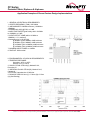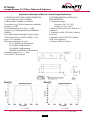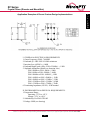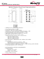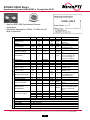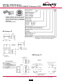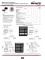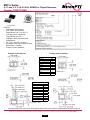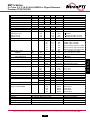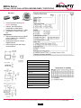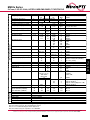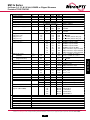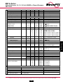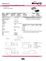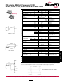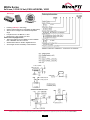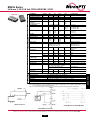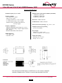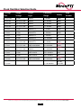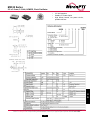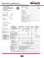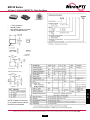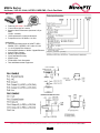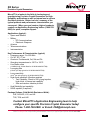
1
MtronPTI...when timing matters MtronPTI offers one of the broadest product portfolios in the Frequency Control & Filter industry. The focus is to supply advanced products and engineering services unmatched in the industry. Products range from crystals (both commercial and precision), clock oscillators, GPSDO, VCXO, TCXO, OCXO and Modular Timing Solutions to various Filter products, including LC, SAW, Ceramic, Crystal, Cavity and Microwave. Customers can essentially get all Frequency Control & Filter devices from MtronPTI. MtronPTI’s commitment to customers in the markets that we serve is unsurpassed. Military and Aerospace, Telecommunications and Commercial Industry customers rely on MtronPTI’s specialized services from design and development to implementation and troubleshooting. Some of the top companies in these fields rely on MtronPTI for all their fequency control and filter needs. Let MtronPTI’s professional and knowledgeable team help you design and implement your next project. MtronPTI Mission Statement MtronPTI creates highly differentiated value through a comprehensive portfolio of custom and standard Frequency Control and Filter products for global markets demanding high reliability, superior cycle times and flexible supply chain capabilities. www.mtronpti.com Table of Contents Filters 4-25 4 5 6-8 10-12 14-17 18-20 22-25 Selection Guide Filter Specification Worksheet Microwave Filters Ceramic Filters Lumped Element (LC) Filters SAW Filters Crystal Filters Global Positioning Satellite Disciplined Oscillators (GPSDO) Selection Guide 1 x 1 inch 1 x 2.5 inch 1.5 x 3 inch 26-35 26 27-29 30-31 32-35 Oven Controlled Crystal Oscillators (OCXO) 36-47 Selection Guide Other 36 37-45 Full Size (14-pin) DIP 46-47 Temperature Compensated Crystal Oscillators (TCXO/TCVCXO) 48-63 Selection Guide 5.0 x 7.0 mm 9 x 14 mm Full Size (14-pin) DIP Other 46 49-57 58-59 37-39 60-63 Voltage Controlled Crystal Oscillators (VCXO) 64-75 Selection Guide 5.0 x 7.0 mm 9 x 14 mm Other 64 65-71 72-73 74 Clock Oscillators 76-97 Selection Guide 2.5 x 3.2 mm 3.2 x 5.0 mm 5.0 x 7.0 mm 9 x 14 mm MIL-PRF-55310 QPL 76 77 78 79-93 94-95 96-97 2 Table of Contents Crystal Products 98-107 98 99-100 101-104 105 106-107 Selection Guide ATS & ATSM-49 Crystals Surface Mount Precision Crystals Qualified Crystals Appendix 108-114 Load Circuit Diagrams Solder Profiles Alphabetical Product Index 108-109 110 112-114 Products that are RoHS compliant as of January 1, 2005 are labeled with this mark: 3 Filter Selection Guide Cavity Filter 0.5% to 10% Bandwidth Combline Filter 10% to 80% Bandwidth Monoblock Ceramic 0.5 to 40% Bandwidth Lumped Element (L-C) 3% to 180% Bandwidth SAW 0.01% to 45% Bandwidth Discrete Crystal 0.01% to 2% Bandwidth Monolithic Crystal 0.014% to 0.5% Bandwidth DC 0.03 0.3 1.6 4 6 8 10 12 18 20 GHz CENTER FREQUENCY MtronPTI’s Filter Capabilities: • • • • • • • • • Bandwidths from 100 Hz to 10 GHz (The bar graph above illustrates where each technology is best utilized in terms of frequency and bandwidth.) Custom design capabilities Commercial, Military and Space capabilities Laser weld capabilities Surface mount applications Lead or RoHS capabilities No pure tin available on request 40+ years of success in the filter market Expertise required to serve as a reliable partner in the most challenging product development environment. Our Application Engineers are available to assist you with your specific filter applications. Just call 407-298-2000 MtronPTI reserves the right to make changes to the product(s) and service(s) described herein without notice. No liability is assumed as a result of their use or application. Please see www.mtronpti.com for our complete offering and detailed datasheets. Contact us for your application specific requirements: MtronPTI 1-800-762-8800. 4 Filter Specifications FON Go to the www.mtronpti.com for the interactive ‘Filter Specifier to define your filter requirements. The following are additional specification points which may be required to properly define your filter. Additional Stopband Points: Stopband 2: Lower ____ MHz/kHz Upper ____ MHz/kHz Stopband 3: Lower ____ MHz/kHz Upper ____ MHz/kHz Group Delay: Absolute: ___[] µsec []ηsec Differential Group Delay: ___[]µsec []ηsec Over Any ___[]MHz []kHz Within the Passband Return Loss: ______ dB minimum Maximum Input Signal Power: __ []Watts []dBm []CW [] Pulsed __ % Duty Cycle Termination Impedance (ZS/ZL): [] 50Ω nominal [] Other ___ Ω // ____ pF Environmental: Vibration: Operating: _________________________________ Non-Operating: _________________________________ Shock: Operating: _________________________________ Non-Operating: _________________________________ Altitude: Operating: _________________________________ Non-Operating: _________________________________ Humidity: [] Condensing [] Non-Condensing Operating: _________________________________ Non-Operating: _________________________________ Application (please describe): ________________________________________________________________ ________________________________________________________________________________________ Contact Information: Company: ______________________________ Street: ___________________________________________ City: ________________ State (Province): _________ Postal Code: _______ Country: _____________ Technical Contact: _________________ (Name) TEL: _______________ eMail: ______________________ Project Name: ____________________________ Prototype Date Required: ________ Quantity _________ Target Price: ________ @ ______ (Qty) Production Date Required: _______ Quantity _________ MtronPTI reserves the right to make changes to the product(s) and service(s) described herein without notice. No liability is assumed as a result of their use or application. Please see www.mtronpti.com for our complete offering and detailed datasheets. Contact us for your application specific requirements: MtronPTI 1-800-762-8800. 5 F I L T E R S UF Series Microwave Filters Product Line Features: • • • • • Highly customized designs for optimum performance using state-of-the-art simulation software. • Allows system optimization for performance size and weight. • Fewer prototype iterations, faster development cycles. Adaptable manufacturing supports commercial, military, avionics and space applications. Laser hermetic packages for severe environments RoHS compliant when required. Available Design topologies • Dielectric Resonator • Cavity • Combline • Interdigital • Helical • Evanescent mode designs Frequency (GHz) Frequency 1 dB % BW VSWR Max. Temperature # of Poles Impedance (Ohms) 100 MHz 15 GHz 100 MHz - 15 GHz 0.5% to Multi-Octave 1.1:1 or better -55°C - +110°C 2-pole to 12-pole 50Ω typical Dielectric Resonator Filters employ ceramic pucks as resonators and, with Q’s in excess of 10,000 readily achievable; this technology is the choice for the narrowest bandwidth requirements. Dielectric resonator filters usually have bandwidths that range from less than 1% to 5%. Cavity Filters employ conductive rods within conductive cavities as resonators. Apertures in the cavity walls permit coupling between resonators. Smaller apertures give narrower filters. Larger cavities have higher Q factors. Cavity filter bandwidths range from less than 3% to 20%. Combline Filters are a close relative to cavity filters. In the Combline design the walls between adjacent cavities are completely removed and coupling between resonators is achieved by designing the correct spacing between resonators. These filters are commonly designed with all resonators in a straight line looking much like a comb. Combline filter bandwidths will range from 5% to 50% Interdigital Filters are similar to Combline filters except the grounded end of alternate resonators is reversed. This arrangement gives the high inter-resonator coupling required for wide filter bandwidths. These filters have bandwidths up to nearly 100%. Helical Filters are used at lower frequencies where resonator length becomes impractically long. The resonator, usually of one quarter wavelength, is coiled into a helix resulting in a much more compact design. Coupling between resonators is managed in the same manner as cavity or combline filters. Bandwidths from 1% to 30% can be achieved. Evanescent Mode is used to describe resonators whose length is short, less than 30 degrees at the frequency of operation. Non-evanescent mode designs will use resonators between 45 and 80 degrees in length. The resultant resonator can be dramatically smaller but has lower Q and is typically more sensitive to manufacturing variations. MtronPTI reserves the right to make changes to the product(s) and service(s) described herein without notice. No liability is assumed as a result of their use or application. Please see www.mtronpti.com for our complete offering and detailed datasheets. Contact us for your application specific requirements: MtronPTI 1-800-762-8800. 6 UF Series Microwave Filters Cavity Dual Band Reject Filter for LTE I. GENERAL & ELECTRICAL REQUIREMENTS: 1. PASSBAND Port C - ANT: 769.15MHz to 770.00MHz ANT – Port B: 799.15MHz to 800.00MHz 2. PASSBAND INSERTION LOSS: 1.7dB typical, 2.0dB maximum 3. PASSBAND VSWR: 1.5:1 maximum 4. STOPBAND REJECTION Port C – ANT (772MHz – 870MHz): 40dB minimum ANT - Port B (772MHz – 776MHz): 40dB minimum ANT - Port B (802MHz – 870MHz): 40dB minimum 5. PORT – PORT ISOLATION Port C – Port B (769.15MHz – 770.00MHz): 70dB min Port C – Port B (799.15MHz – 800.00MHz): 70dB min 6. POWER HANDLING: +37dBm minimum 7. ZIN/ZOUT: 50W nominal II. ENIVIRONMENTAL & PHYSICAL REQUIREMENTS: 1. ENVIRONMENTAL Temperature Operating: -20°C to +60°C Storage: -40°C to +85°C Shock: Per MIL-STD-810F, 516.5, Procedure I Vibration: Per MIL-STD-810F, 514.5, Procedure I Altitude: ≤ 10,000-ft Humidity: Per MIL-STD-810F, 509.4, Procedure II Rain: Per MIL-STD-810F, 506.4, Procedure II Sand & Dust: Per MIL-STD-810F, 510.4, Procedure I 2. PACKAGE Dimensions (maximum, excluding connectors): 10.50” (L) x 9.50” (W) x 2.88” (H) I/O Connectors: N-Female (ANT), TNC-Female (Port B), BNCFemale (Port C) MtronPTI reserves the right to make changes to the product(s) and service(s) described herein without notice. No liability is assumed as a result of their use or application. Please see www.mtronpti.com for our complete offering and detailed datasheets. Contact us for your application specific requirements: MtronPTI 1-800-762-8800. 7 F I L T E R S UF Series Microwave Filters Cavity Filter Diplexer for LTE I. GENERAL & ELECTRICAL REQUIREMENTS: 1. PASSBAND Port C - ANT: 769.15MHz to 770.00MHz ANT – Port B: 799.15MHz to 800.00MHz 2. PASSBAND INSERTION LOSS: 1.7dB typical, 2.0dB max 3. PASSBAND VSWR: 1.5:1 maximum 4. STOPBAND REJECTION Port C – ANT (772MHz – 870MHz): 40dB minimum ANT - Port B (772MHz – 776MHz): 40dB minimum ANT - Port B (802MHz – 870MHz): 40dB minimum 5. PORT – PORT ISOLATION Port C – Port B (769.15MHz – 770.00MHz): 70dB minimum Port C – Port B (799.15MHz – 800.00MHz): 70dB minimum 6. POWER HANDLING: +37dBm minimum 7. ZIN/ZOUT: 50W nominal II. ENIVIRONMENTAL & PHYSICAL REQUIREMENTS: 1. ENVIRONMENTAL Temperature Operating: -20°C to +60°C Storage: -40°C to +85°C Shock: Per MIL-STD-810F, 516.5, Procedure I Vibration: Per MIL-STD-810F, 514.5, Procedure I Altitude: ≤ 10,000-ft Humidity: Per MIL-STD-810F, 509.4, Procedure II Rain: Per MIL-STD-810F, 506.4, Procedure II Sand & Dust: Per MIL-STD-810F, 510.4, Procedure I 2. PACKAGE Dimensions (maximum, excluding connectors): 10.50” (L) x 9.50” (W) x 2.88” (H) I/O Connectors: N-Female (ANT), TNCFemale (Port B), BNC-Female (Port C) MtronPTI reserves the right to make changes to the product(s) and service(s) described herein without notice. No liability is assumed as a result of their use or application. Please see www.mtronpti.com for our complete offering and detailed datasheets. Contact us for your application specific requirements: MtronPTI 1-800-762-8800. 8 F I L T E R S Need Help in your Design? Call us at 1-800-762-8800 MtronPTI reserves the right to make changes to the product(s) and service(s) described herein without notice. No liability is assumed as a result of their use or application. Please see www.mtronpti.com for our complete offering and detailed datasheets. Contact us for your application specific requirements: MtronPTI 1-800-762-8800. 9 CF Series Ceramic Filters, Diplexers & N-plexers Product Line Features: • • • • • Custom design capability Commercial and Military capabilities Discrete monoblock implementations Monoblock based filter assemblies RoHS compliant when required Frequency (GHz) 3 dB % BW VSWR Max. Temperature # of Poles Impedance (Ohms) 300 MHz - 5 GHz 0.5% - 40% 1.5:1 or better -45°C - +85°C 2-pole to 8-pole 50Ω typical Application Examples of Recent Custom Design Implementations I. GENERAL & ELECTRICAL REQUIREMENTS 1. CENTER FREQUENCY (FON): 1815.0MHz typical 2. PASSBAND @ 1.5dB: 1780.0MHz to 1850.0MHz, minimum 3. INSERTION LOSS (1780.0MHz to 1850.0MHz): 1.5dB maximum 4. AMPLITUDE RIPPLE (peak-peak, 1780.0MHz to 1850.0MHz): 0.8dB maximum 5. RETURN LOSS (within 1780.0MHz to 1850.0MHz): 15.0dB minimum 6. ATTENUATION (minimum) @ 1655.0MHz: 20dB minimum @ 1315MHz: 40dB minimum @ 1975MHz: 20dB minimum @ 2315MHz: 40dB minimum 7. ULTIMATE ATTENUATION: 50dB minimum 8. MAXIMUM INPUT POWER:1-Watt 9. ZS/ZL: 50W typical (single ended, no external matching required) II. ENIVIRONMENTAL & PHYSICAL REQUIREMENTS: 1. TEMPERATURE RANGE Operating: -40°C to +70°C Storage: -40°C to +85°C 2. PACKAGE: : See Drawing 3. SOLDERABILITY: Per EIAJ-STD-002 4. FULL RoHS COMPLIANCE MtronPTI reserves the right to make changes to the product(s) and service(s) described herein without notice. No liability is assumed as a result of their use or application. Please see www.mtronpti.com for our complete offering and detailed datasheets. Contact us for your application specific requirements: MtronPTI 1-800-762-8800. 10 CF Series Ceramic Filters, Diplexers & N-plexers Application Examples of Recent Custom Design Implementations I. GENERAL & ELECTRICAL REQUIREMENTS: 1. CENTER FREQUENCY (FON): 1250.0MHz 2. 1dB BANDWIDTH: 280MHz minimum (1110MHz to 1390MHz) 3. INSERTION LOSS (@ FON): ≤ 1.0dB 4. AMPLITUDE RIPPLE (peak-valley, within 1110MHz to 1390MHz): ≤ 1.0dB 5. INPUT/OUTPUT VSWR (within 1110MHz to 1390MHz): 1.5: 1 maximum 6. Attenuation (ref. to IL @ FON) @ 900MHz (FON -350MHz): 60dB minimum @ 950MHz (FON -300MHz): 40dB minimum @ 1650MHz (FON +400MHz): 40dB minimum @ 1850MHz (FON +600MHz): 60dB minimum 7. MAXIMUM INPUT POWER: ≤ +30dBm 8. ZIN/ZOUT: 50W nominal II. ENIVIRONMENTAL & PHYSICAL REQUIREMENTS: 1. TEMPERATURE RANGE: Operating: -40°C to +85°C Storage: -55°C to +90°C 2. SHOCK: Per MIL-STD-810(G), Method 516.6, Procedure VI 3. VIBRATION: Per MIL-STD-810(G), Method 514.6, Category 9 4. ALTITUDE: Operational to 35,000 feet 5. PACKAGE: SMD: 26.0mm (l) x 17.0mm (W) x 5.5mm (H) (See Drawing) MtronPTI reserves the right to make changes to the product(s) and service(s) described herein without notice. No liability is assumed as a result of their use or application. Please see www.mtronpti.com for our complete offering and detailed datasheets. Contact us for your application specific requirements: MtronPTI 1-800-762-8800. 11 F I L T E R S CF Series Ceramic Filters, Diplexers & N-plexers Application Examples of Recent Custom Design Implementations I. GENERAL & ELECTRICAL REQUIREMENTS: 1. CENTER FREQUENCY (FON): 3724MHz 2. BANDWIDTH: FON ± 55MHz minimum (3669MHz to 3779MHz) 3. INSERTION LOSS (@ peak of transmission within the passband): ≤ 4.0dB 4. AMPLITUDE RIPPLE (peak-valley within the passband): ≤ 1.5dB 5. RETURN LOSS (within the passband): 13dB minimum, 15db typical 6. GROUP DELAY VARIATION (over FON ±45MHz): 5.0ηsec typical, 10.0ηsec maximum 7. PHASE DISTORTION (over FON ±45MHz): ±15.0˚ typical, 25.0˚ maximum 8. ATTENUATION (ref. to IL) 10MHz to 3559MHz: 60dB minimum @3589MHz: 42dB minimum @ 3889MHz: 42dB minimum 3889MHz to 6000MHz: 55dB minimum 9. MAXIMUM INPUT POWER: ≤ 1-Watt 10. ZIN/ZOUT: 50Ω nominal II. ENIVIRONMENTAL & PHYSICAL REQUIREMENTS: 1. TEMPERATURE RANGE: Operating: -40°C to +85°C Storage: -55°C to +85°C 2. SHOCK: Per MIL-STD-202G, Method 202C 3. VIBRATION: Per MIL-STD-202G, Method 201A 4. HUMIDITY: Per MIL-STD-202, Method 103B, Test Condition A 5. ALTITUDE: Per MIL-STD-202G, Method 105C, Test Condition A 6. PACKAGE: SMD: See Figure 1 MtronPTI reserves the right to make changes to the product(s) and service(s) described herein without notice. No liability is assumed as a result of their use or application. Please see www.mtronpti.com for our complete offering and detailed datasheets. Contact us for your application specific requirements: MtronPTI 1-800-762-8800. 12 F I L T E R S Need Help in your Design? Call us at 1-800-762-8800 MtronPTI reserves the right to make changes to the product(s) and service(s) described herein without notice. No liability is assumed as a result of their use or application. Please see www.mtronpti.com for our complete offering and detailed datasheets. Contact us for your application specific requirements: MtronPTI 1-800-762-8800. 13 LF Series Lumped Element (LC) Filters, Diplexers & N-plexers Product Line Features: • • • • • • • • Highly customized designs for optimum performance using state-ofthe-art simulation software. • Allows system optimization for performance size and weight. • Fewer prototype iterations, faster development cycles. Adaptable manufacturing supports commercial, military, avionics and space applications. Laser hermetic packages for severe environments RoHS compliant when required. No pure tin assemblies available. Non-vented surface mount filters • Eliminates performance drift through water wash. • Low profile less than 0.200 inches for some applications. Low pass, high pass, Bandpass and notch filters available. Hybrid lumped element and distributed element microwave designs for applications requiring higher Q factors. Frequency (GHz) 3 dB % BW VSWR # of Poles Impedance (Ohms) DC - 5 GHz 3% - 180% 1.5:1 or better Optimized for Selectivity 50Ω typical The following are some additional filter facts and guidelines based upon application type. Operating Temperature Range Packaging Input/Output Signal Power Shock/Vibration Operational & Survival Instrumentation Industrial Communications HiRel Military Space Qualified 0°C to +70°C -20°C to +75° C -30°C to +85°C -55°C to +110°C -55°C to +110°C Thru-Hole Wash Proof SMD Connectorized Hermetic Thru Hole and SMD To 500 Watt (Consult factory for specific high power requirements.) Meet Standard Industry Requirements Consult the Factory for Specific Requirements Allow MtonPTI to work with you in developing your filter requirements. Our design staff, with many years of experience, will evaluate your requirements to give you honest and realistic estimates of achievable performance. We promise to work our hardest, up front, to find the optimal compromise between performance, price, size and reliability for your application. We will provide you with the information you need to advance your design; cost estimates, performance plots, S2p data and packaging recommendations. MtronPTI reserves the right to make changes to the product(s) and service(s) described herein without notice. No liability is assumed as a result of their use or application. Please see www.mtronpti.com for our complete offering and detailed datasheets. Contact us for your application specific requirements: MtronPTI 1-800-762-8800. 14 LF Series Lumped Element (LC) Filters, Diplexers & N-plexers Applications Examples of Recent Custom Design Evaluations I. GENERAL & ELECTRICAL REQUIREMENTS: 1. Center Frequency (FON): Channel 1: 256MHz Channel 2; 305MHz 2. 1dB Bandwidth: Channel 1 28MHz minimum II. ENIVIRONMENTAL & PHYSICAL REQUIREMENTS: Channel 2 26MHz minimum 1. Temperature Range: 3. Insertion Loss (@ FON): ≤ 1.0dB Operating: -40°C to +85°C 4. Amplitude Ripple (peak-valley, Storage: -55°C to +90°C within each Passband): ≤ 0.5dB 2. Shock: Per MIL-STD-810(G), Method 516.6, Procedure VI 5. Return Loss : 20dB minimum 3. Vibration: Per MIL-STD-810(G), Method 514.6, Category 9 6. Attenuation (ref. to IL @ FON) 4. Altitude: Operational to 35,000 feet Channel 1: 256MHz 5. Package: (See Drawing) 35dB minimum: @ 225MHz 35dB minimum: @ 289MHz Channel 2; 305 MHz 35dB minimum: 280MHz 35dB minimum: 330MHz 7. Maximum Input Power: ≤ 50-Watts 8. ZIN/ZOUT: 50Ω nominal MtronPTI reserves the right to make changes to the product(s) and service(s) described herein without notice. No liability is assumed as a result of their use or application. Please see www.mtronpti.com for our complete offering and detailed datasheets. Contact us for your application specific requirements: MtronPTI 1-800-762-8800. 15 F I L T E R S LF Series Lumped Element (LC) Filters, Diplexers & N-plexers Applications Examples of Recent Custom Design Evaluations I. GENERAL & ELECTRICAL REQUIREMENTS: 1. Center Frequency (FON): 2050MHz 2. 2dB Passband: 1600MHz to 2500MHz 3. Insertion Loss (@ peak of transmission within the passband): ≤ 2.0dB 4. Passband Ripple (peak-valley): ≤ 0.5dB 5. Return Loss: 15db minimum from 1600MHz to 2500MHz 6. Passband Group Delay Ripple: 8.0ηsec typical 7. Phase Distortion (over FON ±45MHz): ±15.0˚ typical, 25.0˚ maximum 8. Rejection (minimum, ref. to IL) DC to 1100MHz: 60dB minimum @ 1350MHz: 40dB minimum @ 2900MHz: 40dB minimum 3600MHz to 6000MHz: 60dB minimum 9. Maximum Input Power: ≤ 1-Watt 10. ZIN/ZOUT: 50Ω nominal II. ENIVIRONMENTAL & PHYSICAL REQUIREMENTS: 1. Temperature Range: Operating: -40°C to +110°C Storage: -55°C to +120°C 2. Shock: Per MIL-STD-202G, Method 213, Condition C 3. Vibration: Per MIL-STD-202G, Method 201 & 204 4. Humidity: Per MIL-STD-202, Method 103B, Test Condition A 5. Package: SMD: See Figure 1 MtronPTI reserves the right to make changes to the product(s) and service(s) described herein without notice. No liability is assumed as a result of their use or application. Please see www.mtronpti.com for our complete offering and detailed datasheets. Contact us for your application specific requirements: MtronPTI 1-800-762-8800. 16 LF Series Lumped Element (LC) Filters, Diplexers & N-plexers Typical Package Configurations True SMT (SM) PC Mount (PC) Castellation GW1 &ĂŵŝůLJ 'tϭͲϬϬϭ 'tϭͲϬϬϮ 'tϭͲϬϬϯ 'tϭͲϬϬϰ 'tϭͲϬϬϱ 'tϭͲϬϬϲ Connectorized (C) /D Ϭ͘ϱϬϬ Ϭ͘ϳϱϬ ϭ͘ϬϬϬ ϭ͘ϮϱϬ ϭ͘ϱϬϬ ϭ͘ϳϱϬ MtronPTI reserves the right to make changes to the product(s) and service(s) described herein without notice. No liability is assumed as a result of their use or application. Please see www.mtronpti.com for our complete offering and detailed datasheets. Contact us for your application specific requirements: MtronPTI 1-800-762-8800. 17 F I L T E R S SF Series SAW Filters Product Line Features • • • • • Custom design capability Commercial and Military capabilities IF and low loss RF design capabilities Ceramic SMD and all metal DIL thru-hole packages Lead or RoHS Frequency (GHz) 3 dB % BW Shape Factor Insertion Loss VSWR Temperature # of Poles Impedance (Ohms) 20 MHz 2.5 GHz 0.1% - 10% 1.1:1 and higher 1dB typical 1.1:1 or better -45°C - +85°C 2-pole to 8-pole 50Ω typical Application Examples of Recent Custom Design Implementations I. GENERAL & ELECTRICAL REQUIREMENTS: 1. CENTER FREQUENCY (FON): 915.00MHz typical 2. 3dB BANDWIDTH: 26.0MHz typical 3. INSERTION LOSS: 2.5dB typical, 3.1dB maximum 4. AMPLITUDE RIPPLE (peak-peak):0.4dB typical, 1.5dB maximum 5. GROUP DELAY DEVIATION: 15ηsec typical, 50ηsec maximum 6. RETURN LOSS: 9dB minimum, 10dB typical 7. REJECTION (ref. to 0dB) 0.1MHz to 702MHz: 50dB minimum, 53db typical 738MHz to 764MHz: 49dB minimum, 53dB typical 820MHz to 846MHz: 42dB minimum, 48dB typical 990MHz to 1010MHz: 42dB minimum, 50dB typical 1072MHz to 1092MHz: 49dB minimum, 53db typical 1128MHz to 1804MHz: 40dB minimum, 42dB typical 1804MHz to 1856MHz: 40dB minimum, 42dB typical 1856MHz to 3000MHz: 30dB minimum, 36dB typical 8. INPUT POWER LEVEL: +10dB maximum 9. DC VOLTAGE: +3V maximum 10. ZS/ZL: 50Ω typical (no external matching required) II. ENVIRONMENTAL & PHYSICAL REQUIREMENTS: 1. TEMPERATURE Operating: -30C to +85C Storage: -45°C to +90°C 2. PACKAGE 1.4mm x 1,1mm x 0.7mm (see drawing) 3. SOLDERABILITY: Per EIAJ-STD-002 4. FULL RoHS COMPLIANCE MtronPTI reserves the right to make changes to the product(s) and service(s) described herein without notice. No liability is assumed as a result of their use or application. Please see www.mtronpti.com for our complete offering and detailed datasheets. Contact us for your application specific requirements: MtronPTI 1-800-762-8800. 18 SF Series SAW Filters Application Examples of Recent Custom Design Implementations I. GENERAL & ELECTRICAL REQUIREMENTS: 1. CENTER FREQUENCY (FON): 243.00MHz typical 2. PASSBAND: FON ± 25.0MHz minimum 3. INSERTION LOSS (IL): 3.7dB typical, 6.0dB maximum 4. AMPLITUDE RIPPLE (peak-peak): 0.2dB typical, 1.0dB maximum 5. GROUP DELAY VARIATION: 0.5msec typical, 2.0msec maximum 6. ATTENUATION (ref. to minimum IL) FON - 115.0MHz to FON - 1.0MHz: 50dB minimum, 63dB typical FON - 1.0MHz to FON - 0.6MHz: 42dB minimum, 64dB typical FON - 0.6MHz to FON - 0.4MHz: 29dB minimum, 68dB typical FON + 0.4MHz to FON + 0.6MHz: 29dB minimum, 64dB typical FON + 0.6MHz to FON + 1.0MHz: 42dB minimum, 63dB typical FON + 1.0MHz to FON + 115MHz: 50dB minimum, 55dB typical 7. MAXIMUM INPUT POWER:+15dBm 8. ZIN/ZOUT: 50W typical (with external matching network applied) II. ENIVIRONMENTAL & PHYSICAL REQUIREMENTS: 1. TEMPERATURE RANGE OPERATING: -40°C to +85°C OPERATING: -45°C to +90°C 2. PACKAGE See Drawing 3. SOLDERABILITY: Per EIAJ-STD-002 (see Figure 1) 4. FULL RoHS COMPLIANCE MtronPTI reserves the right to make changes to the product(s) and service(s) described herein without notice. No liability is assumed as a result of their use or application. Please see www.mtronpti.com for our complete offering and detailed datasheets. Contact us for your application specific requirements: MtronPTI 1-800-762-8800. 19 F I L T E R S SF Series SAW Filters Application Examples of Recent Custom Design Implementations I. GENERAL & ELECTRICAL REQUIREMENTS: 1. CENTER FREQUENCY (FON) @ 25°C: 408.875MHz minimum, 409.0MHz typical, 409.125MHz maximum 2. INSERTION LOSS (@ peak of transmission within the passband): <12.0dB 3. AMPLITUDE RIPPLE (peak-peak, within the passband): <0.75dB 4. BANDWIDTH @ 1dB: >0.6MHz @ 3dB: >1.0MHz @40dB: <3.0MHz 5. PHASE LINEARITY (over 408.6MHz to 409.4MHz): <6° 6. GROUP DELAY VARIATION (over 408.6MHz to 409.4MHz): < 250hsec 7. STOPBAND REJECTION Over 200.0MHz to 369.0MHz: > 50dB Over 449.0MHz to 600.0MHz: > 50dB 8. AMBIENT TEMPERATURE: 25°C typical 9. MAXIMUM INPUT SIGNAL POWER: +10dBm 10. ZS/ZL: 50Ω nominal II. ENIVIRONMENTAL & PHYSICAL REQUIREMENTS: 1. OPERATING TEMPERATURE RANGE: -40°C to +80°C 2. VIBRATION Random Vibration - Band: 20 to 2000Hz - Level: 30geff, s = 3 - Duration: 3-minutes per axe - One try by axe: 3-axes Long Term Random Vibration Level: 5.3geff Duration: 2-hours 30-minutes per axe – 3 axes 3. ACCELERATION Level: 100g Duration: 3-minutes by direction 3 axes – 6 directions 4. HYGROSCOPY (HUMIDITY) Temperature: +40°C Humidity: 93% ±2% Duration: 10-hours 5. THERMAL SHOCK The filter is placed in a confined room at 60°C during 5-hours then placed in another confined room at 150°C during 3-min. Control are made during the thermal shock: transmission curve MtronPTI reserves the right to make changes to the product(s) and service(s) described herein without notice. No liability is assumed as a result of their use or application. Please see www.mtronpti.com for our complete offering and detailed datasheets. Contact us for your application specific requirements: MtronPTI 1-800-762-8800. 20 F I L T E R S Need Help in your Design? Call us at 1-800-762-8800 MtronPTI reserves the right to make changes to the product(s) and service(s) described herein without notice. No liability is assumed as a result of their use or application. Please see www.mtronpti.com for our complete offering and detailed datasheets. Contact us for your application specific requirements: MtronPTI 1-800-762-8800. 21 XF Series Crystal Filters (Discrete and Monolithic) Product Line Features • • • • • • Custom design capability Commercial, Military and Space capabilities Monolithic and Discrete design capability Wash proof for surface mount applications Lead or RoHS No pure tin available upon request Type Frequency (MHz) 3 dB % BW Shape Factor Insertion Loss VSWR Max. Temperature # of Poles Impedance (Ohms) Discrete 5 - 250 0.01% - 2% 1.5:1 or better 1.5 dB for 2-pole 1.5:1 or better -45°C - +85°C 2-pole to 12-pole 50Ω typical Monolithic 5 - 200 0.014% - 0.5% 2:1 or better 1.5 dB for 2-pole 1.5:1 or better -45°C - +85°C 2-pole to 12-pole 50Ω typical The following are some additional filter facts and guidelines based upon application type. Operating Temperature Range Packaging Input/Output Signal Power Shock/Vibration Operational & Survival Instrumentation Industrial Communications HiRel Military Space Qualified 0°C to +70°C -20°C to +75° C -30°C to +85°C -55°C to +110°C -55°C to +110°C Thru-Hole Wash Proof SMD Connectorized Hermetic Thru Hole and SMD <+15dBm (Consult factory for specific requirements.) Meet Standard Industry Requirements Consult the Factory for Specific Requirements Allow MtonPTI to work with you in developing your filter requirements. Our design staff of many years’ experience will evaluate your requirements and give you realistic estimates of achievable performance. We will work our hardest to find the optimal compromise between performance, price, size and reliability for your application. We will provide you with the information you need to advance your design; cost estimates, performance plots, S2p data and packaging recommendations. MtronPTI reserves the right to make changes to the product(s) and service(s) described herein without notice. No liability is assumed as a result of their use or application. Please see www.mtronpti.com for our complete offering and detailed datasheets. Contact us for your application specific requirements: MtronPTI 1-800-762-8800. 22 XF Series Crystal Filters (Discrete and Monolithic) Application Examples of Recent Custom Design Implementations I. GENERAL & ELECTRICAL REQUIREMENTS 1. Center Frequency (FON): 76.0MHz 2. Passband @ 1.5dB: FON ±25.0kHz minimum 3. Insertion Loss (@FON): ≤ 4.0dB 4. Passband Ripple (peak-valley, FON ±25.0kHz): < 1.5dB 5. Stopband Attenuation (Relative to Insertion Loss) FON -50MHz to FON -1MHz: ≥ 50dB FON -1MHz to FON -500kHz: ≥ 40dB FON -500kHz to FON -100kHz: ≥ 15dB FON +100kHz to FON +500kHz: ≥ 15dB FON +500kHz to FON +2.5MHz: ≥ 35dB FON +2.5MHz to FON +3.5MHz: ≥ 45dB FON +3.5MHz to FON +75MHz: ≥ 50dB 6. Terminating Impedance (ZS/Z/L): 50W nominal II. ENVIRONMENTAL & PHYSICAL REQUIREMENTS: 1. Temperature Range Operating: -55°C to +85°C Storage: -55°C to +90°C 2. Solderability: Per EIAJ-STD-002 3. Package: SMD (see drawing) MtronPTI reserves the right to make changes to the product(s) and service(s) described herein without notice. No liability is assumed as a result of their use or application. Please see www.mtronpti.com for our complete offering and detailed datasheets. Contact us for your application specific requirements: MtronPTI 1-800-762-8800. 23 F I L T E R S XF Series Crystal Filters (Discrete and Monolithic) Application Examples of Recent Custom Design Implementations I. GENERAL & ELECTRICAL REQUIREMENTS 1. Center Frequency (FON): 112.5MHz 2. Passband @ 1.0dB: FON ±10.0kHz minimum 3. Insertion Loss (@ peak of transmission, within the Passband): ≤ 4.5dB 4. Passband Ripple (peak-valley, within the Passband): < 0.75dB 5. Input/Output VSWR (within FON ±10.0kHz): 2.2:1 maximum 6. Differential Group Delay (FON ±10.0kHz): ≤8µsec 7. Stopband Attenuation (minimum relative to Insertion Loss) 13dB: FON ±50kHz maximum 28dB: FON ±100kHz maximum 44dB: FON ±400kHz maximum 8. Spurious Responses:- 28dB maximum, FON +100kHz to FON +400kHz 9. Power Handing Operating (full specifications compliance): +7dBm Without Damage (non-specification compliant): +18dBm 10. In-band Intermodulation: -50dB maximum, Two (2) -3.5dBm Test Tones @ FON ±500.0kHz 11. Terminating Impedance (ZS/Z/L): 50W nominal II. ENVIRONMENTAL & PHYSICAL REQUIREMENTS: 1. Temperature Range Operating: -55°C to +85°C Storage: -55°C to +90°C 2. Solderability: Per EIAJ-STD-002 3. Package: SMD (see drawing) MtronPTI reserves the right to make changes to the product(s) and service(s) described herein without notice. No liability is assumed as a result of their use or application. Please see www.mtronpti.com for our complete offering and detailed datasheets. Contact us for your application specific requirements: MtronPTI 1-800-762-8800. 24 XF Series Crystal Filters (Discrete and Monolithic) All package styles except for vented surface mount are hermetic and are available in standard or customized versions. Styles include: • Through hole printed circuit • Connectorized • Stud mount or insert mount • Gull wing surface mount • Vented surface mount The following is an example of MtronPTI’s standard SMD packages suitable for all commercial, industrial and most military applications. MtronPTI reserves the right to make changes to the product(s) and service(s) described herein without notice. No liability is assumed as a result of their use or application. Please see www.mtronpti.com for our complete offering and detailed datasheets. Contact us for your application specific requirements: MtronPTI 1-800-762-8800. 25 F I L T E R S GPSDO Selection Guide Package Size Supply Voltage Frequency Range Family Type 1 x 1 inch 3.3 Volt 10 - 10 MHz M9107 GPSDO 1 x 1 inch 3.3 Volt 10 - 10 Mhz M9108 GPSDO 1 x 2.5 inch 12 Volt 10 - 10 MHz M9100 GPSDO 1.5 x 3 inch 12 Volt 5 - 20 MHz M9101 GPSDO 1.5 x 3 inch 12 Volt 10 - 10 MHz M9103 GPSDO Page Number MtronPTI reserves the right to make changes to the product(s) and service(s) described herein without notice. No liability is assumed as a result of their use or application. Please see www.mtronpti.com for our complete offering and detailed datasheets. Contact us for your application specific requirements: MtronPTI 1-800-762-8800. 26 M9107 Series 1 x 1 x 0.5 inches, SMT OCXO-Based GPSDO (Global Positioning Satellite Disciplined Oscillator) • • • • Small, SMT configuration Direct mounting to PCB eliminates need for expensive connectors and wiring harnesses Ideal for precise timing or locating applications such as test equipment, base stations, network timing and military programs Compact size - less than 1” x 1” Pin Connections Function Pin Ground 1 10 MHz Out 2 Lock OK 3 1PPS Output 4 1PPS Input 5 +5V Output 6 Ground 7 +3.3V VDO In 8 Ground 9 Antenna Input 10 Ground 11 NMEA Transmit 12 /Enter ISP 13 Serial Input 14 Serial Output 15 G P S D O Marking: Line 1: Part Number Line 2: MTRONPTI Line 3: ● Date Code Module Specifications (Typical): 1 PPS Accuracy Holdover Stability 1 PPS Output (OCXO Flywheel Generated) RS-232 Control GPS Frequency GPS Antenna GPS Receiver Sensitivity TTFF ADEV TTL Alarm Output Warm Up Time / Stabilization Time Supply Voltage (Vdd) Power Consumption Operating Temperature Storage Temperature Additional Features Oscillator Specification: Frequency Output 10MHz Retrace Frequency Stability Over Temperature (Unlock Condition) Output Amplitude Warm Up Time M9107 ±40ns to UTC RMS (1-Sigma) GPS Locked (no motion, stable temperature, still air) <±11us over 3 Hour Period @+25°C (No Motion, Still air) 3.3VDC CMOS SCPI-99 TTL levels GPS NMEA Out L1, C/A 1574MHz Active or Passive 50 Channels, Mobile, WAAS, EGNOS, MSAS capable Acquisition –142 dBm, Tracking -158 dBm Cold Start - <45 sec, Warm Start – 1 sec, Hot Start - 1 sec 1E-11 (Tau=1s), <5E-12 (Tau-10,000s) GPS Unlock and Hardware Failure, and LOCK indicators <5 min at +25°C to 1E-08 Accuracy 3.3 V Single Supply (5V internally generated) 0.7W Typical -20°C to +70°C -45°C to +85°C Firmware field-upgradable, external 1PPS input, status LEDs, compatible to GPSCon, SNTP, GPSD, and Z38xx software applications, full NMEA 1Hz 10Hz 100Hz 1kHz 10kHz Phase Noise 10MHz ±2E-08 After 1 Hour 100ppb pk-pk 5.0V CMOS < 1 min @ +25°C -80dBc/Hz -110dBc/Hz -135dBc/Hz -145dBc/Hz <-145dBc/Hz MtronPTI reserves the right to make changes to the product(s) and service(s) described herein without notice. No liability is assumed as a result of their use or application. Please see www.mtronpti.com for our complete offering and detailed datasheets. Contact us for your application specific requirements: MtronPTI 1-800-762-8800. 27 M9108 Series 1 x 1 inches, SMT TCXO-Based GPSDO (Global Positioning Satellite Disciplined Oscillator) • • • • • • Fast Warm-Up Time Extremely Low Power Small, SMT configuration Direct mounting to PCB - eliminates need for expensive connectors and wiring harnesses Ideal for precise timing or locating applications such as test equipment, base stations, network timing and military programs Compact size - less than 1” x 1”, low profile version available Module Specifications (Typical): 1 PPS Accuracy Holdover Stability 1 PPS Output (OCXO Flywheel Generated) RS-232 Control GPS Frequency GPS Antenna GPS Receiver Sensitivity TTFF ADEV TTL Alarm Output Warm Up Time / Stabilization Time Supply Voltage (Vdd) Power Consumption Operating Temperature Storage Temperature Additional Features Oscillator Specification: Frequency Output 10MHz Retrace Frequency Stability Over Temperature (Unlock Condition) Output Amplitude Warm Up Time M9108 ±50ns to UTC RMS (1-Sigma) GPS Locked (No motion, stable temperature, still air) <±11us over 3 Hour Period @+25°C (No Motion, Still air) 3.3VDC CMOS SCPI-99 TTL levels GPS NMEA Out L1, C/A 1574MHz Active or Passive 50 Channels, Mobile, WAAS, EGNOS, MSAS capable Acquisition –142 dBm, Tracking -158 dBm Cold Start - <45 sec, Warm Start – 1 sec, Hot Start - 1 sec 3E-10 (Tau=1s), <9E-12 (Tau-10,000s) GPS Unlock and Hardware Failure, and LOCK indicators <5 min at +25°C to 1E-08 Accuracy 3.3 V Single Supply (5V internally generated) 0.7W Typical -20°C to +70°C -45°C to +85°C Firmware field-upgradable, external 1PPS input, status LEDs, compatible to GPSCon, SNTP, GPSD, and Z38xx software applications, full NMEA 1Hz 10Hz 100Hz 1kHz 10kHz Phase Noise 10MHz ±2E-08 After 1 Hour 100ppb pk-pk 5.0V CMOS < 1 min @ +25°C -80dBc/Hz -110dBc/Hz -135dBc/Hz -145dBc/Hz <-145dBc/Hz MtronPTI reserves the right to make changes to the product(s) and service(s) described herein without notice. No liability is assumed as a result of their use or application. Please see www.mtronpti.com for our complete offering and detailed datasheets. Contact us for your application specific requirements: MtronPTI 1-800-762-8800. 28 M9108 Series 1 x 1 inches, SMT TCXO-Based GPSDO (Global Positioning Satellite Disciplined Oscillator) M9108L Low Profile M9108D DIP G P S D O MtronPTI reserves the right to make changes to the product(s) and service(s) described herein without notice. No liability is assumed as a result of their use or application. Please see www.mtronpti.com for our complete offering and detailed datasheets. Contact us for your application specific requirements: MtronPTI 1-800-762-8800. 29 M9100 Series 1 x 2.5 x 0.5 inch GPSDO (Global Positioning Satellite Disciplined Oscillator) • • • • • 1 x 2.5 x 0.5 Inch Package < 1 Minute OCXO Warm Up 50 Channel WAAS GPS Receiver Very low power (1.35 W typ.) Applications: Fixed/Mobile Communications, Man-Pack Radios, Smart Weapons Module Specification (Typical): 1 PPS Accuracy Holdover Stability 1 PPS Output RS-232 Control GPS Frequency GPS Antenna GPS Receiver Sensitivity TTFF ADEV TTL Alarm Output Warm Up Time / Stabilization Time Supply Voltage (Vdd) Power Consumption Operating Temperature Storage Temperature M9100 ±40ns to UTC RMS (1-Sigma) GPS Locked (no motion, stable temperature, still air) <±11us over 3 Hour Period @+25°C (No Motion) 3.3VDC CMOS Compatible SCPI-99 Control Commands 1PPS Level Output for Linux SNTP Server Software (with D Sub RTS pin) L1, C/A 1574MHz (Gallileo supported when available) Active or Passive 50 Channels, Mobile, WAAS, EGNOS, MSAS capable Acquisition –144 dBm, Tracking -160 dBm Cold Start - <45 sec, Warm Start – 1 sec, Hot Start - 1 sec 2 E-011/1s GPS Unlock and Hardware Failure, and LOCK indicators <5 min at +25°C to 1E-08 Accuracy +7.5 to 14.0 VDC±5% (12 VDC Nominal) <1.8W Max, 1.35W Typ. 0°C to +60°C -45°C to +85°C Oscillator Specification: Frequency Output Retrace Frequency Stability Over Temperature (Unlock Condition) Output Amplitude OCXO Warm Up Time Phase Noise Connections: 1PPS Output, 10MHz Output RS-232 10MHz ±2E-08 After 1 Hour ±2.5E-08 +13dBm ± 3dBm (Refer to user manual for pin out information) < 1 min 1Hz -80dBc/Hz 10Hz -110dBc/Hz 100Hz -135dBc/Hz 1kHz -145dBc/Hz 10kHz <-145dBc/Hz Connector Type: SMB 3 Pin MtronPTI reserves the right to make changes to the product(s) and service(s) described herein without notice. No liability is assumed as a result of their use or application. Please see www.mtronpti.com for our complete offering and detailed datasheets. Contact us for your application specific requirements: MtronPTI 1-800-762-8800. 30 M9100 Series 1 x 2.5 x 0.5 inch GPSDO (Global Positioning Satellite Disciplined Oscillator) G P S D O MtronPTI reserves the right to make changes to the product(s) and service(s) described herein without notice. No liability is assumed as a result of their use or application. Please see www.mtronpti.com for our complete offering and detailed datasheets. Contact us for your application specific requirements: MtronPTI 1-800-762-8800. 31 M9101 Series 1.5 x 3.0 x 0.8 inches, GPSDO (Global Positioning Satellite Disciplined Oscillator) • • • • • • Module Specification (Typical): 1 PPS Accuracy Holdover Stability (After 3 day of lock to GPS) 1 PPS Output 10 MHz Output RS-232 Control GPS Frequency GPS Antenna GPS Receiver GPS Receiver Sensitivity TTFF ADEV TTL Alarm Output OCXO Warm-Up Time/Stabilization Time GPSDO Lock Time to <5E-010 accuracy Supply Voltage Power Consumption Operating Temperature Storage Temperature M9101S (Single Oven) M9101D (Double Oven) 1.5 x 3.0 x 0.8 Inch Package Excellent Holdover Stability Ruggedized Military Low G-Sensitivity Option Available Applications: Master Clock & Receiver for CDMA, WiMAX & GSM Basestations, SATCOM, Precision Time Base Reference (1PPS), and Navigation Systems M9101S (Single Oven Version) M9101D (Double Oven Version) ±25ns to UTC RMS (1-Sigma) GPS Locked ±15ns to UTC RMS (1-Sigma) GPS Locked (no motion, stable temperature, still air) (no motion, stable temperature, still air) < ± 50 µs over 24 hr. period @ +25°C < ± 7 µs over 24 hr. period @ +25°C LVDS compatible LVDS and HCMOS compatible RS-232 Levels. SCPI-99 Control Commands 1 PPS output level for Linux SNTP Server Softrware with D Sub RTS pin. L1, C/A 1574 MHz (Gallileo supported when available) Active or Passive Type 50 channels, Mobile, WAAS, EGNOS, MSAS, capable Acquisition -144 dBm, tracking -160 dBm Cold Start: < 45 sec Warm Start: 1 sec. Hot Start: 1 sec < 1 E -011/1 sec. < 4 E -012/1 sec. GPS Unlock and Hardware Failure Status < 12 min. at +25°C for 1 E-09 accuracy. <1Hr <30 min. 12.0 VDC ± 5% < 2.5 W at 12 V and +25°C < 4.0 W at 12 V and +25°C 0°C to +60°C 0°C to +75°C -45°C to +85°C OCXO Specification: Output Frequency Retrace Frequency Stability Over Operating Temperature Output Amplitude OCXO Retrace time Phase Noise CONNECTIONS: 1 PPS Output, 10 MHz Output, RS-232 Control 10 MHz (Other frequencies 5-20 MHz available) ± 2 E-08 after 1 hr. ± 2.5 E -8 (Unlocked Condition) ± 2.5 E -10 (Unlocked Condition) 5 V HCMOS, LVDS ± 30 mV differential (Refer to user manual for pin out information) < 3Hrs < 1Hr 1 Hz -85 dBc/Hz 1 Hz -90 dBc/Hz 10 Hz -115 dBc/Hz 10 Hz -120 dBc/Hz 100 Hz -140 dBc/Hz 100 Hz -140 dBc/Hz 1 kHz -150 dBc/Hz 1 kHz -150 dBc/Hz 10 kHz -158 dBc/Hz 10 kHz -158 dBc/Hz 16 pin double row header with 2 mm pin spacing MtronPTI reserves the right to make changes to the product(s) and service(s) described herein without notice. No liability is assumed as a result of their use or application. Please see www.mtronpti.com for our complete offering and detailed datasheets. Contact us for your application specific requirements: MtronPTI 1-800-762-8800. 32 M9101 Series 1.5 x 3.0 x 0.8 inches, GPSDO (Global Positioning Satellite Disciplined Oscillator) G P S D O Phase Noise Plot - M9101D (Double Oven) Phase Noise Plot - M9101S (Single Oven) MtronPTI reserves the right to make changes to the product(s) and service(s) described herein without notice. No liability is assumed as a result of their use or application. Please see www.mtronpti.com for our complete offering and detailed datasheets. Contact us for your application specific requirements: MtronPTI 1-800-762-8800. 33 M9103 Series 1.5 x 3.0 x 0.8 inches, GPSDO (Global Positioning Satellite Disciplined Oscillator) With 3-Port Distribution Amplifier • • • • • Module Specification (Typical): 1 PPS Accuracy Frequency Stability Holdover Stability ADEV (Allan Deviation) 1 PPS Output 10 MHz Output 1.5 x 3.0 x 0.8 Inch Package Built-in 10 MHz Distribution Amplifier with 3 Isolated Sinewave Outputs Excellent Holdover Stability Double OCXO with SC-Cut Crystal Applications Requiring Multiple Outputs: Master Clock & Receiver for CDMA, WiMAX & GSM Basestations, SATCOM, Precision Time Base Reference (1PPS), and Navigation Systems M9103S M9103D ±25ns to UTC RMS (1-Sigma) GPS Locked (no motion, stable temperature, still air) ±15ns to UTC RMS (1-Sigma) GPS Locked (no motion, stable temperature, still air) -10 < ± 50 µs over 24 hr. period @ +25°C < 1 E -011/1 sec LVDS compatible LVDS and HCMOS compatible Distribution Amplifier Port Isolation RS-232 Control GPS Frequency GPS Antenna GPS Receiver GPS Receiver Sensitivity TTFF TTL Alarm Output Warm Up Time / Stabilization Time Supply Voltage (Vdd) Power Consumption Operating Temperature Storage Temperature RS-232 Levels. SCPI-99 Control Commands 1 PPS output level for Linux SNTP Server Softrware with D Sub RTS pin. L1, C/A 1574 MHz (Gallileo supported when available) Active or Passive Type 50 channels, Mobile, WAAS, EGNOS, MSAS, capable Acquisition -144 dBm, tracking -160 dBm Cold Start: <45sec. Warm Start: 1 sec. Hot Start: 1 sec. GPS Unlock and Hardware Failure Status < 12 min. at +25°C for 1 E-09 accuracy. 12.0 VDC ± 5% < 2.5 W at 12 V and +25°C 0°C to +60°C -45°C to +85°C Better than ± 3 X 10 after 3 hrs. operation with GPS lock < ± 7 µs over 24 hr. period at +25°C. (No Motion) -11 0.1 s to 1000 s: < 1 X 10 with GPS lock. LVDS Output, RS-232 level output Two LVDS, and three islolated sine wave at +13 dBM, ± 3 dBm 2 MHz: > 98 dB. 10 MHz: > 92 dB. 1 GHz: >92 dB. Full control via SCPI-99 control commands. L1, C/A 1574MHz Passive, or Active (5 V) 50 Channels, Mobile, WAAS, EGNOS, MSAS supported, Galileo ready. Acquisition –144 dBm, Tracking -160 dBm Cold Start - <45 sec, Warm Start – 1 sec, Hot Start - 1 sec GPS Unlock and Hardware Failure indicators -9 < 10 min at +25°C to 1 X 10 accuracy typical + 12 VDC ± 5% Nominal < 4 W Max. at +25°C 0°C to +75°C (-25°C to +75°C available) -45°C to +85°C Oscillator Specification: Frequency Output Retrace Frequency Stability Over Temperature (Unlock Condition) Output Amplitude 10 MHz (Other frequencies 5-20 MHz available) ± 2 E-08 after 1 hr. ± 2.5 E -8 (Unlocked Condition) 5 V HCMOS, LVDS ± 30 mV differential (Refer to user manual for pin out information) 10MHz -8 ± 2 X 10 After 1 Hour -10 ± 2.5 X 10 Sine wave: +13 dBm, ± 3 dBm, LVDS at ± 300 mV Warm Up Time Phase Noise < 12 min 1 Hz -85 dBc/Hz 10 Hz -115 dBc/Hz 100 Hz -140 dBc/Hz 1 kHz -150 dBc/Hz 10 kHz -158 dBc/Hz 1Hz 10Hz 100Hz 1kHz 10kHz Design Lifetime -90 dBc/Hz -135 dBc/Hz -145 dBc/Hz -150 dBc/Hz <-155 dBc/Hz > 10 years MtronPTI reserves the right to make changes to the product(s) and service(s) described herein without notice. No liability is assumed as a result of their use or application. Please see www.mtronpti.com for our complete offering and detailed datasheets. Contact us for your application specific requirements: MtronPTI 1-800-762-8800. 34 M9103 Series 1.5 x 3.0 x 0.8 inches, GPSDO (Global Positioning Satellite Disciplined Oscillator) With 3-Port Distribution Amplifier G P S D O MtronPTI reserves the right to make changes to the product(s) and service(s) described herein without notice. No liability is assumed as a result of their use or application. Please see www.mtronpti.com for our complete offering and detailed datasheets. Contact us for your application specific requirements: MtronPTI 1-800-762-8800. 35 OCXO and DOCXO Selection Guide Package Size Supply Voltage Output Logic Frequency Range 1 x 0.87 inch 5 to 15 Volt HCMOS/Sinewave 10 - 100 MHz XO5180 1 x 0.87 inch 3.3 Volt Synchronous Ethernet HCMOS 10 - 20 MHz XO51841588 1 x 1 inch 3.3 Volt Synchronous Ethernet HCMOS 10 - 20 MHz XO50841588 1 x 1 inch 5 Volt HCMOS/Sinewave 3 - 100 MHz XO5080 1.4 x 1 inch 12 Volt Sinewave (DOCXO) 10 MHz XO5153 1.4 x 1 inch 3.3 to 12 Volt HCMOS/Sinewave 10 - 100 MHz XO5120 1.4 x 1 inch 12 Volt Sinewave 50 - 160 MHz XO5125 14 pin DIP 5.0 Volt HCMOS/TTL 10 - 20 MHz XO5160 14 pin DIP 12.0 Volt HCMOS/TTL 10 - 20 MHz XO5161 14 pin DIP 5.0 Volt Sinewave 10 - 20 MHz XO5162 14 pin DIP 12.0 Volt Sinewave 10 - 20 MHz XO5163 14 pin DIP 3.3 Volt HCMOS 10 - 20 MHz XO5164 Family Page Number MtronPTI reserves the right to make changes to the product(s) and service(s) described herein without notice. No liability is assumed as a result of their use or application. Please see www.mtronpti.com for our complete offering and detailed datasheets. Contact us for your application specific requirements: MtronPTI 1-800-762-8800. 36 XO5180 Series 1x0.87 inch, 5.0 Volt, HCMOS or Sinewave, OCXO • Surface mount package offering both AT and SC-cut crystals • Ideal for microwave radios (short haul), base stations and test equipment applications where size and package style (SMT) are critical O C X O Pin Numbers shown for reference only. Dimemsions are in inches (mm). MtronPTI reserves the right to make changes to the product(s) and service(s) described herein without notice. No liability is assumed as a result of their use or application. Please see www.mtronpti.com for our complete offering and detailed datasheets. Contact us for your application specific requirements: MtronPTI 1-800-762-8800. 37 XO5184-1588-R Series Synchronous Ethernet HCMOS SMT or Through Hole OCXO Parameter Frequency Range Initial Accuracy Symbol F Min. 10.000 Max. 20.000 Units MHz FI -0.5 +0.5 ppm -4.6 +4.6 ppm ∆FT/F -10 +10 ppb ∆FVDD/F -2 +2 ppb Overall vs Temperature vs Supply Voltage 1 x 10 Holdover/Day Output Type Output Load Symmetry (duty cycle) Rise/Fall Time Typ. -11 Short Term Stability Electrical Specifications • Ideal for IEEE-1588 Synchronized Ethernet Applications Specifically designed for 10 MHz, 12.8 MHz and 20 MHz Frequencies -1 TDC TR/TF Logic “1” Level VOH Logic “0” Level VOL 40 HCMOS 15 50 per sec. -10 Storage Temperature Operating Voltage TS VDD -45 3.135 3.3 @ 25°C at time of shipment Over 20 years Over operating temperature range 5% change in voltage Allan Deviation Tau = 1 sec. Constant voltage and load; <±3%°C change in 24 hours after 30 days of continuous operation ppb 60 10 pF % ns @ 50% of waveform From 10% to 90% VOUT V HCMOS Load 10% VDD TA Conditions +1 90% VDD Operating Temperature V HCMOS Load +70 °C Other temperature ranges are available, please contact the factory +85 3.465 °C V Mechanical Shock Vibration Hermeticity Solderability Soldering Conditions Steady state @ 25°C in still air 3.5 Watts @ warm-up Time to be within ±0.1 ppm of the frequency after 3 Minutes 1 hour of operation @ 25°C -130 dBc/Hz 100 Hz -145 dBc/Hz 1 kHz -150 dBc/Hz 10 kHz -150 dBc/Hz 100 kHz Per MIL-STD-202, Method 213, (2000 g’s, 0.3 ms duration, ½ sinewave) Per MIL-STD-202, Method 201 & 204 (10 g’s from 20-2000 Hz) Per MIL-STD-202, Method 112, Test Condition D Per EIAJ-STD-002 See solder profile RoHS Full RoHS 6 Compliance Power Consumption Warm-up Time (Restabilization) Phase Noise (typical) Environmental • 1.25 Watts MtronPTI reserves the right to make changes to the product(s) and service(s) described herein without notice. No liability is assumed as a result of their use or application. Please see www.mtronpti.com for our complete offering and detailed datasheets. Contact us for your application specific requirements: MtronPTI 1-800-762-8800. 38 XO5184-1588-R Series Synchronous Ethernet HCMOS SMT or Through Hole OCXO SMT Package Please contact the factory for other surface mount configurations. Pin Function Part Marking 1 N/C Line 1 MtronPTI 2 N/C Line 2 XO5184-1588 3 Supply Voltage Line 3 Frequency 4 RF Output Line 4 Serial Number 5 N/C Line 5 YYWW 6 N/C 7 Case Ground Suggested Solder Pad Layout Through Hole Package Pin Part Marking Function 1 Vtune 2 N/C 3 N/C Line 1 MtronPTI Line 2 XO5184-1588 7 Vref Line 3 Frequency 8 Ground Line 4 Serial Number 9 Ground Line 5 YYWW 10 RF Output 16 Supply MtronPTI reserves the right to make changes to the product(s) and service(s) described herein without notice. No liability is assumed as a result of their use or application. Please see www.mtronpti.com for our complete offering and detailed datasheets. Contact us for your application specific requirements: MtronPTI 1-800-762-8800. 39 O C X O XO5084-1588-R Series Synchronous Ethernet HCMOS SMT or Through Hole OCXO Parameter Frequency Range Initial Accuracy Symbol F Min. 10.000 Max. 20.000 Units MHz FI -0.5 +0.5 ppm -4.6 +4.6 ppm ∆FT/F -10 +10 ppb ∆FVDD/F -2 +2 ppb Overall vs Temperature vs Supply Voltage 1 x 10 Holdover/Day Output Type Output Load Symmetry (duty cycle) Rise/Fall Time Typ. -11 Short Term Stability Electrical Specifications • Ideal for IEEE-1588 Synchronized Ethernet Applications Specifically designed for 10 MHz, 12.8 MHz and 20 MHz Frequencies -1 TDC TR/TF 40 HCMOS 15 50 per sec. VOH Logic “0” Level VOL Operating Temperature TA -10 Storage Temperature Operating Voltage TS VDD -45 3.135 3.3 Conditions @ 25°C at time of shipment Over 20 years Over operating temperature range 5% change in voltage Allan Deviation Tau = 1 sec. Constant voltage and load; <±3%°C change in 24 hours after 30 days of continuous operation +1 ppb 60 10 pF % ns @ 50% of waveform From 10% to 90% VOUT V HCMOS Load 10% VDD V HCMOS Load +70 °C Other temperature ranges are available, please contact the factory +85 3.465 °C V 90% VDD Logic “1” Level Mechanical Shock Vibration Hermeticity Solderability Soldering Conditions Steady state @ 25°C in still air 3.5 Watts @ warm-up Time to be within ±0.1 ppm of the frequency after 3 Minutes 1 hour of operation @ 25°C -130 dBc/Hz 100 Hz -145 dBc/Hz 1 kHz -150 dBc/Hz 10 kHz -150 dBc/Hz 100 kHz Per MIL-STD-202, Method 213, (2000 g’s, 0.3 ms duration, ½ sinewave) Per MIL-STD-202, Method 201 & 204 (10 g’s from 20-2000 Hz) Per MIL-STD-202, Method 112, Test Condition D Per EIAJ-STD-002 See solder profile RoHS Full RoHS 6 Compliance Power Consumption Warm-up Time (Restabilization) Phase Noise (typical) Environmental • 1.25 Watts MtronPTI reserves the right to make changes to the product(s) and service(s) described herein without notice. No liability is assumed as a result of their use or application. Please see www.mtronpti.com for our complete offering and detailed datasheets. Contact us for your application specific requirements: MtronPTI 1-800-762-8800. 40 XO5084-1588-R Series Synchronous Ethernet HCMOS SMT or Through Hole OCXO SMT Package Please contact the factory for other surface mount configurations. Pin Part Marking Line 1 MtronPTI 1 Line 2 XO5084-1588 4 Line 3 Customer P/N (option) Line 4 Frequency Line 5 YYWW Function RF Output Case Ground 7 V Tune 13 V Ref 17 Oven Ready 19 Supply Voltage 2,6,15 N/C Suggested Solder Pad Layout Through Hole Package Part Marking Pin Function Line 1 MtronPTI 1 RF Output Line 2 XO5084-1588 2 Case Ground Line 3 Customer P/N (option) 3 N/C Line 4 Frequency 4 N/C Line 5 YYWW 5 Supply Voltage MtronPTI reserves the right to make changes to the product(s) and service(s) described herein without notice. No liability is assumed as a result of their use or application. Please see www.mtronpti.com for our complete offering and detailed datasheets. Contact us for your application specific requirements: MtronPTI 1-800-762-8800. 41 O C X O XO5080 Series 1 x 1 inch, 5.0 Volt, HCMOS or Sinewave, OCXO • Surface mount package offering both AT and SC-cut crystals • Ideal for microwave radios (short haul), base stations and test equipment applications where size and package style (SMT) are critical MtronPTI reserves the right to make changes to the product(s) and service(s) described herein without notice. No liability is assumed as a result of their use or application. Please see www.mtronpti.com for our complete offering and detailed datasheets. Contact us for your application specific requirements: MtronPTI 1-800-762-8800. 42 XO5153 Series 1.4 x 1 inch, Double OCXO (DOCXO) • • • High performance stability and aging Double oven design ±0.25 ppb stability performance over wide operating temperature (-40°C to +75°C) Excellent warm-up performance Excellent phase noise performance Package fits standard Euro footprint Low “g” version available • • • • O C X O Function Tuning Voltage N/C Supply Voltage RF Output Ground/Case Parameters Nominal Frequency Frequency Vs. Temperature Min. FO Electrical Specifications Frequency Vs. Supply Frequency Vs. Aging Allan Deviation Operating Temperature Storage Temperature Environmental Pin 1 2 3 4 5 Typ. 10.000000 -0.1 -0.6 Max. Unit MHz Conditions 0.5 ppb +0.1 +0.6 ppb ppm pk-pk ± 100 mV supply voltage change. For 10 years. For 1 sec. -12 OTR TSTG Warm-Up Time Frequency Adjustment Frequency Adjust Voltage Supply Voltage Turn-On Supply Power Steady State Power Output Type Output Level Output Load Impedance Spurious Content Harmonic Content SSB Phase Noise VS 7 X 10 -40 +75 -55 +105 -8 To be within 2 X 10 at 5min relative to 1 hr. ± 0.8 0 +11.4 +6.0 +12.0 1.7 Sine wave +9.0 50 -95 -132 -155 -158 -160 -160 ± 2.0 +5.0 +12.6 6.0 1.9 +12.0 -70 -20 -90 -125 -148 -155 -158 -158 °C °C ppm VDC VDC W W dBm ȍ dBc dBc dBc/Hz dBc/Hz dBc/Hz dBc/Hz dBc/Hz dBc/Hz @ +25°C. Supply = 12 VDC. Sufficient to cover all tolerances for 10 years. Positive tuning slope. Pin 1 All temperatures In still air at +25°C ± 5% @ 1 Hz offset @ 10 Hz offset @ 100 Hz offset @ 1 kHz offset @ 10 kHz offset @ 100 kHz offset Per MIL-STD-202G, Method 213, Condition A, 50 g peak, half-sine. Survival only with power applied. Per MIL-STD-202G, Method 214, Condition IA (0.02 g2/Hz, 100 Hz to 1000 Hz) Survival only with power applied 1.083” X 1.437” X 0.765” 5-pin through hole Mechanical Shock Mechanical Vibration Package Type MtronPTI reserves the right to make changes to the product(s) and service(s) described herein without notice. No liability is assumed as a result of their use or application. Please see www.mtronpti.com for our complete offering and detailed datasheets. Contact us for your application specific requirements: MtronPTI 1-800-762-8800. 43 XO5120 Series 1.4x1 inch, HCMOS or Sinewave, OCXO • • • • • Most precise single, OCXO in the industry Stability to ±2 ppb (commercial temperature) and ±3 ppb (industrial temperature) Excellent phase noise performance (-155 dBc at 10kHz offset) Custom capabilities for specific application optimization RoHS 5/6 now - RoHS 6/6 in development * Pin #6 may be enabled as “Oven Ready”, No Connection, or removed entirely. MtronPTI reserves the right to make changes to the product(s) and service(s) described herein without notice. No liability is assumed as a result of their use or application. Please see www.mtronpti.com for our complete offering and detailed datasheets. Contact us for your application specific requirements: MtronPTI 1-800-762-8800. 44 XO5125 Series 1.4 x 1 inch, 12 Volt, Sinewave, OCXO • Ideal for Precision Instrumentation, ATE Systems, Radar, Synthesizers and other applications dependent upon low noise reference oscillators • Ultra Low Phase Noise (-168 dBc Floor) O C X O MtronPTI reserves the right to make changes to the product(s) and service(s) described herein without notice. No liability is assumed as a result of their use or application. Please see www.mtronpti.com for our complete offering and detailed datasheets. Contact us for your application specific requirements: MtronPTI 1-800-762-8800. 45 XO5160 - XO5164 Series 14 pin DIP, 3.3, 5.0 or 12.0 Volt, HCMOS/TTL/Sinewave, OCXO • • • Standard DIP/DIL package offering tight stabilities, fast warm-up, and low current Ideal for PCS base stations, cellular base stations, phase locking, and SAR/SAT applications SMT Surfboard Option DIP Package “D” M7003Sxxx, M7006Sxxx, M7007Sxxx, M7008Sxxx & M7009Sxxx - Contact factory for datasheets. SMTPackage “S” Pin Connections MtronPTI reserves the right to make changes to the product(s) and service(s) described herein without notice. No liability is assumed as a result of their use or application. Please see www.mtronpti.com for our complete offering and detailed datasheets. Contact us for your application specific requirements: MtronPTI 1-800-762-8800. 46 XO5160 - XO5164 Series 14 pin DIP, 3.3, 5.0 or 12.0 Volt, HCMOS/TTL/Sinewave, OCXO O C X O MtronPTI reserves the right to make changes to the product(s) and service(s) described herein without notice. No liability is assumed as a result of their use or application. Please see www.mtronpti.com for our complete offering and detailed datasheets. Contact us for your application specific requirements: MtronPTI 1-800-762-8800. 47 TCXO Selection Guide Package Size Supply Voltage Output Logic Frequency Family Range Type 5 x 7 mm 3.0 Volt Sinewave 12.6 - 26 MHz M6029 TCXO 5x7m 3.0 Volt 12.6 - 26 MHz M6030 TCVCXO 5 x 7 mm 3.0, 3.3 & 5.0 Volt 8 - 52 MHz M610x TCXO/ Stratum 3 TCVCXO 5 x 7 mm 3.0, 3.3 & 5.0 Volt Sinewave HCMOS/ Clipped Sinewave HCMOS/ Clipped Sinewave 8 - 52 MHz M611x TCXO/ TCVCXO 5 x 7 mm 3.0, 3.3 & 5.0 Volt HCMOS/ Clipped Sinewave 8 - 52 MHz M616x TCXO/ TCVCXO 5 x 7 mm 1.8, 2.5 & 3.3 Volt LVPECL/LVDS 50 - 1400 /CML/HCMOS MHz M630x TCXO/ TCVCXO 3.0, 3.3 & 5.0 Volt HCMOS/ Clipped Sinewave 8 - 130 MHz M613x TCXO/ TCVCXO 0.84 x 0.46 inch 3.0, 3.3 & 5.0 Volt HCMOS/ Clipped Sinewave 8 - 52 MHz M612x TCXO 1.1 x 0.7 inch 3.3 & 5.0 Volt HCMOS/ Sinewave 10 - 125 MHz XO3080 TCXO 9 x 14 mm Page Number MtronPTI reserves the right to make changes to the product(s) and service(s) described herein without notice. No liability is assumed as a result of their use or application. Please see www.mtronpti.com for our complete offering and detailed datasheets. Contact us for your application specific requirements: MtronPTI 1-800-762-8800. 48 M6029 and M6030 Series 5x7 mm, 3.0 Volt, Clipped Sinewave, TCXO/TCVCXO Miniature size Ideal for handheld and portable devices Electrical Specifications DENOTES PIN 1 Environmental • • PARAMETER Frequency Range Operating Temperature Storage Temperature Frequency Stability Aging 1st Year Thereafter (per year) Control Voltage Tuning Range Input Voltage Input Current Output Type Load Output Level Start up Time Phase Noise (Typical) Symbol F TA TS F/F Min. Typ. Max. 12.6 26 (See Ordering Information) -30 +75 (See Ordering Information) Units MHz Vc -1 -1 0.5 ±5 2.85 ppm ppm V ppm/V V mA Vdd Idd 1.5 3.0 +1 +1 2.5 ±15 3.15 2.5 Condition/Notes C @25 C @25 C M6030 M6030 Clipped Sinewave 10 ohms || 10pF 0.8 100 Hz -80 5 100 Hz -110 1 kHz -130 V ms 10 kHz -145 Shock MIL-STD-202, Method 213, Condition C Vibration MIL-STD-202, Method 201 & 204 Solderability Max Soldering Conditions EIAJ-STD-002 See solder profile, Figure 1 pk-pk Offset from carrier dBc/Hz 100 g 10 g from 10 to 2000 Hz Clipped Sinewave Load – see load circuit diagram #7. MtronPTI reserves the right to make changes to the product(s) and service(s) described herein without notice. No liability is assumed as a result of their use or application. Please see www.mtronpti.com for our complete offering and detailed datasheets. Contact us for your application specific requirements: MtronPTI 1-800-762-8800. 49 T C X O M610x Series Stratum 3 5 x 7 mm, 3.0, 3.3 & 5.0 Volt, HCMOS or Clipped Sinewave, Precision TCXO/TCVCXO N (10 Pad) Package Option Features: • Stratum 3 performance with hold-over stability (0.32 ppm) over industrial temperature range (-40 °C to +85 °C) • Available in both 10 and 4/5 pads configurations • 3.0 V, 3.3 V and 5.0 V versions • Low phase noise and Excellent G-Sens performance: 1.5ppb/G • Tri-state Function available Package Code N (10 Pad) Package Code T (4/5 Pad) 4/5 Pad Pin Connections Function Pad Vcontrol 1 N/C - Do Not Connect A N/C - Do Not Connect B Ground 2 N/C - Do Not Connect C Output 3 Tristate or N/C - Do Not Connect 4 Power 5 N/C - Do Not Connect D 10 Pad Pin Connections Function Pad Vref or N/C 1 N/C - Do Not Connect 2 N/C - Do Not Connect 3 Ground 4 Output 5 N/C - Do Not Connect 6 N/C - Do Not Connect 7 Tristate 8 Supply Voltage (Vs) 9 Control Voltage 10 All measurements are in inches (mm). For Suggested Solder Pad Layouts, please see full datasheets at www.mtronpti.com. MtronPTI reserves the right to make changes to the product(s) and service(s) described herein without notice. No liability is assumed as a result of their use or application. Please see www.mtronpti.com for our complete offering and detailed datasheets. Contact us for your application specific requirements: MtronPTI 1-800-762-8800. 50 M610x Series Stratum 3 5 x 7 mm, 3.0, 3.3 & 5.0 Volt, HCMOS or Clipped Sinewave, Precision TCXO/TCVCXO Parameter Frequency Range Operating Temperature Storage Temperature Frequency Tolerance @ +25°C Frequency Stability Symbol FO TA TSTG Electrical Specifications Stability Vs. Reflow Frequency Vs. Supply Frequency Vs. Load Supply Voltage Tolerance Supply Current (ID) Output Logic Levels (HCMOS) Output Level (Clipped Sinewave) Waveform Symmetry Rise/Fall Time Output Load Frequency Adjustment Control Voltage Range Input Leakage Current Input Resistance Linearity Modulation Bandwidth Tristate Function Tristate Leakage Current Phase Noise Min. 8 -40 -55 -1.0 -0.28 -4.6 -0.32 -1.0 -95 dBc/Hz dBc/Hz dBc/Hz dBc/Hz 2.2 3.5 6.0 1.5 1.8 3.0 80 1.0 0.8 40 +1.0 ±0.1 ±0.1 +5.0 3.3 5.0 9.2 2.2 2.7 4.5 20 Units MHz °C °C ppm ppm ppm ppm -125 -145 -152 -155 -5.0 VOL VOH Max. 52 +85 +125 +1.0 +0.28 +4.6 +0.32 ppm ppm ppm % mA mA mA mA mA mA %VS %VS Vpk-pk Vpk-pk % ns pF Kohm/pF ppm Volts Volts Volts µA Kohm % kHz %VS %VS µA dBc/Hz ±0.02 ±0.02 60 8 15 10/10 ±9.2 0.3 0.3 0.5 -50 100 2.7 3.0 4.5 +50 3 2 70 30 +100 -100 (Typical 10 MHz CMOS) Environmental Typ. Shock Vibration Solderability Package MIL-STD-202, Method 213, Condition C MIL-STD-202, Methods 201 & 204 EIAJ-STD-002 5.0 x 7.0 x 2.0 mm, SMT Max Soldering Conditions See solder profile Conditions/Notes Contact factory above 40 MHz See Ordering Information For TCXO only Stability vs. Temperature Overall stability for 10 years Holdover stability for 24 hours over operating temperature For 5% supply voltage variation For 5% load variation See Ordering Information HCMOS output at 13 MHz HCMOS output at 26 MHz HCMOS output at 52 MHz Clipped sinewave output at 13 MHz Clipped sinewave output at 26 MHz Clipped sinewave output at 52 MHz IOH/IOL = ± 4 mA, Vs = +3.0 V IOH/IOL = ± 4 mA, Vs = +3.0 V Fo < 40 MHz Fo > 40 MHz Ref. to ½ VS. HCMOS only Ref. 10% to 90%. HCMOS only HCMOS output Clipped sinewave output Over Control Voltage Range For VS = 3.0 For VS = 3.3 For VS = 5.0 Output enabled. Logic “1” or “Open” Output disabled. Logic “0” or “GND” 10 Hz Offset 100 Hz Offset 1 KHz Offset 10 KHz Offset 100 kHz Offset 100 g 10 g from 10 to 2000 Hz RoHS Compliant MtronPTI reserves the right to make changes to the product(s) and service(s) described herein without notice. No liability is assumed as a result of their use or application. Please see www.mtronpti.com for our complete offering and detailed datasheets. Contact us for your application specific requirements: MtronPTI 1-800-762-8800. 51 T C X O M611x Series 5 x 7 mm, 3.0, 3.3 & 5.0 Volt, HCMOS or Clipped Sinewave, Precision TCXO/TCVCXO N (10 Pad) Package Option Features: • Tight stability performance • (+/-0.3 ppm) over Industrial Temperatures (-40 °C to +85 °C) • (+/-0.2ppm) over Commercial Temperatures (0 to 70C) • Available in both 10 and 4/5 pads configurations • 3.0 V, 3.3 V and 5.0 V versions • Low phase noise and Excellent G-Sens performance: 1.5ppb/G • Tri-state Function available Package Code N (10 Pad) Package Code T (4/5 Pad) 4/5 Pad Pin Connections Function Pad Vcontrol 1 N/C - Do Not Connect A N/C - Do Not Connect B Ground 2 N/C - Do Not Connect C Output 3 Tristate or N/C - Do Not Connect 4 Power 5 N/C - Do Not Connect D 10 Pad Pin Connections Function Pad Vref or N/C* 1 N/C - Do Not Connect 2 N/C - Do Not Connect 3 Ground 4 Output 5 N/C - Do Not Connect 6 N/C - Do Not Connect 7 Tristate 8 Supply Voltage (Vs) 9 Control Voltage 10 *Vref is not available for stabilities less than ±1.0 ppm All measurements are in inches (mm). For Suggested Solder Pad Layouts, please see full datasheets at www.mtronpti.com. MtronPTI reserves the right to make changes to the product(s) and service(s) described herein without notice. No liability is assumed as a result of their use or application. Please see www.mtronpti.com for our complete offering and detailed datasheets. Contact us for your application specific requirements: MtronPTI 1-800-762-8800. 52 M611x Series 5 x 7 mm, 3.0, 3.3 & 5.0 Volt, HCMOS or Clipped Sinewave, Precision TCXO/TCVCXO Parameter Frequency Range Operating Temperature Storage Temperature Frequency Tolerance @ +25°C Frequency Stability Symbol FO TA TSTG Electrical Specifications Stability Vs. Reflow Frequency Vs. Supply Frequency Vs. Load Aging (First Year) Aging (First Year) Aging (10 Year) Aging (10 Year) Supply Voltage Tolerance Supply Current (ID) Output Logic Levels (HCMOS) Output Level (Clipped Sinewave) Waveform Symmetry Rise/Fall Time Output Load Frequency Adjustment Control Voltage Range Input Leakage Current Input Resistance Linearity Modulation Bandwidth Tristate Function Tristate Leakage Current Phase Noise Min. 8 -40 -55 -1.0 -1.0 -1.0 -2.0 -3.0 -5.0 -5.0 VOL VOH 80 1.0 0.8 40 ±9.2 0.3 0.3 0.5 -50 100 Max. 52 +85 +125 +1.0 Units MHz °C °C ppm See Ordering Information +1.0 ppm ±0.02 ±0.1 ppm ±0.02 ±0.1 ppm +1.0 ppm +2.0 ppm +3.0 ppm +5.0 ppm +5.0 % 2.2 3.3 mA 3.5 5.0 mA 6.0 9.2 mA 1.5 2.2 mA 1.8 2.7 mA 3.0 4.5 mA 20 %VS %VS Vpk-pk Vpk-pk 60 % 8 ns 15 pF 10/10 Kohm/pF ppm 2.7 Volts 3.0 Volts 4.5 Volts +50 µA Kohm 3 % 2 kHz 70 Conditions/Notes Contact factory above 40 MHz See Ordering Information For TCXO only (Fmax – Fmin)/2 For 5% supply voltage variation For 5% load variation F0 < 20 MHz F0 > 20 MHz F0 < 20 MHz (Includes first year) F0 > 20 MHz (Includes first year) See Ordering Information HCMOS output at 13 MHz HCMOS output at 26 MHz HCMOS output at 52 MHz Clipped sinewave output at 13 MHz Clipped sinewave output at 26 MHz Clipped sinewave output at 52 MHz IOH/IOL = ± 4 mA, Vs = +3.0 V IOH/IOL = ± 4 mA, Vs = +3.0 V Fo < 40 MHz Fo > 40 MHz Ref. to ½ VS. HCMOS only Ref. 10% to 90%. HCMOS only HCMOS output Clipped sinewave output Over Control Voltage Range For VS = 3.0 For VS = 3.3 For VS = 5.0 -95 %VS %VS µA dBc/Hz 10 Hz Offset -125 -145 -152 -155 dBc/Hz dBc/Hz dBc/Hz dBc/Hz 100 Hz Offset 1 KHz Offset 10 KHz Offset 100 kHz Offset 30 +100 -100 (Typical 10 MHz CMOS) Environmental Typ. Shock Vibration Solderability Package MIL-STD-202, Method 213, Condition C MIL-STD-202, Methods 201 & 204 EIAJ-STD-002 5.0 x 7.0 x 2.0 mm, SMT Max Soldering Conditions See solder profile Output enabled. Logic “1” or “Open” Output disabled. Logic “0” or “GND” 100 g 10 g from 10 to 2000 Hz RoHS Compliant MtronPTI reserves the right to make changes to the product(s) and service(s) described herein without notice. No liability is assumed as a result of their use or application. Please see www.mtronpti.com for our complete offering and detailed datasheets. Contact us for your application specific requirements: MtronPTI 1-800-762-8800. 53 T C X O M616x Series 5 x 7 mm, 3.0, 3.3 & 5.0 Volt, HCMOS or Clipped Sinewave, Precision TCXO/TCVCXO Ordering Information M616x N (10 Pad) Package Option • • • • • • Tight stability performance (0.2 ppm) over Industrial Temperatures (-40°C to +85°C) (0.10 ppm) over Commercial Temperatures (0°C to 70°C) Available in 10 pad and 14 DIP configurations (Contact factory for 14 DIP) 3.0 V, 3.3 V and 5.0 V versions Low phase noise performance Tri-state Function standard Low G-sensitivity (0.6 ppb/G) version available 1 J T C T 00.0000 MHz Product Series M6160: 5.0 V M6161: 3.3 V M6162: 3.0 V M6163: 5.0 V Low G M6164: 3.3 V Low G M6165: 3.0 V Low G Temperature Range 1: 0ºC to +70ºC 8: 0ºC to +50ºC 2: -40ºC to +85ºC F: -30ºC to +75ºC 6: -20ºC to +70ºC Stability L: ±4.6 ppm H: ±2.5 ppm K: ±2.0 ppm J: ±1.0 ppm G: ±0.5 ppm P: ±0.3 ppm M: ±0.2 ppm Q: ±0.14 ppm N: ±0.10 ppm Output Type T: Voltage Controlled With Tristate F: No Voltage Control With Tristate Output Waveform C: HCMOS S: Clipped Sine Wave Package/Lead Configurations N: 10 Pad Leadless Ceramic D: 14 DIP Frequency (customer specified) M6160Sxxx, M6161Sxxx, M6162Sxxx, M6163Sxxx, M6164Sxxx & M6165Sxxx - Contact factory for datasheets. Pin Connections Function Pad N/C - Do Not Connect 1 N/C - Do Not Connect 2 N/C - Do Not Connect 3 Ground 4 Output 5 N/C - Do Not Connect 6 N/C - Do Not Connect 7 Tristate 8 Supply Voltage (Vs) 9 Control Voltage 10 SUGGESTED SOLDER PAD LAYOUT MtronPTI reserves the right to make changes to the product(s) and service(s) described herein without notice. No liability is assumed as a result of their use or application. Please see www.mtronpti.com for our complete offering and detailed datasheets. Contact us for your application specific requirements: MtronPTI 1-800-762-8800. 54 M616x Series 5 x 7 mm, 3.0, 3.3 & 5.0 Volt, HCMOS or Clipped Sinewave, Precision TCXO/TCVCXO Parameter Frequency Range Operating Temperature Storage Temperature Frequency Tolerance @ +25°C Frequency Stability Symbol FO TA TSTG Electrical Specifications Stability Vs. Reflow Frequency Vs. Supply Frequency Vs. Load Aging (First Year) Aging (First Year) Aging (10 Year) Aging (10 Year) Supply Voltage Tolerance Supply Current (ID) Output Logic Levels (HCMOS) Output Level (Clipped Sinewave) Waveform Symmetry Rise/Fall Time Output Load Frequency Adjustment G-Sensitivity Control Voltage Range Input Leakage Current Input Resistance Linearity Modulation Bandwidth Tristate Function Tristate Leakage Current Phase Noise Min. 8 -40 -55 -1.0 -1.0 -1.0 -2.0 -3.0 -5.0 -5.0 2.0 3.0 5.5 1.3 1.7 2.8 VOL VOH 80 1.0 0.8 40 -5.0 0.3 0.3 0.5 -50 100 Max. 52 +85 +125 +1.0 Units MHz °C °C ppm See Ordering Information +1.0 ppm ±0.02 ±0.1 ppm ±0.02 ±0.1 ppm +1.0 ppm +2.0 ppm +3.0 ppm +5.0 ppm +5.0 % 3.0 mA 4.0 mA 6.5 mA 1.9 mA 2.3 mA 3.5 mA 20 %VS %VS Vpk-pk Vpk-pk 60 % 6.5 ns 15 pF 10/10 Kohm/pF +5.0 ppm 0.6 ppb/g 2.7 Volts 3.0 Volts 4.5 Volts +50 µA Kohm 5 % 2 kHz 70 Conditions/Notes Contact factory above 40 MHz See Ordering Information For TCXO only (Fmax – Fmin)/2 For 5% supply voltage variation For 5% load variation F0 < 20 MHz F0 > 20 MHz F0 < 20 MHz (Includes first year) F0 > 20 MHz (Includes first year) See Ordering Information HCMOS output at 13 MHz HCMOS output at 26 MHz HCMOS output at 52 MHz Clipped sinewave output at 13 MHz Clipped sinewave output at 26 MHz Clipped sinewave output at 52 MHz IOH/IOL = ± 4 mA, Vs = +3.0 V IOH/IOL = ± 4 mA, Vs = +3.0 V Fo < 40 MHz Fo > 40 MHz Ref. to ½ VS. HCMOS only Ref. 10% to 90%. HCMOS only HCMOS output Clipped sinewave output Over Control Voltage Range For VS = 3.0 For VS = 3.3 For VS = 5.0 -98 %VS %VS µA dBc/Hz 10 Hz Offset -125 -145 -154 -156 dBc/Hz dBc/Hz dBc/Hz dBc/Hz 100 Hz Offset 1 KHz Offset 10 KHz Offset 100 kHz Offset 30 +100 -100 (Typical 20 MHz CMOS) Environmental Typ. Shock Vibration Solderability Package MIL-STD-202, Method 213, Condition C MIL-STD-202, Methods 201 & 204 EIAJ-STD-002 5.0 x 7.0 mm, SMT and DIP Max Soldering Conditions See solder profile Output enabled. Logic “1” or “Open” Output disabled. Logic “0” or “GND” 100 g 10 g from 10 to 2000 Hz RoHS Compliant MtronPTI reserves the right to make changes to the product(s) and service(s) described herein without notice. No liability is assumed as a result of their use or application. Please see www.mtronpti.com for our complete offering and detailed datasheets. Contact us for your application specific requirements: MtronPTI 1-800-762-8800. 55 T C X O M630x Series 5x7 mm, 3.3/2.5/1.8 Volt, LVPECL/LVDS/CML/CMOS, TCXO/TCVCXO QiK Chip™ Features: TCXO/TCVCXO Featuring QiK ChipTM Technology Superior Jitter Performance (comparable to SAW based) Frequencies from 50 MHz to 1.4 GHz Designed for a short 2 week cycle time Applications: Telecommunications such as SONET / SDH / DWDM / FEC / SERDES / OC-3 thru OC-192 Wireless base stations / WLAN / Gigabit Ethernet Avionic flight controls and military communications PIN 1 ENABLE Pad1: Enable/Disable Pad2: N/C Pad3: Ground Temperature vs. Stability Pad4: Output Q (LVPECL, LVDS, CML) S Pad5: Output Q (LVPECL, LVDS, CML) Pad6: Vcc T PIN 2 ENABLE Pad1: N/C, V Control A = Available N = Contact Factory Pad2: Enable/Disable Pad3: Ground Pad4: Output Q (LVPECL, LVDS, CML) Pad5: Output Q (LVPECL, LVDS, CML) Pad6: Vcc MtronPTI reserves the right to make changes to the product(s) and service(s) described herein without notice. No liability is assumed as a result of their use or application. Please see www.mtronpti.com for our complete offering and detailed datasheets. Contact us for your application specific requirements: MtronPTI 1-800-762-8800. 56 M630x Series 5x7 mm, 3.3/2.5/1.8 Volt, LVPECL/LVDS/CML/CMOS, TCXO/TCVCXO Parameter Frequency Range Operating Temperature Storage Temperature Frequency Stability Frequency Tolerance at +25°C Frequency Vs. Aging Symbol F TA TSTG Frequency Vs. Supply Voltage Frequency Vs. Reflow Frequency Vs. Load Operating Voltage Electrical Specifications Operating Current Vcc/Vs/Vdd ICC Rise/Fall Time Tr/Tf Logic “1” Level VOH Logic “0” Level VOL Common Mode Output Voltage Symmetry (Duty Cycle) Vcm Output Voltage Level Tuning Range Voltage Control Range Output Skew Min. Typ. Max. 50 1400 50 135 See Ordering Information -55 +125 See Ordering Information -1.0 +1.0 -3.0 + 3.0 -1.0 + 1.0 ± 0.4 ± 0.75 ± 0.2 3.135 3.3 3.465 2.375 2.5 2.625 1.71 1.8 1.89 125 100 110 90 0.35 6 VCC-1.02 90% Vdd VCC-1.63 10% Vdd 1.2 45 55 55 45 45 55 0.7 0.95 1.2 ±5 0.3 1.35 3.0 20 15 20 Units MHz MHz °C °C ppm ppm ppm ppm ppm ppm Conditions/Notes LVPECL, LVDS, CML (Note 4) CMOS ppm V V V mA mA mA mA ns ns V V V V V % % % Vp-p ppm V ps ps ps 5% supply voltage variation M6300 M6301 M6302 LVPECL LVDS CML CMOS PECL, LVPECL, LVDS CMOS LVPECL CMOS LVPECL CMOS LVDS @ 50% Vdd (CMOS) @ 50% of waveform (LVPECL) @ 1.25 V (LVDS) CML VCTCXO only. See Note 2. VCTCXO. Pad 2 only. LVPECL CML LVDS See Note 3 LVPECL LVDS, CML Output Load 50 ȍ to (VCC-2) VDC 100 ȍ Differential 15 80% Enable/Disable Function 10 Hz -60 -73 -80 80% 100 Hz -90 -97 -102 1 kHz -120 -123 -130 0.5 0.5 V V 10 kHz -127 -131 -137 100 kHz -133 -136 -141 st 1 year Per year thereafter. 5% voltage variation 2 reflows max. CMOS Outputs enabled (Option B or G) Outputs disabled Outputs enabled (Option S or M) Outputs disabled Offset from carrier dBc/Hz dBc/Hz dBc/Hz Environmental Phase Noise (Typical) @ 622.080 MHz (LVPECL) @ 100.000 MHz (HCMOS) @ 50.000 MHZ (HCMOS) pF See Note 1 Shock Per MIL-STD-202, Method 213, Condition C Vibration Per MIL-STD-202, Methods 201 & 204 Solderability Per EIAJ-STD-002 -8 Hermeticity 1 X 10 atm cc/sec of helium (Crystal only) Thermal Shock Per MIL-STD-883, Method 1011, Condition A Thermal Cycle Per MIL-STD-883, Method 1010, Condition B Note 1: Contact factory for less than ± 1ppm frequency stability. Note 2: Contact factory for other Tuning Range options. Note 3: See Load Circuit Diagram in this data sheet. Note 4: Contact factory for frequencies over 945 MHz. MtronPTI reserves the right to make changes to the product(s) and service(s) described herein without notice. No liability is assumed as a result of their use or application. Please see www.mtronpti.com for our complete offering and detailed datasheets. Contact us for your application specific requirements: MtronPTI 1-800-762-8800. 57 T C X O M613x Series 9x14 mm, 3.0, 3.3 & 5.0 Volt, HCMOS or Clipped Sinewave Precision TCXO/TCVCXO Ordering Information M6131 1 J T C N 00.0000 MHz Product Series M6130: 5.0 V M6133: 5.0 V Low G M6131: 3.3 V M6134: 3.3 V Low G M6132: 3.0 V M6135: 3.0 V Low G Temperature Range 1: 0ºC to +70ºC 8: 0ºC to +50ºC 2: -40ºC to +85ºC F: -30ºC to +75ºC 6: -20ºC to +70ºC Stability L: ±4.6 ppm H: ±2.5 ppm K: ±2.0 ppm • • • • • Low G sensitivity option (0.6 ppb/g) (Lower versions available.) High vibration operation (up to 20g) High shock operation Frequency: 8 - 130 MHz J: ±1.0 ppm G: ±0.5 ppm P: ±0.3 ppm M: ±0.2 ppm Output Type T: Voltage Controlled With Tristate* F: No Voltage Control With Tristate* Output Waveform C: HCMOS S: Clipped Sine Wave Package/Lead Configurations K: FR4 6 Pad Frequency (customer specified) * Tristate not available above 52 MHz Pad 1: Vc or N/C Pad 2: Tristate or N/C Pad 3: Ground Pad 4: Output Pad 5: Do Not Connect Pad 6: +Vdd MtronPTI reserves the right to make changes to the product(s) and service(s) described herein without notice. No liability is assumed as a result of their use or application. Please see www.mtronpti.com for our complete offering and detailed datasheets. Contact us for your application specific requirements: MtronPTI 1-800-762-8800. 58 M613x Series 9x14 mm, 3.0, 3.3 & 5.0 Volt, HCMOS or Clipped Sinewave Precision TCXO/TCVCXO Parameter Frequency Range Operating Temperature Storage Temperature Frequency Tolerance @ +25°C Frequency Stability Symbol FO TA TSTG Stability Vs. Reflow Frequency Vs. Supply (±5%) Min. 8 -40 -55 -1.0 -1.0 Frequency Vs. Load (±5%) Electrical Specifications Aging (First Year) Aging (First Year) Aging (10 Year) Aging (10 Year) Supply Voltage Tolerance Supply Current (ID) Output Logic Levels (HCMOS) Output Level (Clipped Sinewave) Waveform Symmetry Rise/Fall Time Output Load Frequency Adjustment (Pad 1) Control Voltage Range (Pad 1) Input Leakage Current Input Resistance Linearity Modulation Bandwidth Tristate Function (Pad 2) Tristate Leakage Current Phase Noise Environmental (Typical 10 MHz CMOS) Shock Vibration Thermal Shock Moisture Resistance ESD Handling Solderability Package Type Max Soldering Conditions -1.0 -2.0 -3.0 -5.0 -5.0 VOL VOH 80 1.0 0.8 40 ±9.2 0.3 0.3 0.5 -50 100 Typ. Max. 130 +85 +125 +1.0 Units MHz °C °C ppm See Ordering Information +1.0 ppm ±0.02 ±0.1 ppm ±1.5 ±0.3 ppm ±0.02 ±0.1 ppm ±1.5 ±0.3 ppm +1.0 ppm +2.0 ppm +3.0 ppm +5.0 ppm +5.0 % 2.2 3.3 mA 3.5 5.0 mA 6.0 9.2 mA 20 35 mA 1.5 2.2 mA 1.8 2.7 mA 3.0 4.5 mA 20 %VS %VS Vpk-pk Vpk-pk 60 % 8 ns 15 pF 10/10 Kohm/pF ppm 2.7 Volts 3.0 Volts 4.5 Volts +50 µA Kohm 3 % 2 kHz 70 30 +100 -100 -95 -125 -145 -152 -155 MIL-STD-883, Method 2002, Condition B MIL-STD-883, Method 2007, Condition A MIL-STD-883, Method 1011, Condition B MIL-STD-883, Method 1004 JESD625 or equivalent MIL-STD-883, Method 2003 6-Pad 9.02 x 13.97 x 5.4 mm, FR-4 SMT See solder profile Conditions/Notes See Ordering Information For TCXO only (Fmax – Fmin)/2 %VS %VS µA dBc/Hz Up to 52 MHz >52 MHz Up to 52 MHz >52 MHz F0 < 20 MHz F0 > 20 MHz F0 < 20 MHz (Includes first year) F0 > 20 MHz (Includes first year) See Ordering Information HCMOS output at 13 MHz HCMOS output at 26 MHz HCMOS output at 52 MHz HCMOS output at 100 MHz Clipped sinewave output at 13 MHz Clipped sinewave output at 26 MHz Clipped sinewave output at 52 MHz IOH/IOL = ± 4 mA, Vs = +3.0 V IOH/IOL = ± 4 mA, Vs = +3.0 V Fo < 40 MHz Fo > 40 MHz Ref. to ½ VS. HCMOS only Ref. 10% to 90%. HCMOS only HCMOS output Clipped sinewave output Over Control Voltage Range For VS = 3.0 For VS = 3.3 For VS = 5.0 Pad 1 Pad 1 Pad 1 Positive Slope Pad 1 Output enabled. Logic “1” or “Open” Output disabled. Logic “0” or “GND” Pad 2 10 Hz Offset dBc/Hz dBc/Hz dBc/Hz dBc/Hz 100 Hz Offset 1 KHz Offset 10 KHz Offset 100 kHz Offset MtronPTI reserves the right to make changes to the product(s) and service(s) described herein without notice. No liability is assumed as a result of their use or application. Please see www.mtronpti.com for our complete offering and detailed datasheets. Contact us for your application specific requirements: MtronPTI 1-800-762-8800. 59 T C X O M612x Series 0.84 x 0.46 inches, 3.0, 3.3, 5.0 Volt, HCMOS or Clipped Sinewave, SMT TCXO • • • Low G sensitivity (0.6 ppb/g typical for standard version. Lower versions available.) High vibration operation (up to 20g) High shock operation Ordering Information M611x 1 J T C N 00.0000 MHz Product Series M6120: 5.0 V M6121: 3.3 V M6122: 3.0 V Temperature Range 1: 0ºC to +70ºC 8: 0ºC to +50ºC 2: -40ºC to +85ºC F: -30ºC to +75ºC 6: -20ºC to +70ºC Stability L: ±4.6 ppm H: ±2.5 ppm K: ±2.0 ppm J: ±1.0 ppm G: ±0.5 ppm P: ±0.3 ppm M: ±0.2 ppm Output Type T: Voltage Controlled With Tristate F: No Voltage Control With Tristate Output Waveform C: HCMOS S: Clipped Sine Wave Package/Lead Configurations N: 10 Pad Leadless Ceramic T: 4/5 Pad Leadless Ceramic Frequency (customer specified) MtronPTI reserves the right to make changes to the product(s) and service(s) described herein without notice. No liability is assumed as a result of their use or application. Please see www.mtronpti.com for our complete offering and detailed datasheets. Contact us for your application specific requirements: MtronPTI 1-800-762-8800. 60 M612x Series 0.84 x 0.46 inches, 3.0, 3.3, 5.0 Volt, HCMOS or Clipped Sinewave, SMT TCXO Parameter Frequency Range Operating Temperature Storage Temperature Frequency Tolerance @ +25°C Frequency Stability Symbol FO TA TSTG Electrical Specifications G-Sensitivity Stability Vs. Reflow Frequency Vs. Supply Frequency Vs. Load Aging (First Year) Aging (First Year) Aging (10 Year) Aging (10 Year) Supply Voltage Tolerance Supply Current (ID) Output Logic Levels (HCMOS) Output Level (Clipped Sinewave) Waveform Symmetry Rise/Fall Time Output Load Frequency Adjustment Control Voltage Range Input Leakage Current Input Resistance Linearity Modulation Bandwidth Tristate Function Tristate Leakage Current Phase Noise Min. 8 -40 -55 -1.0 -1.0 -1.0 -2.0 -3.0 -5.0 -5.0 VOL VOH 80 1.0 0.8 40 ±9.2 0.3 0.3 0.5 -50 100 Max. 52 +85 +125 +1.0 Units MHz °C °C ppm See Ordering Information 0.6 ppb/g +1.0 ppm ±0.02 ±0.1 ppm ±0.02 ±0.1 ppm +1.0 ppm +2.0 ppm +3.0 ppm +5.0 ppm +5.0 % 2.2 3.3 mA 3.5 5.0 mA 6.0 9.2 mA 1.5 2.2 mA 1.8 2.7 mA 3.0 4.5 mA 20 %VS %VS Vpk-pk Vpk-pk 60 % 8 ns 15 pF 10/10 Kohm/pF ppm 2.7 Volts 3.0 Volts 4.5 Volts +50 µA Kohm 3 % 2 kHz 70 Conditions/Notes Contact factory above 40 MHz See Ordering Information For TCXO only (Fmax – Fmin)/2 For 5% supply voltage variation For 5% load variation F0 < 20 MHz F0 > 20 MHz F0 < 20 MHz (Includes first year) F0 > 20 MHz (Includes first year) See Ordering Information HCMOS output at 13 MHz HCMOS output at 26 MHz HCMOS output at 52 MHz Clipped sinewave output at 13 MHz Clipped sinewave output at 26 MHz Clipped sinewave output at 52 MHz IOH/IOL = ± 4 mA, Vs = +3.0 V IOH/IOL = ± 4 mA, Vs = +3.0 V Fo < 40 MHz Fo > 40 MHz Ref. to ½ VS. HCMOS only Ref. 10% to 90%. HCMOS only HCMOS output Clipped sinewave output Over Control Voltage Range For VS = 3.0 For VS = 3.3 For VS = 5.0 -95 %VS %VS µA dBc/Hz 10 Hz Offset -125 -145 -152 -155 dBc/Hz dBc/Hz dBc/Hz dBc/Hz 100 Hz Offset 1 KHz Offset 10 KHz Offset 100 kHz Offset 30 +100 -100 (Typical 10 MHz CMOS) Environmental Typ. Shock Vibration Solderability Package MIL-STD-202, Method 213, Condition C MIL-STD-202, Methods 201 & 204 EIAJ-STD-002 5.0 x 7.0 x 2.0 mm, SMT Max Soldering Conditions See solder profile Output enabled. Logic “1” or “Open” Output disabled. Logic “0” or “GND” 100 g 10 g from 10 to 2000 Hz RoHS Compliant MtronPTI reserves the right to make changes to the product(s) and service(s) described herein without notice. No liability is assumed as a result of their use or application. Please see www.mtronpti.com for our complete offering and detailed datasheets. Contact us for your application specific requirements: MtronPTI 1-800-762-8800. 61 T C X O XO3080 Series 1.1x0.7 inch, 3.3 & 5.0 Volt, HCMOS/Sinewave, TCXO • All output types • VCTCXO version available M6035Sxxx - Contact factory for datasheet. HCMOS Load - see load circuit diagram #2. Sinewave load - see load circuit diagram #8. This TCXO can be produced to these specifications, with extended temperature range and tighter stability being cost drivers. MtronPTI reserves the right to make changes to the product(s) and service(s) described herein without notice. No liability is assumed as a result of their use or application. Please see www.mtronpti.com for our complete offering and detailed datasheets. Contact us for your application specific requirements: MtronPTI 1-800-762-8800. 62 Need Help in your Design? Call us at 1-800-762-8800 MtronPTI reserves the right to make changes to the product(s) and service(s) described herein without notice. No liability is assumed as a result of their use or application. Please see www.mtronpti.com for our complete offering and detailed datasheets. Contact us for your application specific requirements: MtronPTI 1-800-762-8800. 63 T C X O VCXO Selection Guide Package Size Supply Voltage Output Logic Frequency Range Family Type 5 x 7 mm 3.3 Volt HCMOS 1.544 - 167 MHz MV3 VCXO 5 x 7 mm 5.0 Volt HCMOS 1.544 - 50 MHz MV5 VCXO 5 x 7 mm 3.3 Volt PECL/LVDS 0.750 - 800 MHz UVV VCXO 5 x 7 mm 3.3 Volt PECL/LVDS 0.750 - 800 MHz UVVJ VCXO M310x QiK Chip™ VCXO 10 - 1400 MHz M31x QiK Chip™ VCXO 5 x 7 mm 1.8, 2.5, 3.3 Volt PECL/LVDS/CML 5 x 7 mm 1.8, 2.5, 3.3 Volt PECL/LVDS/CML/ CMOS 9 x 14 mm 3.3, 2.5, or 1.8 Volt PECL/LVDS/CML 150 - 1400 MHz M320x QiK Chip™ VCXO 1.08 x 0.69 inch 3.3, 5.0 Volt 10 - 160 MHz XO7080 VCXO HCMOS/Sinewave 150 - 1400 MHz Page Number MtronPTI reserves the right to make changes to the product(s) and service(s) described herein without notice. No liability is assumed as a result of their use or application. Please see www.mtronpti.com for our complete offering and detailed datasheets. Contact us for your application specific requirements: MtronPTI 1-800-762-8800. 64 MV3 & MV5 Series 5x7 mm, 3.3 or 5.0 Volt, HCMOS, VCXO • General purpose VCXO with good performance at an affordable price DENOTES PIN 1 V C X O Pin Connections MtronPTI reserves the right to make changes to the product(s) and service(s) described herein without notice. No liability is assumed as a result of their use or application. Please see www.mtronpti.com for our complete offering and detailed datasheets. Contact us for your application specific requirements: MtronPTI 1-800-762-8800. 65 UVV Series 5 x 7 mm, 3.3 Volt, LVPECL/LVDS, VCXO • • Versatile VCXO to 800 MHz with good jitter (3 ps typical) Used in low jitter clock synthesizers and SONET applications DENOTES PIN 1 Pin Connections MtronPTI reserves the right to make changes to the product(s) and service(s) described herein without notice. No liability is assumed as a result of their use or application. Please see www.mtronpti.com for our complete offering and detailed datasheets. Contact us for your application specific requirements: MtronPTI 1-800-762-8800. 66 UVVJ Series 5 x 7 mm, 3.3 or 5.0 Volt, HCMOS, VCXO • Ultra low jitter VCXO approaching SAW jitter performance but with the temperature stability advantage of a crystal based resonator DENOTES PIN 1 V C X O Pin Connections MtronPTI reserves the right to make changes to the product(s) and service(s) described herein without notice. No liability is assumed as a result of their use or application. Please see www.mtronpti.com for our complete offering and detailed datasheets. Contact us for your application specific requirements: MtronPTI 1-800-762-8800. 67 M310x Series 5x7 mm, 3.3/2.5/1.8 Volt, PECL/LVDS/CML, VCXO QiK Chip™ Featuring QiK ChipTM Technology Superior Jitter Performance (comparable to SAW based) APR of ±50 or ±100ppm over industrial temperature range Frequencies from 150 MHz to 1.4 GHz Designed for a short 2 week cycle time Phase Lock Loop Applications: Telecommunications such as SONET / SDH / DWDM / FEC / SERDES / OC-3 thru OC-192 Wireless base stations / WLAN / Gigabit Ethernet Avionic flight controls and military communications MtronPTI reserves the right to make changes to the product(s) and service(s) described herein without notice. No liability is assumed as a result of their use or application. Please see www.mtronpti.com for our complete offering and detailed datasheets. Contact us for your application specific requirements: MtronPTI 1-800-762-8800. 68 M310x Series Electrical Specifications 5x7 mm, 3.3/2.5/1.8 Volt, PECL/LVDS/CML, VCXO PARAMETER Frequency Range Operating Temperature Storage Temperature Frequency Stability Aging 1st Year Thereafter (per year) Pullability/APR Gain Transfer Function Symbol F TA TS ∆F/F Control Voltage Vc Linearity Modulation Bandwidth Input Impedance Supply Voltage fm Zin Vcc Input Current Load Icc Min. Typ. Max. 50 1400 (See ordering information) -55 +125 ±25 Units MHz -3 +3 -1 +1 (See ordering information) 90 135 180 0.18 0.90 1.62 0.25 1.25 2.25 0.30 1.65 3.0 1 5 10 500k 1M 1.71 1.8 1.89 2.375 2.5 2.625 3.135 3.3 3.465 125 ppm ppm 45 Output Skew Differential Voltage Common Mode Output Voltage Vod Vod 250 0.7 Vcm Logic “1” Level Voh Logic “0” Level Rise/Fall Time Enable Function Vol Tr/Tf Start up Time Phase Jitter @ 622.08 MHz Environmental °C ppm ppm/V ppm/V ppm/V V V V % KHz Ohms V V V mA 20 15 20 350 0.95 1.2 Vcc 1.02 55 % 450 1.20 ps ps ps mV Vpp V LVDS V Vcc -1.63 V 0.23 0.35 ns 80% Vcc min or N/C: Output active 0.5V max: Output disables to high-Z 0.5V max or N/C: Output active 80% Vcc min: Output disables to high-Z 10 ms 0.25 φJ Mechanical Shock Vibration Max Soldering Conditions Hermeticity Solderability See Note 2 For ±50 ppm APR For ±100 ppm APR For ±200 ppm APR @ 1.8V Vcc @ 2.5V Vcc @ 3.3V Vcc Positive Monotonic -3 dB bandwidth @ DC LVDS/CML LVPECL/LVDS/CML See Note 3 LVPECL Waveform LVDS/CML Waveform LVPECL: Vdd-1.3 V LVDS: 1.25 V LVPECL CML LVDS LVDS CML 50 Ohms to (Vcc –2) Vdc 100 Ohm differential load Symmetry (Duty Cycle) Condition/Notes See Note 1 ps RMS LVPECL LVPECL @ 20/80% LVPECL, LVDS, CML Output Option G Output Option M Integrated 12 kHz – 20 MHz Per MIL-STD-202, Method 213, Condition C Per MIL-STD-202, Method 201 & 204 See solder profile, Figure 1 Per MIL-STD-202, Method 112 (1 x 10⁻⁸ atm cc/s of helium) Per MIL-STD-883, Method 203 Note 1: Contact factory for standard frequency availability over 945 MHz. Note 2: APR specification is inclusive of initial tolerance, deviation over temperature, shock, vibration, supply voltage, and aging for one year at 50°C mean ambient temperature. Note 3: See Load Circuit Diagram in this Datasheet. Consult factory with nonstandard output load requirements. Output Waveform: LVDS/CML/PECL LVDS Load Circuit 3.3V LVPECL Load Circuit MtronPTI reserves the right to make changes to the product(s) and service(s) described herein without notice. No liability is assumed as a result of their use or application. Please see www.mtronpti.com for our complete offering and detailed datasheets. Contact us for your application specific requirements: MtronPTI 1-800-762-8800. 69 V C X O M31x Series Multiple Frequency VCXO 5x7 mm, 3.3/2.5/1.8 Volt, LVPECL/LVDS/CML/HCMOS Output QiK Chip™ Features: • Multiple Output Frequencies (2, 3, or 4) - Selectable • QiK ChipTM Technology • Superior Jitter Performance (comparable to SAW based) • Frequencies from 50 MHz - 1.4 GHz (LVDS/LVPECL/CML) and 10 - 150 MHz (CMOS) Phase Lock Loop Applications: • Where more than one selectable frequency is required for different global regions, FEC (Forward Error Correction) or selectable funcionality are required. • Telecommunications such as SONET / SDH / DWDM / FEC / SERDES / OC-3 thru OC-192 • Wireless base stations / WLAN / Gigabit Ethernet • Avionic flight controls and military communications M3120Sxxx, M3121Sxxx, M3122Sxxx, M3130Sxxx, M3131Sxxx, M3132Sxxx, M3140Sxxx, M3141Sxxx, M3142Sxxx - Contact factory for datasheets. DENOTES PIN 1 MtronPTI reserves the right to make changes to the product(s) and service(s) described herein without notice. No liability is assumed as a result of their use or application. Please see www.mtronpti.com for our complete offering and detailed datasheets. Contact us for your application specific requirements: MtronPTI 1-800-762-8800. 70 M31x Series Multiple Frequency VCXO 5x7 mm, 3.3/2.5/1.8 Volt, LVPECL/LVDS/CML/HCMOS Output PARAMETER Frequency Range Symbol F Min. 50 10 HCMOS Load Circuit Electrical Specifications QiK Chip™ Operating Temperature Storage Temperature Frequency Stability Aging 1st Year Thereafter (per year) Pullability/APR Gain Transfer Function TA TS ∆F/F Control Voltage Vc 0.18 0.25 0.30 Linearity Modulation Bandwidth Input Impedance Supply Voltage fm Zin Vcc 10 500k 1.71 2.375 3.135 Input Current Icc Max. Units 1400 MHz 150 MHz -20°C to +70°C or -40°C to +85°C +125 °C ppm ±25 -3 -1 +3 ppm +1 ppm See Ordering Information 90 ppm/V 135 ppm/V 180 Ppm/V 0.90 1.62 V 1.25 2.25 V 1.65 3.0 V 1 5 % KHz 1M Ohms 1.8 1.89 V 2.5 2.625 V 3.3 3.465 V 125 mA 80 mA Symmetry (Duty Cycle) Common Mode Output Voltage Logic “1” Level pF 45 55 % 450 1.20 ps ps ps mV Vpp V LVDS V LVPECL HCMOS LVPECL HCMOS @ 20/80% LVPECL, LVDS, CML Ref. 10%-90% Vdd HCMOS 250 0.7 Vcm 20 15 20 350 0.95 1.2 Voh Vcc -1.02 90% Vdd Logic “0” Level Vol Rise/Fall Time Tr/Tf Vcc -1.63 V 10% Vdd 0.23 0.35 ns 6.0 ns 80% Vcc min or N/C: Output active 0.5V max: Output disables to high-Z 0.5V max or N/C: Output active 80% Vcc min: Output disables to high-Z See Truth Table 10 ms 10 ms Enable Function Option G Enable Function Option M Frequency Selection Settling Time Start up Time Phase Jitter @ 622.08 MHz @ 125 MHz 0.50 1.0 ps RMS ps RMS Customer Specified (Pad 2) Customer Specified (Pad 2) To within ± 1 ppm of frequency Integrated 12 kHz – 20 MHz HCMOS (12kHz – 20 MHz) Environmental φJ φJ See Note 2 For ± 50 ppm APR For ± 100 ppm APR For ± 200 ppm APR @ 1.8V Vcc @ 2.5V Vcc @ 3.3V Vcc Positive Monotonic -3 dB bandwidth @ DC 50 Ohms to (Vcc –2) Vdc 100 Ohm differential load 15 Output Skew Vod Vod Condition/Notes See Note 1 LVPECL/LVDS/CML HCMOS Customer Specified LVPECL/LVDS/CML HCMOS See Note 3 LVPECL Waveform LVDS/CML Waveform CMOS Waveform LVPECL: Vdd – 1.3 V LVDS: 1.25 V LVPECL CML LVDS LVDS CML Load Differential Voltage LVDS Load Circuit -55 Typ. Mechanical Shock Per MIL-STD-202, Method 213, Condition C (100 g’s, 6 mS duration, ½ sinewave) Vibration Per MIL-STD-202, Method 201 & 204 (10 g’s from 10-2000 Hz) Hermeticity Per MIL-STD-202, Method 112, (1x10⁻⁸ atm. cc/s of Helium) Thermal Cycle Per MIL-STD-883, Method 1010, Condition B (-55°C to +125°C, 15 min. dwell, 10 cycles) Solderability Per EIAJ-STD-002 Max. Soldering Cond. See solder profile, Figure 1 Note 1: Contact factory for standard frequency availability over 945 MHz. Note 2: APR specification is inclusive of initial tolerance, deviation over temperature, shock, vibration, supply voltage, and aging for one year at 50°C mean ambient temperature. Note 3: See Load Circuit Diagram in this Datasheet. Consult factory with nonstandard output load requirements. Output Waveform: LVDS / CML / LVPECL 3.3 V LVPECL Load Circuit MtronPTI reserves the right to make changes to the product(s) and service(s) described herein without notice. No liability is assumed as a result of their use or application. Please see www.mtronpti.com for our complete offering and detailed datasheets. Contact us for your application specific requirements: MtronPTI 1-800-762-8800. 71 V C X O M320x Series 9x14 mm, 3.3/2.5/1.8 Volt, PECL/LVDS/CML, VCXO QiK Chip™ Featuring QiK ChipTM Technology Superior Jitter Performance (comparable to SAW based) APR of ±50 or ±100ppm over industrial temperature range Frequencies from 150 MHz to 1.4 GHz Designed for a short 2 week cycle time Phase Lock Loop Applications: Telecommunications such as SONET / SDH / DWDM / FEC / SERDES / OC-3 thru OC-192 Wireless base stations / WLAN / Gigabit Ethernet Avionic flight controls and military communications MtronPTI reserves the right to make changes to the product(s) and service(s) described herein without notice. No liability is assumed as a result of their use or application. Please see www.mtronpti.com for our complete offering and detailed datasheets. Contact us for your application specific requirements: MtronPTI 1-800-762-8800. 72 M320x Series 9x14 mm, 3.3/2.5/1.8 Volt, PECL/LVDS/CML, VCXO Electrical Specifications QiK Chip™ PARAMETER Frequency Range Operating Temperature Storage Temperature Frequency Stability Aging 1st Year Thereafter (per year) Pullability/APR Gain Transfer Function Symbol F TA TS ∆F/F Control Voltage Vc Linearity Modulation Bandwidth Input Impedance Supply Voltage fm Zin Vcc Input Current Load Icc Min. Typ. Max. 50 1400 (See ordering information) -55 +125 ±25 Units MHz -3 +3 -1 +1 (See ordering information) 90 135 180 0.18 0.90 1.62 0.25 1.25 2.25 0.30 1.65 3.0 1 5 10 500k 1M 1.71 1.8 1.89 2.375 2.5 2.625 3.135 3.3 3.465 125 ppm ppm 45 Output Skew Differential Voltage Common Mode Output Voltage Vod Vod 250 0.7 Vcm Logic “1” Level Voh Logic “0” Level Rise/Fall Time Enable Function Vol Tr/Tf Start up Time Phase Jitter @ 622.08 MHz Environmental °C ppm ppm/V ppm/V ppm/V V V V % KHz Ohms V V V mA 20 15 20 350 0.95 1.2 Vcc 1.02 55 % 450 1.20 ps ps ps mV Vpp V LVDS V LVPECL Vcc -1.63 V 0.23 0.35 ns 80% Vcc min or N/C: Output active 0.5V max: Output disables to high-Z 0.5V max or N/C: Output active 80% Vcc min: Output disables to high-Z 10 ms 0.25 φJ Mechanical Shock Vibration Max Soldering Conditions Hermeticity Solderability See Note 2 For ±50 ppm APR For ±100 ppm APR For ±200 ppm APR @ 1.8V Vcc @ 2.5V Vcc @ 3.3V Vcc Positive Monotonic -3 dB bandwidth @ DC LVDS/CML LVPECL/LVDS/CML See Note 3 LVPECL Waveform LVDS/CML Waveform LVPECL: Vdd-1.3 V LVDS: 1.25 V LVPECL CML LVDS LVDS CML 50 Ohms to (Vcc –2) Vdc 100 Ohm differential load Symmetry (Duty Cycle) Condition/Notes See Note 1 ps RMS LVPECL @ 20/80% LVPECL, LVDS, CML Output Option G Output Option M Integrated 12 kHz – 20 MHz Per MIL-STD-202, Method 213, Condition C Per MIL-STD-202, Method 201 & 204 See solder profile, Figure 1 Per MIL-STD-202, Method 112 (1 x 10⁻⁸ atm cc/s of helium) Per MIL-STD-883, Method 203 Note 1: Contact factory for standard frequency availability over 945 MHz. Note 2: APR specification is inclusive of initial tolerance, deviation over temperature, shock, vibration, supply voltage, and aging for one year at 50°C mean ambient temperature. Note 3: See Load Circuit Diagram in this Datasheet. Consult factory with nonstandard output load requirements. LVDS Load Circuit Output Waveform: LVDS/CML/PECL 3.3V LVPECL Load Circuit MtronPTI reserves the right to make changes to the product(s) and service(s) described herein without notice. No liability is assumed as a result of their use or application. Please see www.mtronpti.com for our complete offering and detailed datasheets. Contact us for your application specific requirements: MtronPTI 1-800-762-8800. 73 V C X O XO7080 Series 1.06 x 0.69 inch 3.3 & 5.0 Volt, HCMOS/Sinewave, VCXO Electrical Specifications Nominal Frequency (FO): 80.0MHz SSB Phase Noise Under Static Conditions (maximum) -80dBc/Hz @ 10Hz offset -115dBc/Hz @ 100Hz offset -140dBc/Hz @ 1kHz offset Frequency Stability Over Temperature, 12ppm Aging 1st Year, 1ppm vs. Supply Variation (VCC 10%), 0.5ppm vs. Load Variation (50!, 10%), 0.5ppm All Other Causes, Excluding Temperature, for 10 Years, 5ppm Harmonics: -20dBc, maximum Non-Harmonics: -90dBc, maximum Shock (survival non-operating): -50g, 11msec ½ sine Frequency Adjustment Adjustment Method, External Voltage, 0 to +5.0VDC Adjustment Tuning Range; 25ppm, 5ppm tolerance Slope, Negative Modulation Bandwidth, 3kHz minimum Vibration ()survival non-operating 2 0.1g /Hz, 100-2000Hz Power Supply Voltage (VCC), +5.0VDC 10% Current Consumption, 3.0ma. maximum Output (Sinewave) Level, 0dBm, 3dB Load, 50!, 10% Temperature Range Operating, -40"C to +85"C Storage, -55"C to +85"C Note: Although the XO7080 family is an SMT device, it is not currently a reflowable assembly compatible device. Therefore, it must be hand assembled to the PCB. MtronPTI reserves the right to make changes to the product(s) and service(s) described herein without notice. No liability is assumed as a result of their use or application. Please see www.mtronpti.com for our complete offering and detailed datasheets. Contact us for your application specific requirements: MtronPTI 1-800-762-8800. 74 Need Help in your Design? Call us at 1-800-762-8800 V C X O MtronPTI reserves the right to make changes to the product(s) and service(s) described herein without notice. No liability is assumed as a result of their use or application. Please see www.mtronpti.com for our complete offering and detailed datasheets. Contact us for your application specific requirements: MtronPTI 1-800-762-8800. 75 Clock Oscillator Selection Guide Package Size Supply Voltage Output Logic Frequency Range Family 2.5 x 3.2 mm 3.3 Volt HCMOS 1 - 66 MHz M2532 3.2 x 5 mm 2.8, 3.0, 3.3 Volt HCMOS 1.5 - 80 MHz M2032 3.2 x 5 mm 2.8, 3.0, 3.3 Volt HCMOS 1.5 - 80 MHz M2033 3.2 x 5 mm 2.8, 3.0, 3.3 Volt HCMOS 1.5 - 80 MHz M2034 5 x 7 mm 1.8 Volt HCMOS/TTL 1 - 70 MHz M2180 5 x 7 mm 2.5 Volt HCMOS/TTL 1 - 125 MHz M2250 5 x 7 mm 3.3 Volt HCMOS/TTL 1 - 135 MHz M2 5 x 7 mm 5.0 Volt HCMOS/TTL 1.5 - 100 MHz M1 5 x 7 mm 3.0, 3.3, 3.6 Volt HCMOS/TTL 10 - 35 MHz M2052 5 x 7 mm 1.8, 2.5, 3.3 Volt LVPECL/LVDS/CML 50 - 1400 MHz QiK Chip™ M210x 5 x 7 mm 1.8, 2.5, 3.3 Volt LVPECL/LVDS/CML/ HCMOS 10 - 1400 MHz QiK Chip™ M21x 5 x 7 mm 3.3 Volt LVPECL/LVDS .750 - 800 MHz UVCJ 5 x 7 mm 3.3 Volt LVPECL/LVDS .750 - 800 MHz UVC 9 x 14 mm 1.8, 2.5, 3.3 Volt LVPECL/LVDS/CML 50 - 1400 MHz QiK Chip™ M220x 15 - 29.999 MHz MIL PRF 55310 QPL 9 x 14 mm Page Number MtronPTI reserves the right to make changes to the product(s) and service(s) described herein without notice. No liability is assumed as a result of their use or application. Please see www.mtronpti.com for our complete offering and detailed datasheets. Contact us for your application specific requirements: MtronPTI 1-800-762-8800. 76 M2532 Series 2.5 x 3.2 mm, 3.3 Volt, HCMOS, Clock Oscillator • • • 3.3 Volt Operation Standby or Tristate Option High density boards, low power circuits, portable test sets X O MtronPTI reserves the right to make changes to the product(s) and service(s) described herein without notice. No liability is assumed as a result of their use or application. Please see www.mtronpti.com for our complete offering and detailed datasheets. Contact us for your application specific requirements: MtronPTI 1-800-762-8800. 77 M2032, M2033, and M2034 Series 3.2 x 5.0 x 1.3 mm HCMOS Compatible Surface Mount Oscillators • • • • ±20 ppm stability Tri-state or standby function Ideal for WLAN and IEEE802.11 Applications Low power applications MtronPTI reserves the right to make changes to the product(s) and service(s) described herein without notice. No liability is assumed as a result of their use or application. Please see www.mtronpti.com for our complete offering and detailed datasheets. Contact us for your application specific requirements: MtronPTI 1-800-762-8800. 78 M2180 Series 5x7 mm, 1.8 Volt, HCMOS/TTL, Clock Oscillator • • • 1.8 Volt Operation Standby Option High density boards, low power circuits, portable test sets DENOTES PIN 1 X O NOTE: A capacitor of value 0.01 µF or greater between Vdd and Ground is recommended. MtronPTI reserves the right to make changes to the product(s) and service(s) described herein without notice. No liability is assumed as a result of their use or application. Please see www.mtronpti.com for our complete offering and detailed datasheets. Contact us for your application specific requirements: MtronPTI 1-800-762-8800. 79 M2250 Series 5x7 mm, 2.5 Volt, HCMOS/TTL, Clock Oscillator • • • 2.5 Volt Operation Standby Option High density boards, low power circuits, portable test sets DENOTES PIN 1 NOTE: A capacitor of value 0.01 µF or greater between Vdd and Ground is recommended. MtronPTI reserves the right to make changes to the product(s) and service(s) described herein without notice. No liability is assumed as a result of their use or application. Please see www.mtronpti.com for our complete offering and detailed datasheets. Contact us for your application specific requirements: MtronPTI 1-800-762-8800. 80 Need Help in your Design? Call us at 1-800-762-8800 X O MtronPTI reserves the right to make changes to the product(s) and service(s) described herein without notice. No liability is assumed as a result of their use or application. Please see www.mtronpti.com for our complete offering and detailed datasheets. Contact us for your application specific requirements: MtronPTI 1-800-762-8800. 81 M2 Series 5x7 mm, 3.3 Volt, HCMOS/TTL Compatible Output, Clock Oscillator Features: • Leadless Chip Carrier (LCC) package • Seam sealed package • Tri-state or Standby function options • Stabilities to ±20 ppm • Fully RoHS 6 compliant Applications: • Microprocessors/Controllers, DSP • Gig E, SONET • Industrial Controllers • Broadband Access • Test & Measurement Equipment Electrical Specifications PARAMETER Frequency Range Operating Temperature Storage Temperature Frequency Stability Aging st 1 Year Thereafter (per year) Input Voltage Input Current Vdd Idd Standby Current Output Type Load Symmetry (Duty Cycle) Logic “1” Level Voh Logic “0” Level Vol Output Current Rise/Fall Time Tr/Tf Standby/Tristate Function Environmental Symbol F TA TS ǻF/F Start up Time Random Jitter Mechanical Shock Vibration Hermeticity Thermal Cycle Solderability Soldering Conditions Min. 1.5 -55 3.0 Typ. Max. Units 135 MHz (See ordering information) +125 °C (See ordering information) ±3 ±2 3.3 3.6 10 20 30 55 10 ppm ppm V mA mA mA mA µA 15/2 PF/TTL (See ordering information) 90% Vdd V Vdd -0.5 V 10% Vdd V 0.5 V mA ±4 Condition/Notes See Note 1 1.500 to 20.000 MHz 20.001 to 50.000 MHz 50.001 to 67.000 67.001 to 135.000 MHz “Q” Output Type Only HCMOS/TTL Compatible See Note 2 ½ Vdd HCMOS Load TTL Load HCMOS Load TTL Load See Note 3 6 ns 1.500 to 50.000 MHz 4 ns 50.001 to 80.000 MHz 2 ns 80.001 to 135.000 MHz Input Logic “1” or floating: output active Input Logic “0”; output disables to high-Z 10 ms Rj 4 10 ps RMS 1-Sigma Per MIL-STD-202, Method 213, Condition C (100 g’s, 6 mS duration, ½ sinewave) Per MIL-STD-202, Method 201 & 204 (10 g’s from 10-2000 Hz) -8 Per MIL-STD-202, Method 112, (1x10 atm. cc/s of Helium) Per MIL-STD-883, Method 1010, Condition B (-55°C to +125°C, 15 min. dwell, 10 cycles) Per EIAJ-STD-002 See solder profile, Figure 1 1. Consult factory for availability of higher frequencies. 2. HCMOS Load - See Load circuit diagram. Consult factory with nonstandard output load requirements. 3. Rise/Fall times are measured between 0.5 V and 2.4 V with TTL load, and between 10% Vdd and 90% Vdd with HCMOS load. MtronPTI reserves the right to make changes to the product(s) and service(s) described herein without notice. No liability is assumed as a result of their use or application. Please see www.mtronpti.com for our complete offering and detailed datasheets. Contact us for your application specific requirements: MtronPTI 1-800-762-8800. 82 M2 Series 5x7 mm, 3.3 Volt, HCMOS/TTL Compatible Output, Clock Oscillator Load Circuit Diagram DUT Output Test Point C Load Note: C Load includes probe and fixturing. Pin Connections PIN Function 1 N/C, Tristate or Standby 2 Ground 3 Output 4 +Vdd X O MtronPTI reserves the right to make changes to the product(s) and service(s) described herein without notice. No liability is assumed as a result of their use or application. Please see www.mtronpti.com for our complete offering and detailed datasheets. Contact us for your application specific requirements: MtronPTI 1-800-762-8800. 83 M1 Series 5x7 mm, 5.0 Volt, HCMOS/TTL Compatible Output, Clock Oscillator Features: • Leadless Chip Carrier (LCC) package • Seam sealed package • Tri-state function option • Stabilities to ±20 ppm • Fully RoHS 6 compliant Applications: • Microprocessors/Controllers, DSP • Gig E, SONET • Industrial Controllers • Broadband Access • Test & Measurement Equipment Electrical Specifications PARAMETER Frequency Range Operating Temperature Storage Temperature Frequency Stability Aging st 1 Year Thereafter (per year) Input Voltage Input Current Symbol F TA TS ǻF/F Vdd Idd Output Type Load 1.500 to 50 MHz 50.001 to 67 MHz 67.001 to 125 MHz Symmetry (Duty Cycle) Logic “1” Level Voh Logic “0” Level Vol Output Current Rise/Fall Time Tr/Tf Tristate Function Environmental Start up Time Random Jitter Mechanical Shock Vibration Hermeticity Thermal Cycle Solderability Max Soldering Conditions Rj Min. Typ. Max. 1.5 125 (See ordering information) -55 +125 (See ordering information) 4.5 ±3 ±2 5.0 5.5 20 35/45 65 Units MHz Condition/Notes See Note 1 °C ppm ppm V mA mA mA 50/10 pF/TTL 50 pF 15 pF (See ordering information) V 90% Vdd Vdd –0.5 V 10% Vdd V 0.5 V mA ±16 10 ns 3 ns Input Logic “1” or floating; output active Input Logic “0”; output disables to high-Z 10 ms 5 12 ps RMS 1.5000 to 20.000 MHz 20.001 to 60.000 MHz 50.001 to 125.000 MHz HCMOS/TTL Compatible See Note 2 ½ Vdd HCMOS Load TTL Load HCMOS Load TTL Load See Note 3 1.5000 to 67.000 MHz 67.001 to 125.000 MHz 1-Sigma Per MIL-STD-202, Method 213, Condition C (100 g’s, 6 mS duration, ½ sinewave) Per MIL-STD-202, Method 201 & 204 (10 g’s from 10-2000 Hz) Per MIL-STD-202, Method 112, (1x10⁻⁸ atm. cc/s of Helium) Per MIL-STD-883, Method 1010, Condition B (-55°C to +125°C, 15 min. dwell, 10 cycles) Per EIAJ-STD-002 See solder profile, Figure 1 1. Consult factory for availability of higher frequencies. 2. HCMOS Load - See Load circuit diagram. Consult factory with nonstandard output load requirements. 3. Rise/Fall times are measured between 0.5 V and 2.4 V with TTL load, and between 10% Vdd and 90% Vdd with HCMOS load. MtronPTI reserves the right to make changes to the product(s) and service(s) described herein without notice. No liability is assumed as a result of their use or application. Please see www.mtronpti.com for our complete offering and detailed datasheets. Contact us for your application specific requirements: MtronPTI 1-800-762-8800. 84 M1 Series 5x7 mm, 5.0 Volt, HCMOS/TTL Compatible Output, Clock Oscillator Load Circuit Diagram DUT Output Test Point C Load Note: C Load includes probe and fixturing. Pin Connections PIN Function 1 N/C or Tristate 2 Ground 3 Output 4 +Vdd X O MtronPTI reserves the right to make changes to the product(s) and service(s) described herein without notice. No liability is assumed as a result of their use or application. Please see www.mtronpti.com for our complete offering and detailed datasheets. Contact us for your application specific requirements: MtronPTI 1-800-762-8800. 85 M2052 Series 5 x 7 mm, 3.0, 3.3 & 3.6 Volt, HCMOS/TTL High Operating Temperature SMT Oscillator • Extreme operating temperature range to 200°C • Designed for harsh shock and vibration applications • Hermetically sealed • Long term reliability • Small form factor 5x7 SMT • 5x7 leaded and DIP package option coming soon (contact factory for availability) Applications: • Down Hole Drilling Tools for Oil and Gas Exploration • Extreme Thermal Applications • Geo-Thermal Exploration Electrical Specifications Parameter Frequency Range Min. 10.000000 Typ. Max. 35.000000 Units MHz Frequency Stability ∆F/F -250 +250 ppm Operating Temperature Storage Temperature Operating Voltage Operating Current TA TS VDD IDD -40 -55 3.0 +200 +200 3.6 °C °C V mA mA mA Output Type Output Load Symmetry (duty cycle) Logic “1” Level Logic “0” Level TDC VOH VOL Rise/Fall Time Random Jitter Tri-State Function Environmental Symbol FO Mechanical Shock Vibration Hermeticity Solderability Max. Soldering Conditions Package Type 3.3 1.5 3.0 4.0 HCMOS/TTL Compatible 15/2 40 60 90% VDD 10% VDD TR/TF 4 pF/TTL % V V ns 5 12 ps Logic “1”, or floating, Enables Output Logic “0” Disables Output to a High-Z Conditions Includes initial calibration tolerance and deviation over operating temperature. @ 10 MHz @ 25 MHz @ 35 MHz Ref to ½ VDD HCMOS load HCMOS load From 10% to 90% VDD. Frequency dependent. RMS (1-Sigma) Pad 1 Per MIL-STD-202, Method 213, Condition E (1000 g’s, 0.5 ms duration, ½ sinewave) Per MIL-STD-202, Method 204, Condition D (10-2000 Hz at 20 g’s) -8 Per MIL-STD-202, Method 112 (1 x 10 atm cc/s of Helium) Per EIAJ-STD-002 See solder profile 5 X 7 X 1.9 mm leadless ceramic. RoHS compliant. MtronPTI reserves the right to make changes to the product(s) and service(s) described herein without notice. No liability is assumed as a result of their use or application. Please see www.mtronpti.com for our complete offering and detailed datasheets. Contact us for your application specific requirements: MtronPTI 1-800-762-8800. 86 M2052 Series 5 x 7 mm, 3.0, 3.3 & 3.6 Volt, HCMOS/TTL High Operating Temperature SMT Oscillator Pad 1 2 3 4 5 6 Function Tri-state No Internal Connection Ground Output No Internal Connection +VDD Test Circuit Diagram X O MtronPTI reserves the right to make changes to the product(s) and service(s) described herein without notice. No liability is assumed as a result of their use or application. Please see www.mtronpti.com for our complete offering and detailed datasheets. Contact us for your application specific requirements: MtronPTI 1-800-762-8800. 87 M210x Series 5x7 mm, 3.3/2.5/1.8 Volt, LVPECL/LVDS/CML, Clock Oscillator QiK Chip™ Featuring QiK ChipTM Technology From order to ship in 2 weeks Superior Jitter Performance (less than 0.25 ps RMS, 12 kHz - 20 MHz) SAW replacement - better performance Frequencies from 50 MHz to 1.4 GHz Applications: Telecommunications such as SONET / SDH / DWDM / FEC / SERDES / OC-3 thru OC-192 1-2-4-10 Gigabit Fibre Channel Wireless Base Stations / WLAN / Gigabit Ethernet Avionic Flight Controls Military Communications Clock and Data Recovery SD/HD Video FPGA/ASIC Clock Generation Test and Measurement Equipment 6 Pad Standard Option Contact factory for 9-Pad Option MtronPTI reserves the right to make changes to the product(s) and service(s) described herein without notice. No liability is assumed as a result of their use or application. Please see www.mtronpti.com for our complete offering and detailed datasheets. Contact us for your application specific requirements: MtronPTI 1-800-762-8800. 88 M210x Series 5x7 mm, 3.3/2.5/1.8 Volt, LVPECL/LVDS/CML, Clock Oscillator PARAMETER Frequency Range Operating Temperature Storage Temperature Frequency Stability Aging 1st Year Thereafter (per year) Supply Voltage Symbol F TA TS ∆F/F Min. Typ. Max. 50 1400 (See ordering information) -55 +125 (See ordering information) Units MHz Vcc -3 -1 1.71 2.375 3.135 Input Current Load Icc ppm ppm V V V mA 1.8 2.5 3.3 +3 +1 1.89 2.625 3.465 125 °C See Note 2 Electrical Specifications Environmental 45 Output Skew Differential Voltage Common Mode Output Voltage Logic “1” Level Logic “0” Level Rise/Fall Time Enable Function Vod Vod 250 0.7 Vcm Voh Vol Tr/Tf 20 15 20 350 .095 1.2 Vcc -1.02 LVDS/CML 55 % 450 1.20 ps ps ps mV Vpp LVPECL/LVDS/CML See Note 3 LVPECL Waveform LVDS/CML Waveform LVPECL – Vdd-1.3 V LVDS – 1.25 V LVPECL CML LVDS LVDS CML V LVDS 50 Ohms to (Vcc -2) Vdc 100 Ohm differential load Symmetry (Duty Cycle) Condition/Notes See Note 1 V Vcc -1.63 V 0.23 0.50 ns 80% Vcc min or N/C: Output active 0.5V max: Output disables to high-Z 0.5V max or N/C: Output active 80% Vcc min: Output disables to high-Z 10 ms LVPECL LVPECL @ 20/80% LVPECL, LVDS, CML Output Option B or G Output Option S or M Start up Time Phase Jitter @ 622.08 MHz 0.25 ps RMS Integrated 12 kHz – 20 MHz φJ Phase Noise @ 622.08 MHz 10 Hz -60 dBc/Hz 100 Hz -97 dBc/Hz 1 KHz -107 dBc/Hz 10 KHz -116 dBc/Hz 100 KHz -121 dBc/Hz 1 MHz -134 dBc/Hz 10 MHz -146 dBc/Hz 100 MHz -148 dBc/Hz Mechanical Shock Per MIL-STD-202, Method 213, Condition C (100 g’s, 6 mS duration, ½ sinewave) Vibration Per MIL-STD-202, Method 201 & 204 (10 g’s from 10-2000 Hz) Hermeticity Per MIL-STD-202, Method 112, (1x10⁻⁸ atm. cc/s of Helium) Thermal Cycle Per MIL-STD-883, Method 1010, Condition B (-55°C to +125°C, 15 min. dwell, 10 cycles) Solderability Per EIAJ-STD-002 Max Soldering Conditions See solder profile, Figure 1 Note 1: Contact factory for standard frequency availability over 945 MHz Note 2: Stability is inclusive of initial tolerance, deviation over temperature, shock, vibration, supply voltage, and aging for one year at 50°C mean ambient temperature. Note 3: See Load Circuit Diagram in this Datasheet. Consult factory with nonstandard output load requirements. X O LVDS Load Circuit Output Waveform: LVDS/CML/PECL MtronPTI reserves the right to make changes to the product(s) and service(s) described herein without notice. No liability is assumed as a result of their use or application. Please see www.mtronpti.com for our complete offering and detailed datasheets. Contact us for your application specific requirements: MtronPTI 1-800-762-8800. 89 M21x Series Multiple Frequency Clock Oscillator 5x7 mm, 3.3/2.5/1.8 Volt, LVPECL/LVDS/CML/HCMOS Output QiK Chip™ • • • • • • Multiple Output Frequencies (2, 3, or 4) Selectable QiK ChipTM Technology Superior Jitter Performance (less than 0.25 ps RMS, 12 kHz - 20 MHz) SAW replacement - better performance Frequencies from 50 MHz - 1.4 GHz (LVDS/ LVPECL/CML) Frequencies from 10 MHz - 150 MHz (HCMOS) Phase Lock Loop Applications: • Global/Regional selection • Forward Error Correction (FEC) / Selectable Functionality applications • Telecommunications such as SONET / SDH / DWDM / FEC / SERDES / OC-3 thru OC-192 • 1-2-4-10 Gigabit Fibre Channel • Wireless base stations / WLAN / Gigabit Ethernet • xDSL, Network Communications • Avionic flight controls • Military communications • Clock and data recovery • Low jitter clock generation • Frequency margining DENOTES PIN 1 MtronPTI reserves the right to make changes to the product(s) and service(s) described herein without notice. No liability is assumed as a result of their use or application. Please see www.mtronpti.com for our complete offering and detailed datasheets. Contact us for your application specific requirements: MtronPTI 1-800-762-8800. 90 M21x Series Multiple Frequency Clock Oscillator 5x7 mm, 3.3/2.5/1.8 Volt, LVPECL/LVDS/CML/HCMOS Output QiK Chip™ PARAMETER Frequency Range Symbol F Operating Temperature TA Storage Temperature Frequency Stability Aging 1st Year Thereafter (per year) Supply Voltage TS ∆F/F Input Current Icc Min. 50 10 Typ. Max. 1400 150 -20 to +70 -40 to +85 -55 +125 See Ordering Information -3 -1 1.71 2.375 3.135 Vcc 1.8 2.5 3.3 +3 +1 1.89 2.625 3.465 125 105 Units MHz °C °C °C ppm ppm ppm V V V mA mA Electrical Specifications HCMOS Load Circuit Vod Vod pF 45 55 % 450 1.20 ps ps ps mV Vpp V LVDS V LVPECL HCMOS LVPECL HCMOS @ 20/80% LVPECL, LVDS, CML Ref. 10%-90% Vdd HCMOS 250 0.7 Voh Vcc -1.02 90% Vdd Logic “0” Level Vol Rise/Fall Time Tr/Tf Vcc -1.63 V 10% Vdd 0.23 0.35 ns 6.0 ns 80% Vcc min. or N/C: Output active 0.5V max: Output disables to high-Z 0.5V max or N/C: Output active 80% Vcc min: Output disables to high-Z Input Logic “1” or floating: output active Input Logic “0”: output disables to high-Z See Truth Table 10 ms 10 ms Frequency Selection Settling Time Start up Time Phase Jitter @ 622.08 MHz LVDS Load Circuit Vcm 1.2 0.25 φJ @ 125 MHz Environmental 20 15 20 350 0.95 Common Mode Output Voltage Logic “1” Level Enable Function Option B Enable Function Option S Tristate Function Mechanical Shock Vibration Hermeticity Thermal Cycle Solderability Max. Soldering Cond. See Note 2 50 Ohms to (Vcc –2) Vdc 100 Ohm differential load 15 Output Skew Differential Voltage Customer Specified LVPECL/HCMOS/CML LVDS See Note 3 LVPECL Waveform LVDS/CML Waveform CMOS Waveform LDPECL: Vdd – 1.3 V LVDS: 1.25 V LVPECL CML LVDS LVDS CML Load Symmetry (Duty Cycle) Condition/Notes LVPECL/LVDS/CML - See Note 1 HCMOS ps RMS 0.50 ps RMS Customer Specified Customer Specified Customer Specified To within ± 1 ppm of frequency LVPECL/LVDS/CML Integrated 12 kHz – 20 MHz HCMOS (12 kHz – 20 MHz) Per MIL-STD-202, Method 213, Condition C (100 g’s, 6 mS duration, ½ sinewave) Per MIL-STD-202, Method 201 & 204 (10 g’s from 10-2000 Hz) Per MIL-STD-202, Method 112, (1x10⁻⁸ atm. cc/s of Helium) Per MIL-STD-883, Method 1010, Condition B (-55°C to +125°C, 15 min. dwell, 10 cycles) Per EIAJ-STD-002 See solder profile, Figure 1 Note 1: Contact factory for standard frequency availability over 945 MHz. Note 2: Stability is inclusive of initial tolerance, deviation over temperature, shock, vibration, supply voltage, and aging for one year at 50°C mean ambient temperature. Note 3: See Load Circuit Diagram in this datasheet. Consult factory with nonstandard output load requirements. X O Output Waveform: LVDS/CML/LVPECL 3.3V LVPECL Load Circuit MtronPTI reserves the right to make changes to the product(s) and service(s) described herein without notice. No liability is assumed as a result of their use or application. Please see www.mtronpti.com for our complete offering and detailed datasheets. Contact us for your application specific requirements: MtronPTI 1-800-762-8800. 91 UVCJ Series 5x7 mm, 3.3 Volt, LVPECL/LVDS, Clock Oscillators • • Integrated phase jitter of less than 1 ps from 12 kHz to 20 MHz Ideal for 10 and 40 Gigabit Ethernet and Optical Carrier applications DENOTES PIN 1 MtronPTI reserves the right to make changes to the product(s) and service(s) described herein without notice. No liability is assumed as a result of their use or application. Please see www.mtronpti.com for our complete offering and detailed datasheets. Contact us for your application specific requirements: MtronPTI 1-800-762-8800. 92 UVC Series 5x7 mm, 3.3 Volt, LVPECL/LVDS, Clock Oscillators DENOTES PIN 1 Pad Function 1 Enable/Disable for “R” Output Type or N/C for “Z” Output Type 2 N/C 3 Ground 4 Output Q 5 Complementary Output Q 6 + Vdd X O MtronPTI reserves the right to make changes to the product(s) and service(s) described herein without notice. No liability is assumed as a result of their use or application. Please see www.mtronpti.com for our complete offering and detailed datasheets. Contact us for your application specific requirements: MtronPTI 1-800-762-8800. 93 M220x Series 9x14 mm, 3.3/2.5/1.8 Volt, LVPECL/LVDS/CML, Clock Oscillator QiK Chip™ Featuring QiK ChipTM Technology From order to ship in 2 weeks Superior Jitter Performance (less than 0.25 ps RMS, 12 kHz - 20 MHz) SAW replacement - better performance Frequencies from 150 MHz to 1.4 GHz Applications: Telecommunications such as SONET / SDH / DWDM / FEC / SERDES / OC-3 thru OC-192 1-2-4-10 Gigabit Fibre Channel Wireless Base Stations / WLAN / Gigabit Ethernet Avionic Flight Controls Military Communications Clock and Data Recovery SD/HD Video FPGA/ASIC Clock Generation Test and Measurement Equipment MtronPTI reserves the right to make changes to the product(s) and service(s) described herein without notice. No liability is assumed as a result of their use or application. Please see www.mtronpti.com for our complete offering and detailed datasheets. Contact us for your application specific requirements: MtronPTI 1-800-762-8800. 94 M220x Series 9x14 mm, 3.3/2.5/1.8 Volt, LVPECL/LVDS/CML, Clock Oscillator PARAMETER Frequency Range Operating Temperature Storage Temperature Frequency Stability Aging 1st Year Thereafter (per year) Supply Voltage Symbol F TA TS ∆F/F Min. Typ. Max. 50 1400 (See ordering information) -55 +125 (See ordering information) Units MHz Vcc -3 -1 1.71 2.375 3.135 Input Current Load Icc ppm ppm V V V mA 1.8 2.5 3.3 +3 +1 1.89 2.625 3.465 125 °C See Note 2 Electrical Specifications Environmental 45 Output Skew Differential Voltage Common Mode Output Voltage Logic “1” Level Logic “0” Level Rise/Fall Time Enable Function Vod Vod 250 0.7 Vcm Voh Vol Tr/Tf 20 15 20 350 .095 1.2 Vcc -1.02 LVDS/CML 55 % 450 1.20 ps ps ps mV Vpp LVPECL/LVDS/CML See Note 3 LVPECL Waveform LVDS/CML Waveform LVPECL – Vdd-1.3 V LVDS – 1.25 V LVPECL CML LVDS LVDS CML V LVDS 50 Ohms to (Vcc -2) Vdc 100 Ohm differential load Symmetry (Duty Cycle) Condition/Notes See Note 1 V Vcc -1.63 V 0.23 0.50 ns 80% Vcc min or N/C: Output active 0.5V max: Output disables to high-Z 0.5V max or N/C: Output active 80% Vcc min: Output disables to high-Z 10 ms LVPECL LVPECL @ 20/80% LVPECL, LVDS, CML Output Option B or G Output Option S or M Start up Time Phase Jitter @ 622.08 MHz 0.25 ps RMS Integrated 12 kHz – 20 MHz φJ Phase Noise @ 622.08 MHz 10 Hz -60 dBc/Hz 100 Hz -97 dBc/Hz 1 KHz -107 dBc/Hz 10 KHz -116 dBc/Hz 100 KHz -121 dBc/Hz 1 MHz -134 dBc/Hz 10 MHz -146 dBc/Hz 100 MHz -148 dBc/Hz Mechanical Shock Per MIL-STD-202, Method 213, Condition C (100 g’s, 6 mS duration, ½ sinewave) Vibration Per MIL-STD-202, Method 201 & 204 (10 g’s from 10-2000 Hz) Hermeticity Per MIL-STD-202, Method 112, (1x10⁻⁸ atm. cc/s of Helium) Thermal Cycle Per MIL-STD-883, Method 1010, Condition B (-55°C to +125°C, 15 min. dwell, 10 cycles) Solderability Per EIAJ-STD-002 Max Soldering Conditions See solder profile, Figure 1 Note 1: Contact factory for standard frequency availability over 945 MHz Note 2: Stability is inclusive of initial tolerance, deviation over temperature, shock, vibration, supply voltage, and aging for one year at 50°C mean ambient temperature. Note 3: See Load Circuit Diagram in this Datasheet. Consult factory with nonstandard output load requirements. X O LVDS Load Circuit Output Waveform: LVDS/CML/PECL MtronPTI reserves the right to make changes to the product(s) and service(s) described herein without notice. No liability is assumed as a result of their use or application. Please see www.mtronpti.com for our complete offering and detailed datasheets. Contact us for your application specific requirements: MtronPTI 1-800-762-8800. 95 MIL-PRF-55310 QPL Oscillators Oscillators qualified under MIL-PRF-55310 Oscillator designs requiring military approval fall into two categories, those which have been subjected to formal QPL qualification under MIL-PRF-55310 and others too new and/or too limited in quantity to have been so certified or are built to customers’ SCD (Source Controlled Document). MtronPTI does both in a MIL-STD-790 certified factility. MtronPTI reserves the right to make changes to the product(s) and service(s) described herein without notice. No liability is assumed as a result of their use or application. Please see www.mtronpti.com for our complete offering and detailed datasheets. Contact us for your application specific requirements: MtronPTI 1-800-762-8800. 96 MIL-PRF-55310 QPL Oscillators For reference only. See MIL-PRF-55310/30 for current actual requirements. Figure 1: Test Circuit X O 1. For CCL = 15pF ±5 percent 2. For RCL = 10 kΩ ±5 percent 3. CCL includes scope capacitance Figure 2: Output Waveform MtronPTI reserves the right to make changes to the product(s) and service(s) described herein without notice. No liability is assumed as a result of their use or application. Please see www.mtronpti.com for our complete offering and detailed datasheets. Contact us for your application specific requirements: MtronPTI 1-800-762-8800. 97 Crystal/Resonator Selection Guide Package Size Frequency Range Operating Temperature Family HC-49/S 3.58 - 72 MHz -10°C to +70°C ATSM-49 HC-49U/S 3.58 - 72 MHz -10°C to +70°C ATS-49 2.5 x3.2 mm 12 - 54 MHz -10°C to +70°C M1253 2.5 x 4 mm 12 - 32 MHz -10°C to +85°C M1254 3.2 x 5 mm 12 - 54 MHz -10°C to +70°C M1325 5 x 7 mm 9.5 - 150 MHz -40°C to +85°C PM Contact Factory Contact Factory Contact Factory XR Series HC-48/U See Spcifications on Page See Specifications on Page MIL-PRF-3098QPL HC-49/U See Spcifications on Page See Specifications on Page MIL-PRF-3098QPL HC-50/U See Spcifications on Page See Specifications on Page MIL-PRF-3098QPL HC-51/U See Spcifications on Page See Specifications on Page MIL-PRF-3098QPL Page Number MtronPTI reserves the right to make changes to the product(s) and service(s) described herein without notice. No liability is assumed as a result of their use or application. Please see www.mtronpti.com for our complete offering and detailed datasheets. Contact us for your application specific requirements: MtronPTI 1-800-762-8800. 98 ATSM-49 Crystals C R Y S T A L Order by: *ATSM-49-R 00.0000 MHz (Frequency) -R signifies RoHS compliant part For Custom P/N: M1001Sxxx - Contact factory for datasheet MtronPTI ATSM-49 Options Order by part number listed followed by the desired frequency. Part No. Environmental Electrical Specification 520-010-R 520-230-R 520-260-R 520-910-R 520-930-R 520-960-R 522-210-R 522-215-R Description Fundamental frequencies, -20°C to +70°C operating temperature Fundamental frequencies, 20pF load capacitance Fundamental frequencies, 32pF load capacitance rd 3 overtone frequencies, 18 pF load capacitance rd 3 overtone frequencies, 20pF load capacitance rd 3 overtone frequencies, 32pF load capacitance Fundamental frequencies, -40°C to +85°C operating temperature rd 3 overtone frequencies, -40°C to +85°C operating temperature Balance of specifications same as shown in “Electrical Specifications” Contact the factory for options not listed above. PARAMETER Symbol Min. Typ. Max. Units Condition/Notes Frequency Range F 3.579545 72 MHz Frequency Tolerance F/F ppm ±30 Frequency Stability ppm ∆F/F ±50 Operating Temperature -10 +70 TA °C Storage Temperature -55 +125 TS °C Aging st 1 Year +3 ppm rd Thereafter (per year) +5 ppm Up to 3 year Load Capacitance CL 18 pF See Note 2 Shunt Capacitance CO 7 pF ESR See ESR Table Drive Level 25 100 500 µW DL Insulation Resistance 500 IR MΩ Aging Internal Specification, 168 hrs. at +55°C Physical Dimensions MIL-STD-883, Method 2016 Shock MIL-STD-202, Method 213 Condition C, 100 g Vibration MIL-STD-202, Methods 201 & 204, 10 g from 10-2000 Hz Thermal Cycle MIL-STD-883, Method 1010, Condition B, -55°C to +125°C Gross Leak MIL-STD-202, Method 112, 30 sec. Immersion -8 Fine Leak MIL-STD-202, Method 112, 1 x 10 atmcc/sec. min. Resistance to Solvents MIL-STD-883, Method 2015, Three 1 minute soaks Max Soldering Conditions See solder profile Note 1: BT Cut fundamentals from 24.000 to 40.000 MHz have a tolerance of ±50 ppm and 100 ppm stability. Order by P/N 471-010-R-Frequency. Note 2: Series resonant designated by “SR” prefix (ie., SRATSM-49-R). MtronPTI reserves the right to make changes to the product(s) and service(s) described herein without notice. No liability is assumed as a result of their use or application. Please see www.mtronpti.com for our complete offering and detailed datasheets. Contact us for your application specific requirements: MtronPTI 1-800-762-8800. 99 ATS-49 Crystals *ATS-49 00.0000 MHz (customer specified) *ATS-49-R 00.0000 MHz (RoHS Compliant and customer specified frequency ) Environmental Electrical Specifications M1004Sxxx - Contact factory for datasheet. PARAMETER Frequency Range Frequency Tolerance Frequency Stability Operating Temperature Storage Temperature Aging Per Year Load Capacitance Shunt Capacitance ESR Drive Level Insulation Resistance Mechanical Shock Vibration Thermal Cycle Hermeticity Solderability Max Wave Soldering Conditions Symbol F F/F ǻF/F TA TS CL CO Min. 3.579545 -30 -50 -10 -55 Typ. ±5 18 Max. 72 +30 +50 +70 +125 ±5 7 See ESR Table 100 500 Units MHz ppm ppm °C Condition/Notes See Note 1 °C pF pF See Note 2 DL 25 ȝW IR 500 MOhms MIL-STD-202, Method 213, C (100 g’s) MIL-STD-202, Method 201 & 204 (10 g’s from 10-2000 Hz) MIL-STD-883, Method 1010, B (-55°C to 125°C, 15 min dwell, 10 cycles) MIL-STD-202, Method 112 (must meet 1 x 10⁻⁸) Per EIAJ-STD-002 +260°C for 10 secs. Max. Note 1: BT cut fundamentals from 24.000 to 40.000 MHz have a stability of ±100 ppm Note 2: Series resonant designated “SR” prefix (i.e., SRATS-49) MtronPTI reserves the right to make changes to the product(s) and service(s) described herein without notice. No liability is assumed as a result of their use or application. Please see www.mtronpti.com for our complete offering and detailed datasheets. Contact us for your application specific requirements: MtronPTI 1-800-762-8800. 100 M1253 Surface Mount Crystal 2.5 x 3.2 x 0.8 mm Environmental Electrical Specifications Features: • Ultra-Miniature Size • Tape & Reel • Leadless Ceramic Package - Seam Sealed Applications: • Handheld Electronic Devices • PDA, GPS, MP3 • Portable Instruments • PCMCIA Cards • Bluetooth Parameter Frequency Range Frequency Tolerance Frequency Stability Operating Temperature Storage Temperature Aging Load Capacitance Shunt Capacitance ESR Fundamental AT-Cut Frequencies 13.000000 to 19.999999 MHz 20.000000 to 29.999999 MHz 30.000000 to 54.000000 MHz Drive Level Insulation Resistance Aging Physical Dimensions Shock Vibration Thermal Cycle Gross Leak Fine Leak Resistance to Solvents Max Soldering Conditions Symbol F F/F F/F Topr Tstg Fa CL C0 C R Y S T A L Min. Typ. Max. 12 54 See Ordering Information See Ordering Information See Ordering Information -55 +125 ±5 Units MHz ppm ppm °C °C ppm/yr 3 pF 80 70 50 300 Ohms Ohms Ohms µW Megohms 10 100 DL 500 IR Internal Specification MIL-STD-883, Method 2016 MIL-STD-202, Method 213 Condition C MIL-STD-202, Methods 201 & 204 MIL-STD-883, Method 1010, Condition B MIL-STD-202, Method 112 MIL-STD-202, Method 112 MIL-STD-883, Method 2015 See solder profile, Figure 1 Conditions +25°C Over Operating Temperature +25°C See Ordering Information All All All 100 VDC 168 hrs. at +55°C 100 g 10 g from 10-2000 Hz -55°C to +125°C 30 sec. Immersion 1 x 10⁻⁸ atmcc/sec. min. Three 1 minute soaks MtronPTI reserves the right to make changes to the product(s) and service(s) described herein without notice. No liability is assumed as a result of their use or application. Please see www.mtronpti.com for our complete offering and detailed datasheets. Contact us for your application specific requirements: MtronPTI 1-800-762-8800. 101 M1254 Surface Mount Crystal 2.5 x 4.0 x 0.75 mm Features: • Ultra-Miniature Size • Tape & Reel • Leadless Ceramic Package - Seam Sealed • RoHS Compliant Applications: • Handheld Electronic Devices • PDA, GPS, MP3 • Portable Instruments • PCMCIA Cards MtronPTI reserves the right to make changes to the product(s) and service(s) described herein without notice. No liability is assumed as a result of their use or application. Please see www.mtronpti.com for our complete offering and detailed datasheets. Contact us for your application specific requirements: MtronPTI 1-800-762-8800. 102 M1325 Surface Mount Crystal 3.2 x 5 x 0.8 mm Features: • Ultra-Miniature Size • Tape & Reel • Leadless Ceramic Package - Seam Sealed Applications: • Handheld Electronic Devices • PDA, GPS, MP3 • Portable Instruments C R Y S T A L MtronPTI reserves the right to make changes to the product(s) and service(s) described herein without notice. No liability is assumed as a result of their use or application. Please see www.mtronpti.com for our complete offering and detailed datasheets. Contact us for your application specific requirements: MtronPTI 1-800-762-8800. 103 PM Surface Mount Crystals 5.0 x 7.0 x 1.3 mm Available Stabilities vs. Temperature A = Available N = Not Available S = Standard DENOTES PIN 1 MtronPTI reserves the right to make changes to the product(s) and service(s) described herein without notice. No liability is assumed as a result of their use or application. Please see www.mtronpti.com for our complete offering and detailed datasheets. Contact us for your application specific requirements: MtronPTI 1-800-762-8800. 104 XR Series Precision Crystal Resonators MtronPTI is a leader in the field of developing and manufacturing Precision Crystal Resonators for HighReliability applications as well as internal use in various Oscillator products. Below is a brief summary of the typical products and performance characteristics you can expect. When you need custom, high-rel products, contact our Application Engineering hotline (1-800-7628800) for quick, complete support. Applications (typical): • Space and Satellite • Military • RF Communications • Electronic Weapons • Avionics • Telecommunications • Instrumentation Key Performance & Characteristics (typical): • Frequency range: 3 to 200 MHz • Cut: AT, SC, IT, etc. • Overtone: Fundamental, 3rd, 5th and 7th • Operating temperatures to -55ºC to 125°C • Low Phase noise (-130dBc/Hz @ 100Hz offset for 10.00 MHz/3rd/SC/TO8) • Low aging rate (0.5x10⁻⁹ per day typical for 10.00 MHz/3rd/SC/TO8) • Low g-sensitivity (1x10⁻⁹ per axis typical for 10.00 MHz/3rd/SC/TO8) • • • High shock capable & Vibration resistant • Test Capability: Shock to 50K g long-impulse, high shock, in-house test capability • Sine and random vibration profiles High Reliability test capability RoHS capable (if required) Package Options (Cold Weld & Resistance Weld): · H45, H43/H18, H12, and H6 · TO5, TO8, and H40 Contact MtronPTI’s Application Engineering team to help configure your specific Precision Crystal Resonator today! Phone: 1-800-762-8800 or E-mail: [email protected] MtronPTI reserves the right to make changes to the product(s) and service(s) described herein without notice. No liability is assumed as a result of their use or application. Please see www.mtronpti.com for our complete offering and detailed datasheets. Contact us for your application specific requirements: MtronPTI 1-800-762-8800. 105 C R Y S T A L MIL-PRF-3098 QPL Crystals Crystals qualified under MIL-PRF-3098 MtronPTI has been a QPL’d supplier of military quartz crystals since 1967. Crystal designs requiring military approval fall into two categories, those which have been subjected to formal QPL qualification under MIL-PRF-3098 and others too new and/or too limited in quantity to have been so certified. MtronPTI does both in a MIL-STD-790 certified facility. HC-48/U 00.0000 MHz (customer specified) HC-50/U 00.0000 MHz (customer specified) HC-49/U 00.0000 MHz (customer specified) HC-51/U 00.0000 MHz (customer specified) MtronPTI reserves the right to make changes to the product(s) and service(s) described herein without notice. No liability is assumed as a result of their use or application. Please see www.mtronpti.com for our complete offering and detailed datasheets. Contact us for your application specific requirements: MtronPTI 1-800-762-8800. 106 MIL-PRF-3098 QPL Crystals Electrical Specifications C R Y S T A L Contact the factory for availability of specific frequencies below 2.000 MHz. MtronPTI reserves the right to make changes to the product(s) and service(s) described herein without notice. No liability is assumed as a result of their use or application. Please see www.mtronpti.com for our complete offering and detailed datasheets. Contact us for your application specific requirements: MtronPTI 1-800-762-8800. 107 Load Circuit Diagrams The load circuits shown are typical of the test loads used to measure wave form parameters for the various oscillator logic families. Please consult the factory for applications requiring special load considerations. Load Circuit #1 - TTL Load Circuit #2 - HCMOS Load Circuit #5 - ECL 3.3 Volt 50 Ohms Load Circuit #3 - ECL 5 Volt 50 Ohms Load Circuit #4 ECL Standard MtronPTI reserves the right to make changes to the product(s) and service(s) described herein without notice. No liability is assumed as a result of their use or application. Please see www.mtronpti.com for our complete offering and detailed datasheets. Contact us for your application specific requirements: MtronPTI 1-800-762-8800. 108 Load Circuit Diagrams The load circuits shown are typical of the test loads used to measure wave form parameters for the various oscillator logic families. Please consult the factory for applications requiring special load considerations. Load Circuit #7 - Clipped Sinewave TCXO/TCVCXO Load Circuit #6 - ACMOS 50 Ohms Load Circuit #8 - 50 Ohms Load Circuit #9 100 Ohms Ouput to Output Termination MtronPTI reserves the right to make changes to the product(s) and service(s) described herein without notice. No liability is assumed as a result of their use or application. Please see www.mtronpti.com for our complete offering and detailed datasheets. Contact us for your application specific requirements: MtronPTI 1-800-762-8800. 109 Solder Profiles Typical Soldering Conditions for Surface Mount Crystals and Oscillators (Figures 1 and 2) Figure “1” Figure “2” Typical Soldering Conditions for Through Hole Crystals and Oscillators: Per MIL-STD-202, Method 210 “Resistance to Soldering Heat”, Condition C. Details: Wave solder with a solder bath temperature of 260°C ± 5°C and an exposure time of 10 ±1 second. Preheat 1-4°C/s to within 100°C of solder temperature (25 ±6 mm/s). MtronPTI reserves the right to make changes to the product(s) and service(s) described herein without notice. No liability is assumed as a result of their use or application. Please see www.mtronpti.com for our complete offering and detailed datasheets. Contact us for your application specific requirements: MtronPTI 1-800-762-8800. 110 Need Help in your Design? Call us at 1-800-762-8800 MtronPTI reserves the right to make changes to the product(s) and service(s) described herein without notice. No liability is assumed as a result of their use or application. Please see www.mtronpti.com for our complete offering and detailed datasheets. Contact us for your application specific requirements: MtronPTI 1-800-762-8800. 111 Alphabetical Product Index Product Page Product Page Product Page ATS-1 See web K1400A See web M2 82-83 ATS-2 See web K1523BA See web M2001 See web ATS-49 100 K1524A See web M2032 78 ATSM49 99 K1525C See web M2033 78 Ceramic Filters 10-12 K1526A See web M2034 78 CIM See web K1526B See web M2035 See web CMO3 See web K1526BLC See web M2036 See web CMO5 See web K1526C See web M2037 See web CMV See web K1526CLC See web M2052 86-87 CMV3 See web K1526D See web M210x 88-89 Crystal Filters 22-25 K1527A See web M2180 79 CTM5000A See web K1528D See web M21x 90-91 CTM5001A See web K1536B See web M220x 94-95 CTM5002A See web K1536BLC See web M2250 80 CTM5003A See web K1536C See web M2532 77 CTM5025A See web K1536CLC See web M3 See web CTM5026A See web K1570A See web M310x 68-69 CTM5035A See web K1570AQA See web M31x 70-71 CTM5035AQA See web K1570AQG See web M320x 72-73 CTM5035AQB See web K1570AQH See web M3A See web CTM5100A See web K1573A See web M3E See web CTM5100R See web K1601 See web M3EH See web F1100C See web K1601T See web M3H See web F1139BA See web K1601TE See web M3L See web F1300C See web K1602 See web M3M See web F1400A See web K1602SE See web M3R See web F1533A See web K1602T See web M3V See web F1535A See web K1602TE See web M4001 See web F17250B See web K1603T See web M4002 See web F17255B See web K1603TE See web M4003 See web F17350B See web K1610 See web M4004 See web F17355B See web K1610T See web M4R See web F2139BA See web K1613 See web M4S See web FV1400A See web K1700A See web M5001 See web HC-49U/N See web K17255B See web M5002 See web K1100BA See web K3100G See web M5003 See web K1100F See web K3500G See web M5004 See web K11041 See web K500 See web M5L See web K1110BA See web K500F See web M5M See web K1110D See web K57/3A See web M5R See web K1120D See web K570A See web M5RJ See web K1125BA See web K573A See web M5S See web K1144B See web KV1400AA See web M6001 See web K1149 See web LC Filters 14-17 M6002 See web K1149CQA See web M1 84-85 M6003 See web K1149DAD See web M1253 101 M6004 See web K1150BA See web M1254 102 M6005 See web K1300 See web M1325 103 M6007 See web MtronPTI reserves the right to make changes to the product(s) and service(s) described herein without notice. No liability is assumed as a result of their use or application. Please see www.mtronpti.com for our complete offering and detailed datasheets. Contact us for your application specific requirements: MtronPTI 1-800-762-8800. 112 Alphabetical Product Index Product Page Product Page Product Page M6027 See web MTCO31 See web Switched Filters See web M6028 See web MTCVO11/21 See web SX1555 See web M6029 49 MTCVO25 See web SX2050 See web M6030 49 MTCVO31 See web SX2060 See web M610x 50-51 MTXO See web Tunable Filters See web M611x 52-53 MTXV See web UM-1 See web M612x 60-61 MV See web UM-1/G See web M613x 58-59 MV3 65 UM-5 See web M616x 54-55 MV5 65 UM-5/G See web M630x 56-57 MVH See web UVC 93 M7R See web MVP See web UVCJ 92 M7S See web MVS See web UVV 66 M8R See web MVX See web UVVJ 67 M8S See web MXO5019 See web VCO See web M9004 See web MXO5026 See web XO3022 See web M9100 30-31 MXO5030 See web XO3030 See web M9101 32-33 MXO5040 See web XO3050 See web M9103 34-35 MXO5080 See web XO3067 See web M9107 27 MXO5160 See web XO3070 See web M9108 28-29 MXO5161 See web XO3080 62 MA See web MXO5162 See web XO3090 See web MAH See web MXO5163 See web XO3280 See web ME See web MXO5164 See web XO3285 See web MEH See web MXO5165 See web XO5019 See web MH See web PJ See web XO5026 See web MHO+ See web Planar Filters See web XO5030 See web MHO3 See web PM 104 XO5040 See web MHR See web PMX See web XO5051 See web Microwave Filters 6-8 PP See web XO5060 See web MIL PRF 3098 QPL 106-107 PR See web XO5080 42 MIL PRF 55310 QPL 96-97 Precision Crystals 105 XO5084-1588-R 40-41 ML See web PTX See web XO5120 44 MM See web Rasco Plus Series See web XO5125 45 MMCC-1 See web SAW Filters 18-20 XO5153 43 MMCC-2 See web SF1001 See web XO5160 46-47 MMCC-3 See web SF1002 See web XO5161 46-47 Modules See web SF1003 See web XO5162 46-47 MP-1 See web SF1004 See web XO5163 46-47 MP-2 See web SF1004 See web XO5164 46-47 MPV3 See web SF1005 See web XO5165 See web MPV3J See web SF1006 See web XO5166 See web MPV5 See web SF1007 See web XO5167 See web MPV5J See web SF1008 See web XO5180 37 MSO See web SF1009 See web XO5184-1588-R 38-39 MSO2 See web SF1010 See web XO5285 See web MSO3 See web SF1011 See web XO7010 See web MTCO11/21 See web SF1012 See web XO7011 See web MTCO25A See web SF1013 See web XO7060 See web MtronPTI reserves the right to make changes to the product(s) and service(s) described herein without notice. No liability is assumed as a result of their use or application. Please see www.mtronpti.com for our complete offering and detailed datasheets. Contact us for your application specific requirements: MtronPTI 1-800-762-8800. 113 Alphabetical Product Index Product XO7080 Page 74 XO7082 See web XR0179 See web XR0251 See web XR0519 See web XR0609 See web XR0699 See web XR1179 See web XR Series 105 Need Help in your Design? Call us at 1-800-762-8800 MtronPTI reserves the right to make changes to the product(s) and service(s) described herein without notice. No liability is assumed as a result of their use or application. Please see www.mtronpti.com for our complete offering and detailed datasheets. Contact us for your application specific requirements: MtronPTI 1-800-762-8800. 114 Need Help in your Design? Call us at 1-800-762-8800 MtronPTI reserves the right to make changes to the product(s) and service(s) described herein without notice. No liability is assumed as a result of their use or application. Please see www.mtronpti.com for our complete offering and detailed datasheets. Contact us for your application specific requirements: MtronPTI 1-800-762-8800. 115 Need Help in your Design? Call us at 1-800-762-8800