1
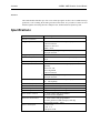
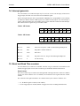
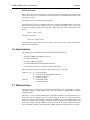
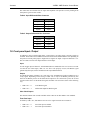
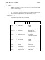
RCB 8047 CORBO
VME Read-Out Control Board
User's Manual, version 1.0
Designation: DOC 8047/UM
PN:
085.355
Version 1.0 - June 1995
Warranty Information
The information in this document has been checked carefully and is thought to be entirely reliable.
However, no responsibility is assumed in case of inaccuracies. Furthermore, CES reserves the
right to change any of the products described herein to improve reliability, function or design.
CES neither assumes any liability arising out of the application or use of any product or circuit
described herein nor conveys any licence under its patent rights or the rights of others.
WARNING
THIS EQUIPMENT GENERATES, USES AND CAN RADIATE RADIO FREQUENCY
ENERGY AND MAY CAUSE INTERFERENCE TO RADIO COMMUNICATIONS IF NOT
INSTALLED AND USED IN ACCORDANCE WITH THE INSTRUCTION MANUAL. IT HAS
BEEN TESTED AND FOUND TO COMPLY WITH THE LIMITS OF A CLASS A
COMPUTING DEVICE PURSUANT TO SUB-PART J OF PART 15 OF FCC RULES,
WHICH ARE DESIGNED TO PROVIDE REASONABLE PROTECTION AGAINST SUCH
INTERFERENCES
WHEN
OPERATED
IN
A
COMMERCIAL
ENVIRONMENT.
OPERATION OF THIS EQUIPMENT IN A RESIDENTIAL AREA IS LIKELY TO CAUSE
INTERFERENCE; IN WHICH CASE, THE USER AT HIS OWN EXPENSE WILL BE
REQUIRED TO TAKE WHATEVER MEASURES ARE NECESSARY TO CORRECT THE
INTERFERENCE.
©
Creative Electronic Systems SA - June 1995 - All Rights reserved
The reproduction of this material, in part or whole, is strictly prohibited. For copy information,
please contact:
Creative Electronic Systems,
70, Route du Pont-Butin
P.O. Box 107
CH-1213 PETIT-LANCY 1
SWITZERLAND
The information in this document is subject to change without notice. Creative Electronic
Systems assumes no responsibility for any error that may appear in this document.
CORBO VME Readout Control Board
Contents
Contents
Abstract
1
Specifications
1
1. General description
3
1.2. Description summary...............................................................................................3
1.3. VME interface.........................................................................................................6
1.4. Interrupt generator....................................................................................................7
1.5. Event and Dead Time counters....................................................................................7
1.6. Input selection........................................................................................................8
1.7. Differential bus.......................................................................................................8
1.8. Front panel Input / Output........................................................................................9
1.9. BUSY mode.........................................................................................................10
1.10. CSRi Format......................................................................................................10
2. User's guide
11
2.1. Installation procedure..............................................................................................11
2.2. View of the board..................................................................................................12
2.3. Connectors...........................................................................................................13
2.4. How to set the base address......................................................................................13
2.5. How to select the Input / Output levels......................................................................14
2.6. How to change the Slow Clock period.......................................................................14
2.7. How to use several CORBOs...................................................................................14
2.8. Front Panel Display...............................................................................................16
2.9. Examples of use....................................................................................................16
2.10. Some simple problems.........................................................................................18
3. Software
3.1.
3.2.
3.3.
3.4.
19
Introduction..........................................................................................................19
Software availability..............................................................................................19
Where are these programs........................................................................................19
How to run the programs........................................................................................20
Annex - VME Connector
21
Contents
CORBO VME Readout Control Board
Abstract
This VME module handles up to four event interrupt signals. It takes care of VME interrupt
generation, event counting, Dead Time generation and control. It is possible to connect several
modules together when using them in a multiprocessor, multicrate data acquisition system.
Specifications
Standard
Number of Channels
Trigger Input
Double height VME module. A24 / D16
4
NIM or TTL selectable with front panel jumpers
Lemo 00 connector
Sensitive to low level
Width > 20 ns.
or Differential input (neg. = 2V, pos = 3V)
3M 8-pin connector
Trigger Input impedance
50 Ω ±1%
Fast Clear Input
NIM or TTL selectable with front panel jumper. Width >
50 ns
Fast Clear Input impedance
50 Ω ±1%
Busy output level
NIM or TTL selectable with front panel jumper. 50 Ω load
capability
Actice Low TTL
Active High NIM
Lemo 00 connector
or Differential output (neg. = 2V, pos = 3V)
3M 8-pin connector
Slow clock output level
NIM or TTL selectable with front panel jumper.
50 Ω load capability
Slow clock frequency
10 KHz
VME base address
selectable with four rotary switches
VME interrupt levels
programmable by use of VME registers
VME interrupt vectors
programmable by use of VME registers
Event number counters
4 x 32-bit counters fully programmable
External Fast clear capability
Dead time measurement
4 x 16-bit counters fully programmable
Overflow generates a VME interrupt (watch dog)
Measurement accuracy: 100 µs
Power consumption
0.1 A at -12 V
5 A at +5 V
Total power 25 W
CORBO VME Readout Control Board
Contents
1. General description
1.1. Introduction
The aim of this chapter is to give a good understanding of the module and of its properties. A
description of the operations the user has to do for proper use are given in the following chapter
(User's Guide).
Most data acquisition systems are now based on VME bus architecture's, with either one or more
processors scattered in different crates. We often face the problem of trigger distribution and ReadOut Dead Time control.
This module aims at addressing this problem and has been designed to be used in the new
multiprocessor acquisition system of the Omega spectrometer.
1.2. Description summary
This module houses four identical and independent channels. Each of them contains a TRIGGER
input, a BUSY output, two VME interrupt generators and two counters (one Event Counter used
to count the TRIGGER inputs and the other one used to measure the BUSY width Dead Time
Counter). The block diagram of one channel is shown in figure 1.
Although the module may be used in different ways, the main use (described on the flow chart of
figure 2) is the following:
•
when the TRIGGER input occurs, a BUSY signal is asserted, as well as a VME interrupt.
•
the Event Counter is incremented by one and the Dead Time Counter starts counting the Slow
Clock signal (100 µs period).
•
the BUSY signal will remain active until it is cleared by a VME access. As long as BUSY is
asserted, no other TRIGGER is accepted.
•
the content of the Dead Time Counter gives a measure of the BUSY active time.
•
if the BUSY remains active too long, a VME interrupt is sent.
Contents
CORBO VME Readout Control Board
One channel block diagram
Count Select
COUNTER
Trigger Select
M
U
X
Lemo TRIGGER In
Front Panel
Push Button
M
U
X
VME
IRQ_ACK
VME_IRQ
R
S
&
S
R
Differential Bus
TRIGGER In
CLEAR_BUSY
Lemo BUSY Out
COUNTER
EN
BUSY
VME
Differential Bus
BUSY out
100 µs Clk
Overflow
S
R
VME_IRQ
IRQ_ACK
Fig 1
The Trigger input may be the front panel (NIM or TTL) input, the front panel differential bus
input, the front panel push button or the signal generated by a software access to a special VME
register.
The event counter may count either the BUSY signal (in this case the event number is counted) or
the Trigger input (in this case the number of Triggers arriving during the Dead Time are counted).
The counter may be read and write through VME. It can be cleared by an external front panel signal
(Fast Clear).
The Dead Time Counter may be read and written through VME access. The written value is the
Time-Out value of the BUSY signal. The read value gives the duration of the BUSY signal. With
a Slow Clock running at 10 KHz, the maximum value is roughly 6.5 s.
CORBO VME Readout Control Board
Contents
State Diagram
IDLE
TRIG_INPUT
Y
Assert it
Assert Busy
Increment Event Counter
Sart Busy_Watchdog
IT_ACK
N
IT_ACK
N
ASSERT_IT
Y
CLEAR_BUSY
Wait For
Clear_Busy
Or Watchdog
WATCHDOG
Fig 2
In the following sections, will be given a description of the different parts of this module:
•
VME interface and address mapping
•
Interrupt generator
•
Counters
•
Input selection
•
Differential bus
•
Front panel Input / Output
•
CSR description
•
Front panel display
Contents
CORBO VME Readout Control Board
1.3. VME interface
The module has a VME slave interface A24 - D16, is a VME interrupter D08 (0) - I (7-1) and uses
256 bytes in the VME address field. Table 1 gives the mapping of the address space.
Table 1. Address mapping
Offset to
base
0x00
Name
Size
Function
CSR1
Word
CSR of channel 1
0x02
CSR2
Word
CSR of channel 2
0x04
CSR3
Word
CSR of channel 3
0x06
CSR4
Word
CSR of channel 4
0x10
Event Number1
Long Word
Event counter of channel 1
0x14
Event Number2
Long Word
Event counter of channel 2
0x18
Event Number3
Long Word
Event counter of channel 3
0x1C
Event Number4
Long Word
Event counter of channel 4
0x20
DeadTime1
Word
Dead Time counter of channel 1
0x22
DeadTime2
Word
Dead Time counter of channel 2
0x24
DeadTime3
Word
Dead Time counter of channel 3
0x26
DeadTime4
Word
Dead Time counter of channel 4
0x31
BIM1 CR0
Byte
Control of channel 1 event interrupt
0x33
BIM1 CR1
Byte
Control of channel 2 event interrupt
0x35
BIM1 CR2
Byte
Control of channel 3 event interrupt
0x37
BIM1 CR3
Byte
Control of channel 4 event interrupt
0x39
BIM1 VR0
Byte
Vector of channel 1 event interrupt
0x3B
BIM1 VR1
Byte
Vector of channel 2 event interrupt
0x3D
BIM1 VR2
Byte
Vector of channel 3 event interrupt
0x3F
BIM1 VR3
Byte
Vector of channel 4 event interrupt
0x41
BIM2 CR0
Byte
Control of channel 1 Time-Out interrupt
0x43
BIM2 CR1
Byte
Control of channel 2 Time-Out interrupt
0x45
BIM2 CR2
Byte
Control of channel 3 Time-Out interrupt
0x47
BIM2 CR3
Byte
Control of channel 4 Time-Out interrupt
0x49
BIM2 VR0
Byte
Vector of channel 1 Time-Out interrupt
0x4B
BIM2 VR1
Byte
Vector of channel 2 Time-Out interrupt
0x4D
BIM2 VR2
Byte
Vector of channel 3 Time-Out interrupt
0x4F
BIM2 VR3
Byte
Vector of channel 4 Time-Out interrupt
0x50
TEST1
Word
Simulate input trigger 1
0x52
TEST2
Word
Simulate input trigger 2
0x54
TEST3
Word
Simulate input trigger 3
0x56
TEST4
Word
Simulate input trigger 4
0x58
CLEAR1
Word
Clear BUSY channel 1
0x5A
CLEAR2
Word
Clear BUSY channel 2
0x5C
CLEAR3
Word
Clear BUSY channel 3
0x5E
CLEAR4
Word
Clear BUSY channel 4
CORBO VME Readout Control Board
0x60 to 0xFE
RAM
Contents
Word
Static memory
Contents
CORBO VME Readout Control Board
1.4. Interrupt generator
For each channel, two VME interrupts may be used: one is the event interrupt (related to the
Trigger input), the other one is the Time-Out on the BUSY signal.
Each of the eight interrupts, has a programmable VME IRQ level, programmable vector and may
be enabled or disabled. Sixteen VME registers are available for this purpose. For each interrupt, a
register called VRi defines the vector number and a register called CRi controls the VME interrupt.
The contents of these registers are given in table 2 and 3.
Table 2. VRi format
D07
D06
D05
D04
D03
D02
D01
D00
D7
D6
D5
D4
D3
D2
D1
D0
D07
D06
D05
D04
D03
D02
D01
D00
L2
L1
L0
Table 3. CRi format
F
FAC X/IN
IRE IRAC
Bit <02...00>
L2, L1, L0
VME Interrupt Level
Bit <03>
IRAC
Auto-Clear. If equal to 1, IRE is cleared during the IRQ ACK
Bit <04>
IRE
IRQ enable / disable. Enable if 1
Bit <05>
X/IN
Has to be 0
Bit <06>
FAC
Flag Auto Clear. If 1, Flag is cleared during the IRQ ACK
Bit <07>
F
Test & Set Flag
1.5. Event and Dead Time counters
For each channel, two counters are available. The first one gives either the event number or the
number of trigger inputs received. The second one gives the BUSY duration measurement.
Event Counter
This 32 bit counter may be read and write through VME. The high order bits of data are at address
2n; the low order at address 2n+2. If enabled, an external Fast Clear signal clears the counter
contents.
The selection of the signal which has to be counted is done by the content of CSR bit <05>:
•
if 1, the BUSY signal is counted (event number)
•
if 0, the Trigger input is counted (number of triggers received even during the Dead Time)
CORBO VME Readout Control Board
Contents
Dead Time Counter
This 16-bit counter, counts the number of Slow Clock which occurred during the duration of the
BUSY signal. This gives a measurement of the BUSY signal (i.e the Read-Out Dead Time) with
an accuracy of 100 µs.
This counter may be read and written through VME.
When the counter overflows, a VME interrupt is sent (if enabled in the BIM2). If the counter starts
at 0, then the overflow occurs roughly 6.5 s later. To avoid such a long Time-Out, it is possible
to start the counting at an offset value defined by a VME write to the counter. Then the Time-Out
will be:
(65536 - offset) * 100 µs
The BUSY time will be:
(value read - offset) * 100 µs
The initialization of the counter has just to be done once. Then the offset value is automatically
loaded at the start of BUSY.
1.6. Input selection
The Trigger input of each channel may be chosen between different sources:
•
front panel LEMO input (NIM or TTL level)
•
front panel push button
•
front panel input differential bus
•
inverted and filtered front panel input differential bus
•
internal pulse generated by a VME write at the TESTi register
The selection between these possibilities is done with three bits in the CSRi:
CSRi <03...02> 00
01
10
11
CSR <07>
0
1
= Front panel input
= Filtered and inverted differential input bus
= Differential input bus
= Internal test input
= Push button enable
= Push button disable
1.7. Differential bus
Two differential bus connectors are available on the front panel. One, called INPUT, is used to
transmit the Trigger to several board in an easy way. The second one, called OUTPUT, transmits
the BUSY output.
The drivers / receivers used are AMD26LS38, which allow transmission on long distances (up to
50 m) and wired OR capability. This is very useful for the BUSY line: if we have more than one
VME crate involved in the Read-Out, we need one CORBO per crate. The total Dead Time is the
longest one. Thanks to the wired OR of the BUSY signals, the BUSY on the differential bus will
be present as long as one of the CORBO's drives BUSY. The BUSY signal on the differential bus
may be available as a NIM or TTL signal on the LEMO output of the front panel (see next topic).
Contents
CORBO VME Readout Control Board
The connectors used for these bus are 8-pin 3M compatible. The pin out as seen by looking at the
front panel is given in table 4 and 5.
Table 4. Input Differential Bus Connector
Left
Right
Input1>
Input1<
Input2>
Input2<
Input3>
Input3<
Input4>
Input4<
Table 5. Output Differential Bus Connector
Left
Right
Ouput1>
Ouput1<
Ouput2>
Ouput2<
Ouput3>
Ouput3<
Ouput4>
Ouput4<
1.8. Front panel Input / Output
In addition to the two differential Input / Output buses, ten others Input / Output signals are
available. Each of them uses LEMO 00 connector and electrical standard NIM or TTL depending on
the position of front panel jumpers. Eight of these signals are Input / Output of channels 1 to 4.
The two others are Fast Clear input and Slow Clock output.
Input
It is the Trigger input of channel i. In both NIM and TTL standard the low level is active. In order
to select the use of this input, CSRi <03...02> have to be properly set (00). The BUSY signal
generated by this input, will be forwarded on the output differential bus.
Output
It is the BUSY output of channel i. It is TTL active low, and NIM active high (in NIM it acts as a
ready signal). Depending on the setting of CSRi <04> it may be the BUSY generated by this
board or the BUSY present on the differential output bus. In a multicrate system, the second
selection makes the or of all the BUSY signals available. The selection is done in the following
way:
•
CSRi <04> = 0
Local BUSY signal
•
CSRi <04> = 1
Differential output bus BUSY signal
Slow Clock Output
The internal 10 KHz clock is made available on this connector in either NIM or TTL standard.
Fast Clear Input
If enable by CSRi <06>, this NIM or TTL active low signal clears the Event counter i.
•
CSRi <06> = 0
Fast Clear input is enabled
•
CSRi <06> = 1
Fast Clear input is disabled
CORBO VME Readout Control Board
Contents
1.9. BUSY mode
The BUSY may be either a level set by the input and reset by a VME write to the CLEAR
register, or a fan out of the input.
CSRi <01> selects one of these two modes of operation.
In both case a VME interrupt may be sent but in the second mode, the Dead Time control is very
poor : as soon as a VME interrupt is acknowledged, a new one will appear when a new input
signal arrives. Nevertheless this mode may be useful to distribute signals (see § 2.6).
1.10. CSRi Format
For each channel a CSR is available. Table 6 gives its format.
After a VME SYSRESET, the CSRi <00...07> bits are set to one. This means in particular that
all the channels are disabled.
D11
D10
D09
D08
D07
D06
D05
D04
D03
D02
D01
D00
R
R
R
R
R/W
R/W
R/W
R/W
R/W
R/W
R/W
R/W
Bit <00>
R/W
Channel enable
0 Enable
1 Disable
Bit <01>
R/W
BUSY mode
0 BUSY is a level set by the input
1 BUSY follows the input
Bit <02...03>
R/W
Input selection
Bit <04>
R/W
BUSY output selection
0 Local BUSY
1 Differential output BUSY
Bit <05>
R/W
Counter selection
0 Count input
1 Count BUSY
Bit <06>
R/W
Fast Clear enable
0 Enable
1 Disable
Bit <07>
R/W
Push button enable
0 Push button enable
1 Push button resets the VME IRQ
Bit <08>
R
Input state
10 Input present
Bit <09>
R
Local BUSY state
10 local BUSY present
Bit <10>
R
Differential output BUSY state 10 Differential output BUSY present
Bit <11>
R
VME interrupt state
00
01
10
11
Front panel input
Differential input bus
Differential output bus
Internal test pulse
0 IRQ pending
CORBO VME Readout Control Board
2. User's Guide
2. User's guide
Warnings
1. Please make sure that the power of the VME crate is off before inserting the board.
2. Some components are sensitive to static discharges. To avoid damage, minimise handling.
Precautions against static discharges must be taken.
2.1. Installation procedure
Before inserting the board in a VME crate, the following has to be done:
❶ Set the base address of the board (see § 2.4)
❷ Select the proper level for Input / Output (see § 2.5)
❸ Switch the VME power off
❹ If between the slot which will be occupied by the module and the CPU which will receive the
interrupt, there are empty slots, jumpers have to be installed on the IACKIN IACKOUT daisy
chain of the empty slots
❺ Insert the board
❻ Power the crate on
❼ Send SYSRESET (if there is not one at the power on)
2. User's Guide
CORBO VME Readout Control Board
2.2. View of the board
A view of the board, with the location of the different parts the user may have to change is given
in figure 3.
View of the board
PUSH BUTTON
C
L
O
C
K
SLOW CLOCK
OSCILLATOR
V
M
E
I
N
1
B
U
S
Y
I
N
2
B
U
S
Y
A23
A20
A19
A16
A15
A12
A11
A08
ROTARY SWITCHES
FOR
BASE ADDRESS
I
N
3
B
U
S
Y
I
N
4
B
U
S
Y
I
N
P
U
T
C
L
E
A
R
Fig 3
O
U
T
P
U
T
D
I
F
F
E
R
E
N
T
I
A
L
TERMINATION
RESISTORS
OF
DIFFERENTIAL
BUS
C
O
N
N
E
C
T
O
R
CORBO VME Readout Control Board
2. User's Guide
Front panel display
Twelve LEDs give the display of one of the CSRi. A front panel switch allows to select the CSRi
which has to be displayed.
2.3. Connectors
Differential Input
It receives 3M 8-pin connector for 4 pairs flat cable. The pin out as view from the front panel is:
Left
Right
Input1>
Input1<
Input2>
Input2<
Input3>
Input3<
Input4>
Input4<
Differential BUSY
It receives 3M 8-pin connector for 4 pairs flat cable. The pin out as view from the front panel is:
Left
Right
Output1>
Output1<
Output2>
Output2<
Output3>
Output3<
Output4>
Output4<
2.4. How to set the base address
In the VME A24 address field, the board responds to the following addresses:
A23
..
A8
x
x
x
x
x
x
x
x
The base address of the board is defined by bits <23...08>. Four rotary switches are available on
the board to define them. Figure 4 gives the link between the rotary switches and the address.
Rotary switches view from top
Fig 4
A23
A20
A19
A16
A15
A12
A11
A08
Rotary Switches
For
Base Address
2. User's Guide
CORBO VME Readout Control Board
2.5. How to select the Input / Output levels
Each signal on the LEMO 00 connectors may be defined as NIM or TTL level. To do the
selection, a jumper is available close to each connector. The level selection is done as shown in
figure 5.
NIM/TTL selection
N
Fig 5
2.6. How to change the Slow Clock period
It may happen that the Slow Clock frequency is not adapted to the application. To change it,
replace the Slow Clock oscillator (shown in figure 3) by another one.
2.7. How to use several CORBOs
There are different ways of connecting the modules together.
❶ One can connect all the differential BUSY output together with a four twisted pair flat cable
equipped with female 3M 8-pin connectors and distribute the Trigger as a coaxial NIM or TTL
signal to all the boards on the same channel number.
One of the CORBOs has to be initialized so that its coaxial NIM or TTL output is reflecting
the BUSY on the differential bus. Due to the wired or, this will be the total BUSY of the
system and it can be used as a veto for the Trigger source.
Only the first and the last modules on the chain must have the termination resistors (shown
on figure 3). These resistors networks must be removed on the intermediate modules.
❷ One can do the same thing but uses a differential driver to distribute the Trigger. In this case,
one has to connect all the differential Trigger input together with a four twisted pair flat cable
equipped with female 3M 8-pin connectors One possible driver is the MODEL V64 from
CAEN, used in TTL mode.
❸ One can use a single flat cable to connect together all the differential Trigger inputs and
differential BUSY outputs (as shown on figure 6). Only the last CORBO needs termination
resistors. All the others must be removed.
One of the CORBO receives the Trigger on coaxial input1 and is initialized so that BUSY is
not latched. The Trigger is also sent on coaxial input2 initialized in a normal way. All the
others CORBOs use also channels 1 and 2 in the following way:
- channel 1 is initialized to receive Trigger from differential input 1 and to have an unlatched
BUSY (CSR<1> = 1). The coaxial BUSY output is connected to coaxial Trigger input 2.
- channel 2 is initialized to receive Trigger from coaxial input.
CORBO VME Readout Control Board
2. User's Guide
Connection of several CORBOs
Trigger
Input
VETO
Trigger
Input
1
2
In
Busy
In
Busy
Differential
INPUT
Trigger
Input
1
2
In
Busy
In
Busy
Differential
INPUT
1
2
OUTPUT
OUTPUT
OUTPUT
In
Busy
In
Busy
Differential
INPUT
SOLUTION 1
1
VETO
2
In
Busy
In
Busy
Differential
INPUT
1
2
2
In
Busy
In
Busy
Differential
INPUT
OUTPUT
SOLUTION 2
Trigger
Input
1
VETO
2
In
Busy
In
Busy
Differential
INPUT
OUTPUT
1
2
In
Busy
In
Busy
Differential
INPUT
OUTPUT
SOLUTION 3
Fig 6
1
OUTPUT
OUTPUT
DIFFERENTIAL
DRIVER
In
Busy
In
Busy
Differential
INPUT
1
2
In
Busy
In
Busy
Differential
INPUT
OUTPUT
2. User's Guide
CORBO VME Readout Control Board
2.8. Front Panel Display
The content of CSRi may be displayed on front panel LEDs. The meaning of this display is given
in table 7 (from the top to the bottom).
Table 7. Front panel display
Front panel
name
CSR bit
ON meaning
In reflect
CSR <08>
Input signal is present
Busy
CSR <09>
Local BUSY is set
Ext. Busy
CSR <10>
Differential bus output BUSY is set
BIM-Int
CSR <11>
VME IRQ is set
EN.I/P
CSR <00>
Channel is enabled
Free
CSR <01>
BUSY output is equal to the Input
Sel.1
CSR <02>
Bit is set
Sel.2
CSR <03>
Bit is set
Busy-Sel.
CSR <04>
Output is Local BUSY
Cnt-Sel.
CSR <05>
Counter counts Input
En.Ext-Clr
CSR <06>
Fast Clear is enabled
En.Test
CSR <07>
Push button is enabled
To select the CSR number to be displayed, two switches are available under the display. The
relationship between the switches position and the displayed CSR is given in table 8.
Table 8. Display selection
Top switch
Bottom
switch
CSRi
Right
Right
CSR1
Left
Right
CSR2
Right
Left
CSR3
Left
Left
CSR4
2.9. Examples of use
Two examples of initialization are given. The first one shows how to use the CORBO as a pulse
generator. The second one shows how to initialize the CORBO as Read-Out controller in a VME
Read-Out system
Pulse Generator
It is wanted to use the CORBO channel 1 as a NIM pulse generator controlled by a VME CPU.
Before inserting the board in the crate, one has to set the base address of the board (see § 2.3) The
BUSY output of channel 1 has to be selected as a NIM output (see § 2.4)
The channel 1 has to be initialized by written 0xEC in CSR1 (channel enabled, BUSY latched,
Internal test pulse as input).
To set the output a VME write cycle at TEST1 address has to be done (Busy will go to 0 V). To
reset it a VME write access at CLEAR1 address has to be done (Busy will go to 800 mV).
The minimum width of the pulse, is the minimum time between two consecutive VME access.
CORBO VME Readout Control Board
The content of EVENT NUMBER1 gives the number of pulses which were sent.
2. User's Guide
2. User's Guide
CORBO VME Readout Control Board
Read Out Controller
It is wanted to use the CORBO channel 1 as Read-Out trigger input. This signal comes from NIM
logic which has to be disabled during the Read-Out Dead Time. The maximum Read-Out Dead
Time is 3 m/s.
Before inserting the board in the VME crate, one has to set the base address properly (see § 2.3).
The INPUT1 and BUSY1 have to be selected as NIM signals (see § 2.4).
If there are missing boards between the CORBO and the CPU which will receive the interrupt, one
has to put jumpers on the IACK IN / OUT strap of the empty slots.
The NIM logic TRIGGER signal has to be connected to the INPUT 1. The BUSY1 signal has to
be put in coincidence with the NIM trigger logic so that the trigger is not sent during Dead Time.
Three tasks have to be written:
❶ Initialization
❷ Event Read-Out which will be started by the event interrupt
❸ BUSY Time-Out task which will be started if the BUSY signal exceeds 10 ms.
The Initialization Task is the following:
•
Write 0xEC in CSR1
•
Write in TEST1 to assert BUSY and so disable the external trigger generation
•
Write vector number of the event task in BIM1 VR0
•
Write vector number of the BUSY Time-Out task in BIM2 VR0
•
Clear Event Number1
•
Write 65536 - 100 = 65436 in Deadtime1 (to set the Time-Out at 10 ms)
•
Write #$ D0 in CSR1
•
Write 0 in CLEAR1 to release BUSY and allow the Trigger to be generated
•
Write BIM1 CR0 and BIM2 CR0 with the following byte:
0
0
0
1
0
L2
L1
L0
where <L2, L1, L0> is the VME IRQ level selected.
The Event Task is the following:
•
Read Event number1 to know the event number
•
Perform the Read-Out
•
Read the DeadTime1. The BUSY time was (65536 - read value) * 0.1 ms
•
Write 0 to CLEAR1 to release BUSY
The BUSY Time-Out Task is waked up by a VME interrupt. What it does depends of the
application.
CORBO VME Readout Control Board
2.10. Some simple problems
Here are given a few simple problems diagnostics.
VME Bus Error
Check the base address.
Interrupt Acknowledge Time-Out
Check the VME interrupt acknowledge daisy chain (IACKIN- IACKOUT)
2. User's Guide
CORBO VME Readout Control Board
3. Software Description
3. Software
Software has been developed by CES while testing the CORBO module for integration in a data
acquisition system. It consists of a low level library and a few test programs, all written in C. The
software is running under OS-9 but can fairly easily be ported to other environments. Please
contact CES for more information.
The description of the libraries given in § 3.1, § 3.2, § 3.3 and § 3.4 is specific and must be
ignored.
CORBO VME Readout Control Board
Annex - VME Connector
Annex - VME Connector
This 96-pin connector follows the VME specification. The pin assignment is given in the
following table.
Pin Number
Row A
Row B
Row C
1
D00
BBSY*
D08
2
D01
BCLR*
D09
3
D02
ACFAIL*
D10
4
D03
BG0IN*
D11
5
D04
BG0OUT*
D12
6
D05
BG1IN*
D13
7
D06
BG1OUT*
D14
8
D07
BG2IN*
D15
9
GND
BG2OUT*
GND
10
SYSCLK
BG3IN*
SYSFAIL*
11
GND
BG30UT*
BERR*
12
DS1*
BR0*
SYSRESET*
13
DS0*
BR1*
LWORD*
14
WRITE*
BR2*
AM5
15
GND
BR3*
A23
16
DTACK*
AM0
A22
17
GND
AM1
A21
18
AS*
AM2
A20
19
GND
AM3
A19
20
IACK*
GND
A18
21
IACKIN*
SERCLK
A17
22
IACKOUT*
SERDAT*
A16
23
AM4
GND
A15
24
A07
IRQ7*
A14
25
A06
IRQ6*
A13
26
A05
IRQ5*
A12
27
A04
IRQ4*
A11
28
A03
IRQ3*
A10
29
A02
IRQ2*
A09
30
A01
IRQ1*
A08
31
-12 V
+5 V STDBY
+12 V
32
+5 V
+5 V
+5 V