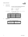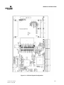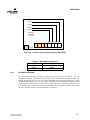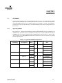
1
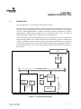
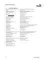
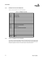
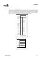
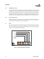
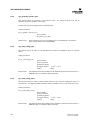
COMPACT PCI-821 SYSTEM CONTROLLER USER’S MANUAL The information in this document has been carefully checked and is believed to be entirely reliable. However, no responsibility is assumed for inaccuracies. Furthermore, Cyclone Microsystems, Inc. reserves the right to make changes to any products herein to improve reliability, function, or design. Cyclone Microsystems, Inc. neither assumes any liability arising out of the application or use of any product or circuit described herein, nor does it convey any license under its right or the rights of others. Revision 1.0, May 2003 Cyclone P/N 800-0821 Copyright 2003 by Cyclone Microsystems, Inc. CHAPTER 1 1.1 INTRODUCTION .................................................................................................................................1-1 1.2 FEATURES .........................................................................................................................................1-2 1.3 OVERVIEW .........................................................................................................................................1-2 1.4 SOFTWARE OVERVIEW....................................................................................................................1-3 1.5 SPECIFICATIONS...............................................................................................................................1-4 1.6 ENVIRONMENTAL..............................................................................................................................1-4 1.7 REFERENCE MANUALS ....................................................................................................................1-6 CHAPTER 2 2.1 PPC440GP PROCESSOR ..................................................................................................................2-1 2.2 BYTE ORDERING...............................................................................................................................2-1 2.3 ADDRESS MAP AND RESET VECTOR.............................................................................................2-1 2.4 PPC440GP CORE CACHE MEMORIES ............................................................................................2-1 2.5 MEMORY MAP....................................................................................................................................2-2 2.6 INTERRUPTS......................................................................................................................................2-2 2.6.1 External Interrupts ......................................................................................................................2-3 2.6.2 INTERRUPT VECTOR OFFSET REGISTERS ..........................................................................2-4 2.6.3 LOCAL PCI INTERRUPT STATUS REGISTER .........................................................................2-4 2.6.4 INTERRUPT MASKING..............................................................................................................2-5 CHAPTER 3 3.1 DDR SDRAM.......................................................................................................................................3-1 3.1.1 Upgrading SDRAM .....................................................................................................................3-1 3.1.2 SDRAM Configurations Installation and Removal of Memory Modules......................................3-2 3.2 FLASH ROM........................................................................................................................................3-2 3.2.1 Non-Volatile Parameter Memory.................................................................................................3-3 3.3 CONSOLE SERIAL PORT ..................................................................................................................3-4 3.4 JTAG EMULATOR SUPPORT ............................................................................................................3-4 3.5 COUNTER/TIMERS ............................................................................................................................3-5 3.5.1 PPC440GP Core Timers.............................................................................................................3-6 3.5.2 General Purpose Timers.............................................................................................................3-6 3.6 LEDS ...................................................................................................................................................3-6 3.6.1 User LEDs During Initialization ...................................................................................................3-7 3.7 PCI INTERFACE .................................................................................................................................3-7 3.8 GEOGRAPHIC ADDRESSING ...........................................................................................................3-8 3.9 POWER SUPPLY MONITORING .......................................................................................................3-8 3.10 FAN MONITORING ...........................................................................................................................3-9 3.11 I2C BUS.............................................................................................................................................3-9 3.11.1 SDRAM EEPROM ..................................................................................................................3-10 3.11.2 Temperature Sensors .............................................................................................................3-10 3.11.3 Serial EEPROM ......................................................................................................................3-10 3.11.4 Phase Lock Loop Clock Driver................................................................................................3-10 3.12 ETHERNET PORTS........................................................................................................................3-11 CPCI-821 User’s Manual Revision 1.0, May 2003 i 3.12.1 Ethernet Port LEDs.................................................................................................................3-11 3.12.2 Ethernet Port Connector .........................................................................................................3-11 CHAPTER 4 4.1 INTRODUCTION .................................................................................................................................4-1 4.2 BREEZE DEVELOPMENT ENVIRONMENT™ FEATURES..............................................................4-1 4.3 INITIALIZATION OF THE CPCI-821 ...................................................................................................4-1 4.4 DOWNLOADING CODE......................................................................................................................4-2 4.5 FLASH ROM PROGRAMMING...........................................................................................................4-2 4.6 PCI BIOS ROUTINES .........................................................................................................................4-2 4.6.1 sys_pci_bios_present .................................................................................................................4-2 4.6.2 sys_find_pci_device....................................................................................................................4-3 4.6.3 sys_find_pci_class_code ............................................................................................................4-3 4.6.4 sys_generate_special_cycle .......................................................................................................4-4 4.6.5 sys_read_config_byte .................................................................................................................4-4 4.6.6 sys_read_config_word ................................................................................................................4-4 4.6.7 sys_read_config_dword ..............................................................................................................4-5 4.6.8 sys_write_config_byte.................................................................................................................4-5 4.6.9 sys_write_config_word................................................................................................................4-5 4.6.10 sys_write_config_dword............................................................................................................4-6 4.6.11 sys_get_irq_routing_options .....................................................................................................4-6 4.6.12 sys_set_pci_irq .........................................................................................................................4-6 4.7 PRINT_PCI UTILITY ...........................................................................................................................4-6 4.8 PCI LIST UTILITY................................................................................................................................4-7 4.9 CPCI-821 DIAGNOSTICS ...................................................................................................................4-7 ii CPCI-821 User’s Manual Revision 1.0, May 2003 CONTENTS LIST OF FIGURES Figure 1-1. CPCI-821 Block Diagram ....................................................................................................1-1 Figure 1-2. CPCI-821 Physical Configuration ........................................................................................1-5 Figure 2-1. CPCI-821 Breeze Memory Map .........................................................................................2-2 Figure 2-2. Local PCI Interrupt Status Register, E800 0002H ...............................................................2-5 Figure 3-1 Breeze Boot Block Map .......................................................................................................3-3 Figure 3-2. Breeze Block Structure........................................................................................................3-3 Figure 3-3. Boot Block Structure............................................................................................................3-4 Figure 3-4. LED Register Bitmap, E800 0001H .....................................................................................3-6 Figure 3-5. Geographic Addressing Register, E800 0001H.................................................................. 3-8 Figure 3-6. Power Supply Status Register, E800 0000H.......................................................................3-9 LIST OF TABLES Table 1-4. Table 1-2. Table 2-1. Table 2-2. Table 2-3. Table 3-1. Table 3-2. Table 3-3. Table 3-4. Table 3-5. Table 3-6. Table 3-7. CPCI-821 Power Requirements ..........................................................................................1-4 Environmental Specifications ..............................................................................................1-4 CPCI-821 EXTERNAL INTERRUPTS.................................................................................2-3 INTERRUPT VECTORS......................................................................................................2-4 PMC IDSEL Assignments....................................................................................................2-5 Supported SDRAM Configurations......................................................................................3-1 Console Serial Port Connector ............................................................................................3-4 JTAG Emulator Pin Assignment Wind River .......................................................................3-5 JTAG Emulator Pin Assignment IBM...................................................................................3-5 BREEZE START-UP LEDS.................................................................................................3-7 I2C Device Addresses .......................................................................................................3-10 100BaseTx Connector.......................................................................................................3-11 CPCI-821 User’s Manual Revision 1.0, May 2003 iii CHAPTER 1 GENERAL INTRODUCTION 1.1 INTRODUCTION The CompactPCI-821 is a CompactPCI Hot Swap host controller. The board is based on the IBM PowerPC 440GP microprocessor. The PPC440GP processor incorporates a superscalar implementation of the Book-E enhanced PowerPC architecture, a PCI-X bridge controller, a DDR SDRAM Memory Controller, External Bus Controller (flash interface), Memory Management Unit (MMU), DMA Controllers (4), two 10/100BaseTx Ethernet ports, two universal interrupt controllers, a UART, an I2C controller and a general purpose timer. Software development tools for the PPC440GP processor are available from a variety of vendors. Board Support Packages (BSPs) for the VxWorks and pSOS real-time operating systems are available from Cyclone. In addition, Cyclone provides the Breeze Development Environment to support the development of software for the CPCI-821. Breeze handles the initialization of the adapter board after a reset, and supplies the user with a set of example utilities designed to speed software development on the CPCI-821. Compact PCI System Board 64 bits Intel 21154BC Local PCI bus 3.3V Ethernet Controller Intel 82559ER Ethernet Controller Intel 82559ER IBM PPC 440 400MHz JTAG I/F PMC 60 512 or 256 Mbytes DDR SDRAM PC266 Console Serial Port Flash ROM Figure 1-1. CPCI-821 Block Diagram CPCI-821 User’s Manual Revision 1.0, May 2003 1-1 GENERAL INTRODUCTION 1.2 1.3 • FEATURES PPC440GP Processor • Intel 21154BC The 21154 has a 64-bit primary bus interface and a 64-bit secondary interface. The 21154 secondary bus interfaces with the 64-bit CompactPCI bus and the primary bus interfaces with the 64-bit local PCI bus and the IBM PPC440GP and PMC module. This allows the CPCI-821 to function as a system controller in a CompactPCI system. • SDRAM 256 to 512 MBytes of DDR SDRAM via a 200 pin SoDIMM. • PMC Module The CPCI-821 has one location for 64-bit PMC PCI Modules. The module can contain I/O interfaces to customize the CPCI-821 for different applications. On the CPCI-821, this location is populated with a Cyclone PMC60 dual Ethernet module (see Ethernet ports below) • CompactPCI Interface The CPCI-821 meets the PICMG 2.0 Rev. 3.0 and ECR 001 Specification for host slot adapters. • Console Serial Port An RS-232 serial port is provided for a console terminal or workstation connection. It supports up to 115 Kbps and uses a phone jack to DB25 cable supplied with the CPCI-821 board. • Timers The PPC440GP contains one 64-bit time base, one 32-bit decrementer, one fixed timer and one watchdog timer. • Flash ROM 8 Mbytes of in-circuit sector-programmable Flash ROM provides non-volatile storage on the CPCI-821. One 128 Kbyte sector of the Flash ROM is reserved for the storage of non-volatile boot and system parameters. Flash device is a 28F640J3A-120 • DMA Controller The PPC440CP supports 4 separate DMA channels for high throughput data transfers between PCI bus agents and the local SDRAM memory. • Ethernet Ports Two 10/100BaseTx Ethernet ports are provided. Each port supports up to 100Mbps a uses a RJ45 style module phone jack. The interfaces are contained within a permanently mounted PMC60 and are based upon Intel’s 82559ER Fast Ethernet controller. The microprocessor is IBM’s 32-bit reduced instruction set computer (RISC) embedded processor. The device is a system-on-a-chip design that integrates a PowerPC embedded processor core running at 400 MHz with a mix of peripheral cores by implementing IBM’s high speed CoreConnect technology. The core boasts a 32 Kbyte instruction cache and a 32 Kbyte data cache. The PCI bridge provides the connection path to a 64-bit PCI bus. Memory can be accessed through the memory controller from the core processor or the PCI bus. OVERVIEW The CPCI-821 is 6U double height CompactPCI host card with support for one PMC Module. The board features a 400 MHz IBM PPC440GP embedded processor. 1-2 CPCI-821 User’s Manual Revision 1.0, May 2003 GENERAL INTRODUCTION The IBM PPC440GP 32-bit reduced instructions set computer (RISC) embedded processor is a systemon-a-chip (SOC) design that integrates a PowerPC 440 embedded processor core with a mix of peripheral cores. It features a 400 MHz core that is a superscalar implementation of the Book-E Enhanced PowerPC Architecture. The IBM PPC440GP is a multifunction device that integrates the processor core with a 64-bit PCI bus, a Memory Controller, a DMA Controller, an I2C Bus Interface Unit, two Ethernet ports, a UART, and other specific features into a single system. This multifunction PCI device is fully compliant with the PCI Local Bus Specification, Revision 2.2 and PCI-X Addendum to the PCI Local Bus Specification, Version 1.0 compliant. Note that on the CPCI-821 both PCI busses are limited to 33 MHz operation The 21154BC secondary PCI bus is the interface to the CompactPCI backplane. The CPCI-821 is configured as a system host board. Therefore, the CPCI-821 provides the interrupt, arbitration, clocking and reset function for the other peripheral adapters in the CompactPCI system. The 21154BC primary PCI bus is the interface to the IBM PPC440GP and the PMC 60. The CPCI-821 adapter includes the Breeze Development Environment. Breeze handles initialization of the adapter hardware and provides a set of example utilities to speed application development. In production systems, this component remains in place, and transparently boots the user application. Automatic booting is available to standalone applications as well as those built on a real-time operating system such as VxWorks or pSOS. The Flash ROM on the CPCI-821 can be reprogrammed by software in 128 Kbyte blocks, a feature that allows Breeze to download applications directly into Flash ROM. Aside from eliminating the need to reprogram the entire Flash every time a small change is made to the downloaded code, this feature also allows Breeze itself to be placed in separate blocks in the Flash ROM, obviating the need for an additional boot PROM. The sectors occupied by Breeze cannot be erased with the included Flash ROM utilities, as this would render the system unbootable. Cyclone includes a CD with each CPCI-821 adapter. This CD contains example code and header files necessary for programming the CPCI-821. The CD also includes any changes to the printed documentation. 1.4 SOFTWARE OVERVIEW The Flash ROM on the CPCI-821 is factory-loaded with Cyclone’s Breeze firmware. Breeze is responsible for initializing board hardware and configuring the PCI subsystem. Breeze resides in the upper blocks of the Flash ROM. Users should be careful not to erase these blocks, as doing so will render the board unbootable. Breeze also provides a simple development environment for users that wish to develop software without using a real time operating system. Users can set up Breeze to autoboot (automatically execute) their applications. For users that wish to use a real-time operating system, Cyclone offers Board Support Packages for several RTOSs, including VxWorks, pSOS, and Linux. These Board Support Packages execute on top of Breeze; Breeze performs most of the hardware initialization before passing control to the operating system via the autoboot procedure. CPCI-821 User’s Manual Revision 1.0, May 2003 1-3 GENERAL INTRODUCTION 1.5 SPECIFICATIONS Physical Characteristics The CPCI-821 is a single slot, double high CompactPCI card with a host slot interface. This product is equipped with an IBM PPC440GP microprocessor and a PMC 60 permanently installed. Height Double Eurocard Depth Width Power Requirements 9.187” (233.35mm) (6U) 6.299” (160mm) .8” (20.32mm) The CPCI-821 requires +5V, +12V, -12V and +3.3V from the CompactPCI backplane J1 connector. Table 1-1. CPCI-821 Power Requirements 1.6 Voltage Current Typical Current Maximum +3.3V 2.61 Amps 3.76 Amps +5V 0.14 Amps 0.20 Amps +12V 0.0 Amps 0.0 Amps -12V 0.0 Amps 0.0 Amps ENVIRONMENTAL A small amount of airflow is required, such as is found in a typical Eurocard enclosure. Table 1-2. Environmental Specifications Operating Temperatures 0 to 55 Degrees Celsius Relative Humidity (non-condensing) Storage Temperatures 1-4 0-95% -55 to 125 Degrees Celsius CPCI-821 User’s Manual Revision 1.0, May 2003 GENERAL INTRODUCTION Figure 1-2. CPCI-821 Physical Configuration CPCI-821 User’s Manual Revision 1.0, May 2003 1-5 GENERAL INTRODUCTION 1.7 REFERENCE MANUALS PPC440GP Embedded Processor User’s Manual IBM Microelectronics Division 1580 Route 52, Bldg. 504 Hopewell Junction, NY 12533-6531 http://www.chips.ibm.com CompactPCI Specification PICMG 2.0 R3.0 (Include ERC001) PCI Industrial Computers Manufacturing Group 401 Edgewater Place, Suite 500 Wakefield, MA 01880 (781) 224-1100 (781) 224-1239 Fax www.picmg.org 21154 PCI-to-PCI Bridge Order Number 278108-002 Intel Corporation Literature Sales P.O. Box 7641 Mt. Prospect, IL 60056-7641 (800) 879-4683 www.intel.com PCI Local Bus Specification, Revision 2.2 PCI Special Interest Group 5440 SW Westgate Dr. Suite #217 Portland, OR 97221 (800) 433-5177 (U.S.) (503) 222-6190 (International) (503) 222-6190 (Fax) [email protected] 82559ER Data Intel Corporation Literature Sales PO Box 7641 Mt. Prospect, IL 60056-7641 (800) 879-4683 www.intel.com CompactPCI Hot Swap Specification, PICMG 2.1, R2.0 PCI Industrial Computers Manufacturing Group 401 Edgewater Place, Suite 500 Wakefield, MA 01880 (781) 224-1100 (781) 224-1239 Fax www.picmg.org LM75 Digital Temperature Sensor and Thermal Watchdog National Semiconductor Corporation 1111 West Bardin Road Arlington, TX 76017 (800) 272-9959 http://www.national.com PMC on CompactPCI Specification, PICMG 2.3, R1.0 PCI Industrial Computers Manufacturing Group 401 Edgewater Place, Suite 500 Wakefield, MA 01880 (781) 224-1100 (781) 224-1239 Fax www.picmg.org PCI-X Addendum to the PCI Local Bus Specification, Revision 1.0 PCI Special Interest Group 5440 SW Westgate Dr. Suite #217 Portland, OR 97221 (800) 433-5177 (U.S.) (503) 222-6190 (International) (503) 222-6190 (Fax) [email protected] IEEE STD, P1386/Draft 2.2 345 East 47th Street New York, NY 10017-2394 1-6 CPCI-821 User’s Manual Revision 1.0, May 2003 CHAPTER 2 PROCESSOR 2.1 PPC440GP PROCESSOR The PPC440GP processor is a superscalar 32-bit implementation of the Book E Enhanced PowerPC® architecture. The core is configured to run at 400 MHz. The core features independently configurable instruction and data caches. Both the instruction and the data caches are 64-way 32 Kbytes. 2.2 BYTE ORDERING The CPCI-821 is configured to access external devices in big endian mode. The byte ordering determines which memory location stores the most significant byte of the operand. Big endian stores the most significant byte in the lowest address. 2.3 ADDRESS MAP AND RESET VECTOR As a 32-bit implementation of the Book-E Enhanced PowerPC Architecture, the PPC440GP implements a uniform 32-bit effective address space. Effective addresses are expanded into virtual addresses and then translated to 36-bit (64GB) real addresses by the memory management unit. The PPC440GP generates an effective address whenever it executes a storage access, branch, cache management, or translation lookaside buffer management instruction, or when it fetches the next sequential instruction. The 8-bit wide Flash ROM is located in the address range FF80 0000h through FFFF FFFFh. See Figure 2-1, the CPCI-821 memory map. The PPC440GP reset vector is located at address FFFF FFFCh. This reset vector location, which contains a branch to the rest of the boot code, is essentially at the end of the ROM device. 2.4 PPC440GP CORE CACHE MEMORIES The PPC440GP provides separate instruction and data cache controllers and arrays, which allow concurrent access and minimize pipeline stalls. The storage capacity of both cache arrays is 32 Kbytes. Both cache controllers have 32-byte lines, and both are highly associative, having 64-way set-associativity. The PowerPC instruction set provides a rich set of cache management instructions for softwareenforced coherency. The PPC440GP implementation also provides special debug instructions that can directly read the tag and data arrays. The cache controllers interface to the processor local bus for connection to the IBM CoreConnect system-on-a-chip environment. The instruction and data cache arrays are organized identically, although the fields of the tag and data portions of the arrays are slightly different because the functions of the arrays differ, and because the instruction cache is virtually tagged while the data cache has real tags. There are 64 ways in each set, with a set consisting of all 64 lines (one line from each way) at which a given memory location can reside. Conversely, there are 16 sets in each way, with a way consisting of 16 lines (one from each set). CPCI-821 User’s Manual Revision 1.0, May 2003 2-1 PROCESSOR 2.5 MEMORY MAP Figure 2-1 shows the CPCI-821 memory map as configured by Breeze Firmware. FFFF FFFFh FLASH ROM FF80 0000h UNUSED F000 0000h PERIPHERALS E000 0000h PCI I/O Local PCI Interrupts (Read Only) D000 0000h INTERNAL SRAM C000 0000h PCI Memory 8000 0000h UNUSED 6000 0000h DDR* SDRAM NON-CACHEABLE E800 0002h LED Register (Write Only) Geographic Address (Read Only) Power Supply Status (Read Only) E800 0001h E800 0001h E800 0000h 4000 0000h UNUSED 2000 0000h * These are physically the same locations DDR* SDRAM CACHEABLE 0000 0000h Figure 2-1. CPCI-821 Breeze Memory Map 2.6 INTERRUPTS An interrupt is the action in which the PPC440GP saves its old context (Machine State Register (MSR) and next instruction address) and begins execution at a pre-determined interrupt-handler address, with a modified MSR. Exceptions are the events that may cause the processor to take an interrupt, if the corresponding interrupt type is enabled. Exceptions may be generated by the execution of instructions, or by signs from devices external to the PPC440GP, the internal timer facilities, debug events, or error conditions. 2-2 CPCI-821 User’s Manual Revision 1.0, May 2003 PROCESSOR All interrupts, except for Machine Check, can be categorized according to two independent characteristics of the interrupt. They are asynchronous or synchronous and critical and non-critical. Asynchronous interrupts are caused by events that are independent of instruction execution. For asynchronous interrupts, the address reported to the interrupt handling routine is the address of the instruction that would have executed next, had the asynchronous interrupt not occurred. Synchronous interrupts are those that are caused directly by the execution (or attempted execution) of instructions. Critical interrupt and non-critical interrupts use different save/restore register pairs. Machine check interrupts are typically caused by some kind of hardware or storage subsystem failure, or by an attempt to access an invalid address. 2.6.1 External Interrupts On the CPCI-821 the external interrupts are connected to the PPC440GP as shown in Table 2-1. The local PCI interrupts are shared. Therefore, to determine which of the four local PCI interrupts caused the interrupt, a local board register is provided at address E800 0002h. Table 2-1. CPCI-821 EXTERNAL INTERRUPTS Interrupt Input Interrupt Type IRQ0 CPCI INTERRUPT A IRQ1 CPCI INTERRUPT B IRQ2 CPCI INTERRUPT C IRQ3 CPCI INTERRUPT D IRQ4 CPCI HOT SWAP ENUMERATION (ENUM#) IRQ5 NOT USED IRQ6 TEMPERATURE INTERRUPT IRQ7 FAN 0 INTERRUPT IRQ8 FAN 1 INTERRUPT IRQ9 POWER GOOD INTERRUPT IRQ10 LOCAL PCI BUS INTERRUPT CPCI-821 User’s Manual Revision 1.0, May 2003 2-3 PROCESSOR 2.6.2 INTERRUPT VECTOR OFFSET REGISTERS Table 2-2. shows the interrupt vector and the interrupt type. Table 2-2. INTERRUPT VECTORS IVOR 2.6.3 INTERRUPT TYPE IVOR0 CRITICAL INPUT IVOR1 MACHINE CHECK IVOR2 DATA STORAGE IVOR3 INSTRUCTION STORAGE IVOR4 EXTERNAL INPUT IVOR5 ALIGNMENT IVOR6 PROGRAM IVOR7 FLOATING POINT UNAVAILABLE IVOR8 SYSTEM CALL IVOR9 AUXILIARY PROCESSOR UNAVAILABLE IVOR10 DECREMENTER IVOR11 FIXED INTERVAL TIMER IVOR12 WATCHDOG TIMER IVOR13 DATA TLB ERROR IVOR14 INSTRUCTION TLB ERROR IVOR15 DEBUG LOCAL PCI INTERRUPT STATUS REGISTER The Local PCI interrupts LINTA# through LINTD# from the PMC module are logically OR’d together and presented to external interrupt IRQ10. In order to determine which of the four interrupts caused IRQ10 a status register is provided. Figure 2-2 shows the Local PCI (LINT#) Interrupt Status register. The IDSEL assignments for each device on the PMC module are described in Table 2-3. 2-4 CPCI-821 User’s Manual Revision 1.0, May 2003 PROCESSOR LINTA# LINTB# LINTC# LINTD# Read Only. (0) Interrupt occurred Reserved 0 1 2 3 4 5 6 7 Figure 2-2. Local PCI Interrupt Status Register, E800 0002H Table 2-3. PMC IDSEL Assignments PMC IDSEL Pin PMC IDSEL Assignment IDSEL0 IDSEL1 2.6.4 AD17 AD18 INTERRUPT MASKING All asynchronous interrupts and certain synchronous interrupt types can be masked. The two synchronous interrupts types which can be masked are the Floating-Point Enabled exception type Program interrupt and the IAC, DAC, DVC, RET, and ICMP exception type Debug interrupts. When an interrupt type is masked, and an event causes an exception that would normally generate an interrupt of that type, the exception persists as a status bit in a register. However, no interrupt is generated. Later, if the interrupt type is enabled, and the exception status has not been cleared by software, the interrupt due to the original exception event will then finally be generated. CPCI-821 User’s Manual Revision 1.0, May 2003 2-5 CHAPTER 3 HARDWARE 3.1 DDR SDRAM The CPCI-821 is equipped with a 200 pin SoDIMM socket to accept a 2.5V double data rate (DDR) synchronous DRAM module with or without error correction code (ECC). The socket will accept 64 or 72-bit DDR SDRAM with up to two 512 Mbyte banks for a maximum of 1 Gbyte. The SDRAM is accessible by the processor and the PCI bus via address translation by the memory management unit on the CPCI-821. 3.1.1 Upgrading SDRAM The CPCI-821 is equipped with unbuffered non-PLL DDR SDRAM with ECC installed in the SoDIMM socket. The memory may be expanded by inserting up to a 1 GByte module into the 200 pin SoDIMM socket. The various common memory combinations are shown in Table 3-1. Only 200 pin, one or two bank +2.5V DDR SDRAM modules with or without ECC rated at PC2100 or faster should be used on the CPCI-821. Table 3-1. Supported SDRAM Configurations SDRAM Technology SDRAM Arrangement # Banks Row Column Total Memory Size 128 Mbit 16M x 8 1 12 10 128 Mbytes 2 8M x 16 1 256 Mbytes 12 9 2 256 Mbit 32M x 8 1 128 Mbytes 13 10 2 16M x 16 1 64M x 8 1 13 9 1 2 CPCI-821 User’s Manual Revision 1.0, May 2003 128 Mbytes 256 Mbytes 13 11 2 32M x 16 256 Mbytes 512 Mbytes 2 512 Mbit 64 Mbytes 512 Mbytes 1 Gbytes 13 10 256 Mbytes 512 Mbytes 3-1 HARDWARE 3.1.2 SDRAM Configurations Installation and Removal of Memory Modules Installation or removal of SoDIMMs on the CPCI-821 is a simple procedure, and requires no special tools. The adapter board should be removed from the host system before its memory configuration is changed, and care must be taken to avoid static discharge while contacting the board. A properly connected grounding strap should be worn while installing or removing memory modules on the CPCI821 adapter.With the adapter lying flat, orient a memory module above the SoDIMM socket so that the keyed contact edge of the module faces the socket. The memory module must be inserted vertically and tipped back onto the retaining pins of the SoDIMM socket. The retaining pins on the socket should engage the mounting holes on the SoDIMM module, and the metal latches will lock the module into place. Be sure that the latches on both sides of the module are properly engaged. Memory modules may be removed by gently pushing the metal latches outward, away from the module. When the latches are released, the module will pop off the retaining pins and can be removed from the socket. 3.2 FLASH ROM The CPCI-821 provides 8 Mbytes of sector-programmable Flash ROM for non-volatile code storage. The Flash ROM is mapped to address FF80 0000h. The mapping ensures that, after a reset, the processor can begin execution at the reset vector address FFFF FFFCh. 3-2 CPCI-821 User’s Manual Revision 1.0, May 2003 HARDWARE 3.2.1 Non-Volatile Parameter Memory One 128 Kbyte sector of the Flash ROM on the CPCI-821 is reserved for the storage of application parameters. The boot parameter block is divided into 4 Kbyte sections, each of which may be used for the storage of a set of boot parameters. The layout and location of the boot parameter block is shown in Figure 3-1. The structure of the Breeze and boot blocks is shown in Figures 3-2 and 3-3, respectively. Breeze includes a user command to alter the contents of the boot parameter block. FFF80000 Unused FFF70000 15 User 13 14 User 12 13 User 11 12 User 10 11 User 9 10 User 8 9 User 7 8 User 6 7 User 5 6 User 4 5 User 3 4 User 2 3 User 1 FFF6F000 FFF6E000 FFF6D000 FFF6C000 FFF6B000 FFF6A000 FFF69000 FFF68000 FFF77000 FFF66000 FFF65000 FFF64000 FFF63000 2 pSOS 1 VxW orks 0 B reeze FFF62000 FFF61000 FFF60000 ID BLOCK NAME Figure 3-1. Breeze Boot Block Map FFF61000h OPTIONAL DATA +8h BOOT BLOCK ID +4h TIMEOUT (SECONDS) FFF60000h DEVICE ID Figure 3-2. Breeze Block Structure CPCI-821 User’s Manual Revision 1.0, May 2003 3-3 HARDWARE +1000h OPTIONAL DATA +4 FFF60000h+(Block ID x 1000h) START ADDRESS Figure 3-3. Boot Block Structure 3.3 CONSOLE SERIAL PORT A single console serial port with an RS-232 line interface has been included on the CPCI-821. The port is connected to a RJ-11 style phone jack on the adapter, and can be connected to a host system using the included phone jack to DB-25 cable (Cyclone P/N 530-2002). The console serial port connector pin assignment is shown in Table 3-2. Pin six on the connector is the closest pin to the bottom ejector handle. Table 3-2. Console Serial Port Connector Pin Signal Description 1 N/C Not Used 2 GND Signal Ground 3 TXD Transmit Data 4 RXD Receive Data 5 RTS Request To Send 6 CTS Clear To Send The CPCI-821 uses serial port #0 contained within the PPC440GP. The UART0 is based on the 16C750 UART and the baud rate is based upon the PLB clock which is set at 133 Mhz by Cyclone Breeze software. With a PLB clock of 133 MHz, the serial port is capable of operating at speeds from 1,200 to 307,200 bps, and can be operated in interrupt-driven or polled mode. 3.4 JTAG EMULATOR SUPPORT The CPCI-821 provides a joint test action group JTAG emulator interface at J25 for WindRiver HSI Emulators and at J4 for the IBM RISCwatch debugger. The JTAG emulator header definition for the WindRiver emulator is shown in Table 3-3 and for the IBM debugger, which uses a Mictor connector, in Table 3-4. 3-4 CPCI-821 User’s Manual Revision 1.0, May 2003 HARDWARE Table 3-3. JTAG Emulator Pin Assignment Wind River Signal Pin Pin Signal TDO 1 2 N/C TDI 3 4 TRST# N/C 5 6 JTAG_VREF TCK 7 8 N/C TMS 9 10 N/C SYS_HALT# 11 12 N/C N/C 13 14 N/C N/C 15 16 GND Table 3-4. JTAG Emulator Pin Assignment IBM Signal Pin Pin Signal GND 1 38 GND GND 2 37 GND GND 3 36 CK SYS_HALT# 4 35 GND GND 5 34 GND TDO 6 33 JTAG_REF GND 7 32 GND TCK 8 31 GND TMS 9 30 GND TDI 10 29 GND TRST# 11 28 GND GND 12 27 ES4 BR0 13 26 TS0 BR1 14 25 TS1 BR2 15 24 TS2 ES0 16 23 TS3 ES1 17 22 TS4 ES2 18 21 TS5 ES3 19 20 TS6 3.5 COUNTER/TIMERS The PPC440GP provides a number of counters and timers both in the core processor and in a separate soft core module that interfaces to the peripheral local bus. The PPC440GP core provides four different timer resources. These are a time base, a decrementer, a fixed interval timer, and a watchdog timer. The General Purpose Timer (GPT) module provides a separate time base counter and five additional compare timers. CPCI-821 User’s Manual Revision 1.0, May 2003 3-5 HARDWARE 3.5.1 PPC440GP Core Timers The time base is a 64-bit register which increments once during each period of the source clock, which is 66 MHz on the CPCI-821, and provides a time reference. The decrementer is a 32-bit register that decrements at the same clock rate as the time base. When a non-zero value is written to the decrementer, it begins to decrement with the next clock. The fixed interval timer provides a mechanism for causing periodic exceptions with a regular period. A fixed interval timer exceptions occurs on a 0 to 1 transitions of a selected bit from the time base. The watchdog timer functions similarly by selecting a bit in the time base. The watchdog timer can also be configured to invoke a processor-initiated reset. 3.5.2 General Purpose Timers The GPT module contains a 32-bit time base. The clock used for the time base is the system clock, which on the CPCI-821 is 33 MHz. Each of the five compare timers is 32 bits wide and provides a reference value that is compared to the time base counter register. 3.6 LEDS The CPCI-821 front panel has four green LEDs. The four green LEDs labeled IOP, ACT, STAT0, and STAT1 are under software control. The LEDs are controlled by a write-only register which is located at address E800 0001H. The LED Register bitmap is shown in Figure 3-4. A given LED is turned ON by writing a "1" to the appropriate bit in the LED register. ACT ST0 ST1 IOP (write only) (1) LED on (0) LED off Reserved 0 1 2 3 4 5 6 7 Figure 3-4. LED Register Bitmap, E800 0001H 3-6 CPCI-821 User’s Manual Revision 1.0, May 2003 HARDWARE 3.6.1 User LEDs During Initialization Breeze indicates the progress of its hardware initialization on the user LEDs. In the event that initialization should fail for some reason, the number of lit LEDs can be used to determine the cause of failure. Table 3-4 lists the tests that correspond to each LED. Table 3-5. BREEZE START-UP LEDS LEDs ON ACT TLBs set. External bus controller set ST0 PCB arbitration priorities set ST1 Interrupt controller set IOP UART set ACT,ST0 System reset check done ACT,ST1 I2C bus set. (first pass) ACT,IOP Board configuration initialized ST0,ST1 Board strapping validated ST0,IOP I2C bus set (second pass) ST1,IOP SDRAM initialized ACT,ST0, ST1 none 3.7 STATUS SDRAM checked and cleared Breeze entry PCI INTERFACE The CPCI-821 contains two 64-bit PCI buses. The CPCI PCI bus, clocked at 33 MHz, interfaces the Intel 21154 PCI-to-PCI Bridge with the CompactPCI bus. The local PCI bus, clocked at 33 MHz, interfaces the 21154 bridge to the PPC440GP and the PMC 60. CPCI-821 User’s Manual Revision 1.0, May 2003 3-7 HARDWARE 3.8 GEOGRAPHIC ADDRESSING CompactPCI backplanes that support 64-bit connector pin assignments are required to provide a unique differentiation based upon which physical slot the board has been inserted. The CPCI-821 makes this definition available to the software. The definition for GA[4:0] is shown in Figure 3-5. GA0 GA1 GA2 GA3 GA4 READ Only (1) +5V (0) GND 0 1 2 3 4 5 6 7 Figure 3-5. Geographic Addressing Register, E800 0001H 3.9 POWER SUPPLY MONITORING Two circuits are provided for monitoring the health of power supplies. Additional inputs to the CompactPCI connector define pins for degraded, failed and detected power supplies. The definition for the CompactPCI connector J2 is provided in Appendix B. A failed or degraded power supply, as long as it is detected, will cause an interrupt to the processor. Additionally, the state of the power supply as defined by POWERGOOD, i.e. the power supply is neither degraded or failed, is displayed in a green LED. Figure 3-6 shows the bit definition for the power supply status register. 3-8 CPCI-821 User’s Manual Revision 1.0, May 2003 HARDWARE PS0 Failed PS1 Failed PS0 Detected PS1 Detected Degraded 0 1 2 3 4 5 6 7 Figure 3-6. Power Supply Status Register, E800 0000H 3.10 FAN MONITORING Two circuits are provided for monitoring of the two fan frequency inputs. As in the case of the power supply monitoring signals, additional inputs to J2 have been defined for the two fan inputs. Refer to Appendix B for their pin locations. The fan monitoring circuits will provide an interrupt to the processor if the frequency of the fan output falls below approximately 8K RPM. Green LEDs are provided for fan interrupt status. If a fan frequency input causes an interrupt, the corresponding LED is turned off. 3.11 I2C BUS The CPCI-821 has five components attached to the Inter-Integrated Circuit (I2C) bus interface #0 of the PPC440GP processor: the DDR SDRAM EEPROM, the two temperature sensors, the reset configuration Serial EEPROM, and the DDR SDRAM phase lock loop clock driver. The I2C addresses of the devices are shown in Table 3-6. CPCI-821 User’s Manual Revision 1.0, May 2003 3-9 HARDWARE Table 3-6. I2C Device Addresses Designator J27 3.11.1 Device Function DDR SDRAM EEPROM Memory Configuration SODIMM Address 1010001x U9 LM75 Temperature Sensor 1001000x U2 LM75 Temperature Sensor 1001001x U13 CDCV850 Phase Lock Loop Clock Driver 1101001x U12 24C08-LV Serial EEPROM 1010000x SDRAM EEPROM The EEPROM located on the DDR SDRAM module contains identification and configuration information. Breeze code will read this information on power-up and will properly configure the PPC440GP processor to the SDRAM type. No user intervention is required. 3.11.2 Temperature Sensors The LM75 temperature sensors have overtemperature trip points that will trigger an interrupt when crossed. The sensors have been placed on the board at U2 and U9 and share an interrupt line to the processor. Polling the two devices is required to determine which part triggered the interrupt. The sensors are placed in interrupt mode by the Breeze initialization code. The default overtemperature point is 80 degrees Celsius. The sensors can be read for a temperature reading at any time. Reading after an interrupt clears the interrupt. The sensor will not interrupt again until the temperature has dropped below the hysteresis value (default is 75 degrees Celsius). Consult the LM75 data sheet for more details on programming the temperature sensors. 3.11.3 Serial EEPROM The first time a CPCI-821 is powered up, initial conditions are read from a serial EEPROM connected to the I2C bus. The device is read during reset. Initially, the serial EEPROM is disabled by installing a jumper at Z1 and the processor powers up in a default state. Once the board is programmed and the serial EEPROM is programmed, the Z1 jumper is removed and subsequent power ups will use the data stored. 3.11.4 Phase Lock Loop Clock Driver The PPC440GP memory controller generates a single differential pair memory clock for the DDR SDRAM devices. The CDCV850 is a low skew, low jitter, zero delay buffer that distributes the differential clock to the three input pairs of the 200 pin SoDIMM. 3-10 CPCI-821 User’s Manual Revision 1.0, May 2003 HARDWARE 3.12 ETHERNET PORTS The two Ethernet ports are based on the Intel 82559ER. Please refer to the Cyclone Microsystems PMC 60 Module User’s manual for more details. 3.12.1 Ethernet Port LEDs The Ethernet ports on the CPCI-821 each have two LEDs driven by the associated Ethernet channel that provides a visual indication of network status. The "LNK" LED indicates link integrity and the "ACT" LED indicates network activity. 3.12.2 Ethernet Port Connector Each Ethernet port is connect to a shielded RJ45 (modular phone type) connector. The connector conforms to the 10/100BaseTx specification. The connector exits the front panel of the CPCI-821. The front panel has the ports (and LEDs) labeled. The pinout of each port is shown in Table 3-7. Pin one is to the extreme left as one looks into the connector opening with the tab notch down. Table 3-7. 100BaseTx Connector Pin Signal Description 1 TX+ Output 2 TX- Output 3 RX+ Input 4 Not Used 5 Not Used 6 CPCI-821 User’s Manual Revision 1.0, May 2003 RX- Input 7 Not Used 8 Not Used 3-11 CHAPTER 4 SOFTWARE DEVELOPMENT 4.1 INTRODUCTION Developing software for embedded systems can be a difficult, time-consuming task. To simplify the process on the CPCI-821, Cyclone has created the Breeze Development Environment™. Breeze includes initialization routines, hardware control routines, and functions which provide a simple interface to the PCI bus. Source code for the Breeze Development Environment is included with the CPCI-821, allowing Breeze functions to be incorporated in a real-time operating system as well. The Breeze Development Environment has been designed to make the development cycle on the CPCI821 as simple as possible. Source code provided for Breeze also acts as example code to aid developers in creating their own applications. Breeze is present on all CPCI-821 systems, and its debugging facilities are available during the development cycle. Breeze also provides an array of functions which can be included by applications. These functions include the full set of PCI BIOS routines documented in version 2.1 of the PCI BIOS Specification, interrupt dispatch functions, and timer control routines. They provide the developer with a simple, documented interface to a number of fairly complex hardware functions. Breeze for the CPCI-821 has been developed with the aid of the Wind River Systems / EST Corporation VisionPROBE software debugger and VisionCLICK user interface. The VisionPROBE debugger communicates with the CPCI-821 via the JTAG port. It provides the capability to download user code to Flash ROM or SDRAM. It is recommended that developers obtain a set of these tools, or their equivalents, to support application code development. Contact Wind River Systems / EST Corporation for more details. 4.2 4.3 BREEZE DEVELOPMENT ENVIRONMENT™ FEATURES • Automatic Board-Level and PCI and CPCI Bus Initialization on Reset or Power Up • Memory display/modification • Board-level diagnostics • Secondary PCI Interface Functions INITIALIZATION OF THE CPCI-821 The Breeze Development Environment automatically initializes the CPCI-821 after a reset or power-up. System SDRAM is configured, sized, and cleared, all on-board devices are initialized to a known state, and all interrupts are disabled. Configuration of the secondary (local) PCI bus and the system CPCI bus is performed. An opening banner is displayed, and finally a user prompt is displayed. Entering “?” at the prompt will display a list of all available Breeze commands. CPCI-821 User’s Manual Revision 1.0, May 2003 4-1 SOFTWARE DEVELOPMENT 4.4 DOWNLOADING CODE Code can be downloaded to the CPCI-821 via the JTAG port using the VisionPROBE software debugger. The object code for download to Flash ROM must be flat binary files. The object code for download to SDRAM may be flat binary, Motorola S-records, or packed binaries (generated by an EST utility). Consult the VisionPROBE documentation for more details. 4.5 FLASH ROM PROGRAMMING The CPCI-821 is equipped with 8 MBytes of sector-programmable Flash ROM. The erasure and programming of Flash ROM is performed with the VisionPROBE software debugger via the JTAG port. Consult the VisionPROBE documentation for more details. Flash ROM is 8-bit wide memory. Performance will be greatly enhanced if applications stored in Flash ROM are copied to system SDRAM before being executed. Cyclone includes sample linker directive files on the CPCI-821 Companion Diskette for linking applications for Flash ROM or SDRAM. These files will work with the Metaware High C/C++ tools; they must be adapted for other compilers. 4.6 PCI BIOS ROUTINES The CPCI-821 software interface supports the functions contained in Revision 2.1 of the PCI BIOS Specification. The routines are resident in Breeze. Source code is provided so that they may be included in user code. The following functions are supported: sys_pci_bios_present() sys_find_pci_device() sys_find_pci_class_code() sys_generate_special_cycle() sys_read_config_byte() sys_read_config_word() sys_read_config_dword() sys_write_config_byte() sys_write_config_word() sys_write_config_dword() sys_get_irq_routing_options() sys_set_pci_irq() Although the calling interface is different from that used on an x86 host, these functions preserve, as closely as possible, the parameters and return values described in the PCI BIOS specification. Functions that return multiple values do so by filling in the fields of a structure passed by the calling routine. BIOS structure definitions are available from Cyclone Microsystems. 4.6.1 sys_pci_bios_present This function allows the caller to determine whether the PCI BIOS interface function set is present, and what the current interface version level is. It also provides information about what hardware mechanism is used for accessing configuration space and whether or not the hardware supports generation of PCI Special Cycles. 4-2 CPCI-821 User’s Manual Revision 1.0, May 2003 SOFTWARE DEVELOPMENT Calling convention: int sys_pci_bios_present (PCI_BIOS_INFO *info); Return values: 4.6.2 This function always returns SUCCESSFUL. sys_find_pci_device This function returns the location of PCI devices that have a specific Device ID and Vendor ID. Given a Vendor ID, Device ID, and an Index, the function returns the Bus Number, Device Number, and Function Number of the Nth Device/Function whose Vendor ID and Device ID match the input parameters. Calling software can find all devices having the same Vendor ID and Device ID by making successive calls to this function starting with the index set to 0, and incrementing the index until the function returns DEVICE_NOT_FOUND. A return value of BAD_VENDOR_ID indicates that the Vendor ID value passed had a value of all 1's. Calling convention: int sys_find_pci_device ( int vendor_id, int device_id, int index, PCI_DEVICE_LOCATION *devloc); Return values: This function returns SUCCESSFUL if the indicated device is located, DEVICE_NOT_FOUND is the indicated device cannot be located, or BAD_VENDOR_ID if the vendor_id value is illegal. 4.6.3 sys_find_pci_class_code This function returns the location of PCI devices that have a specific Class Code. Given a Class Code and an Index, the function returns the Bus Number, Device Number, and Function Number of the Nth Device/Function whose Class Code matches the input parameters. Calling software can find all devices having the same Class Code by making successive calls to this function starting with the index set to 0, and incrementing the index until the function returns DEVICE_NOT_FOUND. Calling convention: int sys_find_pci_class_code ( int class_code, int index, PCI_DEVICE_LOCATION*devloc); Return values: CPCI-821 User’s Manual Revision 1.0, May 2003 This function returns SUCCESSFUL if the indicated device is located or DEVICE_NOT_FOUND is the indicated device cannot be located. 4-3 SOFTWARE DEVELOPMENT 4.6.4 sys_generate_special_cycle This function allows for generation of PCI Special Cycles. The generated special cycle will be broadcast on a specific PCI Bus in the system. PCI Special Cycles are not supported by Cyclone hardware. Calling convention: int sys_generate_special_cycle ( int bus_number, int special_cycle_data); Return values: 4.6.5 Since PCI Special Cycles are not supported by Cyclone Hardware, this function always returns FUNC_NOT_SUPPORTED. sys_read_config_byte This function allows the caller to read individual bytes from the configuration space of a specific device. Calling convention: int sys_read_config_byte ( int bus_number, int device_number, int function_number, int register_number, /* 0,1,2,...,255 */ UINT8 *data); Return values: 4.6.6 This function returns SUCCESSFUL if the indicated byte has been read correctly or ERROR if there is a problem with the parameters. sys_read_config_word This function allows the caller to read individual shorts (16 bits) from the configuration space of a specific device. The Register Number parameter must be a multiple of two (i.e. bit 0 must be set to 0). Calling convention: int sys_read_config_word ( int bus_number, int device_number, int function_number, int register_number, /* 0,2,4,...,254 */ UINT16 *data); Return values: 4-4 This function returns SUCCESSFUL if the indicated word has been read correctly or ERROR if there is a problem with the parameters. CPCI-821 User’s Manual Revision 1.0, May 2003 SOFTWARE DEVELOPMENT 4.6.7 sys_read_config_dword This function allows the caller to read individual longs (32 bits) from the configuration space of a specific device. The Register Number parameter must be a multiple of four (i.e. bits 0 and 1 must be set to 0). Calling convention: int sys_read_config_dword ( int bus_number, int device_number, int function_number, int register_number, /* 0,4,8,...,252 */ UINT32 *data); Return values: 4.6.8 This function returns SUCCESSFUL if the indicated dword has been read correctly or ERROR if there is a problem with the parameters. sys_write_config_byte This function allows the caller to write individual bytes to the configuration space of a specific device. Calling convention: int sys_write_config_byte ( int bus_number, int device_number, int function_number, int register_number, /* 0,1,2,...,255 */ UINT8 *data); Return values: 4.6.9 This function returns SUCCESSFUL if the indicated byte has been written correctly or ERROR if there is a problem with the parameters. sys_write_config_word This function allows the caller to write individual shorts (16 bits) to the configuration space of a specific device. The Register Number parameter must be a multiple of two (i.e. bit 0 must be set to 0). Calling convention: int sys_write_config_word ( int bus_number, int device_number, int function_number, int register_number, /* 0,2,4,...,254 */ UINT16 *data); Return values: CPCI-821 User’s Manual Revision 1.0, May 2003 This function returns SUCCESSFUL if the indicated word has been written correctly or ERROR if there is a problem with the parameters. 4-5 SOFTWARE DEVELOPMENT 4.6.10 sys_write_config_dword This function allows the caller to write individual longs (32 bits) to the configuration space of a specific device. The Register Number parameter must be a multiple of four (i.e. bits 0 and 1 must be set to 0). Calling convention: int sys_write_config_dword ( int bus_number, int device_number, int function_number, int register_number, /* 0,4,8,...,252 */ UINT32 *data); Return values: 4.6.11 This function returns SUCCESSFUL if the indicated dword has been written correctly or ERROR if there is a problem with the parameters. sys_get_irq_routing_options This routine returns the PCI interrupt routing options available on the system motherboard. The PCI interrupt routing fabric on the Cyclone hardware is not reconfigurable (fixed mapping relationships) and therefore this function is not supported. Calling convention: int sys_get_irq_routing_options (PCI_IRQ_ROUTING_OPTIONS* table); Return values: 4.6.12 This function always returns FUNC_NOT_SUPPORTED. sys_set_pci_irq The PCI interrupt routing fabric on the Cyclone hardware is not reconfigurable (fixed mapping relationships) and therefore, this function is not supported. Calling convention: int sys_set_pci_irq ( int int_pin, int irq_num, int bus_dev); Return values: 4.7 This function always returns FUNC_NOT_SUPPORTED. PRINT_PCI UTILITY Cyclone includes a PCI print command which is accessed through the Breeze command prompt. This command will display the contents of the PCI configuration space on a selected device. For more information on the meaning of the fields in PCI configuration space, refer to the PCI Bus Specification. Select option “PP” at the command prompt, then enter the desired bus, device and function numbers. 4-6 CPCI-821 User’s Manual Revision 1.0, May 2003 SOFTWARE DEVELOPMENT pp <bus number> <device number> <function number> The PCI bridge devices on the CPCI-821 can be accessed with this command as well. 4.8 PCI LIST UTILITY Cyclone includes a PCI List command which is accessed through the Breeze command prompt. This command will display a table which summarizes the devices which are found on the selected PCI bus. The table includes the device, function, vendor id, and the device id values for each PCI device. Select option “SP” at the command prompt and enter the desired bus number. By default, bus 0 is the local PCI bus; bus 1 is the CPCI bus. 4.9 CPCI-821 DIAGNOSTICS A suite of board-level diagnostics are included in the CPCI-821, and are accessed through the Breeze command prompt. To start the diagnostics, type “po” at the Breeze prompt. The tests are then selected from a menu. These diagnostics are intended to be used only if a problem is suspected with the CPCI-821 hardware. CPCI-821 User’s Manual Revision 1.0, May 2003 4-7