1
CERN Switzerland/France, November 1998
Digital Signal Processing on
Schottky Signals
Master’s degree project carried out at
The European Laboratory for Particle Physics, CERN
Low level Radio Frequency group, PS/RF
for
The Technical University of Denmark, DTU,
Department of Mathematical Modelling, IMM
Section for Digital Signal Processing
by
Jørgensen, Kristian Philip
Contents
0.1
0.2
0.3
Preface . . . . . . . . . . . . . . . . . . . . . . . . . . . . .
Acknowledgements . . . . . . . . . . . . . . . . . . . . . . .
abstract . . . . . . . . . . . . . . . . . . . . . . . . . . . . .
1 Introduction
1.1 Scope of project . . . . . .
1.2 Project environment . . .
1.2.1 CERN . . . . . . .
1.2.2 Introduction to the
. . . . .
. . . . .
. . . . .
PS/RF
2 Accelerator physics
2.1 Reason for the AD project . .
2.2 AD lattice . . . . . . . . . . .
2.3 Cells in the lattice . . . . . .
2.4 Beam dynamics . . . . . . . .
2.4.1 Motion contributions .
2.4.2 Beam instabilities . .
2.4.3 Matrix representation
2.4.4 AD cycle . . . . . . .
.
.
.
.
.
.
.
.
.
.
.
.
.
.
.
.
.
.
.
.
.
.
.
.
.
.
.
.
.
.
.
.
.
.
.
.
.
.
.
.
.
.
.
.
.
.
.
.
.
.
.
.
6
7
8
.
.
.
.
9
9
10
10
12
.
.
.
.
.
.
.
.
.
.
.
.
.
.
.
.
.
.
.
.
.
.
.
.
.
.
.
.
.
.
.
.
.
.
.
.
.
.
.
.
14
14
15
17
23
24
26
28
28
3 Schottky Noise
3.1 What is Schottky noise . . . . . . . . . . . . . . . . .
3.2 Signal detection . . . . . . . . . . . . . . . . . . . . .
3.2.1 Charge passage of transverse pick-up . . . . .
3.2.2 Noise . . . . . . . . . . . . . . . . . . . . . .
3.3 Beam parameters . . . . . . . . . . . . . . . . . . . .
3.3.1 Signal treatment . . . . . . . . . . . . . . . .
3.3.2 Unbunched beam longitudinal decomposition
3.3.3 Bunched beam longitudinal decomposition . .
3.3.4 Unbunched beam, transverse decomposition .
3.3.5 Bunched beam, transverse decomposition . .
3.3.6 Parameter calculation summary . . . . . . . .
3.4 PSD estimation . . . . . . . . . . . . . . . . . . . . .
3.5 Effect of Windowing . . . . . . . . . . . . . . . . . .
.
.
.
.
.
.
.
.
.
.
.
.
.
.
.
.
.
.
.
.
.
.
.
.
.
.
.
.
.
.
.
.
.
.
.
.
.
.
.
.
.
.
.
.
.
.
.
.
.
.
.
.
30
30
31
32
35
36
36
38
38
42
44
45
45
50
2
.
.
.
.
.
.
.
.
.
.
.
.
.
.
.
.
.
.
.
.
.
.
.
.
.
.
.
.
.
.
.
.
.
.
.
.
.
.
.
.
.
.
.
.
.
.
.
.
.
.
.
.
.
.
.
.
.
.
.
.
.
.
.
.
.
.
.
.
.
.
.
.
.
.
.
.
.
.
.
.
.
.
.
.
.
.
.
.
.
.
.
.
.
.
.
.
CONTENTS
3.6
3.7
CONTENTS
Analysis Timing . . . . . . . . . . . . . . . . . . . . . . . .
3.6.1 Parameters calculated in EXCEL sheet . . . . . . .
Beam transfer function(BTF) . . . . . . . . . . . . . . . . .
4 Hardware
4.1 Overall system description .
4.1.1 Description of blocks
4.2 Measurement procedure . .
4.3 Harris HSP50016 DRX chip
4.3.1 DRX functionality .
4.3.2 Formatter . . . . . .
4.3.3 DRX setup . . . . .
4.4 TMS320C40 architecture . .
4.4.1 Pipelining . . . . . .
4.4.2 Addressing modes .
4.4.3 Registers . . . . . .
4.4.4 Memory map . . . .
4.4.5 TI floating point . .
4.4.6 Assembly instruction
4.4.7 DMA data transfer .
. .
. .
. .
. .
. .
. .
. .
. .
. .
. .
. .
. .
. .
set
. .
.
.
.
.
.
.
.
.
.
.
.
.
.
.
.
.
.
.
.
.
.
.
.
.
.
.
.
.
.
.
5 Aspects of processing
5.1 Quantisation . . . . . . . . . . . .
5.1.1 Spurious . . . . . . . . . . .
5.2 Mixing principle . . . . . . . . . .
5.2.1 Downmixing . . . . . . . .
5.3 FFT . . . . . . . . . . . . . . . . .
5.3.1 Splitting-up into butterflies
5.3.2 Implementation of FFT . .
5.3.3 Storing FFT results . . . .
6 Development
6.1 Development procedure . . . . .
6.2 Development tools . . . . . . . .
6.2.1 Matlab . . . . . . . . . .
6.2.2 Sim4x . . . . . . . . . . .
6.2.3 GO-DSP Code Composer
6.2.4 3L Diamond RTOS . . . .
6.3 Purchasing . . . . . . . . . . . .
6.3.1 Purchased material . . . .
6.3.2 Search of distributors . .
3
.
.
.
.
.
.
.
.
.
.
.
.
.
.
.
.
.
.
.
.
.
.
.
.
.
.
.
.
.
.
.
.
.
.
.
.
.
.
.
.
.
.
.
.
.
.
.
.
.
.
.
.
.
.
.
.
.
.
.
.
.
.
.
.
.
.
.
.
.
.
.
.
.
.
.
.
.
.
.
.
.
.
.
.
.
.
.
.
.
.
.
.
.
.
.
.
.
.
.
.
.
.
.
.
.
.
.
.
.
.
.
.
.
.
.
.
.
.
.
.
.
.
.
.
.
.
.
.
.
.
.
.
.
.
.
.
.
.
.
.
.
.
.
.
.
.
.
.
.
.
.
.
.
.
.
.
.
.
.
.
.
.
.
.
.
.
.
.
.
.
.
.
.
.
.
.
.
.
.
.
.
.
.
.
.
.
.
.
.
.
.
.
.
.
.
.
.
.
.
.
.
.
.
.
.
.
.
.
.
.
.
.
.
.
.
.
.
.
.
.
.
.
.
.
.
.
.
.
.
.
.
.
.
.
.
.
.
.
.
.
.
.
.
.
.
.
.
.
.
.
.
.
.
.
.
.
.
.
.
.
.
.
.
.
.
.
.
.
.
.
.
.
.
.
.
.
.
.
.
.
.
.
.
.
.
.
.
.
.
.
.
.
.
.
.
.
.
.
.
.
.
.
.
.
.
.
.
.
.
.
.
.
.
.
.
.
.
.
.
.
.
.
.
.
.
.
.
.
.
.
.
.
.
.
.
.
.
.
.
.
.
.
.
.
.
.
.
.
.
.
.
.
.
.
.
.
.
.
.
.
.
.
.
.
.
.
.
.
.
.
.
.
.
.
.
.
.
.
.
.
.
.
.
.
.
.
.
.
.
.
.
.
.
.
.
.
.
.
.
.
.
.
.
.
.
.
.
.
.
.
.
.
.
.
.
.
.
.
.
.
.
.
.
.
.
54
58
60
.
.
.
.
.
.
.
.
.
.
.
.
.
.
.
61
61
62
66
67
68
69
71
71
72
73
73
75
75
76
77
.
.
.
.
.
.
.
.
79
79
81
81
84
85
87
89
93
.
.
.
.
.
.
.
.
.
96
96
99
99
99
102
105
106
107
108
CONTENTS
CONTENTS
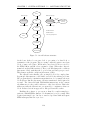
7 System software
7.1 Software structure . . . . . . . . .
7.1.1 Overview of structure . . .
7.2 Module descriptions . . . . . . . .
7.2.1 IIOF3 interrupt . . . . . . .
7.3 Software changes . . . . . . . . . .
7.3.1 Immediate software changes
7.3.2 Future software changes . .
8 Performance
8.1 Current system state . . . . . . . .
8.2 Current system performance . . . .
8.2.1 Envelope function test . . .
8.2.2 Downconverted data . . . .
8.2.3 Fast Fourier Transformation
8.2.4 Processing of a signal . . .
8.2.5 Processing load . . . . . . .
.
.
.
.
.
.
.
.
.
.
.
.
.
.
.
.
.
.
.
.
.
.
.
.
.
.
.
.
.
.
.
.
.
.
.
.
.
.
.
.
.
.
.
.
.
.
.
.
.
.
.
.
.
.
.
.
.
.
.
.
.
.
.
.
.
.
.
.
.
.
.
.
.
.
.
.
.
.
.
.
.
.
.
.
.
.
.
.
.
.
.
.
.
.
.
.
.
.
.
.
.
.
.
.
.
.
.
.
.
.
.
.
.
.
.
.
.
.
.
.
.
.
.
.
.
.
.
.
.
.
.
.
.
.
.
.
.
.
.
.
.
.
.
.
.
.
.
.
.
.
.
.
.
.
.
.
.
.
.
.
.
.
.
.
.
.
.
.
.
.
.
.
.
.
.
.
.
.
.
.
.
.
.
.
.
.
.
.
.
109
109
109
111
113
116
116
117
.
.
.
.
.
.
.
119
119
120
120
122
122
123
123
9 Conclusion
125
A Explaination of EXCEL timing sheet
129
B Specifications for Pentek 6441 ADC
133
C Specifications for Pentek 6510 DRX
134
D TMS320C40 block diagram
136
E HP48G/GX program for TI floating point conversion
139
F Source code: set ivtp.asm
140
G Source code: iiof3.asm
143
H Source code: dmaintx.asm
145
I
Source code: dma.asm
147
J Source code: wait.asm
150
K Source code: process.c
152
L Source code: window.asm
153
M Source code: cr2dif.asm
156
N Source code: accu.asm
161
4
CONTENTS
CONTENTS
O Source code: incBR.asm
163
P Source code: dis dma.asm
164
Q Project timetable
166
5
CONTENTS
0.1
0.1. PREFACE
Preface
This report is written by me, Kristian Philip JØRGENSEN, and it is the
documentation of my master’s degree project.
The project is carried out at CERN in Switzerland/France for the Technical University of Denmark (DTU). The supervisor in Denmark has been
Associate Professor Jan LARSEN, from the Section for Digital Processing,
Department of Mathematical Modelling (IMM). The supervisor at CERN
has been Flemming PEDERSEN, the section leader of the PS division low
level RF section.
This report is written for people with a basic engineering background.
No specific knowledge in accelerator physics, signal processing or programming, is required in advance. It has been the intention to explain all involved subjects of science, in order not to keep any potential reader from
understanding the content of this report. This is basically because the
environment at CERN consists of a mixture of physicists, engineers with
different back grounds and techniciens, all working together with the same
goal. This report is adapted to this interdisciplinary environment.
This report is written in LATEX for better readability, mostly concerning
equations. Everything is written by me, whenever there is some material
taken directly from another source, it will be clearly mentioned. The figures
in the report is either drawn by me in XFIG or picked from referenced
material listed in the bibliography.
The notation in this report is aimed to be consistent. Whenever a reference to a book is done it is written as a number in square braces, []. All
references are listed from page 126. References to tables, figures, chapters,
sections etc. is referenced by the number written, when they are introduced.
Only when a reference is far away from its mentioning, the page reference
is written. All abbreviations are introduced with their complete list of
words before their first use, but afterwards written abbreviated without
additional information. The numbers used in the text are by default with a
base of 10. Whenever they are different or in case it needs to be clear, their
base are written as subscripts, DEF AU LT10 , BIN ARY2 , HEXh . Signals
in continuous time domain uses t for time, discrete signals n. In the continuous frequency domain f is used for frequency and in the discrete k. The
reversible Fourier transformation between these two domains are denoted
↔. Whenever a [Schaum number] is written after an equation, it refers
to [7] with number as equation number. Words from accelerator physics
isboldfaced when first mentioned, to facilitate re-look up. When a program call is merged with text it is written in italic. When the program
code is written entirely, then it is in small letters format. To facilitate the
reading of this report, the use of footnotes1 is introduced.
1
This is a footnote
6
CONTENTS
0.2. ACKNOWLEDGEMENTS
The project started the 15th of January 1998 and this report has been
handed in the 16th of November 1998.
0.2
Acknowledgements
First of all, I am greatly grateful for the possibility of performing my master’s degree project, for the European Laboratory of Particle Physics,
CERN, in France/Switzerland. This is both to the Technical University
of Denmark, DTU, which let me perform it abroad and to CERN which
made it possible.
I would like to thank Flemming PEDERSEN, the section group
leader. His dedication to this project, has been remarkable. Even nearly
drowned in work, he practically always had a minute. But a minute which
frequently became an hour or more. His insight in a wide range of engineering sciences is astonishing. Thank you for letting me profit from this.
Thankyou Nick Vinod CHOHAN for believing in this project and
giving us a helping hand whenever you could. The contacts with you has
been very professional and good for the progress of the project.
Another thank to my supervisor in Denmark, Jan LARSEN, for making a project abroad possible and for distant consultation via email. Especially the project extension, which required quite some writing back and
forth.
I want thank Maria-Elena ANGOLETTA, for the hours we have
worked with the system. You have a high level of knowledge in programming and it has been interesting to solve the numerous system malfunctions,
with you.
A personal thanks to, Silvia GRAU for understanding and support
during stressful periods of the project. As well to all of my friends that I
have made around Pays de Gex and the city of Geneva, your company has
been very nourishing.
7
CONTENTS
0.3
0.3. ABSTRACT
abstract
This report covers the development of an embedded VME crate
data acquisition and processing system. The system is meant
for processing of detected transverse and longitudinal beam signals, from the AD synchrotron at CERN. The sampled beam
signal data rate is close to 2 giga samples per second, so state
of the art processing hardware combined with signal processing
principles is used. A frequency band of interest is downconverted by a digital receiver (Pentek 6510) and a digital signal
processor (TMS320C40) processes data, in an real-time fashion.
The code in the digital signal processor is optimised for speed,
in order to meet real-time processing constraints. This is done
by writing a mixture of assembly and C code.
8
Chapter 1
Introduction
This chapter starts out with an introduction of the project scope. Following
is an introduction to the environment at CERN. Some of the activities and
key features of the organism is mentioned. The group, in which this project
has been carried out, is introduced in the section following.
1.1
Scope of project
The scope of the project, can be boiled down to a short sentence which
coincides with the project title.
”Digital Signal Processing on Schottky Signals”
This includes quite a lot of tasks. First of all there is the understanding
of the signal source which originates from physical processes. This understanding is essential, in order to implement the right processing tasks.
Then there is detection of signals transforming the physical quantities into
electronic signals. This is done elsewhere, thus only a peripheral knowledge
is required. The main part of the project is the acquisition and processing
of these electric signals. This comprises everything concerning development
of such a system. The main part of this project can thus be defined more
specific as following.
Design of an embedded VME-crate-based real-time
acquisition and processing system for power spectral
density analysis of signals from four independent parallel sources at high data rates.
9
CHAPTER 1. INTRODUCTION
1.2
1.2.1
1.2. PROJECT ENVIRONMENT
Project environment
CERN
CERN is the European Laboratory for Particle Physics originally an abbreviation for the french, Centre European de la Recherche Nuclaire. It is the
worlds biggest particle physics centre founded in 1954. The 12 european
member states all financially contribute to the research and the annual budget is around 600 million US dollars. The member states contribute with a
certain percentage and this should correspond to the percentage of employees from the member states, taking part in the work at CERN. There are
around 3000 employees payed directly by CERN and 6500 scientists using
the facilities at CERN.
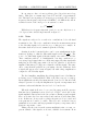
The overall goal of CERN is research of particle physic and for this is
used rings for accelerating, decelerating and storing particles for different
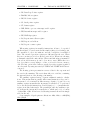
purposes. The largest one of those rings are 27 kilometres (LEP1 ) on both
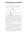
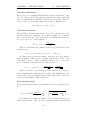
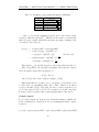
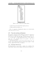
swiss and french territory, see figure 1.1. It is situated 100 meters beneath
the ground surface and the 4 detectors are of the size of four storey houses.
Particles travelling along this 27 km. circular accelerator travels near the
speed of light, this means that they make around 11.000 rounds per second.
This and other tasks require highly specific equipment which only finds its
use at CERN. That is why a lot of development is done at these premises.
As an example, CERN has a magnet in an accelerator which weighs more
than the Eiffel tower in Paris.
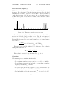
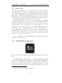
Figure 1.1: Left:CERN seen from above. Right: A particle detector.
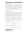
In some circular accelerators two beams collide in particle detectors.
1
Large Electron-Positron collider
10
CHAPTER 1. INTRODUCTION
1.2. PROJECT ENVIRONMENT
This is to discover what mass is made of. The particles are broken into
their components and their trajectory are measured by the particle detectors. One of the quests of this decade is the search of the Higgs particle,
which should exist, but this is never verified. The resolution of the particle
detection rises with the momentum of the particles. That is why the bigger the accelerator the better. The particle detectors are high technology
constructions. They measure among others the trajectory of particle components, from which their mass and polarity can be calculated. The data
acquisition from some particle detectors are astronomical. Some of these
particle detectors have data rates which would be equivalent to the event
that every person on earth, would make 10 telephone calls, simultaneously.
The task of making this possible employs a lot of engineers. Moreover the
data from these experiments should be accessible for scientists on an on-line
basis.
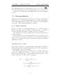
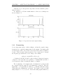
Figure 1.2: Beam collision
Other experiments with particles are done at rest. This means that
special particles are created at high energies and then decelerated in a
circular decelerator. They are then let out of the ring and held in something
called a Penning trap.
Even though the purpose of CERNs activities are particle research there
is development in a lot of other fields. The World Wide Web, for example,
is developed at CERN for the purpose that physicists could share data from
experiments instantaneous, now matter where they were.
As CERN is a research centre there is a lot of publishing and lectures
on recent discoveries and new experiments. These are in all areas of CERN
activities, but with a majority in the area of physics. CERN is, as well,
a place chosen for a lot for conferences. These conferences vary from basic accelerator theory to highly specific areas of physics. Conferences are
mostly free for people working at CERN, but normally open for people
11
CHAPTER 1. INTRODUCTION
1.2. PROJECT ENVIRONMENT
from outside CERN.
A good popular explanation of CERN activities and particle accelerators is explained at the CERN homepage at:
http://www.cern.ch
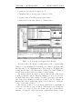
1.2.2
Introduction to the PS/RF
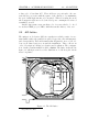
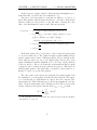
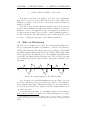
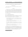
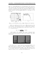
The PS/RF group is the radio frequency group in the PS2 department.
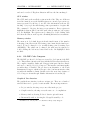
The RF group is responsible for more than 50 different RF systems in the
PS complex, see figure 1.3. The group is further divided into three minor
groups which are:
• Low Level RF
• High Power RF Circular Machines
• High Power RF Linacs and RFQ
The frequencies worked with in the RF group ranges from 0.6 MHz to
3 GHz and the powers from milliwatts to megawatts. This project is done
in the Low Level RF group. The project doesn’t touch the high region of
radio frequencies, but the equipment developed in this project tests that
other modules that do, is working properly.
Figure 1.3: The PS complex
2
Positron Synchrotron
12
CHAPTER 1. INTRODUCTION
1.2. PROJECT ENVIRONMENT
One of the challenges of the group is the AD project of which this project
is a part. The AD project involves RF ”gymnastics” in order to control
the beam with less resources. The AD project is due to finish around April
1999.
13
Chapter 2
Accelerator physics
Accelerator physics is a complicated matter for engineers, not having to
do with physics normally. This project, however, needs to introduce some
basic properties from the accelerator physics, in order to introduce the
problem which this project is supposed to solve. There is quite a lot of
specific terms and properties which are introduced in this section. The
introduction is brief and can be skipped by persons familiar with general
accelerator physics. A complete description of the processes is outside the
scope of this report, but for further details see [3, 5, 4, 6]. The important
terms introduced is boldfaced when explained,to facilitate re-look-up.
2.1
Reason for the AD project
The AD1 project is meant to replace the older method of producing and
decelerating antiprotons for antiproton experiments at rest. This new configuration only involves a single synchrotron, the AD, for the collection,
cooling and deceleration of antiprotons. Previously, 4 synchrotrons where
used to fulfil the same function, namely the AC2 , the AA3 , the PS4 and
the LEAR5 . This is a restructuring of the AC, to a new configuration, AD,
which will lead to a more economical way of producing antiprotons. In
addition it will be a lot faster to produce them. The economical factor lies
in the fact that the former installations needed large amounts of electrical
power, to produce the magnetic fields for the previously used storage rings
AC and AA. The electrical power was an expense of 16-20 Million Swiss
francs6 per year. The new AD synchrotron only operates at full field with
1
Antiproton Decelerator
Antiproton Collider
3
Antiproton Accumulator
4
Proton Synchrotron
5
Low Energy Antiproton Ring
6
Which is approximately equal to 13-17 Million US dollars
2
14
CHAPTER 2. ACCELERATOR PHYSICS
2.2. AD LATTICE
a duty cycle of less than 16%. These fields are proportional to the current and the power rises with the square of the current, so by minimising
the period with high currents, a lot is gained. When decreasing the areas
where magnetic fields are needed, the total power consumption is reduced
remarkably, as well.
Another important reason was that a lot of resources had to be freed
for another CERN project, LHC7 , which has another history of its own.
2.2
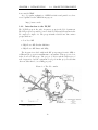
AD lattice
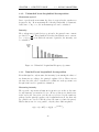
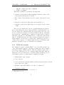
The antiproton decelerator (AD) is a synchrotron, which consist of a vacuum chamber where the particles are guided by specific cells, with magnetic
and electrical fields. These fields insures that all particles, more or less, follows a well defined trajectory around the installation. These cells are in
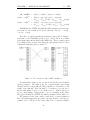
order of description, bending, acceleration and focalisation. The configuration of such a circular machine is called a lattice. The lattice is sketched at
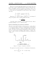
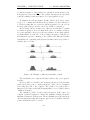
figure 2.1, which gives an idea of the distribution of cells along the 182.43
meter long lattice.
Figure 2.1: The AD lattice
7
Large Hadron Collider
15
CHAPTER 2. ACCELERATOR PHYSICS
2.2. AD LATTICE
Additional information about the synchrotron structure can be found
at [5] and [3]. Specific information about the AD project is described in
[4].
Bunch
The particles can circulate in two modes bunched or unbunced. The
unbunched is with random positions along the trajectory, whereas bunched
is when the particles are kept together by horizontal electric forces.
Synchronous particle
The synchronous particle is an abstract reference particle that perfectly
follows the designed trajectory. The synchronous particle has the same
trajectory in every turn and the trajectory coincide with what is called
the closed orbit. If there are no coherent oscillations among the particles
travelling together in a bunch, then the synchronous particle coincide with
the centre of massof the bunch.
Betatron/Synchrotron oscillations
Practically no particles follows the closed orbit perfectly, there is always
some oscillation about this orbit, of minor or larger amplitude. The transversal decomposition of such a 3 dimensional motion is called the betatron
oscillation. A longitudinal decomposition of the oscillation is called the
synchrotron oscillation. The betatron oscillation is also denoted the
tune and it is given as Q = fbetatron
frev . The respective cells affect either the
betatron or the synchrotron oscillation. No cell affects both, so these two
decompositions can be considered as being uncorrelated.
These two quantities are of great importance to the project, please make
a note of them.
Vacuum chamber
The beam travels inside a vacuum chamber, which is held at a very low
pressure to avoid the particles from colliding with gas molecules. In the
former AC configuration the total pressure in the vacuum chamber was
around 8 pbar., This is equal to a total molecule density of less than 1015
[Molecules/m3]. The vacuum conditions for the AD configuration has to
be improved 20 times.
Energy
The particles have a total energy that can be divided into two contributions,
the kinetic, T , and the energy at rest, E0 , E = T + E0 . The energy at rest
16
CHAPTER 2. ACCELERATOR PHYSICS
2.3. CELLS IN THE LATTICE
is calculated as E0 = m0 c2 , where m0 is the mass at rest and c the speed of
light. As the velocity of the particle rises, it gains more kinetic energy. The
contribution from the kinetic energy is, T = (γ − 1)E0 . γ is the relativistic
factor given as
1
m
=
γ=
2
m0
1− v
c2
- where v is the velocity of the particles and m the relativistic mass. It can
be interpreted as , the factor that the mass of a particle, gains by having a
velocity. In classical mechanics the formulas are similar , only the velocities
are very small compared to the speed of light, so the γ factor is close to 1.
Approaching the speed of light makes γ approach infinity and the kinetic
energy becomes significant compared to the rest energy. Close to the speed
of light the velocity of a particle changes very little, as result of rise in total
energy. The rise in energy level is stored as extra mass in stead. This is
why the particles are never accelerated to the speed of light, this would
require disposal of an infinite energy source. The quantity that gives the
ratio between the velocity and the speed of light, is called β, β = vc .
The momentum of a particle is, p = mv = γm0 v. It is measured in
[eV /c], thus multiplied by c we have pc with the dimension of energy. In the
normal SI8 system, energy has the dimension Joule, [J], but in accelerator
physics the unit electron volts, [eV ] is used, as it is closer to the related
motion. One electron volt is defined as the energy an electron gains, by
accelerating through a electrical potential of one volt. Likewise, we can
calculate the mass as being proportional to energy by multiplying with c2 .
As an example, a proton (and antiproton) has the mass
m0 = 1.670 10−27 [kg] = 938 [M eV /c2] ⇒ m0 c2 = 938 [M eV ]
This way a comparison is possible and at certain velocities v → c the
contribution from energy at rest can be neglected.
The formulas for relativistic calculations mentioned above, can be summed
up in table 2.1. These formulas are used in later sections, without reference
to the table 2.1.
2.3
Cells in the lattice
Bending Magnets
Bending is the action that accelerates the particles horizontally, towards the
centre, so that they describe a circular loop. By using uniform magnetic
fields, normal to the velocity, the particles are subjected to a force, that
8
Standard Internationale
17
CHAPTER 2. ACCELERATOR PHYSICS
2.3. CELLS IN THE LATTICE
Table 2.1: Relativistic formulas
Total Energy
Rest Energy
Kinetic Energy
Momentum
Relativistic Factors
E = T + E0 = γE0
E0 = m0 c2 ,
T = (γ − 1)E0
p = γm0 v
γ = mm0 = EE0
β = vc
E ≈ pc for velocities near c
E0 = 938[M eV /c] for a proton
1<γ<∞
0<β<1
makes them accelerate towards the centre. The momentum derivative is
described by Lorenz as:
dp
= e(E + v × B) = F
dt
- where e is the charge, F is the force vector.
Having a vertical uniform magnetic field and a trajectory completely in
the horizontal plane. Using a system of coordinates with s as a tangential
vector along the curvature, x as horizontal component and z as vertical.
The equation can be reduced and split into the 3 components:
(px , ps , pz ) = e(vs Bz , 0, 0)
,which describes a circle trajectory with radius,
ρx =
ps
γmvs
=
[m].
|e|Bz
|e|Bz
The uniform magnetic field is obtained by a magnetic dipole.
The momentum is proportional to the bending radius, ρ , in the magnetic field, B. The strength of the magnetic field is inverse proportional
to this radius. In a synchrotron the magnetic field and the momentum
is synchronised, |p| ∝ |B| , thus resulting in conservation of the bending
radius.
This principle has a great advantage. It limits the trajectory of the
beam to be a closed loop, in stead of a spiral as in cyclotrons.
In the AD lattice there are 24 of those bending magnets, each of them
◦
taking care of 15◦ ( 360
24 ) of the bending angle.
RF cavities
The velocity of the beam is controlled by RF9 cavities. They have two
functions, to accelerate/decelerate a bunch and to divide and keep the beam
9
Radio Frequency
18
CHAPTER 2. ACCELERATOR PHYSICS
2.3. CELLS IN THE LATTICE
divided in bunches. This cell has an impact on the synchrotron motion of
the beam. A simple cavity is a plate with a hole for passages of particles. Between the plates there is a voltage resulting in an electrical field
between the plates. With alternating voltages, at radio frequencies, connected to the plates, it is possible to focus the particles longitudinal around
the synchronous particle. The voltage (V = Vplate1 − Vplate2 ), between the
plates, are sinusoidal and varies with time as, V (t) = V0 sin(2πfRF t). The
hvs
is a multiple of the revolution frequency
radio frequency, fRF = Lclosed
orbit
fRF = hfrevolution , where h is the integer number of bunches along the
closed orbit, Lclosed orbit the length of the closed orbit and vs the velocity
of the synchronous particle.
For the AD synchrotron, the length is 182.43 meters. There is 1 bunch
(h=1) and to start with, the particles are travelling with the speed that is
96.72% of the speed of light (γ = 0.9672).
Thus this system needs an RF frequency of:
1 × 0.9672 × 2.9979 108
hvs
=
= 1.59 [M Hz]
L
182.43
At each passage of the RF cavity, the particles are either accelerated,
decelerated or neither. The change in longitudinal kinetic energy is given
as:
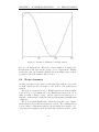
∆Es = qV0 sin(φs )
fRF =
- where φs is the phase of the arriving synchronous particle, in respect to
the RF frequency, and ∆Es is the synchronous energy gain per turn. This
gain corresponds exactly to the change of the strength, in the magnetic
field, B.
There is a small dispersion of phases in the bunch of particles, so not
every particle is arriving with this phase, nor the same energy. For a
non-synchronous particle, with an energy difference in respect to the synchronous particle of ∆En , the energy difference after passage becomes:
∆En+1 = ∆En + |q|V0 (sinφn − sinφs )
so if the phase, φn is bigger than φs (but still smaller than π − φs ) ,then
the energy difference, compared to the synchronous particle , will grow. But
in a stable case, the phase will decrease within the next iteration. The next
iteration will have another phase and thus another change in the energy
level. The result is a trajectory about the synchronous phase, φs , which is
closed for phases, φn , that doesn’t exceed π − φs for zero value energies,
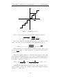
∆En , (see figure 2.2).
For small variations the trajectories are close to circles, for larger amplitudes they take form as fish-like trajectories. The largest possible trajectory
that insures stable longitudinal synchrotron oscillation is called the separatrix or bucket. A particle moving along coordinates (∆En , φn ) outside
19
CHAPTER 2. ACCELERATOR PHYSICS
2.3. CELLS IN THE LATTICE
this closed trajectory will follow an open trajectory and is unstable.
If the differences in phase are too significant, then the rise in energy level
will be big. Particles may then not be bent enough, by the bending magnets, and they will follow a trajectory along a slightly larger circumference.
Then they will follow a longer route and they wont be able to catch up with
the synchronous particle, in spite of their rise in total energy. Such unstable
particles will grow in both phase and energy difference. Eventually they
will be lost, due to geometrical limitations of the vacuum chamber. These
are the particles that follows the open trajectories outside the separatrix.
Figure 2.2: Synchrotron motion in phase plane
Quadrupoles
If ideal fields were available, there would be no need of focusing the beam
onto its orbit. But due to imperfections, in the fields, the beam is not kept
together automatically. Small variations in the particles grows and if no
step towards dispersion were taken, it would not be possible to conserve a
beam, in a storage ring, for very long time.
A weak focusing force can be implemented, by adding a gradient to the
guiding magnetic field. This way a vertical focusing could be obtained.
In the bending magnets a gradient could be added to insure horizontal
focusing. This is possible but large volumes of magnetic fields are required.
A better focusing mechanism has thus been invented. By adding what
is called an alternating gradient or a strong focusing force, it is
possible to obtain small amplitudes of the betatron oscillations. Thus a
smaller beam dimension is needed, which also makes it possible to raise
the magnetic field along the orbit. Thereby, both higher energy and higher
beam densities, can be obtained.
This force comes from focusing magnets called quadrupoles. They
consist of four poles, constructed in a way that the centre of the magnet,
20
CHAPTER 2. ACCELERATOR PHYSICS
2.3. CELLS IN THE LATTICE
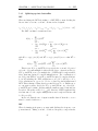
has no magnetic field and the field is rising linearly, with the displacement
from the centre (see figure 2.3).
North
South
South
North
Figure 2.3: Quadrupole focusing horizontally for antiprotons going into the
paper
There are two types of quadrupoles, only difference is the orientation of
the poles. They are respectively flipped 90 degree clock or counter-wise to
one another. This results in gradient fields that are successively focusing
along one axis and in the next focusing along the other, 90 degree flipped
axis.
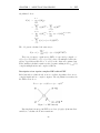
Figure 2.4: FODO cell
Looking at only one component , say the horizontal axis, a particle
meets a focusing magnet (F) that pulls the particle towards the centre of
21
CHAPTER 2. ACCELERATOR PHYSICS
2.3. CELLS IN THE LATTICE
the quadrupole. During the subsequent piece of orbit, there is no focusing
forces/effects involved(O). Then the particle meets a focusing force in the
vertical component, but due to the flipped structure it is now defocused in
the horizontal plane(D). The defocusing is proportional to the displacement
from the centre of the quadrupole and as the beam is smaller horizontally
at this location, defocusing will not be as strong as focusing. The lattice
is then build up of a system of these quadrupoles in a, so called, FODO
pattern. Such a pattern has successively changing magnet polarities. The
AD lattice has 28 such FODO cells. 56 times during rotation the angle,
with respect to the closed orbit, of the particle is changed. This eventually
results in transversal oscillations around the orbit.
The motion around the transversal plane is somewhat discrete, as the
cells result in almost instantaneous changes and the change of displacement
is linear with time. The normalised frequency of these transverse betatron
oscillations are denoted Q. This is the frequency in respect to the revolution
). It is also sometimes denoted the tune of the
frequency,( Q = fbetatron
frev
beam. In the AD lattice, the betatron oscillations has Q values in the
horizontal plane of Qh = 5.39 and in the vertical plane Qv = 5.37. So these
particles with a Q in the neighbourhood of 5.3 needs approximately 11 (≈
56
5.3 ) passages of quadrupoles, to perform one single oscillation. The analogy
to lenses, as shown on figure 2.4, are thus an example fairly simplified.
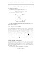
The displacement is more like on figure 2.5 , here there is 76 changes of
derivative, which is similar to sampling the position after each quadrupole.
This is a typical path for the particles.
The analysis of cells affecting the beam trajectory, is however called the
optics because of the similarities with lenses.
Kicker magnets
The kicker magnets are used to inject or eject a beam from the lattice.
This is a dipole magnet, with steep rise and fall time, insuring rapid change
of beam trajectory. The reason for having this cell, is that the bending
magnets has strengths of fields that do not easily enable rapid changes. So
the magnetic fields of the bending magnets are conserved and in stead the
beam, or part of it, is guided passed the bending magnets.
Stochastic cooling
Stochastic cooling is performed when the emittance has to be brought
down. This is only one of the many ways of cooling the beam (electron
cooling, laser cooling etc.). It is done by measuring a fraction of particles,
n, of the total amount of particles, N . As the number measured is much
less than the total number, n << N , it is more likely that the particles
22
CHAPTER 2. ACCELERATOR PHYSICS
2.4. BEAM DYNAMICS
Figure 2.5: Betatron oscillation for a single particle
have a local displacement. Whereas for larger number of particles the
measurement would approach the average of zero displacement. Kicking
towards the orbit can eventually eliminate the mean displacement, of these
n particles. The total emitance thus decreases.
2.4
Beam dynamics
Creating a moving reference frame, for the particle(s), with the closed orbit
as origin, enables an easier description of the motion of the particle(s) in
rotation.
The motion of particles is close to Hamiltonian motion. This is similar
to the motion of a pendulum, where the Hamiltonian energy is stored as
either potential or kinetic energy. As the particles aren’t subjected to
resistance on their travel, ideally, they will perform undamped Hamiltonian
oscillations.
The motion is thus Hamiltonian oscillations along three axes, longitudinal, transverse horizontal and transverse vertical. The resulting motion
is some bizarre 3 dimensional path about the synchronous particle. Decomposing and treating the motion in these three planes is possible, as the
23
CHAPTER 2. ACCELERATOR PHYSICS
2.4. BEAM DYNAMICS
lattice is build so that motion in one plane, does not have influence on the
others.
In the longitudinal plane the delay of a particle along the closed orbit, in
respect to the synchronous particle, is denoted τi . The particles will perform
a sinusoidal oscillations about the synchronous particles. The delay will,
ideally, follow the equation:
τi (t) = τ̂i sin(Ωs t + Ψi )
, which follows the synchronous particle in mean, but has sinusoidal
fluctuations about it. At a flash in time, the particle has thus a delay
in respect to the synchronous particle, but also a different level of kinetic
energy. That is, the particle might be behind or before, but accelerates so
it eventually approaches the synchronous one (stable state). The resulting
motion is best shown in a phaseplane. The difference in phase from the
synchronous particle as first axis and difference in energy level, ∆E, as
second. In this plane the motion will be a ellipsoidal motion about the
origin. The origin is a fixed reference, being the synchronous particle.
In the transverse horizontal and transverse vertical plane, the same axes
are used. First axis is the displacement from the closed orbit and second
the derivative of the displacement, hence velocity. As before we decompose
the movement in a horizontal and a vertical plane. The oscillation, about
the orbit, will in this system, as well, be described as an ellipsoidal motion
about the origin in both these two phaseplanes.
For the same example as used prior to this section, a plot of 76 passages
of quadrupoles is shown on the figure 2.6.
The solid line is the complete movement of particles, whereas the dotted
line is drawn from discrete samples after each FODO cell.
2.4.1
Motion contributions
The cause of these movements in the three planes, can be decomposed
into several linear contributions. The bending, the acceleration, the
focalisation and the non-active straight sections of the lattice.
The action of acceleration has an effect on the longitudinal phaseplane. By passage of the accelerating cell, the particle increases its kinetic
energy (upwards in phaseplane) almost instantly. Within the section between the next accelerating cell, it increases the phase, φ(t). This will create
a somewhat bizarre path about the origin, made of sections of straight lines
in the longitudinal phaseplane. These lines are quite small, compared to
the circumference of the trajectory around the phaseplane.
The action of focalisation is likewise described by an almost instantaneous change of angle, in respect to the closed orbit. In between the
24
CHAPTER 2. ACCELERATOR PHYSICS
2.4. BEAM DYNAMICS
Figure 2.6: One betatron oscillation in the transverse phaseplane
focalisation cells, the displacement rises or falls linearly with time. Again
the product is a straight lined path about the origin.
The effect of the bending is not meant to have influence on any these
phaseplanes, but due to imperfections of the uniform magnetic fields, this
is inevitable. Of course, if bending magnets with gradients in the magnetic
field are used then, as described in the weak-force focusing system, it would
have an effect on the transversal planes as well.
The non-active straight sections do not change the velocity or energy. In all planes, this can be described by a straight horizontal line, hence
no changes in energy nor angle.
The amplitude of the motion in each of the 3 phaseplanes can be described in terms of the emittance, 3. This is the area that the particles
surrounds, by their path (measured in [π mm mrad]). It is similar to the
standard deviation, σ, of the particle from the closed orbit. All particles described in the same phaseplane, gives the total emittance of the beam. The
emittance is inverse proportional to the momentum, so when accelerated,
the emittance decreases as 1p . This is called adiabatic damping. However,
25
CHAPTER 2. ACCELERATOR PHYSICS
2.4. BEAM DYNAMICS
as a consequence of decreasing the momentum, as in the AD, the emittance
rises in stead. The normalised emittance is given as 3N = βλ3, and is independent of the momentum. According to the theorem of Louville, this
normalised emittance is conserved as long as no cooling is performed. The
95% emittance of a beam, is defined to contain 95% of the particles. That
is, 95% of the paths can be drawn within this area, see figure 2.7. Typical
values for the emittance of the beam, in AD lattice, is in the neighbourhood
of 5 [π mm mrad].
Figure 2.7: Snapshot of Particles in the Horizontal Transverse Phaseplane
2.4.2
Beam instabilities
The beam instabilities is a science of its own. Quite complicated matters can make the beam instable and it would be outside the scope of this
project, to cover them profoundly. A short introduction to the most important causes of instabilities is introduced here.
In the preceding section, the paths were described as were they only
determined by the effects of magnetic fields. There is another effect from
the residual gases in the imperfect vacuum of the beam chamber. There
are still collisions with these gas molecules, which results in scattering of
the particles. Three types of collisions can occur , single coulomb, multiple
coulomb and nuclear scattering. They all contribute to disjunctive changes
of the movement about the phaseplanes. If their changes are too big, then
the system is not able to recover the control of the particles. Smaller variations are not fatal, due to the beam control actions mentioned above.
A far more important factor is beam resonance, this leads to loss of
the whole of the beam. The resonances occur when the beam fulfils the
equation
nQ = p
26
CHAPTER 2. ACCELERATOR PHYSICS
2.4. BEAM DYNAMICS
- where n and p are integers. The lowest order resonances, low n values,
are the strongest and most destructive. As the order rises the importance
declines and higher order than 5 can, as a rule of thumb, be neglected.
The combination of horizontal and vertical tunes can lead to resonance,
as well. This occurs in the same way, when the tunes reach values which
fulfils the following equation.
nQh + mQv = p
- where n, m and p are integer values.
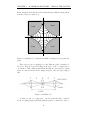
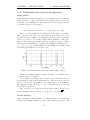
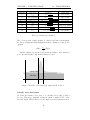
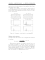
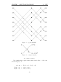
In a plane with the horizontal and vertical tunes as axis’, the instability
lines takes shape as on figure 2.8. The single resonant is shown up to 5th
order, with solid lines. The combined up to 3rd order with dotted. The
position of the point (qh , qv ) should be far from resonances as possible,
thus placed far from lines. The Schottky analysis allow us to zoom in on a
square which is 0.1125 × 0.1125, shown as punctured line on figure 2.8. The
q values are presumed to be in the middle of this square. They should not
coincide with the strong 3rd order resonance, at 5.33, nor the 5th order, at
5.4. These are the most important ones to avoid.
Figure 2.8: Resonant tunes
The reason why this equation leads to instability is, that the beam has
a tune that becomes a fraction of the revolution frequency. This means
subsequent passages of the same spots. A tiny imperfection is then accumulated thousands of times and even a tiny contribution, will in an instant,
result in an unstable non-recoverable oscillation.
27
CHAPTER 2. ACCELERATOR PHYSICS
2.4. BEAM DYNAMICS
The Q values can be changed by adjusting the quadrupole magnetic
field. The Schottky analysis is an important tool for this adjustment. It is
important to know the current q value, in order to know what to change. To
begin with, the q values are given by calculations and complex simulations.
The values are currently at, Qh = 5.39 and Qv = 5.37.
2.4.3
Matrix representation
A frequently used method of calculations on a synchrotron lattice optics is
to divide each section or cell independently. The parameters are the incom0
ing displacements and velocities, say [x0 , dx
dt ] and change of the parameters
after the passage of the section or cell [x, dx
dt ]. This can be represented in a
dx0
dx
matrix form as: [x, dt ] = T [x0 , dt ], where T is a 4 × 4 transport matrix
and ’ is the Matlab notation for transponed. T can be a transformation
matrix, consisting of either functions or simply numbers. It depends on
both the architecture of the cell and the type. A single straight section
with no magnetic fields has a transformation matrix as T = [ 1 l ; 0 1 ]
where again ; is Matlab notation for new row and l is the length of the
section. By multiplying together all matrices in the ring, a total transformation matrix, say S, for the system is calculated. This matrix should not
n
divert when lifted to a high order, (S for n → ∞). This would mean that
the system was unstable.
Some more sophisticated methods are using vectors containing the normalised change in momentum as well, for the horizontal phase plane this
∆p
becomes [x; dx
dt ; p ]. Such analysis’ are always done by optical simulation
programs.
2.4.4
AD cycle
The anti-protons, in the AD, are produced from a 26 [GeV /c] beam of
1013 protons. The protons hit a target of iridium and after the coalition,
antiprotons, at different energies, are produced. The antiprotons, with a
momentum of around 3.5 [GeV/c], are collected. This is an injection of
about 5 107 antiprotons . Their energy corresponds to a start revolution
frequency of 1.587 [MHz]. This corresponds to a velocity close to the speed
of light. Then the beam is bunched to avoid momentum dispersion, this
dispersion is decreased from ±3% to ±1.5%. The beam is then stochastically cooled to an emittance of 5 [π mm mrad]. The beam is decelerated
to 2 [GeV/c], where it is cooled to avoid adiabatic beam blow up. Then
again decelerated and cooled with electron cooling. The beam is then extracted from the synchrotron to experiments. The number extracted is
about 1.2 107 , thus an efficiency of about 25%, in respect to what is injected.
Combining the formulas p = γm0 v and fr = Lv reveals
28
CHAPTER 2. ACCELERATOR PHYSICS
1
fr = p
L
2.4. BEAM DYNAMICS
c2 p2
c2 m2o + p2
from which the revolution frequencies are calculated.
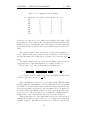
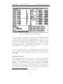
f_r [Mhz] p [GeV/c]
Injection
1.587
3.5
1.488
2.0
20 s
15 s
Extraction
0.501
0.174
6s
0.3
0.1
10
33.5
52.5 60
70
Bunched mode
Stochastic Cooling
Figure 2.9: Beam state steps in the AD
29
time [s]
Chapter 3
Schottky Noise
In this chapter, the Schottky noise will be introduced. The chapter is
strictly theoretical, containing quite a lot of mathematics and signal analysis. Only the principles of signal behaviour is introduced. Considering
the complete signal behaviour would involve too many parameters, to be
performed in a nice analytical way. Such complete analysis’ are left for the
simulators to do.
At first the signal source is introduced, then the way it is detected.
Following is a the main part of this chapter, going through the analysis of
these four types of signal. The system noise contributions to these signals
is only just mentioned. Then the signals are analysed from a power spectral
density point of view. This including the effect of a noise floor. This part
is statistical and considers the effect of averaging spectra. The windowing
function is introduced and the effect of it, applied to the power spectral
density calculation. Finally the timing of such signal detection, is gone
through. This finishes with a sheet containing a draft of the analysis timing.
3.1
What is Schottky noise
The name Schottky noise signal, is a bit misleading. It is not really noise, as
we are used to think of it. Ordinary noise has uncorrelated nature, whereas
Schottky noise is a bit different. Schottky noise, is an addition of many
coherent signals, but individually uncorrelated in phase and frequency. In
our system the coherent signals appear, when the same particle passes the
same pick-up successively in a systematic way. However about 50 million
other particles are doing likewise, but with no correlation to each other.
Special techniques is thus needed to observe the signal, in order to derive
the Schottky noise information.
We do not detect single particle behaviour, but a kind of very detailed
behaviour of the beam. Each passage of particles does add information that
30
CHAPTER 3. SCHOTTKY NOISE
3.2. SIGNAL DETECTION
could be analysed, if we had equipment that was fast enough. However,
the particles are passing at a speed close to the speed of light, so the detected signal is an integration of a large number of particle passages. This
is equal to a smearing in the frequency domain. So the individual particle
components becomes a Schottky band.
Each band has a bandwidth and it rises with the harmonic number. We
presume a uniform distribution of frequencies, around the revolution frequency, within ∆f and we have N particles. The DC current is N < frev >,
where < frev > is the mean revolution frequency. The first harmonic broadens ∆f , the next 2∆f and so on. The band around the n’th harmonic
becomes n∆f . Eventually the band will overlap, as this is repeated with
identical frequency harmonics and rising bandwidths. Bands with no overlap has an integral that gives information about the number of particles.
This is denoted the intensity. The band also gives information about the
spread in revolution frequencies and the geometric properties of the beam.
3.2
Signal detection
Application specific detectors, denoted pick-ups, are developed to detect
the displacement of the beam, in respect to the synchronous particle.
The longitudinal pick-ups use the fact that a motion of charges induces
a rotating current, in a surrounding material, normal to the particle motion (J = nqv p ). A beam travelling inside a tube, would result in a current
at the inner surface of the tube, proportional to the number of charges in
the beam, but in the opposite direction1 . By introducing a discontinuity
in the tube, the beam gets slightly disturbed, but not significantly. The
current is then not able to pass the discontinuity, but is lead through an
impedance in stead (a coupler). This enables measurement of the beam
current. The principle of the pick-ups used in the AD project, is of this
resistive-gap-type, see figure 3.1.
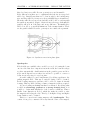
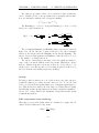
The transverse pick-ups rely on the principle, that a charged particle, in
the middle of a large two plate capacitor, will result in the same potential
on both plates of the capacitor, whereas a small displacement, will have an
impact on both plates (see the later section 3.2.1). So both sign and value
of the displacement, is detected this way. The detection is split up in the
transverse vertical and the transverse horizontal plane.
1
The charges are travelling in the same direction, but are of different polarity
31
CHAPTER 3. SCHOTTKY NOISE
3.2. SIGNAL DETECTION
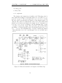
Figure 3.1: Principle of longitudinal resistive gap type pick-up
3.2.1
Charge passage of transverse pick-up
The transverse pick-up consist of two parallel plates, with bended corners.
The length of the pick-up is ∼1 meter.
Image
plate 1
q
+
U
plate 2
Image
Figure 3.2: Cross section of transverse pick-up
When a charge is between the plates, it induces a charge each of the
plates. This can be modelled as having two image charges at each side. The
field lines crosses the plate with a 90 degree angle and creates an induced
charge on the surface. As the two image charges are not of equal value, due
to difference in distance from the charge, there will not be an equivalent
amount of charge on both plates. The voltage between the plates will be
Qplate 1 − Qplate 2
C
The actual induced current, is quite a difficult piece of calculation to
U=
32
CHAPTER 3. SCHOTTKY NOISE
3.2. SIGNAL DETECTION
perform. Normally this is done numerically. A good approximation is to
assume that the voltage varies linear with the displacement from the centre. If the charge is situated at the plates, then the image charge coincides
with the charge and the other plate has no induced current. In the middle
the induced current is zero, as both image charges are equal. In between
we thus assume this linear variation leaving us with the transfer function
visualised in figure 3.3. The solid circles, on the figure, shows the values
where the voltage are exact.
volatage
q/C
-d_max
d_max
displacement
-q/C
Figure 3.3: Charge displacement versus Voltage
When a charge enters the gab of a pick-up, it induces a current on
both plates. When it leaves the pick-up gab, it induces a current of exact
opposite polarity. The spectrum of such subsequent passage is going to
be studied in the following. First we split to signal up into two signals,
corresponding to the entering and leaving, of the pick-up.
current
T
time
T
Figure 3.4: Charge passage
33
CHAPTER 3. SCHOTTKY NOISE
3.2. SIGNAL DETECTION
signal = a(t) + b(t)
The first signal, a(t), is just a repeated δ-function which has a periodic
spectrum of a sinc2 function.
So a(T ) has the spectrum A(f ), written.
a(t) ↔ A(f )
The ↔ symbolises the reversible Fourier transformation. The left side
is the time domain and the right side frequency domain.
Then for the spectrum of b(t) we have the same, only negative, and the
phase of them is a bit displaced in time.
b(t) = −a(t + ∆T ) ↔ −A(f )ej2π∆T f = A(f )ej(2π∆T f +π) = B(f )
The signal sum can then be expressed from only the spectrum of a(t)
as
signal = a(t) + b(t) ↔ A(f )(1 + ej(2π∆T f +π) )
This envelope has an absolute value that vary with the frequency from
0 to 2 and in phase from −π/2 to π/2. In a complex plane, the envelope
follows the trajectory drawn at figure 3.5
6o
1
2
73o
Figure 3.5: Complex envelope
2
a function with nature, sinc =
sin(at)
sin(t)
34
CHAPTER 3. SCHOTTKY NOISE
3.2. SIGNAL DETECTION
In our setup we have a 1 meter pick-up, placed in a 182 meter long
lattice. This gives a constant ratio between T and ∆T of approximately
182. The time between passages, T , is inverse proportional to the revolution
frequency, this frequency vary from 0.174 MHz to 1.56 MHz in the AD. A
rewritten version of the envelope for our system, becomes.
f
1 + ej(2π 182frev +π)
With these two frequency intervals, f and frev , we use only from ∼6 to
∼73 degrees, hence shaded angle interval on figure 3.5.
3.2.2
Noise
The signals are subjected to several noise contributions, before the final
treatment is done. The noise contribution from the measurement system
to the Schottky signals, is beyond the scope of this project to analyse. A
short introduction is, however, summed up in the following.
Starting from the beam itself, there can be some misalignment in the
transverse pick-up, so that the differential signal is added an√offset. The
power of a differential signal (Schottky signal), rises with N and the
offset contributes with N . So misalignment, even tiny, contributes to a
very strong biased signal, that exceeds the interesting Schottky signal with
many factors. The AD beam consist of about 5 107 particles, so an offset is
amplified 7000 times (77 [dB]), more than the Schottky signal. The same
effect occurs when the particles are performing coherent oscillations. Such
a signal will appear as a betatron signal, but with a huge amplification
compared to the Schottky signal.
The head amplifier, amplifying the pick-up signal, is not ideal thus introducing errors of different kinds. First of all, there is never a complete
linear amplification in all of the input interval. Some level of distortion will
always be present. Secondly, the amplification depends on temperature and
resistance values and this introduces a level of coloured noise.
When the signal is all set to be processed it passes an A/D converter
that introduces quantisation noise at a level of ∆V /2n , where ∆V is the
signal amplitude interval and n the bit resolution. Having a random signal
these errors introduced are uncorrelated and random as well, thus white
noise. In this case, however, the revolution frequency is close to fixed and
some patterns are bound to be stable. Thereby some correlation between
quantisation errors arise and larger parasitic frequency components, called
spurious components, occurs.
Taking only the noise from the system amplification into account, one
gets an estimate of the signal to noise ratio, available for treatment. From
35
CHAPTER 3. SCHOTTKY NOISE
3.3. BEAM PARAMETERS
√
the longitudinal pick-up a spectral density noise level of 1.5−2 [pA/ Hz] is
aimed. For the transverse case the spectral density is 0.3−0.5 [pA/sqrtHz].
As the AD cycle changes state, the amplification and noise levels changes,
as well.
3.3
Beam parameters
In this section the signal nature will be introduced. The detected signals are
analysed in order to derive the beam parameters from them. This analysis
is done with signal analysis techniques. It is mostly theoretical calculations
done in the continuous time and frequency domain.
3.3.1
Signal treatment
There are four types of beam signals, that has to be considered. First of
all, the beam can be either in a bunched or unbunched state. Second, there
is both longitudinal and transverse signals detected in both states.
The transverse are split up in vertical and horizontal, but their treatments are similar.
The description of the signal treatment and what we can expect from it
is divided into the four types described above. For additional descriptions
please refer to [1] and [2]. Most of the descriptions are supported by Matlab
calculations and plots.
Unbunched r.m.s. current
Most of the processing is done from unbunched signals and the calculations
is almost identical for longitudinal and transverse case. The only difference
is the amplitude of the detected signal.
The particle pick-up passage is estimated to be very fast compared to
other time constants in the system, so a passage is modelled as a delta
function, δ(t). Each passage occurs with the revolution frequency of the
particle in mention, fi , thus a train of delta pulses.
i(t) = efi
∞
exp(jnωi t + φi )
n=−∞
= efi + 2efi Re[
∞
exp(jnωi t + φi )]
n=1
= efi + 2efi
n=1
36
cos(jnωi t + φi )
CHAPTER 3. SCHOTTKY NOISE
3.3. BEAM PARAMETERS
In the frequency domain, a train of delta pulses has an amplitude spectrum with value efi at DC and each at harmonic3 nfi .
Detection of several particles reveals just an addition of everyone of
them. They all have random phases in relation to each other, which means
that the addition is only non-zero for the DC value. Deriving the r.m.s
value of the first harmonic band reveals a different spectrum.
irms (fband ) =
< (2e(frev + ∆f1 )cos(2πf1 t + φ1 ) + ...)2 >
2
+ 2frev ∆f1 + ∆f12 )cos2 (2πf1 t + φ1 ) + ...
= 2e < ((frev
2
2(frev
+ ∆f1 ∆f2 + frev (∆f1 + ∆f2 )) ×
cos(2πf1 t + φ1 )cos(2πf2 t + φ2 ) + ...) >
≈ 2efrev < cos2 (2πf1 t + φ1 ) + cos2 (2πf2 t + φ2 ) + ... >
= 2efrev
N
2
In the first equation above a frequency, of the revolution frequency plus
a correction, is introduced. The equation is squared, thus resulting in clean
particle squares and products of different particles. The products from different particles cancel out, due to the random phase factors. The clean
2 + 2f
2
square is multiplied with the amplitude (frev
rev ∆f1 + ∆f1 ), which is
reduced to just frev . The second term is zero in mean and the third so small
compared to the revolution frequency, that it is neglected. This leaves us
with the third equation. The mean value of a squared cosine is just 1/2, so
having N of those we get the last equation.
The r.m.s. value of the current, is not measured from time signals, as in
the formulas above. It is measured via their Fourier transform. The square
root of an integral of a PSD function is equal to the r.m.s. current of the
integral interval. This PSD function is found from squaring the absolute
value of Fourier transformation and dividing it by T /2. The power spectral
density estimate in a frequency interval, from mmin to mmax is thus.
Ĝx =
2
T
m
max
|X(m)|2
m=mmin
3
Some physicists prefer a spectrum with only positive frequencies why the amplitude
of the harmonic becomes 2nfi
37
CHAPTER 3. SCHOTTKY NOISE
3.3.2
3.3. BEAM PARAMETERS
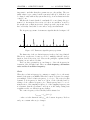
Unbunched beam longitudinal decomposition
Momentum spread
Due to spread in the momentum, ∆p, there is a spread in the synchrotron
frequencies, ∆f . From measuring the Schottky bandwidth of a harmonic
band, hence < ∆f >rms , the momentum spread can be calculated.
Intensity
The total amount of particles is proportional to the squared r.m.s. current
per band, i2rms∝ N . Every harmonic Schottky band has the r.m.s. current,
irms = 2efrev
be calculated.
N
2,
from which the amount of particles, the intensity, can
Figure 3.6: Unbunched Longitudinal Frequency Spectrum
3.3.3
Bunched beam longitudinal decomposition
From this signal we only measure the intensity, by measuring the values of
two harmonics according to the principle explained below. This section is
also introduces the effect of synchrotron oscillations on the spectrum even
though it isn’t used for parameter estimation.
Measuring intensity
The spectral components at harmonic frequencies, are in theory the same
for any harmonic, as mentioned before. However, this is not entirely true
in the real world. In section 3.2.1 the theory is derived for the transverse
pick-up, but the principle applies to the longitudinal as well. Say that only
two particles are detected and they have the same revolution frequency.
This is almost true for every particle, only they have different phases.
a(t) + a(t + ∆T ) ↔ A(f )(1 − ej(2π∆T f ) )
38
CHAPTER 3. SCHOTTKY NOISE
3.3. BEAM PARAMETERS
This is the effect that damps higher harmonics. We want to know only
the DC value from the longitudinal unbunched signal, but this band is not
fitted for measuring. In stead we measure at a frequency f and 2f . We
don’t know the ∆T , but from measuring two harmonic values we don’t need
to. Say we have two measurements, X1 and X2 and we want to find the
value A(f).
X1 = A(f )(1 − ej(2π∆T f ) ) = A(1 − K)
X2 = A(f )(1 − ej(2π∆T 2f ) ) = A(1 − K 2 )
Having these two equations with two parameters, we can eliminate K
and get an equation for the A, which is half the DC-value.
X12
2X1 + X2
Solving this equation will thus reveal the estimated DC value, without
measuring anything even close to this noisy band.
A=
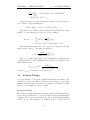
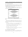
Fourier transforming the synchrotron oscillation
When the beam is bunched then the revolution frequency of each particle is
frev , in mean, but with an oscillation about this frequency. This is similar
to an equidistant distribution of pulses, but slightly sinusoidal displaced
in time. The same problem is known from signal processing as an inaccuracy/error in the moment of sampling. This is similar to a signal of the
nature, cos(anT + bsin(cnT + d)), which has the frequency spectrum shown
on figure 3.7
Figure 3.7: Complex of Synchrotron Satellites
The signal can be modulated as series of odd distributed delta functions.
i(t) = ef0
∞
δ(t − nT − τi sin(Ωs t + Ψi ))
n=−∞
39
CHAPTER 3. SCHOTTKY NOISE
3.3. BEAM PARAMETERS
by Fourier analysis this can be transformed into:
∞
i(t) = ef0 + ef0 Re[
exp(jnω0 (nT + τi sin(Ωs t + Ψi ))]
n=−∞
Using the relation exp(jzsinθ) = ∞
p=−∞ Jp (z)exp(jpθ), where Jp is
the Bessel function of first kind, the following equation is obtained.
i(t) = ef0 +ef0 Re[
∞
−j2πn f f
(e
∞
rev
n=−∞
J|p| (nω0 τi )exp(j(nω0 t+pΩs t+pΨi )))]
p=−∞
Taking only one single harmonic of this current:
f
in (t) = 2ef0 e−j2πn frev Re[
∞
J|p| (nω0 τi )exp(j(nω0 t + pΩs t + pΨi ))]
p=−∞
We see that this is just a frequency component, at nω0 t + pΩs , with an
f
amplitude of ef0 e−j2πn frev J|p| (nω0 τi ).
Every harmonic is a complex of several distributed frequency components, denoted satellites. Their amplitudes decreases significantly, with distance from the particles mean revolution frequency, p = 0, especially for low
harmonics. Already the first or second harmonic is almost zero, in the example showed below. The tail(hence frequency components for p = 1, 2, 3.)
gets longer with the harmonic number, n, whereas the centre component
gets smaller in a damped oscillating way (see fraction of Bessel function on
figure 3.8). One would think that, as the tails grew, the harmonics would
eventually overlap each other. But the distances between successive satellites is the synchrotron frequency, Ωs , and the distance between complexes
of satellites is the revolution frequency, ω0 . If the revolution frequency is
much larger than the synchrotron frequency, ωo >> Ωs , then this overlap
will be insignificant.
In a Matlab simulation the satellite complexes is obtained by creating
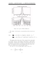
signals with a varying longitudinal displacement. It is seen from the plot,
figure 3.9, that the component at 1.65 [M Hz] is a bit larger than the one at
13.5 [M Hz], this is due to the overlap, from higher harmonics, mentioned
above. The synchrotron frequency used for this simulation is 0.15 [M Hz]
and the revolution frequency is 1.5 [M Hz]. Apart from this overlap, the
value corresponds to what must be expected, hence table 3.1.
In practical these Schottky spectra can not be measured. The signal
from a bunched longitudinal beam is too strong and the amplifiers can not
detect the fine differences between particles. In stead the amplitude values
of two harmonics are measured, one at, say m, and the other at 2m. By this
the DC value, of the beam, can be calculated. This is possible by knowing
the envelope function, which are derived in section 3.2.1.
40
CHAPTER 3. SCHOTTKY NOISE
3.3. BEAM PARAMETERS
Figure 3.8: Bessel function, Jp (nωi τi )
Table 3.1: Satellite amplitudes
Centre frequency
First satellite
Second satellite
Third satellite
J0 (2π
J1 (2π
J2 (2π
J3 (2π
0.1)
0.1)
0.1)
0.1)
< signal
< signal
< signal
< signal
>
>
>
>
0.9037*0.0269
0.2989*0.0269
0.0477*0.0269
0.0050*0.0269
0.0243
0.0080
0.0013
0.0001
Figure 3.9: Satellite generated from signal simulation in Matlab
The DC value is proportional to the number of particles in the beam.
In this mode the beam is decelerated, so the number of particles is surveyed
in case of loss.
41
CHAPTER 3. SCHOTTKY NOISE
3.3.4
3.3. BEAM PARAMETERS
Unbunched beam, transverse decomposition
Single particle
In the transverse plane, the particles are performing betatron oscillations
with a frequency of Qfi . The signals from a single particle detected by
a pick-up, can be simulated as, the betatron sine wave sampled with the
revolution frequency of the particle.
ii (t) = sinewave ∗ revolution = ai cos(2πfi qi t) ∗ δ(t − nTi )
Where ai is the amplitude of oscillations, Ti the time of revolution
and qi the fractional part of Q. The fractional part is used due to the
fact that the integer number of oscillations, in between discrete pick-ups,
can not be detected. For a single particle this is similar to a sine wave,
with a betatron frequency sampled with the revolution frequency. Thus a
frequency spectrum with lines of half the sine amplitude at harmonics, fi qi ,
frev − fi qi , frev + fi qi ,...Again simulated in the Matlab model, this reveals
a frequency spectrum as seen on figure 3.10.
Figure 3.10: Transverse Frequency Spectrum of Single Particle
In this case simulated with a revolution frequency of 1.51[M Hz] and a
betatron frequency of 50[kHz].
For N particles an analogy can be drawn to the calculations done on
the unbunched beam, in the longitudinal case. The theory was derived in
section 3.3.1 and the only difference is an introduction of an amplitude.
The amplitude is introduced as ai = arms + ∆ai and reduced as done with
the revolution frequency.
Here, as well, we get a spread in the frequencies and each
and every
band containing an r.m.s. current of, irms (fband ) = arms efrev N2 .
Several particles
When extending to many particles, we must take into account that the
particles have slightly different revolution and betatron frequencies. The
42
CHAPTER 3. SCHOTTKY NOISE
3.3. BEAM PARAMETERS
revolution frequencies of the particles are varying about the mean revolution frequency, between f0 ± 12 ∆f . The q values vary ∆qi about some mean
q and the resulting betatron frequency, for a given particle, is qi fi .
To illustrate how the spectrum looks like, when both fi and qi varies,
we let fi be constant and calculates the spectrum for a given interval of
q. Then repeating this, for several revolution frequencies, we can add our
spectra together and get an idea of how it looks like, for varying fi .
In the sketch, shown on figure 3.11, this is done with three constant
revolution frequencies. It is seen that in the cases of constant revolution,
we get spectra that looks as one would expect them to, hence single particle
spectrum shifted at each side of the revolution frequency. But the two
total harmonic spectra, consisting of the addition, has different Schottky
bandwidths. By comparing such adjacent Schottky bands, it is possible to
calculate ∆qi of a beam.
Figure 3.11: Example of different bandwidth of bands
The bandwidth of two adjacent Schottky bands are ∆f = (n ± q)∆fi ±
2πf0 ∆qi .
If it is possible to identify some identical patterns in both Schottky
bands, say a large peak or complex, then the q value can be determined
from either the peak or the complex. The q value for a peak would be
interpreted as being several particles having this (or close to this) betatron
oscillation frequency.
The estimated q value, for the betatron frequency, is the centre of a
complex of particle frequencies. This is the quantity calculated from the
unbunched transverse PSD spectra. The momentum spread is found from
other measurements, thus the frequency spread can be calculated and the
q value calculations can be corrected.
43
CHAPTER 3. SCHOTTKY NOISE
3.3. BEAM PARAMETERS
Emittance
Thus when each and every band contains the r.m.s. current,
irms (fband ) = arms efrev
N
2
, knowing frev and N enables calculation of arms . The signal from the
transverse pick-up is aimed to have a zero offset, so the mean value of a
beam passage, would be zero, < i(t) >= 0. For the emittance, 3, it is given
that the maximum amplitude, for a single particle, has the relation:
32σ =
4σ 2
β
So knowing the trajectory in the phaseplane for every particle enables
calculation of the total emittance. The maximum amplitude is not found
from the r.m.s. spectra, only the r.m.s. value of the amplitude. The
relation between the variance, of the amplitudes, σ 2 {a(n)}, and the r.m.s.
amplitude, arms , allowing negative a(n) s, is:
σ 2 {a(t)} =
=
∞
1 (a(n) − E{a(n)})2
N n=1
∞
1 a2 (n)
N n=1
= rms2 {a(n)}
= arms
So with a normal distribution of a(n) s, 2σ contains 95.5% of the amplitudes.
arms
β
√ L irms
= 4 2 √
ce N
32σ = 4
3.3.5
Bunched beam, transverse decomposition
The transverse pick-up senses both the transverse betatron oscillations and
the longitudinal displacement due to synchrotron oscillations. Thus there
is both the effect of oscillating signal amplitudes and an oscillating time
interval of passages. These two effects are combined in the equation.
44
CHAPTER 3. SCHOTTKY NOISE
di (t) = ai cos(qi ω0 t + φi )ef0 Re[
∞
3.4. PSD ESTIMATION
exp(jnω0 (t + τi sin(Ωs t + Ψi ))]
n=−∞
The last part is the same as for the longitudinal case only difference
here is a cosine wave multiplied by the expression already calculated in a
former section. In a frequency domain this is just a convolution between
a discrete frequency component of the cosine, at qi ω0 , of amplitude a2i and
the former obtained frequency spectrum. Again in a Matlab simulation,
this takes the form seen on figure 3.12:
Figure 3.12: Frequency spectrum of a bunched beam in the transverse plane
In this mode we calculate the same parameters as before, q and 3, when
the beam was unbunched. But as the particles are passing the pick-up, at
the same time, a common displacement from the closed orbit will result in
a great bias of the signal. This bias might saturate the amplifier so that
our signal information is lost. In such a case the system can measure the
parameters in a BTF4 mode in stead. This mode is described in section 3.7.
3.3.6
Parameter calculation summary
The seven parameters calculated by signal processing is summed up on
table 3.2, where f50% is the centre frequency of a Schottky band and n the
harmonic number.
3.4
PSD estimation
When we look at the power spectral density(PSD), of our signal, then it
looks something like the sketch at figure 3.13. Actually, there is a small
curvature of the noise floor, which is better estimated as a line with a
derivative. The calculations done in this section however assumes a straight
horizontal line, but this does not significantly effect the results obtained.
4
Beam Transfer Function
45
CHAPTER 3. SCHOTTKY NOISE
Quantity
Calc. from
N
irms
N
DC amplitude
< ∆p >rms
< ∆frev >rms
qV
f50%
qH
3V
f50%
irms
3H
irms
3.4. PSD ESTIMATION
Relation
<
2
N = e2i2 frms
2
rev
2|DC|2
N = e2 f 2
rev
rev >rms
∆p >rms = p<∆f
(nη<frev >)
q = <ff50%
rev >
q = <ff50%
√ revL>i
rms
√
32σ = 4 2 ce
√ Li N
32σ = 4 2 ce √rms
N
Beam State
Un./ Long.
Bu./ Long.
Un./ Long.
Bu.+ Un./Trans.
Bu.+ Un./Trans.
Un./Trans.
Un./Trans.
Table 3.2: Parameters calculated
The power spectral density estimate is found from Fourier transforming
the detected signal and then multiplying with a constant according to the
equation:
2fs
|X̂(k)|2
N
And the estimated power in a band, is just an addition of the estimated
power spectral density components in this very band.
Ĝ(k) =
Schottky Noise
K
Noise floor
Figure 3.13: PSD of Schottky Noise Signal and Noise Floor
Schottky noise distribution
We define the signal to noise ratio to be calculated in a band, bounded
by ±2σ. This is two standard deviations, which contains 95.45% of the
Schottky signal. This is sketched on the figure as vertical punctured lines.
46
CHAPTER 3. SCHOTTKY NOISE
3.4. PSD ESTIMATION
The signal to noise ratio is the ratio of the two areas between the vertical
lines. For these calculations we freeze the Schottky distribution and vary
the power of the noise floor level with the SNR.
SN R =
0.9545
µN oisef loor
Each PSD component of the Schottky noise, has a statistical variation
about the theoretical distribution. We assume that each component is right
in mean, but with a standard deviation of a certain percentage, k. Each
component is then distributed as.
P ∈ N (µSchottky , kµSchottky )
- and the mean values for all of these components vary with the Schottky
distribution after the formula.
1 x−µ 2
1
PGaussian = √ e− 2 ( σ )
σ 2π
This function can not be analytically integrated. Numerically it is found
that the integral between −σ and +σ is 0.9545. The integral of the squared
function in the same interval sums up to 0.2808.
We only have discrete values of this function because the frequency
interval is always split up in 256 or 512, depending on the FFT length. So
we have a finite array of constants which corresponds to the distribution of
the mean values.
The sum of the Schottky power spectral density components with different distributions can be rewritten to be a sum of equally distributed
components. The rule for a normal distributed variable multiplied with a
constant is.
X ∈ N (1, σ) ⇒ cX ∈ N (c, cσ)
Psum = x1 + x2 + ... + xN
= c1 x + c2 x + ...cN x
M
∈ N(
i=1
M
∈ N(
µSchottky,i
M
, σ2
M
ci , k c2i )
i=1
i=1
47
Schottky,i )
i=1
CHAPTER 3. SCHOTTKY NOISE
3.4. PSD ESTIMATION
Noise floor distribution
The noise floor is rectangular distributed in frequency, as sketched on figure 3.13. The spectral components are then in mean equal to this value
and we presume that the standard deviation is proportional to this by a
factor, h. The power spectral density components are distributed as:
P ∈ N (µN oisef loor , hµN oisef loor )
Noise floor estimation
We would like to estimate this noise floor, to be able to subtract it from our
Schottky band power estimation. We do this by taking a lot of samples,
N , of only the noise floor. By doing this we can estimate the mean noise
floor power, µN oisef loor , with a variance of
2
σN
oisef loor
N
Then we can subtract the estimated noise floor power from the total
measured power.
2
σN
oisef loorestimate =
Pmeasured = PSchottkynoise + PN oisef loor − P̂N oisef loor
We allmost never get an exact estimate of the noise floor. If we want to
make an analysis, of the noise floor estimate, that holds for 95.45% of the
cases, then we need to consider a standard deviation of 2σ. So the noise
floor contribution, when subtracted the offset, is set to be:
h0.9545
hµN oisef loor
√
√
=2
N
SN R N
This error is added every Schottky spectral component, so it is important to minimise this contribution. We set this to the maximum, in order
to perform a worst case analysis. Then we know that 95.45% of the cases
are better than estimated, thus rarely worse.
3N oisef loor ≤ 2σ̂N oisef loor = 2
Total measured signal
The signal measured is then both Schottky noise and compensated noise
floor.
Pmeasured ∈ N (M 2
M
h0.9545
√ +
SN R N i=1
M
0.95452
2
ci , M h2
+
k
c2i )
2
SN R
i=1
From this it is clear that our estimate, of the Schottky band power ,is
almost always biased. There are three parameters which can make this
48
CHAPTER 3. SCHOTTKY NOISE
3.4. PSD ESTIMATION
bias less significant. First of all we need a large signal to noise ratio, which
is the best way to cope with the problem. Another way is to begin the
accumulation of samples as close to the Schottky band as possible, thus
minimising M . The last method is to estimate the noise floor with as
many samples as possible, raising N .
Estimate inaccuracy
How much is estimate biased and how significant is the standard deviation
of the estimate ? The two quantities tells us how reliable the estimated
power of the Schottky band is.
3bias =
=
=
3σ =
bias
µScottky−power
h0.9545
√
M 2 SN
R N
M
i=1 ci
2M h
√
SN R N
σScottky−power
µScottky−power
=
k2
=
M
2
2 0.95452
i=1 ci + M h SN R2
M
i=1 ci
k2 0.2808 +
M h2 0.95452
SN R2
0.9545
Examples
If we set the Schottky noise and noise floor standard deviation to be 10%
of the mean value, then this is equal to h = k = 0.1. The sample lengths
are set to respectively 256 and 512, M = 256 or M = 512, and we measure
the noise floor from 4096 samples, N = 4096. The signal noise ratio set to
either 10 or 100. This reveals.
3bias (SN R = 10, size(F F T ) = 256) = 0.080
3bias (SN R = 1000, size(F F T ) = 256) = 0.001
3bias (SN R = 10, size(F F T ) = 512) = 0.160
3bias (SN R = 1000, size(F F T ) = 512) = 0.002
3σ
(SN R = 10, size(F F T ) = 256) = 0.169
3σ
(SN R = 1000, size(F F T ) = 256) = 0.055
3σ
(SN R = 10, size(F F T ) = 512) = 0.233
49
CHAPTER 3. SCHOTTKY NOISE
3σ
3.5. EFFECT OF WINDOWING
(SN R = 1000, size(F F T ) = 512) = 0.055
From this is seen that if our signal to noise ratio is not significantly
high, then we can’t rely on the result. The bias error can be improved by
taking more samples of the noise floor, whereas the standard deviation is
unaffected by this.
It should be kept in mind that this analysis is theoretical and only
describes the mechanisms, the numbers are thus not estimates of real errors.
Estimates of real errors requires knowledge of real parameters and these are
not known at the moment. They can only be found by statistical studies of
the AD beam nature. The analysis made is however fully applicable, when
it comes to deciding the importance of the different parameters.
3.5
Effect of Windowing
All of the above calculations are carried out on ideal signals, unaffected by
the processing that the signals are submitted to. However the signals are
NOT ideally transformed into their frequency spectra. First of all, the FFT
algorithm presumes that the signal is periodic, with the FFT length. If this
is the case, then the algorithm is precise. The assumption implicitly made
by the FFT algorithm is sketched in figure 3.14. The solid line represents
the real input data and the dashed line the extrapolation assumed by the
algorithm.
time
Figure 3.14: Signal assumed by the FFT algorithm
For a Schottky noise signal this assumption is wrong. There is no such
periodicity. When there is not a periodicity, there will be a ”discontinuity”5
in the assumed signal input. This induces frequency components that are
not present in the signal, but originates from the abrupt transition from
one end to the other.
To avoid this abrupt change, we can multiply with an envelope function
that declines towards zero, near the ends of the signal input vector. Such a
5
Discontinuity is put in quotation marks because a discrete signal, by definition,
always is discontinuous, but not necessarily with these large jumps of subsequent signal
values
50
CHAPTER 3. SCHOTTKY NOISE
3.5. EFFECT OF WINDOWING
function is denoted a window function and is normally used when Fourier
transforming a discrete signal.
On figure 3.15 the difference between windowed and non-windowed
Fourier transformations, is shown. Note that the windowed versions get
smeared a little, but not significantly, whereas the non-windowed is either
precise or quite smeared.
Figure 3.15: Consequence of windowing before performing FFT
Different window functions
A straight-forward window function, is the rectangular window which has
the spectrum.
Hsquare (f ) = a
sin(πf N ∆T ) −jπf (N −1)∆T
e
sin(πf ∆T )
This frequency spectrum has a good mainlobe, in fact the best we can
get from the chosen number of coefficients. The sidelobes, however, are
quite wide this is the price we pay to cut off the signal so sudden. We can
however do it softer, by using other window functions such as Hamming,
Hanning, Blackman, Bartlett or even a home constructed one. These have
frequency spectra with less significant side lobes but wider main lobes (see
figure 3.16). At figure 3.15 a Hanning function was used
51
CHAPTER 3. SCHOTTKY NOISE
3.5. EFFECT OF WINDOWING
The analogue spectrum of these, above mentioned window functions,
can be calculated by use of the spectrum of the rectangular window function, in combination with the rule of frequency shifting.
ejω0 n x[n] ↔ X(ej(ω−ω0 ) )
The Hamming (a = 0.54 b = 0.46) and Hanning (a = 0.50 b = 0.50)
window are easily calculated as.
ω(M +1)
H(f ) =
ωM sin(
2
ae−j 2
sin( ω
)
2
)
(ω− 2π )(M +1)
M
(ω− 2π )M sin(
)
b
M
2
2
− e−j
2π
(ω− )
2
sin( 2M )
(ω+ 2π )(M +1)
M
)M sin(
)
b −j (ω+ 2π
M
2
2
− e
(ω+ 2π
)
2
sin( 2M )
The rectangular Hamming and Hanning window spectra, are drawn at
figure 3.16. At the dB scale, looking at the side lobes, the rectangular
window is the largest, then the Hamming and at last the Hanning. The
window chosen for this application is Hanning because the side lobes, close
to the mainlobe, is damped the most.
The effects of windowing is smearing of the true signal spectrum because of the convolution with the window spectrum. This has two effects,
first two distinct frequencies can merge, if they are closely placed to one
another (loss of resolution) and second a single frequency is affected by
sidelobes from the surrounding frequencies (leakage).
Overlap
By using a window function we sort of throw away some data, when we
weight the signal vector values near the ends very low. To use the data
better, we perform Fourier transformation by overlapping signal input vectors. This enables us to analyse all of the data vector values almost equally,
but still without introducing artifacts from abrupt ”signal-discontinuities”.
We use 50% overlap, which is the maximum overlap without introducing
redundant information.
PSD compensation from windowing
When the power spectral density values are calculated, we square the calculated Fourier transformed components.
Ĝ(k) =
2fs
|X̂(k)|2
N
52
CHAPTER 3. SCHOTTKY NOISE
3.5. EFFECT OF WINDOWING
Figure 3.16: Spectra of Window Functions
The estimate of the frequency components has an effect from the windowing.
Ĝ(k) =
=
2fs
|... + H(−1)X(k + 1) + H(0)X(k) + H(1)X(k − 1) + ...|2
N
2fs
(... + H(−1)2 |X(k + 1)|2 + H(0)2 |X(k)|2 + H(1)2 X(k − 1)|2 + ...)
N
The squaring of the absolute sum of X(k) contains absolute values which
are correlated. However, the frequency components are complex with a
random phase. Carrying out the calculation of the absolute value written in
the first line, reveals products of real values from different Fourier spectra.
These, as well as the product from the imaginary parts, has a mean of zero.
The only contribution left comes from squared values.
The total power of the Schottky signal is a sum of all powers.
P̂total =
N
k=1
P̂ (k) = ∆f
N
Ĝ(k)
k=1
53
CHAPTER 3. SCHOTTKY NOISE
=
3.6. ANALYSIS TIMING
N
2h
(... + H 2 (−1)|X(k + 1)|2 + H 2 (0)|X(k)|2
∆f
N
n=1
+H 2 (1)|X(k − 1)|2 + ...)
A single frequency component appears several places in the expression
above. In all a component sums up to.
P̂ (k) = X(k)(... + H 2 (−1) + H 2 (0) + H 2 (1) + ...)
From this is seen that the window function is attenuating the input
signal, so a compensation factor is needed for the estimate.
KHanning =
∞
H 2 (k) =
n=−∞
N
1 h2 (n)
N n=1
= 0.3765(N = 256) or 0.3757324(N = 512)
This is thus the attenuation for every component, compared to the ideal
squared sum we have to compensate for this factor.
P̂total =
N
2h∆f
X 2 (k)
N KHanning n=1
This is for a single input signal. Performing Fourier transformations
of signals with x% overlap i slightly different. By this we weight the total
signal with the factor.
KHanning (x, M ) =
0.40Naverages
(Naverages + 1)(1 − x)
- where Naverages is the number of averages done.
3.6
Analysis Timing
Now we should have covered most of signal nature and the uncertainty of the
calculations of its power. This section is sort of the interface between this
unlimited signal frequency spectrum, to the limited bandwidth processing.
It is serves as a transition to the processing.
Transverse timing
The transverse signal timing is the most important. With this signal there
is a spectral zoom that has to be performed whereas the longitudinal signal
treatment only needs to know the harmonic. The longitudinal signal timing,
is thus left out. The transverse is explained in more details, but it is
54
CHAPTER 3. SCHOTTKY NOISE
3.6. ANALYSIS TIMING
important to underline that these parameters are only guiding. They are
initial values for processing, but the system is build up so that these can
be changed easily without any system knowledge, from workstations in the
control room.
Whether the beam is bunched or unbunched does not change the spectrum a lot. As mentioned in section 3.3.5 there are satellites, created by
the synchrotron oscillations, in stead of single spectral components. As we
have a Schottky band, this does not affect our spectra that much.
The frequency spectrum of a transverse signal is sketched at figure 3.17
frev
2frev
3frev
4frev
Figure 3.17: Transverse signal frequency spectrum
The harmonics of the revolution frequency is showed as being identical.
This is not exactly true because we need to multiply with the envelope
function, derived in section 3.2.1. However the principles, explained in the
following, are not affected by this.
There are three parameters we can change to derive the frequency information of the Schottky band. These are clock frequency, decimation
ratio and local oscillator frequency.
Clock
When the revolution frequency is constant, we sample close to the maximum clock frequency, at 40MHz. When the beam is decelerated, we sample
at a multiple of the revolution frequency, fs = ki frev . The reason for this
dynamic clock frequency is, that we zoom in on the Schottky band by
setting a local oscillator frequency, fLO . This frequency has to be a constant fraction of the sampling frequency. So if the sampling frequency was
not dynamic, then the spectrum zoomed upon, would change during data
acquisition as the revolution frequency changes.
The centre frequency of the Schottky band is situated at
fSchottky = frev (m ± q)
- where m is the harmonic and qfrev the betatron frequency. Both m
and q are constant whereas frev changes.
55
CHAPTER 3. SCHOTTKY NOISE
3.6. ANALYSIS TIMING
fSchottky
fLO
frev
m±q
=
= (m ± q)
=
fs
fs
fs
ki
From the equation above, it is seen that the LO frequency can be set
by only combining m,q and ki .
The original anti-aliasing filter of the Pentek 6441 ADC has a pass band
and stopband frequency of respectively 16 and 24 MHz. This is too high
for our application, as we need to lower the sampling frequency more than
this filter alowes. In stead another one, with a passband and stopband
frequency of respectively 8 and 15 MHz, is added. The signal is damped
more than 40 dB beyond this stopband frequency.
If we only alowe 40 dB damped image frequencies in the baseband and
our baseband is set from DC to 7 MHz, then we have a minimal Nyquist
frequency of, 7 + 15−7
2 = 11 M Hz. So we can sample our signal with clock
frequency down to 22 MHz.
Decimation Ratio
The decimation ratio reduces the bandwidth, thus enabling fast calculation
of the signal Fourier transformation, see section 4.3 for details. We still need
to have sufficient bandwidth, to look for our Schottky band, so we restrict
this bandwidth to be 11.25% of the revolution frequency, BW
frev = 0.1125.
Unfortunately this bandwidth is affected by ripple in the passband. This
ripple comes from the low pass filtering in the DRX after down mixing. The
ripple becomes more significant when we approach the passband frequency.
To avoid too much ripple, we only use 60% of the low pass bandwidth.
This bandwidth is guaranteed to have less than ±0.04 dB of ripple. We still
perform an FFT of all the samples, but reject 40% when the transformation
is done. This is equal to rejecting the samples from 0.3fN to 0.7fN . This
rather art interval in the middle of the spectrum, is because the positive
frequencies of the spectrum lies between 0 and 0.5fN and the negative from
0.5fN and fN . With a complex signal these negative frequencies are NOT
necessarily images of the positive.
This ratio is derived beneath.
fN =
ki fs
fs
=
4R
4R
BW
= 0.6fN
frev
ki
BW
= 0.6
frev
4R
56
CHAPTER 3. SCHOTTKY NOISE
3.6. ANALYSIS TIMING
Local oscillating frequency
The LO frequency is set to a presumed value of the Schottky band centre
frequency. The value has to be in the frequency interval, where the head
amplifiers have low noise, between 5.5 and 6.5 MHz. This area is shaded
on the sketch at figure 3.18. It corresponds to the revolution frequency of
1.5 MHz and a q value of 0.4, which are realistic, values when the beam is
injected.
frev
2frev
3frev
4frev
Figure 3.18: Transverse signal frequency spectrum
From this, it is seen, that we have to make a zoom upon the 4th harmonics lower Schottky band, for short 4minus . This has a frequency of
(4 − 0.4) ∗ frev = 5.4 M Hz. This value is sent to the DRX, as a fraction of
the sampling frequency. It is sent as 32 bit number, so the actual number
sent would be:
5.4 M Hz 33
2 = 1.159.641.17010 = 451EB852h
40 M Hz
The real q value should lie within ±5.5% of this guess. The q value is
distinguished with steps of
∆q =
0.1875
0.1125
=
0.6Nf f t
Nf f t
This resolution we set to be greater than 1e-3, q ≥ 1e − 3.
Constraints
We can sum up these constraints into five rules.
• The maximum sampling frequency can’t be exceeded, fs ≤ 40 M Hz
• To avoid image frequencies in baseband we can not have a sampling
frequency lower than, fs ≥ 22 M Hz
• The head amplifiers have the required low noise characteristics only
in a limited band between 5.5 M Hz and 6.5 M Hz.
• The bandwidth-revolution-frequency ratio,
57
BW
frev ,
is set to be 11.25%.
CHAPTER 3. SCHOTTKY NOISE
3.6. ANALYSIS TIMING
• The step in q is set to be not higher than ∆q ≥ 1e − 3
3.6.1
Parameters calculated in EXCEL sheet
The constraints mentioned above are obeyed in the EXCEL sheet shown
on figure 3.19. The sheet calculates the key parameters needed, to do the
digital downmixing and signal processing of the Schottky signal. Around
the key parameters there are a bunch of other numbers of greater or minor
interest. To get an overview of these central calculations the sheet is gone
through in this section.
At the first column, we see the only given parameter for this sheet,
the variation of the momentum, p. This momentum is linear between the
two columns, ”p from” and ”p to”. Each row is a time-slice in which all
hardware and software settings are constant. In a popular sense, this can
be thought of as a ”car-gear” that doesn’t need to be changed, even though
the speed changes a little bit. In our system this means that neither the
setup of the DRX nor the FFT parameters changes during this time, even
though the sample frequency changes a little. The duration of the time slice
is depended on the amplifiers. The zoom has to be done within a specified
range restricted by the amplifier characteristics.
The different states of the beam are divided by shaded horizontal bars.
For the Schottky measurement there are only two important states, these
are when the beam has a constant revolution frequency, hence constant momentum, or varying revolution frequency. The different momentum levels
are graphically shown in time on figure 2.9 on page 28.
In the EXCEL sheet there are some vertical columns shaded light gray,
these are the key parameters from which almost all the other columns are
derived. There are however columns concerning the fast Fourier transformation, which are decided independently.
As appendix on Appendix A all of the column names are explained and
possibly added a formula for the calculation of the column. The information
should be complete, thus reproduction of the Excel sheet can be done from
this.
58
alfa = 0.6
q = 0.4
Figure 3.19: Measurement state data
Transverse sample clock and Schottky band harmonics
q
Ki, R,
Decimation bandwidt Schottky band
harmonic,
factor
h
q resolution constant
Momentum
Revolution frequency
Sampling Frequency
chosen
Local oscillator frequency
time of measurement
Sampling rates
Angle of envelope
START:
angle of END: angle
exp.funct. of exp.funct.
meas.ti
total
Complex Complex envolope at envolope at
f_s/2
f_s/2
p from p to f_rev from f_rev to K_i f_s from f_s to
R
BW/f_rev harmonic sign of q LO from LO to F/2^32 N_av N_FFT me* # of meas. delta_q/BIN period sample rate sample rate
[degrees] [degrees]
(GeV/c) (GeV/c) (MHz)
(MHz) (integer) (MHz)
(MHz)
(integer)
()
(integer)
()
(MHz) (MHz)
()
()
( ) (msec)
()
( in 1e-3 ) (msec) (highest)
(lowest)
constant:
1.590
1.590
20000
3.592 3.592
1.590
1.590
40.000 40.000
32 0.1179
4 minus
5.724
0.143 16
512 13.9
1436
0.38
20000
312500
312500
6.84
8.09
decel. to
1.590
1.590
3500
3.592 2.359
1.590
1.527
15 23.850 22.905
20 0.1125
4 minus
5.724 5.497 0.240 16
512 15.2
178
0.37
2714
298125
286313
6.84
8.09
2.359 2.001
1.527
1.488
15 22.905 22.320
20 0.1125
4 plus
6.719 6.547 0.293 16
512 15.6
50
0.37
786
286313
279000
7.12
8.42
constant:
1.488
1.488
228
15000
2.001 2.001
1.488
1.488
40.000 40.000
36 0.1120
4 plus
6.547
0.164 16
512 15.7
957
0.36
15000
277778
277778
7.31
8.64
decel. to
1.488
1.488
3500
2.001 1.099
1.488
1.250
24 35.712 30.000
32 0.1125
4 plus
6.547 5.500 0.183 16
512 18.6
99
0.37
1856
279000
234375
7.31
8.64
1.099 0.741
1.250
1.019
27 33.750 27.513
36 0.1125
5 plus
6.750 5.503 0.200
8
512 12.1
61
0.37
736
234375
191063
8.70
10.29
0.741 0.575
1.019
0.859
27 27.513 23.193
36 0.1125
6 plus
6.522 5.498 0.237
8
512 14.3
23
0.37
342
191063
161063
10.68
12.62
0.575 0.475
0.859
0.743
42 36.078 31.206
56 0.1125
7 plus
6.357 5.498 0.176
8
512 16.5
12
0.37
205
161063
139313
12.66
14.97
0.475 0.397
0.743
0.640
42 31.206 26.880
56 0.1125
9 minus
6.390 5.504 0.205
8
512 19.2
8
0.37
162
139313
120000
14.64
17.30
0.397 0.318
0.640
0.528
42 26.880 22.176
56 0.1125
10 plus
6.656 5.491 0.248
6
512 18.1
8
0.37
161
120000
99000
17.00
20.09
0.318 0.300
0.528
0.501
45 23.760 22.545
60 0.1125
12 minus
6.125 5.812 0.258
6
512 19.1
1
0.37
37
99000
93938
20.60
24.35
constant:
0.501
0.501
212
6000
0.300 0.300
0.501
0.501
40.000 40.000
104 0.1152
12 minus
5.812
0.145 16
512 45.3
132
0.37
6000
96154
96154
21.71
25.66
decel. to
0.501
0.501
2000
0.300 0.259
0.501
0.437
78 39.078 34.086
104 0.1125
13 minus
6.313 5.506 0.162 12
256 20.3
20
0.73
414
93938
81938
21.71
25.66
0.259 0.221
0.437
0.377
78 34.086 29.406
104 0.1125
15 minus
6.380 5.504 0.187 10
256 19.9
18
0.73
376
81938
70688
24.90
29.42
0.221 0.193
0.377
0.331
78 29.406 25.818
104 0.1125
17 minus
6.258 5.495 0.213
8
256 18.6
15
0.73
281
70688
62063
28.86
34.10
0.193 0.165
0.331
0.284
78 25.818 22.152
104 0.1125
19 plus
6.421 5.510 0.249
8
256 21.6
13
0.73
283
62063
53250
32.87
38.84
0.165 0.140
0.284
0.243
87 24.708 21.141
116 0.1125
23 minus
6.418 5.492 0.260
8
256 25.3
9
0.73
243
53250
45563
38.31
45.27
0.140 0.119
0.243
0.207
108 26.244 22.356
144 0.1125
27 minus
6.464 5.506 0.246
8
256 29.7
7
0.73
211
45563
38813
44.77
52.91
0.119 0.100
0.207
0.174
129 26.703 22.446
172 0.1125
31 plus
6.500 5.464 0.243
8
256 35.3
5
0.73
192
38813
32625
52.56
62.11
constant:
0.174
0.174
87
1000
0.100 0.100
0.174
0.174
40.000 40.000
306 0.1127
34 plus
5.986
0.150
1
256
7.8
128
0.73
1000
32680
32680
62.52
73.89
onstants:
59
3.6. ANALYSIS TIMING
CHAPTER 3. SCHOTTKY NOISE
CHAPTER 3. SCHOTTKY 3.7.
NOISE
BEAM TRANSFER FUNCTION(BTF)
3.7
Beam transfer function(BTF)
Our aim of processing is to be able to analyse the Schottky noise signals.
However it might happen, that these signals are too weak for analysis. In
such a case there is another possibility for tune measurement, namely the
beam transfer function calculation. This is an older and simpler method of
measuring. The method is only mentioned here, as the report has its main
focus on the Schottky signal processing.
Calculation of the beam transfer function, involves disturbance of the
beam. Basically, the beam is kicked a little bit and the response is measured
by the pick-ups. What happens physically is that the oscillations becomes
larger and thereby the pick-up signals as well. The snapshot of the beam
on figure 2.7 is at the time of kick displaced vertically. Each particle is still
moving around the origin, the shape changes to a ”snail-like” trajectory
around the origin. As the area, also known as the normalised emittance,
stays the same, the fundamental theorem of Louville still holds.
The calculation of the BTF simply has to signal inputs, the kicker signal
and the detected beam signal. These are Fourier transformed and the ratio
between them are found.
BT F (f ) =
Detected(f )
Kicked(f )
60
Chapter 4
Hardware
This section begins with an overall description of the designed system at
block level. Each an every block is shortly introduced and the functionality
in the system mentioned. Blocks, such as the ADC and DRX boards are
described slightly more detailed than the others. More profound descriptions follows in the sections describing the downconverter and the digital
signal processor chip. A range of features is introduced in order to prepare
the reader for the later sections describing the written software, using these
features.
4.1
Overall system description
The control of a synchrotron is a delicate matter. First of all there is a
great need of accuracy and secondly it has to happen at a very specific
time. Some tasks has to be controlled down to 1 millisecond, so timing
is an important parameter. The system, to be controlled, is shown on
figure 1.3 on page 12. Note that building are situated in the middle of the
PS synchrotron, so that there is the same signal delay to all cells of the
lattice. Underlining the importance of high accuracy timing. The AD is
situated to the left, as a rectangular building at the left with an oval-like
lattice inside.
The AD control system, of which the embedded Schottky analysis system is connected to, is quite large. There are a lot of blocks that works in
parallel controlled by central control units, the device stub controllers(DSCs).
A block diagram is shown on figure 4.1. The description is first divided into
the blocks, shown on the figure and later the measurement procedure of the
system, as a whole, is described.
61
CHAPTER 4. HARDWARE 4.1. OVERALL SYSTEM DESCRIPTION
Texas Emulator / Debugger / Cross-compiler
23
Fixed
2x
Variable
DDS
f_rev
DAU
ClkGen
23
PC
40 MHz
K
f.meas.
PU
12/14
12/14
J-Tag
6510
6441
Kicker
Longitudinal
DRX
PU
ADC
Horizontal
12/14
12/14
16
J-Tag
16
4270/
4269/
4257
16
DSP
Vertical
6441
ADC
Clock
PU
16
Vertical
Kicker
Horizontal
Timing
TG8
Dig. I/O
Dig. I/O
VMEbus
DSC
WS
WS
WS
Ethernet
Figure 4.1: Block diagram of acquisition and processing system
4.1.1
Description of blocks
Pick-ups(PU) and amplifiers
There are three pick-ups made, for the beam detection. A transverse horizontal, a transverse vertical and a longitudinal pick-up. The induced currents on the pick-ups surfaces are quite weak and they are amplified by
head amplifiers sitting on the pick-ups them selves. These amplifiers are a
delicate matter. The noise contribution of these are made as low as possible. The head
√ amplifiers on transverse pick-ups has a noise level between
0.3 − 0.5 pA/ Hz in frequency interval between 5.5 − 6.5M Hz. The longitudinal signal analysis needs a larger bandwidth, so three amplifier
√ gain
modes √
are used. The power spectral density noise is either 1.6 pA/ Hz or
15 pA/ Hz depending on the gain mode.
After the head amplifiers, there is another amplifier/attenuator. It is
controlled by software, in order to use the maximum dynamic range of the
ADC. The amplifier/attenuator has a gain from -17 to +28 dB in 16 steps.
4 bit codes the amplification level, so the LSB is equal to 28−−17
24 −1 = 3dB.
The amplifier also has an anti-aliasing filter, which matches the requirements of the quantisation. Two filters are present, the existing Pentek
anti-aliasing filter and the added filter having lower bandpass characteristics. The switching to and from the additional filter is under software
control.
62
CHAPTER 4. HARDWARE 4.1. OVERALL SYSTEM DESCRIPTION
Timing Module(TG8)
For the system timing, a CERN TG8 timing module is used. This module
has 8 output channels and can receive an input request of an interrupt via
the VME bus.
Digital Arithmetic Unit(DAU)
As incoming signal to our system, we have the revolution frequency represented in 23 bits. This frequency has to be multiplied by the ki factor
to obtain the sampling frequency information. This DAU carries out this
multiplication.
Direct Digital synthesiser(DDS)
A DDS module converts the sampling frequency information into a train
of pulses at half the sampling frequency. The module can only generate a
pulse train of maximum 20 MHz.
Doubler (2x)
As we need a pulse train at a maximum frequency of 40 MHz, we need to
double the the frequency and this is done by a doubler module.
Fixed clock
A fixed digital pulse train of 40 MHz is produced by a crystal oscillator
module.
Digital I/O
The digital I/O modules serve as interface of data from the VMEbus to
modules not attached to this bus.
Pentek 6441 Analog to Digital Converter(ADC)
Figure 4.2: VME crate embedded Pentek 6441 ADC card
As converter we use a an VME crate embedded Pentek 6441 analog to
digital converter which quantifies in 12 bits at 40 MHz. The specifications
for this ADC is written in appendix B. They are directly taken from the
63
CHAPTER 4. HARDWARE 4.1. OVERALL SYSTEM DESCRIPTION
manual, which is currently1 available on the Internet at [19]. The card is
shown on figure 4.2
The internal block diagram of the ADC is shown at figure 4.3
Figure 4.3: Block diagram the ADC
Pentek Digital Receiver 6510 (DRX)
Figure 4.4: VME crate embedded PENTEK 6510 digital receiver card
As receiver of the digitized signal the Pentek 6510 Multiband Digital
Receiver MIX module is used, see card on figure 4.4. The digitised data is
received at a sample rate of up to 40 [M Hz]. The data is reduced in the
receiver to minimise the calculation load for the subsequent real time FFT
analysis. The specifications are written in appendix C.
With the digital mixer, the interesting frequency band is down converted to a band at low frequencies. This band is lowpass filtered and
decimated. The principle is that the band of interest, at first, takes up
very little of the whole band. Thus making a zoom by just removing all
other frequency information leaves you with very few samples. Then details
can be inspected after a subsequent Fourier transformation of the reduced
data. The principle is described in section 5.2.1 on page 84.
At the board there is as well a Texas Instruments DSP, TMS320C40.
This is a central component for this project and will be discussed a lot more
1
September 1998
64
CHAPTER 4. HARDWARE 4.1. OVERALL SYSTEM DESCRIPTION
profound later in this report, see section 4.4.
Similar to the ADC there is, at the moment, available manuals and
specifications for the 6510 DRX on the WEB at [19].
Figure 4.5: Block diagram of Digital Receiver
Digital Signal Processor (DSP)
The digital signal processor board on the block diagram is not included
in the current system version. This is an option for further development,
when the cheaper version has shown its worth. This is why the board is
shown with punctured lines.
65
CHAPTER 4. HARDWARE
4.2. MEASUREMENT PROCEDURE
A version with DSP board will include a board with multiple processors.
The boards considered was the Pentek 4269, 4270 and 4257 DSP boards all
with either 2 or 4 TMS320C40’s. Information about these boards can be
found at [19].
Device Stub Controller (DSC)
The backbone of the control system is the Device Stub Controller, DCS.
The DSC has a CES RI08062 CPU (PowerPC) and are embedded in VME
crates. There are more than 100 of these DSCs in the PS complex. The
DCS controls every device attached to the common bus, in terms of requests, timing, handshaking, addressing etc. The operating system of this
DSC is LynxOS 2.5. It is a unix based real-time operating system. As
all other real-time operating systems, LynxOS works on an interrupt basis,
with interrupt rates down to 5 milliseconds
The DSC is connected to Ethernet through an interface. It is also
connected to a VME bus. The VME bus system is a 160 PIN bus connection
with a transfer rate of 160 M byte/sec.
Work stations(WSs)
The workstation in the PS network are unix based terminals and PCs.
The workstations have IBM RS/6000 CPUs and they’re using the Unix
AIX operating systems, which is the IBM made unix system. The PCs are
using Windows 95/NICE and are communicating with the control system
via an X-console. They are both connected to Ethernet, which runs the
communication protocol TCP/IP2 .
4.2
Measurement procedure
All parameters of the measurements are controlled by work stations. They
give a measurement request to the device stub controller, DSC, via Ethernet. This request contains data of everything concerning system measurement setup. When data is received by the DSC, it takes full control of
the measurement. Time interrupts are requested of the TG8 and all of the
system is set up via the VME bus. The following things are set up before
the data acquisition can begin.
• levels of signal amplification, -17 - +28 dB
• choice of measurement, Schottky or BTF
• choice of clock source, fixed or variable
2
Transfer Control Protocol/Internet Protocol
66
CHAPTER 4. HARDWARE
4.3. HARRIS HSP50016 DRX CHIP
• setup of variable clock factor, K
• setup of DRX, 8 control words of 40 bits to each receiver chip
• setup of DRX data buffer
• setup of a DSP processing request
When the requested time interrupt occurs, the DRX buffers are enabled
thus collecting downsamled data for processing. When the buffers are half
full, they interrupt the DSP so that the DSP can empty data buffer and process data. When a sufficient number of data is collected, the DSP disables
the data buffer of the DRX. When the DSP has finished the calculations
on data, the DSC is informed. The DSC can then take the calculated data,
from global shared memory, and deliver it to work stations, where it is
presented.
This is the main lines of the overall procedure. The specific internal
publication defining this, is not finished at the time of the writing of this
report. The structure is however clear and the software modules are written, so that they can be changed whenever the final specifications are ready.
An early draft of the publication is made by the writer of this report, but
it needs modifications and approval of a system aquianted. The definitions
are bound to be ready towards the end of this year, 1998.
4.3
Harris HSP50016 DRX chip
Figure 4.6: The Harris HSP50016 downconverter chip
The HSP50016 Harris downconverter chip basically only has two important features. The down conversion to baseband and reduction of bandwidth. This is the same as watching the signal spectrum through a window
of optional width, at an optional spot. The frequency spectrum range, goes
up to 75 MHz and in this range the chip can produce output with a bandwidth of between ∼ 600 Hz to ∼ 1.2 MHz. At the maximum data rate, the
baseband for down conversion can be set at 0.01 Hz of precision.
67
CHAPTER 4. HARDWARE
4.3. HARRIS HSP50016 DRX CHIP
The down-converter chip is the fastest component in the system developed. The Pentek 6510 Digital Receiver contain 8 of those 48 pin digital
down converter chips. This is what enables us to perform spectral analysis, at such data acquisition rates, hence we acquire close to 2 GSPS3 .
The digital receiver, also denoted DRX, can acquire and process 16 bit of
input data in up to 75 MHz, thus a possible data rate of 1.2 GSPS4 per
chip. This is not possible to process with any existing DSP, so without the
down-mixing this spectral analysis could not meet the real time constraints.
What the Harris chip is doing is basically shown on figure 4.7. The
principle of downmixing is explained in section 5.2
Figure 4.7: Simple internal block diagram of the Harris chip
4.3.1
DRX functionality
The 16 bit input signal is multiplied by two 16 bit cosine value at the
sample rate one for each channel (real and imaginary). In our system, we
only have a 12-bit ADC, so the LSBs are set to ground. The multiplied
value is digitally filtered and decimated by a high decimating filter, HDF.
It is called a filter because it is really just an ordinary FIR5 filter, but with
unit values, thus an integrator followed by a decimator.
To conserve the 16-bit of resolution, the products are always shifted
up to MSB. Calculations are always performed in registers with more than
16 bits of resolution. A scaling multiplier is added to the HDF output to
compensate for attenuation of decimation rates which are not powers of
two.
The filter response of the HDF square-type filter is a sinc function, which
has its first zero value at fRs , where R is the HDF decimation rate. The
3
Giga Samples Per Second
Giga Samples Per Seconds
5
Finite Impulse Response
4
68
CHAPTER 4. HARDWARE
4.3. HARRIS HSP50016 DRX CHIP
signal passes through another 121-tap FIR anti-aliasing filter that improves
the filter response in pass and stopband. This filter is also of a decimation
filter type, but with a fixed decimation of 4. Then only a fairly flat part of
the HDF filter response is used and this following filter compensates for the
declination on the HDF filter response characteristics. This composite filter
has a bandpass ripple of less than 0.04 dB and a stop band attenuation of
more than 104 dB, see figure 4.8.
Because of this composite filter only 60% of the down converted bandwidth can be used, the rest is too attenuated. The usable bandwidth, from
fs
and the value setup in the Harris chip is
the signal output, is then 0.6 4R
6
the decimation factor , which is R − 1.
Figure 4.8: HDF/FIR filter response characteristics for R=16 (minimum
value)
The Harris chip can decimate an incoming signal by factors from 64
(26 ) to 131.072 (217 ), in order to reduce the bandwidth. It is important
to underline that the baseband is digitally transformed without any loss of
fs
, where fs
baseband information. The data rate from the Harris chip is 4R
is the clock frequency and R the HDF decimation rate.
4.3.2
Formatter
The down converted signal passes through an output formatter. This formatter enables the programmer to chose the format of the down-mixed
signal. First of all the timing to the connected memory chip, has to be
defined. There are several pins on which the data can poor out from and in
different ways. Further more the timing parameters has to be set. This is
all defined by Pentek which designed the board and thus decides the Harris
chip output to FIFO data buffer memory interface.
We can chose how the numbers should be stored in these FIFOs. There
is an option of storing it as:
6
Note! the difference between decimation rate(R) and decimation factor(R-1)
69
CHAPTER 4. HARDWARE
4.3. HARRIS HSP50016 DRX CHIP
• floating point
• binary offset
• 2’s complement
The floating point format is stored similar to the TI floating point format, which has an implied bit and thus gains a bit of resolution, see section 4.4.5 on page 75. The word length can be set to 16, 24, 32 or 38 bits.
The last option represents full representation of last internal register calculations. The others are symmetrically rounded off to LSB, which means
that the 38 bit binary representation are simply cut off. A saturation option can be set so in case of saturation only the maximum value, positive
or negative, is put at the output. There is another option which enables
surveillance of a defined threshold value. The threshold values can be 1/8,
2/8, .... 7/8, 8/8 of the maximum range. A register calculates the number
of times this value is exceeded or an interrupt to the on-board DSP, can be
ordered.
Figure 4.9: Extended internal block diagram of the Harris chip
70
CHAPTER 4. HARDWARE
4.3.3
4.4. TMS320C40 ARCHITECTURE
DRX setup
The Harris chip is setup by 8 control words each of 40 bits. The most
important information is the local oscillator frequency and the decimation
rate. Other setup parameters are variable flag indications, interrupt settings, signal conditioning, signal timing settings, etc. The control words are
shifted in 4 by 4 to the Harris chips. This serial process can be done either
by the DSP via local bus or through the VME bus by external hardware.
In our system the DRX is setup by the C40 via local bus.
On the Pentek DRX board, there is some firmware in on-board flash
ROM. This firmware is used to setup the 8 on-board Harris chips. Through
company and additional software the control words are created. There are
certain bits in the control word that we do not have the liberty to control.
For example we do not know how they connected the FIFO memory to the
Harris chip output, so timing settings is not for us to set. In principle we
can set these bits as well, but we chose to use the company software to
make this DRX setup right. The company software is written in C and
was delivered free of charge. Minor errors in these programs was found and
they are corrected in the version used.
More information about the Harris HSP50016 digital downconverter
chip can be found from [17].
4.4
TMS320C40 architecture
Figure 4.10: The Texas Instruments TMS320C40 digital signal processing
chip
The TMS320C40 is a digital signal processor from Texas Instruments(TI),
which runs at a maximum clock frequency of 50 MHz. The maximum performance is 275 MOPS7 . The structure description of this DSP, is divided
into sections describing the blocks. A block diagram from the TI data
sheet8 is shown in appendix D. The descriptions are mainly based on man7
8
Mega Operations Per Second
datasheet available on the WEB, http://www.ti.com
71
CHAPTER 4. HARDWARE
4.4. TMS320C40 ARCHITECTURE
uals from TI [11, 12, 13, 14] and course material from the TI technical
training course at Cranfield University(UK) [15].
4.4.1
Pipelining
Ordinary processors handles a command in one or more clock cycles, depending on the nature of the command. There are always different tasks
involved in a single command and a normal processor carries them out,
more or less, in series. The ’C40 processor works differently. It uses a
pipeline architecture which is a parallel architecture. This means that every command goes through 4 stages in the processor at different ticks of the
clock. These stages are in order of arrival fetch, decode, read and execute.
So when an assembly command is about to be executed an instruction,
three instructions ahead, an instructions is about to be decoded in ’C40
registers.
If the execution is a command that changes the successive read-in of
commands then this pipeline is flushed. This means that preparation of
former commands is wasted and the processor restarts the pipeline. This
means that the programmer does not have to bather about the pipeline
because the processor it self, takes care of the pipeline.
However ! If the aim is to produce fast software code, then the software
should profit from this high speed architecture. The assembly command set
contains commands which wraps the pipeline around, so that the flushing
is minimised. An example of this is the important repeat block command
(RPTB). This command is used when a block of commands are carried
out, a number of consecutive times. Then the fetch automatically returns
to the start of the block, in stead of reading further on passed the end of the
block. This way the block fills the pipeline with perfect overlap enabling
maximum processing speed.
Another command set option is to make a command delayed (D). This
means that when the command is at the execution state, it will wait three
clock until execution. This way the pipeline do not need to be flushed and
another case of perfect overlap can be obtained.
The TI C-compiler has optimisation options that modifies the assembly
or C code so that, among others, this pipeline is used to gain speed. The
optimiser is however not yet as fast as a good programmer can do, with
a little bit of creativity. This is why the core of a the software should be
written in assembly, if the processing time is an issue.
The processor undergoes a pipeline conflict if the rules of commands
are not followed right. There are three kinds of conflicts: Branch, Register
and Memory conflicts, these are all a cause of bad placement of commands,
but does not always lead to an error when assembled. Such conflicts has
occurred in the code written, but are now corrected. The symptom of
such an error is that the execution of single instructions is performed in
72
CHAPTER 4. HARDWARE
4.4. TMS320C40 ARCHITECTURE
an unpredictable highly peculiar way. The conflicts are described in [11]
section 8.2.
4.4.2
Addressing modes
The ’C40 processor has a 32-bit address bus to address memory, thus 4
Giga locations. Of registers the processor has 32 registers with software
access. The addressing can be categorised in four categories, immediate,
direct, register and indirect.
• Immediate addressing is when the command it self holds the value of
a 16 bit numerical constant. Assembly example: LDI 02H,R0
• Direct addressing uses a Data Page Pointer (DP register) to access
a memory cell. It only stores the offset from the Data Page Pointer
base. That way the DP register holds a 16 bit Data Page Pointer and
the command word only 16 bit. Like this 65k memory cells can be
accessed without changing the DP register. Assembly example: LDI
@x,R0
• Register addressing is straightforward like every other processor. Assembly example: LDI R1,R4
• Indirect addressing uses the auxiliary registers (AR0-AR7) to access
a memory cell. This addressing type is quite frequent when dealing
with data series because the auxiliary registers can be updated in the
same command. It is thus a fast way of treating all of the data cells
in a systematic way. Assembly example: LDI *AR1,R0
Moreover there are several modes of addressing used for specific applications. One of them is bitreversed addressing which is used for storing FFT
results, which by nature is located in a bitreversed order. An important
constraint to these instructions, is that the addressing has to be done in a
memory segment with zero offset. Another mode is the circular addressing,
used with data structures that are to be run through in a cyclic way.
4.4.3
Registers
The ’C40 has 32 registers accessible by the programmer. The most frequently used registers are the 12 40-bit extended precision registers (R0R11) and the 8 32-bit auxiliary registers(AR0-AR7). A list of registers
are shown beneath, every one of them 32 bit long, except the extended
precision registers.
• R0-R7, extended precision registers
• AR0-AR7, auxiliary registers
73
CHAPTER 4. HARDWARE
4.4. TMS320C40 ARCHITECTURE
• DP, Data Page Pointer register
• IR0-IR1, Index registers
• BK, Block size register
• SP, Stack pointer register
• ST, Status register
• DIE, DMA coprocessor interrupt enable register
• IIE, Internal interrupt enable register
• IIF, IIOF flag register
• RS, Repeat start address register
• RE, Repeat end address
• RC, Repeat counter register
When using registers in assembly instructions, it has to be specified
whether it has to be saved as an absolute number (integer) or floating point.
The assembler do alowe inconsistence and the consequence is scrambled
data. The extended precision registers are different from the rest. When
they store an integer, it is done in the lowest 32 bit. When it is a floating
point number it uses the entire 40 bits. When a 40-bit floating point number
is stored in 32-bit memory, it can be done in two ways. Either there is a
loss of resolution corresponding to 8 bits or it is stored in two memory
cells. The last option is used when a extended precision register is pushed
onto the stack. By using successively PUSH Ri and PUSHF Ri all bits are
conserved.
The floating point representation reserves 8 bits for the exponent and
the rest for the mantissa. The rest is thus either 32 or 24 bits, containing
the sign and fraction of the floating point number.
The auxiliary registers has two separate arithmetic units for calculations. This means that in parallel with normal instruction, they can be
incremented or decremented in different ways. Signs(+/−) put before an
auxiliary register means that the increment/decrement is to be performed
before it is used in the instructions. Double signs(++/−−) means that the
register is modified afterwards. The parenthesis, after the auxiliary register, indicates the increment/decrement factor9 which can be 0,1 or content
of either IR0 or IR1. If bitreversed addressing is wanted then a B is simply
added at the end.
Some examples of legal register modifications: AR4, -AR0, ++AR1(IR1),
AR2–(IR0)B
9
By default 1, if there is no parenthesis
74
CHAPTER 4. HARDWARE
4.4.4
4.4. TMS320C40 ARCHITECTURE
Memory map
As mentioned before there is 32 bits for addressing, thus enabling addressing of 4 Giga words of memory. The MSB bit of the address is the ROM
enable bit (ROMEN) if this is set to 1 then the address space is limited
to the 1M reserved memory. Normally the ROMEN is set to 0 enabling 2
giga of address space. Apart from the first 3 Mega of special purpose memory, memory mapped registers, memory mapped I/O etc. this is divided
between external local(2G-3M) and global(2G) bus memory.
The internal memory consist of two blocks of 1k fast dual access RAM
and memory mapped access’ to peripheral registers and ports.
4.4.5
TI floating point
Normal IEEE standard floating point numbers consist of an exponent and a
mantissa. The exponent is a 2’s complement binary number indication the
position of the binary point. The MSB of the mantissa indicates the sign
of the fraction, 0 for positive and 1 negative negative. This is because the
fraction contains a 2’s complement number with the only difference that
it is shifted until the MSB10 and the NSB11 are different. The exponent
hold the number of shifts, positive or negative. The fraction of a positive
number will then lie between 0.5 and 1 and of a negative between -1 and
-0.5.
As a fraction of a positive number always starts with 01 and a negative
10, it holds redundant information. TI has decided to throw away the
second bit leaving only the sign and holding in mind that they have to inject
an ”implied bit” when converting. By this one bit is gained compared to
normal IEEE format.
An example of conversion to IEEE and TI floating point formats is
shown beneath.
The number 43.0 as absolute binary number is represented as:
..00101011.00002 ..
,we have to shift the point 6 times to obtain a true fraction, leaving the
exponent as 000001002 and the number12 as:
00.10101100002
In an IEEE floating point format, this is represented in hexadecimal as:
06560000h
10
Most significant bit
Next significant bit
12
first fractional hexadecimal cifre boldfaced
11
75
CHAPTER 4. HARDWARE
4.4. TMS320C40 ARCHITECTURE
In the TI format we shift until we have a true fraction, neglecting the
first 1. This leaves us with an exponent of 000001102 and a number of:
001.0101100002
Then we throw away the 1 before the binary point and gets a hexadecimal representation of:
052c0000h
From this can be seen that hexadecimal comparison is quite difficult
to do, by heart. Therefore for those equipped with a HP48G/GX, the author of this report has made a short program, that converts hexadecimal
represented TI floating point numbers, into ordinary floating point numbers. This is a quite useful tool when debugging, because not registers in
the debugging tool can be shown in floating point format. The program is
enclosed in appendix E.
4.4.6
Assembly instruction set
The ’C40 assembly instruction set supports 135 instructions. Most of them
known from the basic assembly instruction set. Basically there is only four
differences in the instruction set compared to basic assembly.
• As already mentioned before there is a pipeline structure that introduces more instructions. The two categories of instruction are delayed
and repeated instructions.
• As there are different bit representation in registers, there is instructions which compensates for lost resolution.
• The ’C40 uses a TI floating point format different from normal standard. There are instruction converting this format to the conventional
used.
• As the pipeline enables parallel tasks, then a certain combination of
instructions can be executed at the same time.
The last item in list, concerning parallel instruction, needs to be explained a little bit more. As the ’C40 has separate multiplier, ALU13 , it
can perform parallel arithmetic. There is also two Auxiliary Register Arithmetic Units (ARAUs) so addressing can be performed in parallel with the
other units. This is to some extend four parallel CPUs, so in one single
clock cycle four tasks can be performed. An example of this could be:
13
Arithmetic and Logic Unit
76
CHAPTER 4. HARDWARE
4.4. TMS320C40 ARCHITECTURE
MPYF3 *AR0++(1),*AR2−−(IR0),R0
SUBF3 R1,R2,R3
This single command14 performs the following tasks.
• Content of address held in AR0 is multiplied with the content of the
address held in AR2 and stored in R0.
• The content of R2 is subtracted by the content of R1 and stored in
R3
• After the execution, the AR2 register is incremented by 1
• After the execution, the AR0 register is decremented by the content
of IR0
There is some restrictions to the use of parallel instructions. Only two
types of addressing can be used, register and indirect addressing. Moreover,
it is not always any combination and any registers that can be used. In
the above mentioned example, it is restricted that the first two addressing
types in the two commands has to contain two registers and two indirect
addressing. The last one of the MPYF has to be either R0 or R1 and the
last one of SUBF either R2 or R3. These restrictions makes it necessary to
puzzle with the order, the choice of register and command types in order to
obtain a short compact code. What is gained however is sometimes quite
impressive, an improved speed of 100-200%, is not unusual.
4.4.7
DMA data transfer
The ’C40 has a separate 6 channel DMA15 coprocessor that can take care
of the data transfers, without occupying processing time. Every channel
has memory mapped DMA registers, where the transfer request can be
stored. The ’C40 has two modes of transfer, unified and split. Only the
unified mode is used and therefore only this explained in this report. A
data transfer request to a single channel contains the following.
• DMA channel control register
• Source address
• Source address index (A signed number indication the increment/decrement
steps of the source data)
• Transfer counter (The number of words to be transfered)
• Destination address
14
15
means that the commands are to be merged into one
Direct Memory Access
77
CHAPTER 4. HARDWARE
4.4. TMS320C40 ARCHITECTURE
• Destination address index (A signed number indication the increment/decrement steps of the destination data)
• Link pointer
• Auxiliary transfer counter
• Auxiliary link pointer
When a transfer is requested, then the request is put in DMA registers16
and an interrupt flag is set17 . If an interrupt is wanted, when the DMA
has finished the transfer, then another flag has to be set18 . The DMA can
auto-initialise if the link pointer is pointing to another request anywhere
in the memory space. This way is is possible to have a chain of transfers
happening in parallel with the CPU processing.
A single transfer request requires thus only transfer of 10 words, where
the control word is the last one that initiates the transfer. Such a transfer
request can be minimised to occupy only 5 clock cycles and as an assembly
function with push and pops such a request occupies only approximately
0.4 µsec.
The channels are prioritised, the zeroth channel has the highest priority. If demands are made to several channels, then they can share DMA
processing time. These settings and priorities are among others, set in the
control word of each request.
16
channel 0 ’C40 address 0x10 00A0 - 0x10 00A8
The Transfer Counter Interrupt (TCINT) flag (20th bit) in the DMA channel control
register
18
The transfer Counter Interrupt Control (TCC) bit (18th bit) in the DMA channel
control register
17
78
Chapter 5
Aspects of processing
This chapter covers some of the different aspects of the processing involved.
They are put together in this chapter, because they don’t fit in nicely
elsewhere in this report. Most aspects are known to people familiar with
signal processing, so they might want to skip this chapter. However, the
importance of these techniques and aspects to this project are significant.
To obtain a complete picture of the processing done, these aspects should
be familiar.
The chapter starts out with a description of the signal quantisation.
Calculations on signal noise contributions, as cause of this quantisation,
is gone through. Following is a description of the complex downmixing of
the quantified signal. The principle is described and derived from mathematical point of view. The last section covers the Fourier transformation,
especially the fast Fourier transform algorithm (FFT). It is shown how the
fast Fourier transform algorithm is derived from the normal Fourier algorithm. Basically, it is the 3 important stages the signal goes through, before
more specific software, derives the last parameters.
5.1
Quantisation
The quantisation of the incoming analog signal, is done by a Pentek 6441
board. This board uses the Analog Devices AD9042 ADC chip. More information about this chip, can be found on Analog Devices homepage [20]
When a signal is quantified to a certain number of bits, an error is added
to the signal. This error is zero in mean and is thus distributed rectangular
between −∆max and +∆max . The maximum error is half the interval of
which the voltage range is divided into.
∆max =
1 2
1
1
LSB =
=
= 0.244 [mV ]
2
2 212 − 1
4095
79
CHAPTER 5. ASPECTS OF PROCESSING
5.1. QUANTISATION
analog
-4
-3
-2
-1
0
1
2
3
4
digital
error
Figure 5.1: Quantisation stair
The root mean square of such a rectangular distributed signal is:
∆max
xrms =
−∆max
t2 dt =
LSB
∆3max
= √ [V ]
3
12
The power of this noise is randomly distributed over frequencies, thus
white noise. The power spectral density of the quantisation noise is:
P SDquantisation
noise
=
√
0.244
= 22.29 [nV / Hz]
3 × 40e6
This is distributed over all frequencies positive as negative, some people
prefers only
√ to think of positive frequencies, for them the PSD would be
31.5[nV / Hz]
This noise is equally distributed over the all of the frequency range, that
is from negative Nyquist frequency to the positive Nyquist frequency. If we
had a sine wave, with an amplitude that just saturates the ADC, then we
would have a signal-to-noise ratio of:
√
√
1/ 2
1/ 2
√ = 20log
√ ≈ 6.02N + 1.76
SN R = 20log
LSB/ 12
2/(2N − 1) × 12
NOTE that the approximation is only because of the ignoring of the −1
in the dominator. In the case of high resolution this constant is insignificant (i.e 212 = 4096 1).
80
CHAPTER 5. ASPECTS OF PROCESSING 5.2. MIXING PRINCIPLE
This noise is white and thus distributed over all frequencies. In our
case we only look on the band from 5.5 to 6.5[M HZ]. Thus a bandwidth,
BW, of only 1 [M Hz]. The noise outside this band, do not influence our
calculations. By zooming in on a more narrow band, we get a SNR of:
fs
BW
The quantisation noise with our specifications corresponds to an ADC
with the following number of bits for representation.
SN R = 6.02N + 1.76 + 10log
Ñ = N +
5.1.1
10log 40e6
1e6
= 14.66
6.02
Spurious
The ’stair-like’ quantisation on fig 5.1, is an ideal situation. In the real
world, there is not equidistant distribution of digital levels for all frequencies. This is, among others, due to unideal sample and hold of the incoming
analog signal. The effect is distortion of the frequency spectrum.
As we’re making a digital zoom on the frequencies of interest, we could
in theory forget all other frequency components outside this band. But
due to these spurious frequency components, we might have components
that interfere with our band of interest. As this band consist of weak contributions, these artifacts could endanger our Schottky information. The
spurious components are from the specifications given to less than −80[dB]
of the signal. This is the Analog Devices 80 dB spurious Free Dynamic
Range (SFDR). If the spurious components disturbs the baseband then
a, dithering technique can be used. The technique basically just consist
of adding low band noise to the signal. This noise is out of baseband
and doesn’t disturb the interesting frequencies. Spurious components are
however smeared or dithered and becomes part of the noise floor, with a
significantly smaller variance. This system probably needs such a technique
to improve the baseband, but no profound study of it is made, yet. Further
information about it, can be found in [9].
5.2
Mixing principle
Real signals
A discrete real sinusoidal oscillations has the frequency spectrum:
g(n) = asin(2πf1 n∆T + φ)
g(n) ↔
G(f ) = (a/2)exp{±jφ} f = p(fs ± f1 )
G(f ) = 0
elsewhere
81
n, p ∈ N
CHAPTER 5. ASPECTS OF PROCESSING 5.2. MIXING PRINCIPLE
Table 5.1: Frequency components from analog downmixing
f
f1 − f0
−f1 + f0
f1 + f0
−f1 − f0
Gmix(f )
(a/2)exp(j(φ + π2 ))
(a/2)exp(−j(φ + π2 ))
(a/2)exp(j(φ + π2 ))
(a/2)exp(−j(φ + π2 ))
, where fs denotes the sampling frequency and ↔ the Fourier transformation with time interval T . Mixing it with another real sinusoidal
function creates a signal, which has a frequency spectrum consisting of the
convolution between the two.
gmix (n) = asin(2πf1 n∆T + φ)sin(2πf0 n∆T )
= (a/2)(cos(2π(f 1 − f 0)n∆T + φ)
−cos(2π(f 1 + f 0)n∆T + φ))
[Schaum 5.65]
π
= (a/2)(sin(2π(f 1 − f 0)n∆T + φ + )
2
π
−sin(2π(f 1 + f 0)n∆T + φ + ))
2
This signal, gmix (t), has the frequency components written in table 5.1
This corresponds to the fact that real signals, always has the relation
between negative and positive frequencies of:
G∗ (f ) = G(−f )
,where G∗ (f ) denotes the complex conjugate of G(f ).
This means that if you want to move a frequency of, say 10[Hz] down
to 5[Hz], then you can multiply with a sine of 5[Hz]. Thus by convolution
you get your wanted 5[Hz] component, but due to positive frequencies you
get a component at 15[Hz], as well. If you want to avoid this component
from the positive frequency, then complex signals must be introduced.
Complex signals
For a complex signal, the frequency spectrum after mixing is slightly different. A mixing in a complex mode is done by multiplying with a complex
frequency.
gcmix (n) = g(n)exp{j2πf0 n∆T } = g(n)cos(2πf0 n∆T )+jg(t)sin(2πf0 n∆T )
82
CHAPTER 5. ASPECTS OF PROCESSING 5.2. MIXING PRINCIPLE
Table 5.2: Frequency components from complex downmixing
f
f1 − f0
−f1 + f0
f1 + f0
−f1 − f0
calculations
(a/2)(exp(jφ) − exp(jφ)) =
(a/2)(exp(−jφ) − exp(−jφ + π)) =
(a/2)(exp(jφ) − exp(jφ + π)) =
(a/2)(exp(−jφ) − exp(−jφ)) =
Gcmix (f )
0
aexp(−jφ)
aexp(jφ)
0
using the relation between real and complex frequencies:
asin(θ) =
a(expjθ − exp−jθ)
j2
[Schaum 7.17]
we can decompose the complex mixed signal into two signals. The real
and imaginary part of only real sine frequencies. From the rule of linearity1
we can solve them isolated.
gcmix (n)
a
(exp(j2π(f1 − f0 )n∆T + φ) − exp(−j2π(f1 + f0 )n∆T − φ)f )
j2
a
(cos(2π(f1 − f0 )n∆T + φ) + jsin(2π(f1 − f0 )n∆T + φ)
=
j2
−cos(−2π(f1 + f0 )n∆T − φ) − jsin(−2π(f1 + f0 )n∆T − φ))
π
a
(sin(2π(f1 − f0 )n∆T + φ − ) + jsin(2π(f1 − f0 )n∆T + φ)
=
j2
2
π
−sin(−2π(f1 + f0 )n∆T − φ − ) − jsin(−2π(f1 + f0 )n∆T − φ))
2
π
a
(sin(2π(f1 − f0 )n∆T + φ − ) + jsin(2π(f1 − f0 )n∆T + φ)
=
j2
2
π
+sin(2π(f1 + f0 )n∆T + φ + ) + jsin(2π(f1 + f0 )n∆T + φ))
2
a
(sin(2π(f1 − f0 )n∆T + φ) + sin(2π(f1 + f0 )n∆T + φ)
=
2
π
−jsin(2π(f1 + f0 )n∆T + φ + )
2
π
−jsin(2π(f1 − f0 )n∆T + φ − ))
2
a
(g1 (n) + g2 (n) + jg3 (n) + jg4 (n))
=
2
a
↔ Gc (f ) = (G1 (f ) + G2 (f ) + jG3 (f ) + jG4 (f ))
2
=
This is four contributions and transformed isolated and summed in frequency in table 5.2:
1
ag1 (n) + bg2 (n) ↔ aG1 (f ) + bG2 (f )
83
CHAPTER 5. ASPECTS OF PROCESSING 5.2. MIXING PRINCIPLE
As shown, we get only spectral components convoluted with the positive
image frequency.
A comparison of a Fourier transformation of these two techniques are
shown on figure 5.2.
Figure 5.2: Spectra from real/complex mixing
5.2.1
Downmixing
A very important feature of this technique, is that the negative image
frequencies are completely unimportant for the mixing. If a mixing with
a real frequency where done, then a band would distort when downmixed,
because of these negative image frequencies. In a complex mode, though,
the frequency spectrum is moved according to the formula:
g(n)exp(−j2πf0 n∆T ) ↔ G(f + f0 )
So having a baseband, around a centre frequency, lying at a frequency
compared to the baseband, it is profitable to downmix this baseband to
lower frequencies, thus decreasing the number of samples.
The downmixing of N samples takes N arithmetical operations with
the complex frequency, thus 2N real arithmetical operations. Then the
signal has to be lowpass filtered with say p coefficients, thus introducing
additionally 2N p arithmetical operations. The signal doesn’t need this
many samples to be decoded, now. As the interesting signal is limited by
84
CHAPTER 5. ASPECTS OF PROCESSING
5.3. FFT
width of the baseband we now dont care about frequencies above, say2 fg .
So we only need samples with a time distance of f1g . The factor reduced is
thus m =
fs
fg .
Further more we do not need to low pass filter more than
p
these samples, thus reducing the low pass filtering to 2N
m arithmetical
operations. The total number of arithmetical operations is now less than
N log2 N for large values of m, namely:
N
2N p N
+ log2
m
m
m
Normal FFT algorithms requires N log2 N arithmetical operations, so
just doing one 256-point FFT with a sample rate of 20 [MHz] would require
a clock frequency of 160[M Hz] if no parallel calculations were possible3 .
So this is a big calculation load and weare really only interested in knowing
a certain baseband, around the revolution frequency or a harmonic of this.
So even with only a DSP it would be profitable to downconvert our signal
to baseband before Fourier transforming the input signal. In our system it
is much more efficient because of the fact that the two tasks are performed
by two different arithmetic units in parallel.
2N +
5.3
FFT
The Fourier transform of a discrete time signal can be done in several ways.
A straightforward way is by performing a Discrete Fourier Transform,
DFT:
X(k) =
N
x(n)WNnk
n=0
,where WNnk is the twiddle factor given as WN = exp{ −j2π
N }. This
way of calculating the Fourier transform takes N 2 complex multiplications
and complex additions. There is a way to reorganise the multiplications
and additions to obtain a faster calculation and this is done by the Fast
Fourier Transform, FFT, algorithm.
NOTE that as the twiddle factor is cyclic the algorithm automatically
presumes that the same signal section is repeated infinitely. When a cyclic
nature of a signal has an odd ratio with the period analysed, then the FFT
introduces frequencies that are not present in the signal. This effect is less
significant when a window function is used, see section 3.5.
2
3
baseband originally being between f0 ± fg
In DSP parallel arithmetic is possible, TMS320C40 carry out max. 2 per clock
85
CHAPTER 5. ASPECTS OF PROCESSING
5.3. FFT
DIT/DIF
The principle of the FFT algorithm, is to divide the task into smaller ones
and to use some intermediate results common for several frequency components. The FFT originates from the DFT algorithm, but uses such intermediate variables. These variables can be defined either beginning from
the time domain or frequency domain. The two principles are respectively
called Decimating In Time, DIT, and Decimating In Frequency,
DIF. The number of calculations is exactly the same for both algorithms,
it is only a matter of the order of calculations in the algorithm.
Radix
When dividing these tasks into smaller ones, we end up with a calculation unit which is identical for all calculation layers. This unit is called a
butterfly and the size of this butterfly is called the radix of the algorithm.
So an algorithm dividing the total DFT calculation task down to recursive
tasks of 2- input butterflies, is a radix-2 algorithm. A butterfly is actually
a full FFT, but made of a small number of inputs, normally 2,4 or 8 (most
frequently 2)
Complex/Real
Further more the input signal can consist of either pure real signals or being
complex. But according to the Fourier rule of linearity, this doesn’t affect
the algorithm:
Re[x(t)] + jIm[x(t)] = a(t) + jb(t) ↔ A(f ) + jB(f )
A(f ) + jB(f ) = F F T (Re[x(t)]) + jF F T (Im[x(t)])
It can still be performed by making two separate FFTs of respectively
the real and complex part of x(t).
If we split up the input signal in two, a real and complex part, then the
relation to original complex-signal, x(t) and its transformation, X(f ) is
Re[X(f )] = Re[F F T (Re[x(t)])] − Im[F F T (Im[x(t)])]
Im[X(f )] = Im[F F T (Re[x(t)])] + Re[F F T (Im[x(t)])]
An FFT algorithm is completely described by the tree options [real/complex],
[DIT/DIF] and [radix]. Of course, it can be implement this in a lot of ways,
but the algorithm structure stays the same.
86
CHAPTER 5. ASPECTS OF PROCESSING
5.3.1
5.3. FFT
Splitting-up into butterflies
DIT
When modifying the DFT algorithm to a DIT FFT we start dividing the
discrete time vector into even and odd time indexed signals:
xk = [x0 x1 x2 x3 ... xN ] = xeven + xodd = [x0 x2 ... xN −1 ] + [x1 x3 ... xN ]
The DFT can thus be transformed into:
X(k) =
N
x[n]WNnk
n=0
N/2−1
=
N/2−1
x[2n]WN2nk
+
n=0
n=0
N/2−1
=
(2n+1)k
x[2n + 1]WN
N/2−1
x[2n]WN2nk + WNk
n=0
x[2n + 1]WN2nk
n=0
with WN = exp{−j2π/N } and WN2 = exp{−j2π2/N } we see that WN2 =
WN/2
N/2−1
N/2−1
X(k) =
nk
x[2n]WN/2
+ WNk
n=0
nk
x[2n + 1]WN/2
n=0
This is a two N/2 - point FFTs of respectively the even and odd part of
x(n), the odd result multiplied with a twiddle factor. Apart from the two
N/2 - point FFTs, we need to multiply the odd FFT with a complex twiddle
factor thus introducing N complex multiplications. The combinations of
two N/2 point FFTs to a total N- point FFT require N complex additions.
So in all, including the FFT calculations we need N + 2(N/2)2 = N +
N 2 /2 calculations as opposed to N 2 for a clean N-point straightforward
DFT. This technique is thus already profitable from N > 2. Further more
we can again recursive divide the N/2 - point FFT into two other N/4 point FFTs and continue dividing until the smallest wanted butterfly size
is reached. Then there will be logradix (N ) divisions of FFT lengths and the
total amount of both complex multiplications and complex additions, will
be N logradix (N ).
In the case that the size of input is smaller than N then the x vector
must be extended with zeros.
DIF
When decimating in frequency, we start with dividing the frequency components instead. Taking even and odd indexed frequency components the
87
CHAPTER 5. ASPECTS OF PROCESSING
5.3. FFT
algorithms look as.
X[2r] =
N
−1
x[n]WNn2r
n=0
N
−1
N/2−1
=
x[n]WNn2r +
n=0
n=N/2
N/2−1
=
x[n]WNn2r
N/2−1
x[n]WNn2r
+
n=0
2r(n+N/2)
x[n + N/2]WN
n=0
N/2−1
=
rn
(x[n] + x[n + N/2])WN/2
n=0
The odd part is calculated the same way to
N/2−1
X[2r + 1] =
rn
(x[n] − x[n + N/2])WNn WN/2
n=0
These two frequency equations are DFTs of respectively a signal a =
x[n]+x[n+N/2] and b = x[n]−x[n+N/2], where b is multiplied with a frequency dependent twiddle factor. So as before the division is continued until the smallest calculation unit is reached, again resulting in N logradix (N )
complex multiplications and complex additions.
Description of an 8-point complex DIF radix-2 FFT
Each butterfly is identical and as it is a radix-2 algorithm, there is two
complex inputs and two complex outputs. The algorithm is as written in
the DIF section above.
Xeven = (x1 + x2 )Xodd = (x1 − x2 )W k
Figure 5.3: DIF butterfly
Knowing that it is an 8-point FFT we need two (log2 (8)−1) intermediate
variables to calculate the Fourier transform.
88
CHAPTER 5. ASPECTS OF PROCESSING
5.3. FFT
IN P U T ⇒ IN T 1 ⇒ IN T 2 ⇒ F OU RIER
(⇒ signifying N/2 butterflies)
So if the input vector is chronologically ordered as:
IN P U T = [x0 x1 x2 x3 x4 x5 ... xN ]
then the first butterfly would look like:
Figure 5.4: first butterfly
The final combination of all butterflies with their twiddle factor exponents is shown on figure 5.5.
5.3.2
Implementation of FFT
When implementing such a structure it is important to profit from the
fact that all butterflies are alike and thus can be implemented recursive.
Another important factor is the use of memory, it takes a while to get and
put data from memory compared to the arithmetic operations. In order to
minimise use of memory, the input variables to a butterfly is stored on the
same location, as there is not any further use of it. The twiddle factors are
stored in memory, as a 1 14 sine wave. The reason for this 14 is that there
is a need of one period of a sine and one of a cosine. By giving the sine
an offset, we obtain a cosine and do not need to change the calculation
structure. Basically we only need 14 of a sine, the rest is redundant, but as
memory availability is not a problem we avoid calculation by storing it all.
Complex butterfly implementation
A complex input vector is ordered as an array with successive real and
imaginary parts, starting with the real. So a complex butterfly will have
four real inputs for a radix-2 algorithm. As only real operations are possible,
in low level programming, we must decompose the compact form shown in
the butterfly on figure 5.6.
x1 and x2 is here complex representative of respectively
x1 = xReal + jx1Imag
89
CHAPTER 5. ASPECTS OF PROCESSING
5.3. FFT
Figure 5.5: 8-point DIF FFT
Figure 5.6: complex butterfly
x2 = x2Real + jx2Imag
The result has thus complex values, which is divided into to cells a real
and an imaginary one.
x1 + x2 = Re[x1 + x2] + jIm[x1 + x2]
Re[x1 + x2] = x1Real + x2Real
Im[x1 + x2] = x1Imag + x2Imag
90
CHAPTER 5. ASPECTS OF PROCESSING
5.3. FFT
(x1 − x2)Wk = Re[(x1 − x2)W k ] + jIm[(x1 − x2)W k ]
Re[(x1 − x2)W k ] = Re[(x1 − x2)cos(k) + j(x1 − x2)sin(k)]
= (x1Real − x2Real )cos(k) − (x1Imag − x2Imag )sin(k)
Im[(x1 − x2)W ] = Im[(x1 − x2)cos(k) + j(x1 − x2)sin(k)]
k
= (x1Imag − x2Imag )cos(k) + (x1Real − x2Real )sin(k)
(NOTE that the TI FFT algorithm has different signs of the sine function related to the definition of k in the butterfly, sin(−k) = −sin(k) ,
cos(−k) = cos(k))
The call to a complex butterfly function has 3 pointers and one displacement value for the COSINE generation. Two of the pointers are pointing
at the input values and the third at the SINE table. The two input pointers
are pointing at the real part of the input, the subsequent memory location
contains the imaginary part, see figure 5.7.
Figure 5.7: Use of memory cells for FFT calculation
For intermediate values we use 6 registers, the R0, R1, R2, R3,R4,R5
extended registers. The input is the two complex signals, upper input
UR+jUI and lower input LR+jLI. These inputs are overwritten, by the
results of the butterfly. They can NOT be overwritten, before the use of
them is fully finished. As we do not want to use too many registers, we
need a certain timing of instructions, to avoid overwriting wrong values.
The approach taken in a TI FFT algorithm is visualised in the figure 5.8.
The timing is divided into phases, symbolised by vertical punctured
lines. Everything happening in a phase can happen in the order the programmer chose. If however, the former phase is not completely finished,
91
CHAPTER 5. ASPECTS OF PROCESSING
5.3. FFT
Figure 5.8: Use of registers for butterfly
one should be cautious not to overwrite wrong values.
Registers used for addressing of input values and twiddle factors are
shown at the bottom of the figure. The two complex inputs have the
imaginary part subsequent to the real.
A straight forward implementation follows:
∗AR0
∗AR6
∗AR4
∗IR1
PTR(COSINE)
SUBF
ADDF
SUBF
STF
MPYF
MPYF
SUBF
STF
MPYF
ADDF
STF
MPYF
ADDF
STF
=
=
=
=
=
*AR6,*AR0,R2
*+AR0,*+AR6,R3
*+AR6,*+AR0,R1
R3,*+AR0
R2,*AR4,R0
R1,*+AR4(IR1),R3
R0,R3,R4
R4,*+AR6
R1,*AR4,R0
*AR0,*AR6,R3
R3,*AR0
R2,*+AR4(IR1),R3
R3,R0,R5
R5,*+AR0
PTR(UR)
PTR(LR)
PTR(SINE)
displacement SINE vs. COSINE ⇒
*+AR4(IR1)
;UR - LR → R2
;UI + LI → R3
;UI - LI → R1
;R3 → UI
;R0 := R2 SIN
;R3 := R1 COS
;R4 := R3 - R0
;R4 → LI
;R0 := R1 SIN
;R3 := UR + LR
;R3 → UR
;R3 := R2 COS
;R5 := R3 + R0
;R5 → UI
This is the basic butterfly, with input parameters passed in AR0,AR6,AR4
and IR1. This one takes 14 instruction, which are all needed. However the
92
CHAPTER 5. ASPECTS OF PROCESSING
5.3. FFT
DSP structure has a several CPUs, each taking care of their field (arithmetic and addressing). So some instructions can take place in parallel.
This can be reduced to 9 instructions, only changing the order and putting
in parallel instructions. As this butterfly loop is repeated 769 times4 for
a 256 point FFT, these 9 instruction occupy the majority of the assembly
function. By rewriting only 14 lines the speed improves around 35%.
This complex butterfly is either called or integrated in a loop. The loop
is changing index of input and the argument of the sine function as well
as keeping track of what level is being calculated. Thus, the first 3 calling
parameters (AR0, AR6, AR4). The principle of the algorithm changing
these parameters, is coded in the algorithm beneath.
The TI algorithm use the fact that quite a lot of butterflies has a zero
twiddle factor. In principle the same butterfly can be used, but it would
result in useless multiplications with 1 and zero. In stead they have made
a zero butterfly and a non zero one. They are then integrated in a loop
structure that increments twiddle factors, input pointers etc.
The Texas Instruments FFT algorithm is shown in appendix M with
corrections made by the author of this report. Every correction has a !!
symbol in the beginning of the comment.
5.3.3
Storing FFT results
The FFT calculations are carried out in 40 bit registers, but data are quantified in 12 bit. The following section enables a comparison of resolution
between a high resolution FFT and the FFT done by the ’C40.
When a number is quantified, there is a loss of precision. A quantisation
is normally modelled as the right number plus a quantisation error, x̂ =
x+3. Presuming that the number is quantified by rounding towards nearest
value the maximum error is:
2 [V ]
≈ ±0.24 [mV ]
2 ∗ 212
This error is completely random, thus a white noise contribution.
3=
The resolution in the DSP is a lot higher than this ADC. When storing
data, the resolution is stored in 32 bits. Internal calculations can be performed in 40 bit registers, such that 32 bits of resolution is preserved when
performing arithmetic on data.
4
The butterfly with 0 twiddle factor is calculated differently, so 128-1+128-2+1284...128-128 = 769 calls with non-zero twiddle factor
93
CHAPTER 5. ASPECTS OF PROCESSING
5.3. FFT
Table 5.3: 2’s complement cut-off example
2’s complement
011
010
001
000
111
110
101
100
in decimal
3
2
1
0
-1
-2
-3
-4
when LSB cut-off
2
2
0
0
-2
-2
-4
-4
error
-1
0
-1
0
-1
0
-1
0
In the 32 bit registers we store numbers in floating point format. This
means that we reserve 8 bits for the exponent and 24 for the mantissa. The
mantissa, however, including the sign of the number. In TI floating point
representation this leaves us 23 bits for representing a fraction between 0.5
and 1.
For a positive number there is 23 bits at our disposal to quantify 0 to
1 Volt. When storing from extended precision registers to 32 bit registers
the last bits is just cut off. Introduces a negative error between 0 and − 18
ppm.
For negative numbers the error introduced is similar, as the fraction is
represented in 2’s complement numbers. See example in table 5.3.
The absolute error of the 32-bit floating point number is:
3r =<
<3>
−1/8
1
3
>=
=
ppm. = − ppm
f raction
< f raction >
3/4
6
So every time we store a number represented in a higher resolution than
32 bits, we introduce an error of − 16 ppm.
These calculations correspond to a check of the assembly FFT algorithm
with the sim4x TI ’C40 simulator. The algorithm was checked up against
the Matlab 15 decimal digit resolution (64-bit floating point) and the difference in spectrum corresponded to the calculations above. Compared to
the C40 resolution the Matlab results can easily represent the true value,
denoted x above. The errors will not be accumulated by multiplications or
additions they only occur when the data is stored in 32-bit memory.
This means that if we take 1000 numbers from the 32-bit memory,
multiply them with some factor, then we loose resolution by storing them
in 40-bit registers. But this is a random error. When we put it back
94
CHAPTER 5. ASPECTS OF PROCESSING
5.3. FFT
into 32-bit memory we throw away the last bits and adds a biased error
of − 16 ppm in mean. Performing an accumulation in extended precision
1
% which is no longer
registers will at the end give a biased error of − 60
in LSB. This does not threaten our resolution, but one should be aware of
this tiny biased error when comparing results.
95
Chapter 6
Development
This chapter covers, in great lines, the procedure which this project has
followed. The system has been build up from scratch. No previous experience in such types of acquisition and processing systems was present at
CERN before.
The chapter starts out with covering the different phases of the system
development. This involves description of information gathering, hardware
decisions, development approach etc. All of the phases important to avoid
unsuccessful project outcome. The aid of specific tools, is essential. A
section covers the most important of, those used for this project. A small
section goes through the purchasing of project material. This is basically
because it has been an important parameter, for the course of this project.
6.1
Development procedure
The development, of the data acquisition and processing system, is done
in many phases. Parallel to the data acquisition and processing system
development, the rest of the AD project system is developed. Most of the
development is done isolated from the final environment.
The development phases are written in this section in a chronological
order.
Choosing equipment
The first thing done was gathering of information from different companies producing hardware suitable for our purposes. This was mainly done
by my supervisor, Flemming Pedersen before my arrival at CERN. There
where really only two companies that produced digital receivers for crates
and Pentek was the most reliable on the market. Further more the other
company didn’t have as big a variety of modules as Pentek had. CERN
has a long history of projects relying on unfortunate products. Company
96
CHAPTER 6. DEVELOPMENT 6.1. DEVELOPMENT PROCEDURE
shut-down, bad support, software and hardware bugs etc. are some of the
obstacles, which should be avoided. An older beam diagnotics system, was
f.x. based on a Motoriola DSP which is now basically off the market, thus
no more support. The Texas Instruments DSP seems to have a better market share, than Motorola had. The choice was done on the basis of these
facts.
The models from Pentek was, however, not chosen before my contract
started at CERN. Through meetings with vendors and studies of model
specifications, the models where picked and ordered.
In parallel, the search of software was carried out mainly through the
Internet. Enquiries about compatibility and hardware requirements was
made, to several companies, by email and fax. Their products were studied
from information available on the WEB. Through advises from vendors,
distributors and people working in these environments we chose the software
constellation and asked for commercial offers from different distributors
Acquiring knowledge
To facilitate the acquiring of knowledge me and my supervisor took a 5 day
Texas Instruments course, at Cranfield University(UK) in the TMS320C40
processor. This and studies on my own of manuals and course material
consisted of the acquired knowledge of the processor.
The rest of the system was studied by inspection of manuals and tutorials from commercial material.
Simulation
With the simulator, which arrived 2 months before the hardware, the first
code was run. The compiler and linker arrived at the same time, so in an
artificial environment, the first pieces of code was be tried out. A small
version of the complete processing software was build in assembly and C and
run on the simulator. The simulator is, however, thousands of times slower,
so only program principles could be checked this way. Larger statistical
analysis was not possible in this environment.
First hardware tests
The hardware was at first tested in the PS/RF laboratory, room 561-R01.
We arranged a VME crate and a PC for debugging purposes. The GODSP Code Composer was used to compile, assemble, link and debug. Some
features of the Code Composer enables a far more thorough inspection
of the code, than the simple features of the Texas Instruments simulator,
sim4x.
97
CHAPTER 6. DEVELOPMENT 6.1. DEVELOPMENT PROCEDURE
Implemented hardware tests
Later the hardware is going to be installed in the final crates, in the control
room of the AD, building 193. From here, the modules are still connected
via a ∼1 meter long J-TAG cable. Physically the environment is still as it
were in the laboratory, only with other power supplies.
Test on beam
When the pick-ups are in place and a beam is available, then the real signals
can be connected to the ADC module input. The pick-ups are scheduled
to be in place around the 1st of November. There is no general timing
available, as it is still an isolated environment with only one input, the
beam signal. Some of the external interrupts needed for the processing is
simulated manually.
When the system is tested and has shown the required performance,
the last parts of the modules and spares are ordered.
System implemented in network
The embedded data acquisition and processing system is implemented in
the control system network by software written for the DSC. This software
is scheduled to be written in January and February 1999, by CERN staff
employee Georges-Henry Hemelsoet.
System controlled by workstations
When there is access from the network to the modules, user interface software can be written for UNIX workstations. The person responsible for
this task is still not found.
Expansion of the system
A possible expansion of the system is carried out, if there is a need of more
processing power. DSP boards from Pentek are already studied, so the
option of expansion is always held open. For such a new acquisition there
will only be a minimum of development effort involved. The code is already
prepared for this task, as the only thing, in principle, is to change the
settings of the RTOS which are already used for the single processor system.
There is a need of expanding the 3L Diamond RTOS for multiprocessor
systems, but this does not change the work effort.
98
CHAPTER 6. DEVELOPMENT
6.2
6.2. DEVELOPMENT TOOLS
Development tools
In this section the used software tools are introduced. The available computer hardware was in the office a UNIX workstation and a Pentium PC
running Windows 95. At the laboratory a 486 PC with the same operating
system. The workstation is connected to the CERNSP computer network
and the PC to the CERN NICE network. In the following the software
tools, running on these machines, will be introduced. There is a brief introduction to the use of the less known tools, but the development use is
described for every one of them.
6.2.1
Matlab
As tool of mathematics, Matlab was used. It was used to verify theoretical formulas, analyse signal processing principles and for minor or larger
system simulation. An important role was the import/export of values between the Code Composer environment and Matlab. Around 50 smaller or
larger m-files has been build during the project for studies of a variety of
problems. This tool has been a helpful companionship.
The outcome for the reader of the use of this tool, is verifications of
different equations and text supported by graphs. None of the Matlab
m-files are enclosed in the appendices as there will be no further use of
them.
6.2.2
Sim4x
The simulator was used to develop and verify code in an office environment.
It came before the real hardware, so in the beginning it was the only mean
of testing. It was, however, the intention to have an option of developing
new code, in a calm environment, in stead of the less private laboratory or
the noisy control room.
The simulator for the TMS320C40 and TMS320C44 is a simple old simulator called Sim4x. It is an older product from 1993 or before and it was
even shipped on an old 5 1/4 inch disc. The screen environment is of the
old DOS format, so a low text resolution limits the amount of information
on the DOS screen. The program is based on commands from the prompt,
but a lot of things can be carried out by aid of the mouse. It is an isolated
environment that only enables data analysis from the screen and not export
of data, to other more power full analysis tools. It is, however, possible to
COPY and PASTE via a MS-DOS shell window, but this is only recommended to do, with small data series (it is very time consuming). The best
way to copy data, this way, is by maximising the memory window, in floating point format, thus showing the maximum 88 values. So the simulator is
99
CHAPTER 6. DEVELOPMENT
6.2. DEVELOPMENT TOOLS
mainly used for qualitative analysis and to limited extend to quantitative
analysis. Some data is copied to text files via this copy and paste procedure, this enabled analysis of data carried out in a Matlab environment.
The program is however quite simple to users familiar with older software types. There is only a limited variety of possible options. So very
fast any frequent user will have visited almost any corner of the simulator.
Because of the fact that a simulation of a 20 msecs DSP process, takes close
to 2 minutes, you get a natural feeling of where the time consuming code
is.
Screen environment
The visible area on the DOS screen is only the usual 80 × 25 characters.
This limits the amount of windows visible at the same time. By default,
there is the COMMAND, MEMORY, DISASSEMBLY and CPU window
shown, but a lot of others are possible. The windows are easily modified in
size and placement by use of the mouse. However, it is an old interface that
do not permit modifications that is usually present in all other newer MSWindows based software. Some unlucky usage of window displacements,
leads to scrambling of the screen and a restart is necessary.
The windows available are described in the subsections following. There
is a large number of possible commands that can be written in the command
window, for further study of those see [10]. Some of the most important
ones will, however, be covered here.
Command window
The most important window is the COMMAND window. From this window
all the other window parameters can be controlled. If nothing is done to
deliberately make another window text sensitive, one can always write a
command even if another window is active (highlighted). The command will
be written in a DOS like prompt and when ENTER is hit, the command
is performed. Former commands and answers can be found by scrolling
upwards in the COMMAND window.
To load a compiled and liked file the load FILE command is used. If
this is done from the start there is no need of resetting, if however a reset is
needed then reset, is written at the prompt. In the same way a restart can
be written if a debugging session needs to be restarted. Another helpful
command is ba ADDRESS, which puts a breakpoint at the address following the command. The address can be both a label(ex. main) or a 32-bit
physical address(ex. 0x002ff800). The list of breakpoints is found by invoking bl. To open another memory window surveying a memory section
100
CHAPTER 6. DEVELOPMENT
6.2. DEVELOPMENT TOOLS
Figure 6.1: Sim4x default screen appearance
in a specific format you invoke f.x. disp ∗(float ∗) ADDRESS and a window with floating point values will appear. Registers can be surveyed in
a separate window, by invoking wa REGISTER,f for floating point format
representation. An important watch facility is the wa clk, which watches
the clock cycles performed. Another important usage of watch is to survey
the pipeline, this is done by invoking the four commands wa (void)faddr,
wa (void)daddr, wa (void)raddr, wa (void)xaddr.
As it is often the same set of commands that is repeated, there is an
option of writing a log file (extension .log), which is the equivalent to the
DOS batch files (extension .bat). This log file is executed by invoking take
LOG-FILE
Disassembly window
The DISASSEMBLY window can show source code in both C and assembly
format. Breakpoints can be set via the left mouse button as well as removed.
Scrolling of the command history window, can be done with up down keys1 .
Jumping to a specific address is done by the command addr ADDRESS.
Debugging step by step is possible by tabbing the key F8 and jumping to
next breakpoint by F5. A line can be modified by use of the right button
on the mouse, when this is hit the corresponding line appears in a window
1
scrolling with the mouse is NOT advised as it is too fast
101
CHAPTER 6. DEVELOPMENT
6.2. DEVELOPMENT TOOLS
and can be rendered. Illegal modification will leave the line unchanged.
CPU window
The CPU window shows all the registers in the C40. They are all shown
in 32-bit format, however the R0-R8 registers are extended precession registers represented by 40 bits. So not all of the information is shown. By
invoking ? f0 you get the full floating point representation of register R0.
The command ? R0 gives the integer representation. Every registers is
highlighted when modified, but if the same value is written to the register
it do not highlight. The registers can be changed by double clicking, with
the left mouse button on the specific cell making this window text sensitive.
Memory window
The memory is by default shown in hexadecimal format, if the number
is floating point, then as the TI floating point format hexadecimal represented. It can be changed to f.x. normal floating point by writing mem
ADDRESS,f. The values can be changed, the same way as registers, by
double clicking the left mouse button and is also left highlighted when
modified.
6.2.3
GO-DSP Code Composer
The GO-DSP product, Code Composer, is used for development of the DSP
code. This software, interfaces the user with the DSP, in a user friendly way.
The compiler, assembler, linker and debugger is integrated in the software
and can be controlled by Code Composer. The interface and functionality
resembles that of Visual-C. The product is an alternative to the Texas
Instruments debugger2 , which is less up-to-date, but has an interface that
resembles the simulator, Sim4x. In this section the most basic features of
Code Composer is run through. Further information is found in [18].
Graphical User Interface
The graphical user interface is shown on figure 6.2. There are a bunch of
windows that can be opened for various tasks. The most important are:
• Project window, showing every source files in the project
• Compiler window, showing errors, the state etc. of compilations
• Memory window, showing blocks of data in optional format
• Dis-assembly window, showing the debugable assembly code
2
GO-DSP is now owned by TI so one alternative will probably disappear
102
CHAPTER 6. DEVELOPMENT
6.2. DEVELOPMENT TOOLS
• C window, showing the debugable C code
• Graphical window, showing plots of memory blocks
• Register window, showing present register values
• Watch window, showing variable or constant values
Figure 6.2: Code Composer Graphical User Interface
General for all of the interface, is that memory cells or registers that
changes, becomes highlighted red when they are changed. Updating with
the same value does not highlight memory. Every memory cell, which is not
defined, has the value of the last memory cell that were defined. Numbers
showed in the memory window are thus not always existing.
The memory window is editable, so the user has directly on-line access
to memory cells and registers. This is an advantage as one does not need to
recompile with other register settings every time a new approach is taken.
One of the great advantages, is that it is possible to set, for example, an
interrupt flag, disable an interrupt, change control registers etc. during the
course of a program execution.
The current execution of code is always symbolised by a highlighted
yellow bar, when the processor is halted. When halted, new breakpoints
etc. can be set or removed. There is a feature called probe-point which is
similar to a breakpoint, only it updates the graphical user interface at the
103
CHAPTER 6. DEVELOPMENT
6.2. DEVELOPMENT TOOLS
point and continues code execution afterwards. Halting at breakpoint will,
however, update the interface as well.
The graphical window has a lot of optional settings, it enables good
inspection of larger data series in a fast way. Exact values can be inspected
by a sliding data probe. The window is, as well as the others, an object
with properties which are quickly changed.
Debugging
The debugger communicates with the TMS320C40 via a J-TAG3 connection. A J-TAG emulator card, is installed in the development PC. This
communication channel is quite slow. Whenever contact to the DSP is
required, a time-over lap is needed. Executing one single line (single stepping) of assembly code for example takes about one second or more, where
the DSP executing time is only responsible for 25 nano seconds. Whenever
a code is released it runs on true clock frequency until the next halting is
performed. The halting requires flushing of the pipeline, so time consumption measurements has to be done in a special way, to avoid calculating this
flushing overlap. This is however only around 8 clock cycles, so in our case
with FFT clock cycle requirements of around 60.000 this can be neglected.
Resetting DSP bug
The setting of the Pentek 6510 DRX board is different from the normal
powering up state for the DSP. The local memory is put in a different
location, so whenever a reset is performed, the local interface control word
register should be changed to:
0x00100004 : 3D39F F F 0
It is the ”D” in the control word which has to be changed from an ”E”.
We have no mean of changing these power up settings.
32 bit constants bug
Whenever a constant with a most significant bit of one, has to be written
it has to be done differently. The program has a bug, that does not enable
implementation in hexadecimal. An implementation as
value
.word
F000 0000
will result in an ”INVALID TYPE” error message. However the same
constant in binary
value
3
.word
1111 0000 .....
Joint Test Action Group
104
CHAPTER 6. DEVELOPMENT
6.2. DEVELOPMENT TOOLS
is accepted by the compiler.
Labels
Labels can not be used in memory windows as symbol of addresses. It
is necessary to create a map file and open this to find out which is the
corresponding label address. Only in the Dis-assembly window, such labels
can be used.
TMS3290C40 Assembler,C-Compiler,Linker
The Texas Instruments code development tool for TMS320C4x. These are
compiler invoked like all other compilers. They have special settings which
are described in [10] and [12]. No further description is found here, for use
please refer to the manuals.
6.2.4
3L Diamond RTOS
The software needs to be controlled by a real time operating system (RTOS),
for one important reason. If, or when, the system is expanded with another
multiple DSP card, see section 4.1.1, then the porting to this new environment is easily done, when using a the same RTOS. A recompilation with
new settings is all which is required.
Another advantage is that the structure, of software, is forced to follow
a certain common standard. The modules has to be as small as possible
and a well defined structure is necessary.
The RTOS has not yet been implemented, in the software version. A
small introduction to it is, however, written anyway.
How to use the RTOS
The RTOS can be thought of, as an include directory that organises the
calling and interrupt structure. The software modules are still written as
they were before, but the communication between modules, are defined in
their function calls in another way. This comprises definitions of I/O ports
and I/O channels. A configuration file, contains the necessary information
of the processor environment. The compiling procedure with a RTOS is
the following.
The difference from before is only the last step, with the configurer.
The structuring task is done by the RTOS configurer, but some additional
information is required. Priorities of each task has to be defined. The task
communicate with each other, in a network, that has to be specified in
early stages. Then the hardware data and preferences for master DSP etc.
has to be defined. With this information, the RTOS configurer distributes
the tasks to processors and builds up the calling and interrupt structure.
105
CHAPTER 6. DEVELOPMENT
∗.c , ∗.asm
compiler
→
source
files
∗.obj
6.3. PURCHASING
linker
→
object
files
∗.tsk
task
files
configurer
→
∗.app
application
files
Table 6.1: Compiling procedure with 3L Diamond RTOS
The procedure is shown on figure 6.1. With only one DSP, the advantage
of a RTOS is only that it organises the calling structure. If there were no
prospects of an expanded system version, then this RTOS would probably
be too much work to use.
6.3
Purchasing
The purchasing of the hardware and software has been a part of the work
carried out. Special conditions with purchasing expensive material has
affected the project in such a way, that it deserves a description.
Purchase Procedure
At CERN all buys goes through the CERN purchasing service. When a
request for a buy is done, there is a number of persons that has to approve
of this, before it reaches this purchasing service.
An internal purchase request is done by a program called DAI4 . This is
a form, on the local network, which is filled out with information of the buy,
such as price, budget source, distributor, delivery details, tax information5 ,
obtained discount etc. If it is an expensive buy(more than ∼ 1000 $), then
some additional documents should follow the request. It has to be verified
that the best distributor and product is found and preferable bought from a
member state country. Offers from up to 5 distributors has to be obtained
for comparison reasons, if possible. In any case expensive or non expensive,
an official offer must follow the internal purchase request.
Then it has to be approved by around 6-8 persons, before it is sent to
the purchasing office. Here the request stays for a while before it is sent to
the distributor. Only when the merchandise is received, the money is sent
to the company.
This series of approvals takes a while, so offers may from time to time
expire. This is what happened to us when we bought the hardware. The
4
5
Demande d’Achat Interne
CERN are not obliged to pay VAT
106
CHAPTER 6. DEVELOPMENT
6.3. PURCHASING
Product
Pentek 6441 ADC
Pentek 6510 DRX
HW Emulator
Assembler,C-compiler,Linker
TMD320C4x Simulator
GO-DSP Code Composer
Diamond RTOS for C4x
price in dollars
8.077 $
14.700 $
1.485 $
557 $
278 $
1.783 $
1.113 $
Company
VSYSTEMS
VSYSTEMS
Sonepar Electronique
Sonepar Electronique
Sonepar Electronique
Sonepar Electronique
3L Ltd.
Table 6.2: Purchased goods
software buy alone took 1 month from the day the request was made till the
software was shipped. The hardware was delayed even more and moreover
there was a bug on the board that had to be fixed by Pentek before shipment. All in all this resulted in a delay of close to 4 month. The hardware
was received 1.10.1998. the request for buying it was made 25.5.1998.
Online Information
When the request is done it is possible to follow how long the request is on
its way. Through the local network all approvals and information of what
is done, with the request, is available. At each moment, you can see where
the request awaits actions. All information is stored, so the history of the
request can be inspected as well.
6.3.1
Purchased material
In direct relation to this project the following material is purchased. All
prices are without VAT6 , because CERN is not obliged to pay this, as it
is an international organisation. The currency conversion is done by the
CERN currency converter on the WEB7 the 15th of September 1998.
The purchased goods in table 6.3.1 are summed up to about 28.000 $ ,
but this is only the first buy. When the equipment has proven its worths, the
second 6441 ADC is bought and spares of the the whole system is ordered.
At the end this sums up to around 67.000 $. Additionally specific equipment
is made at the CERN location, to cope with the special demands this system
requires. This material is f.ex. pick-ups, head amplifiers, attenuators, direct
digital synthesisers etc. This is all equipment that is not commercially
available, in the required shape.
6
7
Value Added Tax
http://cadd.cern.ch/eucwww/draft/exchange.html
107
CHAPTER 6. DEVELOPMENT
6.3.2
6.3. PURCHASING
Search of distributors
The distributor of embedded VME crate systems was present at the Syscomm98
conference, held at CERN. Personal contact was established here to M.
Emmanuel THIBAUT from VSYSTEMS which became our provider of
embedded modules for this system.
When it came to development software, we have searched the WEB
for possible solutions and fixed our minds to the products we wanted. I
received offers from 5 distributors8 of these products. I was able to get
university discount on two of those offers, which was a difference of ∼25%.
Some of the TI products even had 40% discount for universities, so the
remarkable discount was worth searching for. The university discount was
obtained because of the fact that CERN is a non-commercial organisation.
The only product leaving CERN is research results.
The RTOS we bought directly from the english company, 3L Ltd, who
developed it. There were some problems buying this software as they didn’t
reply our emails or faxes. After a while we enabled contact and received
the required official offer to make an internal request.
8
EBV, VSYSTEMS, DENIMEX, AVNET EMG. S.A., Sonepar Electronique
108
Chapter 7
System software
The system software is the outcome of this project. The result of all the
analysis done in the preceding chapters. The software is not yet fully developed, as this section will explain, but a restricted model is present and
explained.
This chapter starts out with a light introduction to the current software
version. Following is a section explaining each software block. The full
detailed versions are referred to, in the appendices, of each description. At
the end of the chapter, future software changes are mentioned. They are
split in a detailed immediate task list, which is going to be carried out in
the near future. Another less detailed future task list, is mentioned, but on
a larger time scale.
7.1
Software structure
A sketch of the software structure is shown on figure 7.1. This is a statemachine-like drawing, of the current software version. This version program
works as drawn, but has some restrictions which will be covered in this and
later sections.
7.1.1
Overview of structure
On the sketch at figure 7.1 some rings are gray shaded, these are ISRs1 .
From almost anywhere in the program, it is possible to jump to these
states. The only exception is during setup of hardware, where the interrupt
environment is not yet enabled.
The software is fully interrupt controlled. After setup of hardware the
program is put into an infinite loop, in which the program will stay if no
interrupts occur. In this constant loop two conditions are checked. These
conditions can only be changed due to interrupts. The two conditions
1
Interrupt Service Routines
109
CHAPTER 7. SYSTEM SOFTWARE 7.1. SOFTWARE STRUCTURE
Setup
IIOF3 interrupt
DMAINTx interrupt
BS = AR
Block Transfered
(Increment BS)
Wait
Disable IIOF3
interrupt
BR
=A
R
Transfer Block
BS>BR
Back from intterupt
Back from intterupt
Window
BS: Blocks Stored
BR: Blocks Read
Finish
AR: Averages Requested
FFT
PSD
Accumulate
Block Read
(Increment BR)
Figure 7.1: Overall software structure
checked can, if they become true, lead to processing of a data block or
termination of the program. The processing condition requires a new data
block, of unprocessed data. When such a new data block is received by
the FIFO buffers, an ISR orders a transfer of data. When these data are
transfered another ISR is activated. The second ISR changes the conditions
(increment of BS), such that the loop is broken and data gets processed.
This changes again the conditions (increment of BR).
The current version handles only one single block of 256 complex data.
In principle this structure could handle several blocks without problems.
The program already contains increment functions of, for example, the next
block address. But the placement of Fourier transformed data requires bit
reversal. The bitreversal with TMS320C40 instructions, as the current
algorithm uses, is only possible with a zero offset base address. This is the
main reason why the system is not yet expanded, to contain more than one
block. In later sections an approach to this problem will be taken.
Enabling the software to process more than 512 complex samples requires two half-full FIFOs, thus two block transfers for one processing. This
requires just simple logic, but due to unsolved problems with subsequent
FIFO interrupts, this is not yet done.
110
CHAPTER 7. SYSTEM SOFTWARE 7.2. MODULE DESCRIPTIONS
7.2
Module descriptions
All of the modules uses global variables. As the software execution is based
on interrupts, it is not possible to pass parameters by calls, in a normal
fashion. In stead, some addresses are globally defined and the contents of
these addresses, are modified by the software modules. These addresses are
not situated in areas where any software is declared. Data is loaded into
these addresses from a separate file, simulating that it is the DSC, which
stores data.
The subsequent text is the declarations of addresses taken directly from
the main function, of the system software. All the current variables are
listed with their address location.
int
NextStore =
0x40000000;
/∗ address to store next dma∗/
int
BlocksStored =
0x40000001;
/∗ the number of data blocks stored ∗/
int
NextRead =
0x40000002;
/∗ address to read next data block ∗/
int
BlocksRead =
0x40000003;
/∗ the number of data blocks read ∗/
int
AccuStore =
0x40000004;
/∗ the address where the PSD are accumulated ∗/
int
Averages =
0x40000005;
/∗ the number of averages requested ∗/
int
FftSize =
0x40000006;
/∗ the fft size wanted ∗/
int
LogFft =
0x40000007;
/∗ the logorithm(log2) of fft size ∗/
/∗ the FIFO address ∗/
int
FifoAddress =
0x40000008;
int
DmaAddress =
0x40000009;
/∗ the address to put dma request ∗/
int
DmaCtrl =
0x4000000A;
/∗ the DMA control word ∗/
int
EIIOFxOn =
0x4000000B;
/∗ enable word for DMA channel ∗/
int
EIIOFxOff =
0x4000000C;
/∗ disable word for DMA channel ∗/
int
EDMAINTx =
0x4000000D;
/∗ word to set DMA interrupt enable bit ∗/
int
DmaChannel =
0x4000000E;
/∗ the DMA channel used ∗/
In assembly code, such variables has to be copied to the data segment
of the code, where it is used. So a function written in the .text segment
has its .data segment close to it. This is because the instruction words,
are only 32-bit long and a displacement of a variable can not exceed the
representation of 16 bits (±32.768 memory cells). So when the content of a
global variable is used, it has to be done in three steps, example following.
• LDI
@NextStore,AR5
; AR5 loaded with address in local data segment
• LDI
*AR5,AR1
; AR1 loaded with global NextStore address
• LDI
*AR1,R0
; R0 with the NextStore parameter
So this rather bizarre pointer-to-pointer-to-parameter, is needed in assembly order to load parameters far away from the .text segment. This
instruction pattern, is seen in almost every assembly module.
111
CHAPTER 7. SYSTEM SOFTWARE 7.2. MODULE DESCRIPTIONS
The main function of the program contains a lot of settings of the
DRX. These functions are not covered here and the main function source
code is not enclosed to this report either. The only thing important for this
program to execute right, is declaration of the above mentioned variables,
execution set ivtp and then afterwards wait. The rest will be done by
interrupts or calls from wait due to condition flags. The structure of main
is thus simply.
extern
extern
void
void
set itvp ();
wait ();
Global variable declarations
main
{
Setup DRX
set itvp ();
wait ();
}
Common for all modules, is that they preserve the registers used. The
extended register used for floating point representation, does not fit in a
single 32-bit memory cell. They have to be PUSHed in two stages. First
the mantissa, by PUSH, and then the exponent, by PUSHF. Only registers which is used in modules are preserved by them. To avoid significant
overlap, reuse of registers is advised. The preservation of registers is very
important for interrupt processing, as the interrupt can occur in the middle of an algorithm and has to restart it afterwards, without any loss of
information.
Setup of interrupt environment
There are three things that has to be done, to setup an interrupt environment.
• First, the interrupt type has to be enabled. This is done by modifying
either the IIF2 or the IIE3 register. For external interrupts on IIOF0IIOF3 the lower 16 bits of IIF register has to be modified. We set the
IIOF3 interrupt pin to external interrupts by putting a 1001b on the
4 bits reserved for the IIOF3 interrupt. For internal interrupts, from
the DMA, we need to set the corresponding bit in the IIE register.
We also has to include an interrupt request in the DMA control word
set by the Transfer Block ISR.
• Second, the IVT4 has to contain addresses where the program is suppose to jump to, when an enabled interrupt occurs. This table is put
2
Interrupt flag
Internal Interrupt Enable
4
Interrupt Vector Table
3
112
CHAPTER 7. SYSTEM SOFTWARE 7.2. MODULE DESCRIPTIONS
at a user defined place and the IVTP5 holds the base address of the
table. Only two memory cells are set, as we have only enabled two
interrupts. The structure of the interrupt environment setup, is flexible regarding the DMA channel. Any of the six available channels,
can be chosen from global variables.
• Third, interrupts has to globally enabled by setting the GIE bit in the
ST6 register to 1. Whenever an interrupt occurs, the GIE is set to 0
and PGIE to 1. This has the effect, that interrupts are disabled during
execution of an ISR. As the FIFO half full interrupt is important, we
set the GIE back to one in the DMAINTx ISR, which makes this ISR
interruptible. This is fully legal. If such two interrupts has to be
serviced at the same time, then the IIOF3 has higher priority.
The entire source code, for this assembly module, is written in appendix F
Wait
The Wait module is a simple module, it check continuously two conditions.
• If the number of processed data, at address BlocksRead, is equal to
the requested found at address Averages. If it is, then it jumps calls
the finish module.
• If the number of data blocks stored at address BlocksStored is bigger
than what is processed, then a new block is ready to be processed.
The current version only works for FFT lengths of 256.
The entire source code, for this assembly module, is written in appendix J
7.2.1
IIOF3 interrupt
The IIOF3 flag goes high, when a FIFO is half full. This was ordered in
the DRX setup and set in the setup environment by the set itvp function.
When this flag goes high, the FIFO buffers need to be emptied. This is
done by a DMA transfer request. This module passes the global parameters, for such a transfer by the stack and calls the dma transfer function.
When the program execution returns from the dma function call, it puts
back registers and returns from the interrupt.
The entire source code, for this assembly module, is written in appendix G
5
6
Interrupt Vector Table Pointer
Status
113
CHAPTER 7. SYSTEM SOFTWARE 7.2. MODULE DESCRIPTIONS
DMA transfer request
The DMA takes care of the data transfer, from FIFO buffers to ’C40 memory. This is done without disturbing the ’C40 code execution. Only for
a short period, the DMA function posses the processing power. Only the
time to transfer 7 values and then the DMA co-processor will process, on
its own. For more information about the DMA, see page 77.
There are 6 DMA channels to chose from, their base addresses are:
dma-ch0
dma-ch1
dma-ch2
dma-ch3
dma-ch4
dma-ch5
=
=
=
=
=
=
0x001000A0
0x001000B0
0x001000C0
0x001000D0
0x001000E0
0x001000F0
The choice of channel is decided by the externally given word at DmaAddress.
The entire source code, for this assembly module, is written in appendix I
Disable IIOF3 interrupts
Disabling the IIOF3 interrupts is done by setting the 16th-19th bits in the
IIF register to zero. This makes the CPU ignore the IIOF3 internal and
external interrupts. These four bits has the following meaning.
• bit 19 (EIIOFx): Enable external interrupt (1)
• bit 18 (FLAGx): Interrupt asserted (1)
• bit 17 (TYPEx): Edge-triggered(0)/level-triggered(1)
• bit 16 (FUNCx): General purpose I/O pin(0)/Interrupt pin(1)
These are all R/W7 bits, so an artificial interrupt can be created by
asserting the FLAGx pin from debugger or software. All other interrupts
are not affected by this modification. These four bits are masked and set
to zero all other bit stays the same.
The entire source code, for this assembly module, is written in appendix G
7
Read/Write
114
CHAPTER 7. SYSTEM SOFTWARE 7.2. MODULE DESCRIPTIONS
Hanning window
The windowing is done by a Hanning window. The coefficients are compiled
as source code. The format of the file is:
.globl
.sect
taps256
.float
.float
....
....
.float
.float
.end
taps256
".text
1.49421078e-004
5.97595007e-004
5.97595007e-004
1.49421078e-004
There are two such files one for each FFT length, their global variables
must be respectively taps256 and taps512.
The data stored from FIFO buffers are represented in 16-bit 2’s complement numbers. They are situated in the upper 16 MSBs of the 32-bit
memory cells. To transform this 16-bit number to a 32-bit representation,
the 16 LSBs are simply given the same value as the sign bit of each number. This happens when the values are read into registers. There are two
values read in, at the same time. These are the real and imaginary part of
a number. They both need to be multiplied with the same tap coefficient.
The taps are, however, represented in floating point numbers, so we need
to convert the 2’s complement numbers into their floating point representation, before multiplying.
The entire source code, for this assembly module, is written in appendix L
FFT algorithm
The FFT algorithm was originally written by Texas Instruments. It was
taken from their homepage at [21]. There were two errors, which were
corrected by the author of this report. They were due to misuse of registers
in parallel instructions. All code added to the original version has a !!
symbol at the beginning of the comment line.
A lot more lines had to be changed, to adjust the algorithm to the
specific use. The changes are due to:
• Different calling conventions than original version
The calling conventions are described in the beginning of this section
and they are simple to implement.
• Different FFT lengths(256/512) with use of single COSINE tap table
(640 taps)
The reuse of the same cosine tap table, requires some extra logic
115
CHAPTER 7. SYSTEM SOFTWARE
7.3. SOFTWARE CHANGES
deciding the step index and the displaced pointer to the cos base
address.
The entire source code, for this assembly module, is written in appendix M
PSD and accumulation of results
The PSD density function is proportional to the squared absolute Fourier
components. The complex values of the Fourier transformed signal, is thus
squared and added to cells pointed to, by the destination pointer. Parameters are, as always, taken from the stored global variables.
The destination address space, has to be initialised by load in of a zero
data table, no initialisation is done by the program itself.
The entire source code, for this assembly module, is written in appendix N
Increment of BR
The cell for blocks read is a simple straight forward module. Its description
do not need further explication
The entire source code, for this assembly module, is written in appendix O.
7.3
Software changes
This model of the software is a small version, of what is foreseen. Due to late
arrival8 of the hardware, the writing software only lead to this restricted
version. A lot of changes are, however, foreseen and the most clear of them
is described in this section.
7.3.1
Immediate software changes
The immediate expansion, of the software, is aimed to process a request on
a single data channel. This requires the following changes.
Bitreversed addressing
The bit reversed addressing is not possible to do afterwards, in subsequent
blocks of memory. This is due to the TMS320C40 instruction set, that
requires a zero offset base address, to bitreverse. Another approach must
be taken. There are several options, either the bit-reversing is done before
the processing and the data is stored in subsequent blocks. Or the bitreversing is still done after processing, but an arrangement of zero offset
base address blocks, are reserved. Then afterwards data is moved around.
No approach is chosen, yet.
8
Approximately six weeks before delivery of this report
116
CHAPTER 7. SYSTEM SOFTWARE
7.3. SOFTWARE CHANGES
FIFO buffers
The FIFO buffer interrupts are not fully controlled. Multiple interrupts
from FIFOs fails to appear. Only after FIFO reset, it is possible to get an
interrupt. The FIFO buffer inspection, is impeded by the fact, that it is
not possible to freeze the FIFO memory. It is either all zeros or data is
shifted in at minimum 300 Hz.
Expansion of global variables
The global variables are going to be expanded in number. They should
contain every possible setting of the software, including the DRX setup.
This is not entirely done by only the author of this report, but involves
the composer of the DRX software setting, as well. Around the end of
November, a new data system draft should be ready for modification and
approval.
Profiling and optimising
The profiler is not set up right or is not working, as it is explained in the
Code Composer manual. The current version calculates processing loads,
about 10 times those, calculated by the simulator. In one way or another,
the processing load has to be analysed. If the processing does not meet the
real-time constraints, then further code optimising, has to take place.
7.3.2
Future software changes
The future software changes requires a lot more programming than just
assumed at first sight. The tasks written beneath, will probably involve at
least two-three man-month of programming, just to be positive.
Multiple data channels
When one single channel is working, the system is expanded to, the current
maximum of two input channels. The system can still, activate 4 for digital
receiver chips. Thus, maximum system data rate simulation is possible.
RTOS
When an expanded version done and working satisfactory, this version is
saved. In case further development is delayed, this version fulfills simple
urgent needs. A final version with the RTOS, can begin. This involves
slight changes of software modules. The change should be limited, as the
former structure had this RTOS in mind. It is, however, a modification of
all of the software written, so some time for this transition is reserved.
117
CHAPTER 7. SYSTEM SOFTWARE
7.3. SOFTWARE CHANGES
Final crate implementation
When program package is fully operational and debugged, it is ready for implementation in the real VME crate in the control room. No complications
or significant work is foreseen for this task.
DSC software
The DSC software is going to be composed by the aid of the system definition paper. In case of complications or unclear points, this will need my
presence as system acquainted. As mentioned earlier, this will take place
in January and February 1999 by Jean-Henry Hemelsoet.
Workstation software
The workstation software is written at a later stage of the project. When
the lower system programs are working properly then software development,
at this level, can begin.
118
Chapter 8
Performance
8.1
Current system state
The current system software, is covered in chapter 7. Figure 8.1 is a printout
of the files window in Code Composer. This is a good image, of the current
state of the system1 . All of the modules, used for the current version, are
shown. The main.c and init6510.c are used to setup the digital receiver.
They use the include files listed in the include directory. All of these aren’t
covered in details here and they are too long to enclose as appendix.
This section covers the performance of the equipment, with these files
compiled and downloaded into DSP memory.
The task being able to compile, download and run these few software
modules, is however more comprehensive than writing them. During this
project, a complete development environment has been setup from scratch.
This environment comprises:
• 1 Pentek 6441 ADC card
• 1 Pentek 6510 DRX card
• 1 STR 700 VME crate with power supply and ventilator
• 1 3M 80-pin high density flat ribbon cable (ADC-DRX connection)
• 1 Texas Instruments J-Tag cable
• 1 J-Tag emulator card, for PC
• 1 486 Intel PC running Code Composer for Windows and has the TI
compiler package installed
• 3L Diamond RTOS for TMS320C40
1
November 1998
119
CHAPTER 8. PERFORMANCE
8.2. CURRENT SYSTEM PERFORMANCE
Figure 8.1: The software files currently written
• (Stanford Research Systems DS345 Signal generator)
• (Tektronix TDS 320 Oscilloscope)
The code composition, debugging and testing is done directly in this
environment, in the laboratory.
8.2
Current system performance
The system is only just setup approximately six weeks before this report
was handed in. In this period, a lot of tasks needed to be carried out.
Before the real coding could begin, quite some time was wasted before we
got a ”hole through”, to the DSP. This has had an effect on the verification
phase. Due to time constraints, it has not been possible, to carry out as
profound as one could wish.
Some material is however present and presented in this section. It
should be noted, that this section is not in any way adequate, to fully
describe equipment and software performances.
8.2.1
Envelope function test
The Harris chip uses a composite filter, consisting of two serial filters. The
characteristics, taken from the manual, is shown at the left hand side of
120
CHAPTER 8. PERFORMANCE
8.2. CURRENT SYSTEM PERFORMANCE
figure 8.2. At the right hand side, the measurement of the real performance is shown. Wide band noise is generated by the signal generator and
connected to the input of the ADC. The downconverted signal is Fourier
transformed and the result shown at the right hand side. These two graphs
should correspond. From just graphical inspection of the figures, we can
verify this.
Figure 8.2: Left: Data sheet envelope Right: Measured wide band noise
Another test, with generated sine waves at different frequencies, has
been performed. The LO frequency was set to 6 MHz and the decimation
rate to 223. From the Pentek manual, they promise that we should be able
to see a frequency range of:
40M Hz
= ±59kHz
2 ∗ 223
- with less than 3 dB of damping. The results of varying the input
frequency in different tests should reveal the envelope function. The results
was as follows.
∆f = ±0.66
frequency
6 MHz
5.99 MHz
5.97 MHz
5.95 MHz
5.94 MHz
5.93 MHz
peak at bin number
0
14
42
70
84
no peak
amplitude
∼9.8e21
∼9.9e21
∼9.8e21
∼5.5e21
∼0.14e21
max. 2.5e15
From this it can be concluded that the Pentek manual number of 59
kHz frequency range, is a little bit too much. This number couldn’t be
found in the Harris chip manual, neither. The results shows, however,
good accordance with envelope of the filters mentioned in the Harris chip
manual. For future reference, the Harris chip manual is used.
121
CHAPTER 8. PERFORMANCE
8.2. CURRENT SYSTEM PERFORMANCE
8.2.2
Downconverted data
After complex downconversion of input data, a filtering is done by a Hanning window. The signal is, after such treatment, shown on figure 8.3. This
is a 5.99 MHz sine wave, which is downconverted with an LO frequency of
6 MHz. The decimation rate was set to 223.
It is seen, that the real versus imaginary data are exactly 90 degrees out
of phase, as they should. The Hanning window is easily recognised, from
the envelope of the oscillations.
Figure 8.3: The downconversion of 5.99 MHz with an LO frequency of 6.00
MHz
This shows that both Hanning window filtering and the real and complex part of the downconverted signal are downconverted right and put
correctly into ’C40 32-bit memory. Just by looking at this nice sine wave,
we know that:
• The setup of the DRX seems to be done properly. High frequency
downconverted to a low and no immediate malfunctioning.
• The interrupt setup and interrupt routines are well coordinated. If
not none of the function calls would have been made.
• The FIFOs are emptied properly by the DMA.
• The Hanning window filtering is working and the 16 bit output data
are properly converted to 32 bit representation.
8.2.3
Fast Fourier Transformation
The FFT algorithm was run on a simulator, before the hardware arrived.
In this environment, the functionality of the algorithm was verified. To
122
CHAPTER 8. PERFORMANCE
8.2. CURRENT SYSTEM PERFORMANCE
test that the version downloaded into DSP memory worked the same way,
a printout of data from the simulator was used. As mentioned earlier, it is
not easy to export data from the simulator, it has to be done by manually by
a cut-and-paste fashion. Input data was produced in Matlab and enclosed
as program code, in both environments.
The two implementations corresponded.
8.2.4
Processing of a signal
We should be able to calculate the intensity from the Fourier transformation. The following tests, analyses how exact the processing software in the
’C40 does this task.
A ±1 Volt oscillating signal was connected to the ADC input and this
resulted in a downconverted cosinewave of amplitude:
Acosine = 1.569947e9 V
This oscillation can theoretically be calculated to posses an energy of:
P = A2cosine = 24.64734e17 W
But the input is filtered by a Hanning window, so the power decreases.
According to the calculations made in section 3.5, we can calculate the new
signal power as:
P = 24.64734e17 ∗ 0.3757324 = 9.260804e17 W
The signal is then Fourier transformed and squared by the ’C40 software. A file of data is stored and summed up in Matlab. This summed up
value of the processed data is:
P̂ = 9.252553e17 W
Thus a normalised error of 0.89e − 3 ≈ 1% compared to the theoretical value. Note that P̂ is less than P because of the bias calculated in
section 5.3.3 on page 93.
8.2.5
Processing load
As mentioned in former sections, the profiling feature of Code Composer
has not been made to work. From simulations of the most time consuming
module, the FFT, the processing loads in table 8.1 are obtained.
123
CHAPTER 8. PERFORMANCE
8.2. CURRENT SYSTEM PERFORMANCE
Table 8.1: FFT processing load
FFT length
256
512
clock cycles
26.697
59.195
124
time consumption
0.533 msec
1.184 msec
Chapter 9
Conclusion
This project has meet its overall project scope. A system has been designed
and software, for analysis of beam parameters, has been developed. All of
the required phases, for high performance data acquisition and processing
system development, has been gone through. The origin of problem, has
been well defined and the project covers, how this problem can be measured. The development environment, for an embedded VME crate based
system, is put together. Software for a laboratory model has been written
and works as a minor version, of the final data acquisition and processing
system. Sparse testing of equipment and composed software is carried out.
The different phases of the development are however influenced by the
late arrival of equipment. This has affected the last development phases,
significantly. The consequence of this, is a small model of the system software and lack of testing. The different software modules are only just put
together, in a way that it resembles the final version. The final version, will
undoubtedly take another different shape.
Another regrettable consequence, is that calculations being build up
during the project, has not yet been applied. They should have been verified in a missing extended testing phase. The preliminary work to further
development, is however well founded. Even though the final version of
the system is not obtained, most of the work done in this project, will be
recognised when such a system is ready.
Kristian Philip JØRGENSEN
125
Bibliography
[1] ”Schottky Noise and Beam Transfer Function Diagnostics”
D. Boussard
1995, C.E.R.N.
available at:
http://preprints.cern.ch/cernrep/1995/95-06/95-06 v2.html
[2] ”Diagnosyics with Schottky Noise”
S.Van der Meer
C.E.R.N. internal note CERN/PS/88-60 Lecture given at Joint USCERN School on Beam Observation, Diagnostics and Correction October 1988, Capri, Italy.
[3] ”Principles of Circular Machines”
E.J.N. Wilson
C.E.R.N.
available at:
http://preprints.cern.ch/cgi-bin/setlink?base=preprint&categ=cern&id=PS97-036
[4] ”The Antiprotron Decelerator:AD”
S.Baird et al
1998, C.E.R.N.
[5] ”Nonlinear Dynamics in Particle Accelerators”
Rui Dilao & Rui Alves-Pires
1996, World Scientific
[6] ”CAS CERN 94-01, CERN Accelerator School lecture notes”
Different authors
1994, C.E.R.N.
[7] ”Schaum Mathematical Handbook”
Murray R. Spiegel
1992, McGraw-Hill
126
BIBLIOGRAPHY
BIBLIOGRAPHY
[8] ”Discrete-Time Signal Processing”
Alan V. Oppenheim, Ronald W. Schafer
1989, Prentice-Hall Inc.
[9] ”Overcoming Converter Nonlinearities with Dither”
Brad Brannon
Analog Devices, application note AN-410
[10] ”TMS320C4x C Source Debugger”
Manual
1992, Texas Instruments.
[11] ”TMS320C4x User’s manual”
Manual
1996, Texas Instruments.
[12] ”TMS320C3x/4x Assembly language tools”
Manual
1996, Texas Instruments.
[13] ”TMS320C3x/4x Optimizing C compiler”
Manual
1996, Texas Instruments.
[14] ”TMS320C4x C source debugger”
Manual
1996, Texas Instruments.
[15] ”Training for Europe”
TMS320C4x DSP Design Workshop
1993, Texas Instruments.
[16] ”Parellel C User Guide”
Manual of RTOS for TMS320C40
1995 3L Ltd.
[17] ”Harris HSP50016”
Manual of the Harris HSP50016 Digital Down converter chip
File Number 3288.4 December 1996, Harris Semeiconductor
[18] ”Code Composer User’s guide”
Manual of GO-DSP Code Composer
1997, GO DSP Corporation
[19] ”Pentek HOMEPAGE”
http://www.pentek.com
127
BIBLIOGRAPHY
BIBLIOGRAPHY
[20] ”Analog Devices Homepage”
http://www.analog.com
[21] ”Texas Instrumenets hompage”
http://www.ti.com
128
129
APPENDIX A. EXPLAINATION OF EXCEL TIMING SHEET
Appendix A
Explaination of EXCEL
timing sheet
p from:
The momentum at the beginning of the time slice.
Values taken from AD cycle specifications
p to:
The momentum at the end of the time slice. Values
taken from AD cycle specifications
f rev from:
The revolution frequency at the beginning of the time
slice. The frequency is calculated from
1
fr = p
L
c2 p2
c2 m2o + p2
This formula was introduced in subsection 2.4.4.
f rev to:
The revolution frequency at the end of the time slice.
Calculated as written above.
K i to:
The ratio between revolution frequency and sampling
frequency.
f s from:
The sampling frequency at the beginning of the timeslice.
fs = k + i ∗ frev
f s to:
The sampling frequency at the end of the time-slice.
R:
The decimation ratio. The ratio of which the incoming
samples are reduced
130
APPENDIX A. EXPLAINATION OF EXCEL TIMING SHEET
BW/f rev:
The bandwidth-revolution-frequency ratio.
fs
BW
= 0.6
frev
4Rfrev
Harmonic + sign of
q:
LO from:
The harmonic situated in the band between 5.5 and
6.5 to be zoomed upon.
The local oscillator frequency at the beginning of the
time-slice. This should be less than 6.5 MHz.
fLO = frev (m ± q)
Formula introduced in this very section.
LO to:
The local oscillator frequency at the end of the timeslice.
F/2hat32:
The ratio between the local oscillator frequency and
the sampling frequency.
N av:
The number of averages done of spectra.
N fft:
The size of the fft.
meas.
time:
The time for carrying out the averaging of the elegit
number of fft’s. This should be just a ”flash” of low
duration.
Nav + 1
fsc
Tmeas = Nf f t
2
# of meas.:
The number of measurements possible in the timeslice.
Tperiod
N=
Tmeas
delta q/bin:
The resolution of which the q value can be distinguished.
BW
∆q =
0.6Nf f t frev
131
APPENDIX A. EXPLAINATION OF EXCEL TIMING SHEET
total period:
The total period of the time-slice.
complex sample rate
(highest):
The rate that the samples leave the DRX to enter the
DSP at the beginning of the time-slice.
complex sample rate
(lowest):
The rate that the samples leave the DRX to enter the
DSP at the end of the time-slice.
angle of
envelope(START):
The angle of the envelope function at the beginning of
the time slice.
angle = 360
angle of
envelope(END):
5.5
182frev
The angle of the envelope function at the end of the
time slice.
6.5
angle = 360
182frev
132
Appendix B
Specifications for Pentek
6441 ADC
Input Single ended
Anti-aliasing filter
A/D converter
Sampling clock
Power
Size
±1[V ] full scale
50 [Ω] input impedance
DC to 16 [M Hz] ±1 dB passband flatness
24 [M Hz] stopband with > 50 dB attenuation
(bypassed by jumper)
12 bits, 41 [M Hz] max. sampling rate
Analog Devices chip (AD 9042)
SNR> 65 dB, SINAD> 60 dB
spurious components < −80 dB
internal 40 [M Hz] crystal oscillator,
or user installable DIP TTL oscillator
external TTL clock through
front panel SMA connector
1.0 [A] at +5 [V ]
0.75 [A] at +12 [V ]
1.0 [A] at −12 [V ]
6U board 6.3 [in] times 9.2 [in],
panel 0,8 [in] wide
133
Appendix C
Specifications for Pentek
6510 DRX
Receiver type
Digital input format
Input level
Sampling rate
Data input connector
Input multiplexers
Local oscillator
Harris HSP50016
four independent inputs
each input with 16-bit words
2’s complement
one sample clock line
TTL single ended
DC to 50 [MHz] max.
80-pin flat ribbon cable 0.025” pitch (3M)
two groups of four receiver channels each
each group can independently select
one of two front panel inputs under
program control
direct digital synthesizer single frequency
CW and sweep (chirp) up/down modes CW
frequency is equal to F ∗ fs /232 , where
F is 32 bit binary integer and fs is the
input sample rate
134
APPENDIX C. SPECIFICATIONS FOR PENTEK 6510 DRX
Tuning range
Tuning resolution
Low pass filter
Filter response
Real mode
Complex mode
DC to fs /2 (25[MHz] for fs = 70[M Hz])
f s/232 (∼ 0.008[Hz] for fs = 50[M Hz])
decimating 121-tap FIR programmed by 15-bit
integer R, from 16 to 32768, nominal output
Nyquist bandwidth fN = fs /4R, output
sampling rate is fs /4R for complex
outputs and fs /2R for real.
±0.04dB ripple bandwidth = 0.6fN
−3dB bandwidth = 0.66fN −105dB
stop bandwidth = fN
16-bit real output samples at sampling
rate fs /2R
16-bit complex (Interleaved I and Q) output
samples at sampling rate fs /4R per
complex pair
135
Appendix D
TMS320C40 block diagram
This page is intentionally blank
136
APPENDIX D. TMS320C40 BLOCK DIAGRAM
Figure D.1: ’C40 Block diagram (1 of 2)
137
APPENDIX D. TMS320C40 BLOCK DIAGRAM
Figure D.2: ’C40 Block diagram (2 of 2)
138
Appendix E
HP48G/GX program for TI
floating point conversion
DUP
IF # 80000000h ==
THEN DROP 0
ELSE 32 STWS DUP
HEX # FF000000h AND
SRB SRB SRB 8 STWS
DUP B→R
IF 2 7 ˆ ≥
THEN NEG B→R NEG
ELSE B→R
END 25 STWS -23 + 2 SWAP ˆ SWAP
# FFFFFFh AND DUP
B→R
IF 2 23 ˆ ≥ THEN # 1800000h XOR NEG B→R NEG
ELSE # 800000h OR B→R
END ∗ END 32 STWS
With this program you type for example #32F 67CA9h and push the
program name on the VAR menu and the program will replace the number
on the HP48 stack with −1.20957755E15 which is the corresponding value
of this TI floating point number.
139
Appendix F
Source code: set ivtp.asm
∗∗∗∗∗∗∗∗∗∗∗∗∗∗∗∗∗∗∗∗∗∗∗∗∗∗∗∗∗∗∗∗∗∗∗∗∗∗∗∗∗∗∗∗∗∗∗∗∗∗∗∗∗∗∗∗∗∗∗∗∗∗∗∗∗∗∗∗∗∗∗∗∗∗∗∗∗
∗
SETUP INTERRUPT ENVIRONMENT
∗
∗
Function written by Kristian Jorgensen PS/RF CERN November 1998
∗
∗∗∗∗∗∗∗∗∗∗∗∗∗∗∗∗∗∗∗∗∗∗∗∗∗∗∗∗∗∗∗∗∗∗∗∗∗∗∗∗∗∗∗∗∗∗∗∗∗∗∗∗∗∗∗∗∗∗∗∗∗∗∗∗∗∗∗∗∗∗∗∗∗∗∗∗∗
∗
∗
This function is setting up the interrupt environment
∗
meaning:
∗
∗
#1:
The IIF (interrupt flag) register
∗
∗
#2:
The IIE (internal interrupt enable) register
∗
∗
#3:
The ST (status) register GIE bit
∗
GIE = Global Interrupt Enable
∗
∗
#4:
The ITV (interrupt vector table)
∗
the table from where the CPU takes the next address
∗
when an interrupt occurs. The ITVP (interrupt vector
∗
table pointer) has to point at the base address.
∗
The ITV is shown and described at page 7-16 in the
∗
TMS320C40 User’s manual
∗
∗
The table is placed at address table and the table+6h contains the
∗
address of the ISR data transfer order
∗∗∗∗∗∗∗∗∗∗∗∗∗∗∗∗∗∗∗∗∗∗∗∗∗∗∗∗∗∗∗∗∗∗∗∗∗∗∗∗∗∗∗∗∗∗∗∗∗∗∗∗∗∗∗∗∗∗∗∗∗∗∗∗∗∗∗∗∗∗∗∗∗∗∗∗∗
.globl
.globl
.globl
.globl
.globl
.globl
.globl
.sect
table
F0value
F0 mask
INT3
STvalue
ISR1
.word
.word
.word
.word
.word
.word
EIIOFxOn
EIIOFxOff
EDMAINTx
set ivtp
data transfer order
block transfered
DmaChannel
".data"
80001000h
EIIOFxOn
EIIOFxOff
EDMAINTx
00002000h
data transfer order
140
; IIOF3 set to external interrupt
; word used set EDMAINT3 to one
; GIE position in ST word
APPENDIX F. SOURCE CODE: SET IVTP.ASM
ISR2
DC
.word
.word
block transfered
DmaChannel
.sect
".text"
PUSH
PUSH
PUSH
PUSH
PUSH
PUSH
PUSH
PUSH
PUSH
PUSH
AR0
AR1
AR2
AR3
AR5
R1
R2
R3
R4
R5
set ivtp
; push used values
LDP
table
∗ IIF register modification
LDI
@table,AR0
LDI
@F0 mask,AR1
LDI
∗AR1,AR2
LDI
∗AR2,R1
LDI
@F0value,AR1
LDI
∗AR1,AR2
LDI
∗AR2,R2
LDI
IIF,R3
AND
R1,R3
OR
R2,R3
LDI
R3,IIF
∗ IIE register modification
LDI
@INT3,AR1
LDI
∗AR1,AR2
LDI
∗AR2,R1
LDI
IIE,R3
OR
R1,R3
LDI
R3,IIE
; load data pointer
; load interrupt vector table base address
; Erase old F0 bits
; set new F0 bits
; set IIF register
; set EDMAINT3 bit to 1, the rest unchanged
∗ Make interrupt vector table
LDPE
AR0,IVTP
LDI
@ISR1,AR1
LDI
@ISR2,AR2
LDI
@DC,AR5
LDI
∗AR5,AR3
LDI
∗AR3,IR0
ADDI
25h,IR0
STI
AR1,∗+AR0(6h)
STI
AR2,∗+AR0(IR0)
; set interrupt vector table base address
; load interrupt vector for IIOF0
; offset DMA interrupt = 25h
; set IIOF0 interrupt vector
; set DMA transfer done interrupt vector
∗ ST register modification
LDI
@STvalue,R4
LDI
ST,R3
OR
R4,R3
LDI
R3,ST
POP
POP
POP
POP
POP
POP
POP
; set GIE bit to 1, the rest unchanged
R5
R4
R3
R2
R1
AR5
AR3
141
APPENDIX F. SOURCE CODE: SET IVTP.ASM
POP
POP
POP
RETS
.end
AR2
AR1
AR0
; pop used values
142
Appendix G
Source code: iiof3.asm
∗∗∗∗∗∗∗∗∗∗∗∗∗∗∗∗∗∗∗∗∗∗∗∗∗∗∗∗∗∗∗∗∗∗∗∗∗∗∗∗∗∗∗∗∗∗∗∗∗∗∗∗∗∗∗∗∗∗∗∗∗∗∗∗∗∗∗∗∗∗∗∗∗∗∗∗∗
∗
ISR ORDERING DMA BLOCK TRANSFER
∗
∗
Function written by Kristian Jorgensen PS/RF CERN November 1998
∗
∗∗∗∗∗∗∗∗∗∗∗∗∗∗∗∗∗∗∗∗∗∗∗∗∗∗∗∗∗∗∗∗∗∗∗∗∗∗∗∗∗∗∗∗∗∗∗∗∗∗∗∗∗∗∗∗∗∗∗∗∗∗∗∗∗∗∗∗∗∗∗∗∗∗∗∗∗
∗
∗ SYNOPSIS:
None (Not callable, must be implemented in interrupt vector)
∗
∗
No paramters needed, they are set globally
∗
∗
This ISR orders a DAM transfer from information in data header. Everything
∗
is controlled by the data header: source, destination, DMA channel,
∗
DMA control word, transfered values.
∗
∗∗∗∗∗∗∗∗∗∗∗∗∗∗∗∗∗∗∗∗∗∗∗∗∗∗∗∗∗∗∗∗∗∗∗∗∗∗∗∗∗∗∗∗∗∗∗∗∗∗∗∗∗∗∗∗∗∗∗∗∗∗∗∗∗∗∗∗∗∗∗∗∗∗∗∗∗
.globl NextStore
.globl FftSize
.globl FifoAddress
.globl DmaAddress
.globl DmaCtrl
.globl dma
.globl disable dma int
.globl data transfer order
.sect
".data"
NS
.word
NextStore
FS
.word
FftSize
FA
.word
FifoAddress
DA
.word
DmaAddress
DC
.word
DmaCtrl
.sect
".text"
data transfer order
PUSH
DP
PUSH
R4
; Save dedicated registers
PUSHF
R4
PUSH
AR0
PUSH
AR4
PUSH
AR5
PUSH
AR6
PUSH
R8
LDP
@NS
∗ Parameters put on the stack in reverse order
LDI
SP,AR4
; AR4 = virtuel stack pointer
143
APPENDIX G. SOURCE CODE: IIOF3.ASM
ADDI
STI
ADDI
LDI
LDI
STI
ADDI
LDI
LDI
STI
ADDI
STI
ADDI
LDI
LDI
STI
ADDI
LDI
LDI
STI
ADDI
LDI
LDI
STI
01,AR4
1,∗AR4
01,AR4
@NS,AR5
∗AR5,R4
R4,∗AR4
01,AR4
@FS,AR5
∗AR5,R4
R4,∗AR4
01,AR4
0h,∗AR4
01,AR4
@FA,AR5
∗AR5,R4
R4,∗AR4
01,AR4
@DC,AR5
∗AR5,R4
R4,∗AR4
01,AR4
@DA,AR5
∗AR5,R4
R4,∗AR4
ADDI
CALL
SUBI
7h,SP
dma
7h,SP
POP
POP
POP
POP
POP
POPF
POP
POP
RETI
.end
R8
AR6
AR5
AR4
AR0
R4
R4
DP
; destination index increment
; destination address
; data transfer amount
; source index increment
; source address
; control register
; DMA address
; compensate for stack incr. used for param. passing
; Restore the register values and return
144
Appendix H
Source code: dmaintx.asm
∗∗∗∗∗∗∗∗∗∗∗∗∗∗∗∗∗∗∗∗∗∗∗∗∗∗∗∗∗∗∗∗∗∗∗∗∗∗∗∗∗∗∗∗∗∗∗∗∗∗∗∗∗∗∗∗∗∗∗∗∗∗∗∗∗∗∗∗∗∗∗∗∗∗∗∗∗
∗
ISR MODIFYING DATA HEADER
∗
∗
Function written by Kristian Jorgensen PS/RF CERN November 1998
∗
∗∗∗∗∗∗∗∗∗∗∗∗∗∗∗∗∗∗∗∗∗∗∗∗∗∗∗∗∗∗∗∗∗∗∗∗∗∗∗∗∗∗∗∗∗∗∗∗∗∗∗∗∗∗∗∗∗∗∗∗∗∗∗∗∗∗∗∗∗∗∗∗∗∗∗∗∗
∗
∗ SYNOPSIS:
None (Not callable, must be implemented in interrupt vector)
∗
∗
No paramters needed, they are set globally
∗
∗
∗
This module is modyfying the data header cells:
∗
BlocksStored and
∗
NextStore
∗
-if the
blocks stored is equal to the number of averages
∗
requested, then a call to disable dma int in order to disable
∗
the FIFO half full interrupt.
∗
∗∗∗∗∗∗∗∗∗∗∗∗∗∗∗∗∗∗∗∗∗∗∗∗∗∗∗∗∗∗∗∗∗∗∗∗∗∗∗∗∗∗∗∗∗∗∗∗∗∗∗∗∗∗∗∗∗∗∗∗∗∗∗∗∗∗∗∗∗∗∗∗∗∗∗∗∗
.globl NextStore
.globl BlocksStored
.globl FftSize
.globl block transfered
.globl Averages
.globl disable dma int
.sect
".data"
NS
.word
NextStore
BS
.word
BlocksStored
FS
.word
FftSize
A
.word
Averages
STvalue .word
00002000h
.sect
".text"
block transfered
PUSH
DP
PUSH
R0
PUSHF
R0
PUSH
R1
PUSHF
R1
PUSH
R3
PUSHF
R3
PUSH
PUSHF
R4
; GIE position in ST word
R4
145
APPENDIX H. SOURCE CODE: DMAINTX.ASM
PUSH
PUSH
PUSH
AR1
AR4
AR5
LDP
@NS
∗ set GIE = 1 which makes this ISR interruptable
LDI
@STvalue,R4
LDI
ST,R3
OR
R4,R3
; set GIE bit to 1, the rest unchanged
LDI
R3,ST
∗ modify data header
LDI
@BS,AR5
LDI
∗AR5,AR1
LDI
∗AR1,R0
ADDI
01h,R0
STI
R0,∗AR1
; Blocks stored modified
; add 1 to Block Stored
; R0 is also return value to c environment
LDI
@FS,AR5
LDI
∗AR5,AR1
LDI
∗AR1,R1
;
LSH
01h,R1
;
LDI
@NS,AR5
LDI
∗AR5,AR1
LDI
∗AR1,R4
;
ADDI
R1,R4
;
STI
R4,∗AR1
∗ check if all blocks are transfered
LDI
@A,AR5
LDI
∗AR5,AR1
LDI
∗AR1,R1
CMPI
CALLZ
R0,R1
disable dma int
POP
POP
POP
POPF
POP
POPF
POP
POPF
POP
POPF
POP
POP
AR5
AR4
AR1
R4
R4
R3
R3
R1
R1
R0
R0
DP
load FFT size
multiply FFT size by two
load Next Read
NextStore = NextStore + 2∗FFT size
RETI
.end
146
Appendix I
Source code: dma.asm
∗∗∗∗∗∗∗∗∗∗∗∗∗∗∗∗∗∗∗∗∗∗∗∗∗∗∗∗∗∗∗∗∗∗∗∗∗∗∗∗∗∗∗∗∗∗∗∗∗∗∗∗∗∗∗∗∗∗∗∗∗∗∗∗∗∗∗∗∗∗∗∗∗∗∗∗∗
∗
DMA BLOCK TRANSFER FROM FIFO
∗
∗
Function written by Kristian Jorgensen PS/RF CERN Oktober 1998
∗
∗∗∗∗∗∗∗∗∗∗∗∗∗∗∗∗∗∗∗∗∗∗∗∗∗∗∗∗∗∗∗∗∗∗∗∗∗∗∗∗∗∗∗∗∗∗∗∗∗∗∗∗∗∗∗∗∗∗∗∗∗∗∗∗∗∗∗∗∗∗∗∗∗∗∗∗∗
∗
∗ SYNOPSIS:
dma( dmax , ctrlreg , source , s index , transfer, dest , d index )
∗ is loaded from stack to: AR2
R2
∗
∗
int
dmax:
dma channel base address
∗
int
ctrlreg:
corntrol register
∗
int
source:
source address
∗
int
s index:
increment counter of source addresses
∗
int
transfer:
the number of memory cells to be transfered
∗
int
dest:
destination address
∗
int
d index:
increment counter of destination addresses
∗
∗
∗ ASSEMBLY MODULE DESCRIPTION:
∗
This module places a memory transfer request in dma memory. The base address
∗
for the DMA channels can be one of the following:
∗
∗
dma-ch0 = 0x001000A0
∗
dma-ch1 = 0x001000B0
∗
dma-ch2 = 0x001000C0
∗
dma-ch3 = 0x001000D0
∗
dma-ch4 = 0x001000E0
∗
dma-ch5 = 0x001000F0
∗
∗
The request for a transfer contains three 9 words, explained in Texas
∗
Instruments User’s guide chapter 11. The order of these words are the same as
∗
in the dma function call. The control word are transfered as the last word.
∗
When this word is placed, the transfer begins, if nobody else is using
∗
the dma channel.
∗
The control word is set from the function call but the advised word is:
∗
0x00C40107
∗
- the control word meaning can be found in the User’s guide at page 11-8.
∗
∗
The address spaces of the different FIFOs are:
∗
∗
FIFO 1
0x80030000 - 0x80031FFF
∗
FIFO 2
0x80032000 - 0x80033FFF
∗
FIFO 3
0x80034000 - 0x80035FFF
147
APPENDIX I. SOURCE CODE: DMA.ASM
∗
FIFO 4
0x80036000 - 0x80037FFF
0x80038000 - 0x80039FFF
∗
FIFO 5
∗
FIFO 6
0x8003A000 - 0x8003BFFF
∗
FIFO 7
0x8003C000 - 0x8003DFFF
0x8003E000 - 0x8003FFFF
∗
FIFO 8
∗
∗
- the addresses from the VME bus can be found at section 3.5
∗
in the 6510 manual.
∗
∗
∗
∗
Registers used (thus PUSHED/POPPED): R0,R1,R2,R3,R4,R5,AR0,AR1,AR4
∗
∗∗∗∗∗∗∗∗∗∗∗∗∗∗∗∗∗∗∗∗∗∗∗∗∗∗∗∗∗∗∗∗∗∗∗∗∗∗∗∗∗∗∗∗∗∗∗∗∗∗∗∗∗∗∗∗∗∗∗∗∗∗∗∗∗∗∗∗∗∗∗∗∗∗∗∗∗
.globl
.sect
dma
".text"
LDI
PUSH
PUSH
PUSHF
PUSH
PUSHF
PUSH
PUSH
PUSH
PUSH
SP,AR0
DP
R0
R0
R4
R4
AR0
AR1
AR2
AR5
dma
∗ read paramters from stack
LDI
∗-AR0(1),AR5
LDI
∗AR5,AR1
; Save dedicated registers
; dma address
LDI
LDI
STI
∗-AR0(3),AR5
∗AR5,R4
R4,∗+AR1(1)
; source address
LDI
STI
∗-AR0(4),R4
R4,∗+AR1(2)
; source index increment
; set source index increment
LDI
LDI
LSH
STI
∗-AR0(5),AR5
∗AR5,R4
01h,R4
R4,∗+AR1(3)
; transfer number
LDI
LDI
STI
∗-AR0(6),AR5
∗AR5,R4
R4,∗+AR1(4)
; destination address
LDI
STI
∗-AR0(7),R4
R4,∗+AR1(5)
; destination index increment
; set destination increment
∗ send DMA request
LDI
∗-AR0(2),AR2
LDI
∗AR2,R0
STI
R0,∗AR1
; set source address
; multiplied by two (because complex)
; set transfer number
; set destination address
; control register
; set control word as last
148
APPENDIX I. SOURCE CODE: DMA.ASM
END:
POP
POP
POP
POP
POPF
POP
POPF
POP
POP
RETS
.end
AR5
AR2
AR1
AR0
R4
R4
R0
R0
DP
149
Appendix J
Source code: wait.asm
∗∗∗∗∗∗∗∗∗∗∗∗∗∗∗∗∗∗∗∗∗∗∗∗∗∗∗∗∗∗∗∗∗∗∗∗∗∗∗∗∗∗∗∗∗∗∗∗∗∗∗∗∗∗∗∗∗∗∗∗∗∗∗∗∗∗∗∗∗∗∗∗∗∗∗∗∗
∗
DUMMY WAIT MODULE
∗
∗
Function written by Kristian Jorgensen PS/RF CERN November 1998
∗
∗∗∗∗∗∗∗∗∗∗∗∗∗∗∗∗∗∗∗∗∗∗∗∗∗∗∗∗∗∗∗∗∗∗∗∗∗∗∗∗∗∗∗∗∗∗∗∗∗∗∗∗∗∗∗∗∗∗∗∗∗∗∗∗∗∗∗∗∗∗∗∗∗∗∗∗∗
∗
∗
This module checks two conditions constantly:
∗
∗
#1: if BlocksRead are bigger than BlocksStored
∗
then process data (process.c)
∗
∗
#2:
if BlocksRead are equal to Avereges requested
∗
then finish process (finish.asm)
∗
∗
The module is sensitive to two interrupts:
∗
∗
#1:
IIOFx interrupt, an interrupt from the FIFO buffer x
∗
when it is half-full and needs to be emptied
∗
∗
#2:
DMAINTx interrupt, an interrupt from the DMA when
∗
a transfer is done.
∗
∗∗∗∗∗∗∗∗∗∗∗∗∗∗∗∗∗∗∗∗∗∗∗∗∗∗∗∗∗∗∗∗∗∗∗∗∗∗∗∗∗∗∗∗∗∗∗∗∗∗∗∗∗∗∗∗∗∗∗∗∗∗∗∗∗∗∗∗∗∗∗∗∗∗∗∗∗
A
BR
BS
FS
NR
AS
LF
.globl
.globl
.globl
.globl
.globl
.globl
.globl
.globl
.globl
.globl
.sect
.word
.word
.word
.word
.word
.word
.word
.sect
Averages
BlocksRead
BlocksStored
FftSize
NextRead
LogFft
AccuStore
wait
finish
Process data block
".data"
Averages
BlocksRead
BlocksStored
FftSize
NextRead
AccuStore
LogFft
".text"
150
APPENDIX J. SOURCE CODE: WAIT.ASM
wait
CHECK:
PUSH
PUSH
PUSH
PUSH
PUSH
PUSH
R1
R2
R3
R4
AR1
AR5
LDP
LDI
LDI
LDI
LDI
LDI
LDI
LDI
LDI
LDI
LDI
LDI
LDI
@A
@A,AR5
∗AR5,AR1
∗AR1,R4
@BR,AR5
∗AR5,AR1
∗AR1,R1
@BS,AR5
∗AR5,AR1
∗AR1,R3
@FS,AR5
∗AR5,AR1
∗AR1,R2
CMPI
BZ
R4,R1
finish
CMPI
R1,R3
; preparing of flexible fft length version,
; checks if Block read are equal
∗ pushing parameters on the stack
LDI
@AS,AR5
LDI
∗AR5,AR1
PUSH
AR1
LDI
@LF,AR5
LDI
∗AR5,AR1
PUSH
AR1
LDI
@FS,AR5
LDI
∗AR5,AR1
PUSH
AR1
LDI
@NR,AR5
LDI
∗AR5,AR1
PUSH
AR1
CALLP
Process data block
; jump if BS>BR
∗ "virtual popping"
SUBI
4h,SP
BU
CHECK
POP
POP
POP
POP
POP
POP
AR5
AR1
R4
R3
R2
R1
151
Appendix K
Source code: process.c
/∗
PROCESSING OF DATA BLOCK (WINDOW/FFT/ACCUMULATE)
Module wirtten by Kristian Jorgensen, November 1998
This module processes a block of data found at the content of
the NextRead. The data is Hanning windowed, Fourier transformed,
squared and accumulated to former processed data. At last the content of
BlocksRead is incremented.
∗/
extern
extern
extern
extern
void
void
void
void
cr2dif(int source addr, int fft length ,int log2 fft length,int dest addr);
accumulate( int source addr, int dest addr , int fft size );
window(int source ,int destination ,int fft size);
Inc BR ();
void
{
Process data block (NextRead,FftSize,LogFft,AccuStore)
window(NextRead , NextRead, FftSize);
cr2dif(NextRead , FftSize , LogFft , NextRead);
accumulate( NextRead, AccuStore , FftSize);
Inc BR ();
}
152
Appendix L
Source code: window.asm
∗∗∗∗∗∗∗∗∗∗∗∗∗∗∗∗∗∗∗∗∗∗∗∗∗∗∗∗∗∗∗∗∗∗∗∗∗∗∗∗∗∗∗∗∗∗∗∗∗∗∗∗∗∗∗∗∗∗∗∗∗∗∗∗∗∗∗∗∗∗∗∗∗∗∗∗∗
∗
HANNING WINDOWING FUNCTION
∗
∗
Function written by Kristian Jorgensen PS/RF CERN Oktober 1998
∗
∗∗∗∗∗∗∗∗∗∗∗∗∗∗∗∗∗∗∗∗∗∗∗∗∗∗∗∗∗∗∗∗∗∗∗∗∗∗∗∗∗∗∗∗∗∗∗∗∗∗∗∗∗∗∗∗∗∗∗∗∗∗∗∗∗∗∗∗∗∗∗∗∗∗∗∗∗
∗
∗
SYNOPSIS: window = (source addr , dest addr , fft size )
∗
is loaded from stack to: AR0
AR2
R2
∗
∗
int
∗source addr : the address of the interleaved complex source input
∗
int
∗dest addr
: the destination address
∗
int
fft size
: the length of the fft
∗
∗
There are two tap tables, one for 256 and one for 512 ffts.
∗
The program itself finds out what table to use, but they both
∗
have to be linked with the rest of the program. The tap table
∗
files are called:
∗
∗
TAPS256.asm and TAPS512.asm
∗
∗
Currently they are Hanning tap coefficients generated in MATLAB.
∗
∗
The signal is interleaved complex data which is overwritten by the
∗
windowed version, so the source address is the same as the destination
∗
address. The input data transfered from FIFO are 16 bit 2’s complement
∗
integer values situated in the upper MSBs of the 32 bit word.
∗
This function is correcting the 16 LSBs to 0000h or FFFFh depending
∗
on the sign.
∗
∗
Parameters are passed by the stack, ONLY by the stack, remeber to include the
∗
library RTS40.LIB .
∗
∗∗∗∗∗∗∗∗∗∗∗∗∗∗∗∗∗∗∗∗∗∗∗∗∗∗∗∗∗∗∗∗∗∗∗∗∗∗∗∗∗∗∗∗∗∗∗∗∗∗∗∗∗∗∗∗∗∗∗∗∗∗∗∗∗∗∗∗∗∗∗∗∗∗∗∗∗
.globl tap256
.globl tap512
.globl window
WIN256
WIN512
POS COR
NEG COR
.sect
.word
.word
.word
.word
".data"
tap256
tap512
11111111111111110000000000000000b
0000FFFFh
153
; bug: FFFF0000h not possible ?
APPENDIX L. SOURCE CODE: WINDOW.ASM
.sect
".text"
window
LDI
SP,AR0
PUSH
DP
PUSH
R0
PUSH
R1
PUSH
R2
PUSH
R3
PUSH
R4
PUSH
R5
PUSH
R6
PUSHF
R6
PUSH
AR1
PUSH
AR2
PUSH
AR3
PUSH
AR4
PUSH
AR5
PUSH
AR6
PUSH
R8
∗ stack parameter passing
LDI
∗-AR0(1),AR5
LDI
∗-AR0(2),AR3
LDI
∗-AR0(3),AR1
LDI
LDI
LDI
LDI
LDP
LDI
LDI
LDI
CMPI
BZ
LDI
DEFAULT:LDI
∗AR5,AR4
∗AR3,AR2
∗AR1,R2
R2,RC
WIN256
@WIN256,AR1
@POS COR,R0
@NEG COR,R1
100h,RC
DEFAULT
@WIN512,AR1
02h,IR1
; Next read cell, centent is source address
; Next store cell, content is destination address
; FftSize cell, content FFT size
; AR4 = pointer to source address
; AR2 = pointer to destination address
;
;
;
;
;
;
;
;
set repetition counter
set data-page pointer
default, AR1 start at 256-tap-table
correction of 16 LSBs for positive number
correction of 16 LSBs for negative number
is default right ?
branch if default approved
new tap-length, AR1 start at 512-tap-table
RPTB
BLK
∗ correct 16 bit number to right 32 bit represenation
∗ real part -> R3
CMPI
0h,∗AR4
BN
NEGR
; if the number pointed to is negative, branch
AND
R0,∗AR4,R3
; corrected 16 bit integer number stored in R3
FLOAT R3
; convert integer value to float
BU
IMAG
NEGR:
OR
R1,∗AR4,R3
; corrected 16 bit integer number stored in R3
FLOAT R3
; convert integer value to float
∗ imaginary part -> R4
IMAG:
CMPI
0h,∗+AR4
BN
NEGI
; if the number pointed to is negative, branch
AND
R0,∗+AR4,R4
; corrected 16 bit integer number stored in R3
FLOAT R4
; convert integer value to float
BU
TAP
NEGI:
OR
R1,∗+AR4,R4
; corrected 16 bit integer number stored in R3
FLOAT R4
; convert integer value to float
∗ multiplying with tap
154
APPENDIX L. SOURCE CODE: WINDOW.ASM
TAP:
BLK:
MPYF
STF
MPYF
STF
∗AR1,R3
R3,∗AR4++
∗AR1++,R4
R4,∗AR4++
POP
POP
POP
POP
POP
POP
POP
POPF
POP
POP
POP
POP
POP
POP
POP
POP
RETS
.end
R8
AR6
AR5
AR4
AR3
AR2
AR1
R6
R6
R5
R4
R3
R2
R1
R0
DP
;
;
;
;
real ∗ tap = R3
R3 stored
real ∗ tap = R4
R4 stored
; Restore the register values and return
155
Appendix M
Source code: cr2dif.asm
∗∗∗∗∗∗∗∗∗∗∗∗∗∗∗∗∗∗∗∗∗∗∗∗∗∗∗∗∗∗∗∗∗∗∗∗∗∗∗∗∗∗∗∗∗∗∗∗∗∗∗∗∗∗∗∗∗∗∗∗∗∗∗∗∗∗∗∗∗∗∗∗∗∗∗∗∗∗∗∗
∗
FFT ALGORITHM
∗
∗
FUNCTION WRITTEN/MODIFIED BY KRISTIAN JORGENSEN PS/RF CERN OKTOBER 1998
∗
∗∗∗∗∗∗∗∗∗∗∗∗∗∗∗∗∗∗∗∗∗∗∗∗∗∗∗∗∗∗∗∗∗∗∗∗∗∗∗∗∗∗∗∗∗∗∗∗∗∗∗∗∗∗∗∗∗∗∗∗∗∗∗∗∗∗∗∗∗∗∗∗∗∗∗∗∗∗∗∗
∗
∗ FILENAME
: CR2DIF.ASM
∗
∗ DESCRIPTION : COMPLEX, RADIX-2 DIF FFT FOR TMS320C40 (C CALLABLE)
∗
∗ DATE
: 6/93
∗
∗ VERSION
: 4.0
∗
∗∗∗∗∗∗∗∗∗∗∗∗∗∗∗∗∗∗∗∗∗∗∗∗∗∗∗∗∗∗∗∗∗∗∗∗∗∗∗∗∗∗∗∗∗∗∗∗∗∗∗∗∗∗∗∗∗∗∗∗∗∗∗∗∗∗∗∗∗∗∗∗∗∗∗∗∗∗∗∗
∗
∗ VERSION
DATE
COMMENTS
∗ ----------------∗
1.0
10/87
PANNOS PAPAMICHALIS (TI HOUSTON)
∗
ORIGINAL RELEASE
∗
2.0
1/91
DANIEL CHEN (TI HOUSTON): C40 PORTING
∗
3.0
7/91
ROSEMARIE PIEDRA (TI HOUSTON): MADE IT C-CALLABLE
∗
4.0
6/93
ROSEMARIE PIEDRA (TI HOUSTON): ADD SUPPORT FOR
∗
IN-PLACE BIT-REVERSING
∗
∗∗∗∗∗∗∗∗∗∗∗∗∗∗∗∗∗∗∗∗∗∗∗∗∗∗∗∗∗∗∗∗∗∗∗∗∗∗∗∗∗∗∗∗∗∗∗∗∗∗∗∗∗∗∗∗∗∗∗∗∗∗∗∗∗∗∗∗∗∗∗∗∗∗∗∗∗∗∗∗
∗
∗ SYNOPSIS: INT CR2DIF(SOURCE ADDR,FFT SIZE,LOGFFT,DST ADDR)
∗
AR2
R2
R3
RC
∗
∗
FLOAT
∗SOURCE ADDR
; INPUT ADDRESS
∗
INT
FFT SIZE
; 64, 128, 256, 512, 1024, ...
∗
INT
LOGFFT
; LOG (BASE 2) OF FFT SIZE
∗
FLOAT
∗DST ADDR
; DESTINATION ADDRESS
∗
∗
- THE COMPUTATION IS DONE IN-PLACE.
∗
- SECTIONS TO BE ALLOCATED IN LINKER COMMAND FILE: .FFTTXT : FFT CODE
∗
.FFTDAT : FFT DATA
∗
∗∗∗∗∗∗∗∗∗∗∗∗∗∗∗∗∗∗∗∗∗∗∗∗∗∗∗∗∗∗∗∗∗∗∗∗∗∗∗∗∗∗∗∗∗∗∗∗∗∗∗∗∗∗∗∗∗∗∗∗∗∗∗∗∗∗∗∗∗∗∗∗∗∗∗∗∗∗∗∗
∗
∗ DESCRIPTION:
∗
156
APPENDIX M. SOURCE CODE: CR2DIF.ASM
∗ GENERIC PROGRAM FOR A RADIX-2 DIF FFT COMPUTATION USING THE TMS320C4X
∗ FAMILY. THE COMPUTATION IS DONE IN-PLACE AND THE RESULT IS BIT-REVERSED.
∗ THE PROGRAM IS TAKEN FROM THE BURRUS AND PARKS BOOK, P. 111.
∗ THE INPUT DATA ARRAY IS 2∗FFT SIZE-LONG WITH REAL AND IMAGINARY DATA
∗ IN CONSECUTIVE MEMORY LOCATIONS: RE-IM-RE-IM
∗
∗ THE TWIDDLE FACTORS ARE SUPPLIED IN A TABLE PUT IN A SECTION
∗ WITH A GLOBAL LABEL SINE POINTING TO THE BEGINNING OF THE TABLE
∗ THIS DATA IS INCLUDED IN A SEPARATE FILE TO PRESERVE THE GENERIC
∗ NATURE OF THE PROGRAM. THE SINE TABLE SIZE IS (5∗FFT SIZE)/4.
∗
∗ NOTE: SECTIONS NEEDED IN THE LINKER COMMAND FILE: .FFTTXT : FFT CODE
∗
.FFTDAT : FFT DATA
∗
∗∗∗∗∗∗∗∗∗∗∗∗∗∗∗∗∗∗∗∗∗∗∗∗∗∗∗∗∗∗∗∗∗∗∗∗∗∗∗∗∗∗∗∗∗∗∗∗∗∗∗∗∗∗∗∗∗∗∗∗∗∗∗∗∗∗∗∗∗∗∗∗∗∗∗∗∗∗∗∗
∗
+
∗
AR + J AI ---------------------------------------- AR’ + J AI’
∗
\
/ +
∗
\
/
∗
\ /
∗
/ \
∗
/
\
∗
/
\ +
∗
BR + J BI ------------------------ COS - J SIN ---- BR’ + J BI’
∗
∗
∗
AR’= AR + BR
∗
AI’= AI + BI
∗
BR’= (AR-BR)∗COS + (AI-BI)∗SIN
∗
BI’= (AI-BI)∗COS - (AR-BR)∗SIN
∗
∗∗∗∗∗∗∗∗∗∗∗∗∗∗∗∗∗∗∗∗∗∗∗∗∗∗∗∗∗∗∗∗∗∗∗∗∗∗∗∗∗∗∗∗∗∗∗∗∗∗∗∗∗∗∗∗∗∗∗∗∗∗∗∗∗∗∗∗∗∗∗∗∗∗∗∗∗∗∗∗
.GLOBL SINE
; ADDRESS OF SINE/COSINE TABLE
.GLOBL CR2DIF
; ENTRY POINT FOR EXECUTION
.GLOBL STARTB,ENDB
; STARTING/ENDING POINT FOR BENCHMARKS
.SECT
SINTAB .WORD
OUTPUTP .SPACE
FFTSIZE .SPACE
".DATA"
SINE
1
1
.SECT
".TEXT"
LDI
PUSH
PUSH
PUSH
PUSH
PUSHF
PUSH
PUSH
PUSH
PUSH
LDP
SP,AR0
DP
R4
R5
R6
R6
AR4
AR5
AR6
R8
SINTAB
CR2DIF:
.IF .REGPARM == 0
LDI
∗-AR0(1),AR4
LDI
∗AR4,AR2
LDI
∗-AR0(2),AR1
LDI
∗AR1,R1
LDI
∗-AR0(3),AR6
LDI
∗AR6,R9
; SAVE DEDICATED REGISTERS
; LOWER 32 BITS
; UPPER 32 BITS
;
;
;
;
;
;
!! points
AR2 = data
!! points
R10=N
!! points
R9 = holds
157
to cell with data source poiter
source pointer
to cell with fft size
to cell with LogFft
the remain stage number
APPENDIX M. SOURCE CODE: CR2DIF.ASM
LDI
LDI
.ELSE
LDI
LDI
.ENDIF
STI
STI
∗-AR0(4),AR5
∗AR5,RC
; !! Points to cell with destination pointer
; RC = destination pointer
R2,R10
R3,R9
RC, @OUTPUTP
R10,@FFTSIZE
STARTB:
LDI
LSH3
LSH3
LDI
CMPI
BZ
LDI
LSH3
DEFAULT:LSH
SUBI3
∗
LOOP:
1,R8
1,R10,IR0
-1,R10,IR1
2,AR5
100H,R10
DEFAULT
1,AR5
-2,R10,IR1
1,R10
1,R8,RC
;
;
;
;
;
;
;
;
;
;
INITIALIZE REPEAT COUNTER OF FIRST LOOP
IR0=2∗N1 (BECAUSE OF REAL/IMAG)
!! DEFAULT IR1=N/2, POINTER FOR SIN/COS TABLE
!! BY DEFAULT IE=2
!! DECIDE INITIALIZED STEP INDEX IE
!!
!! INIT IE=1
!! IR1=N/4, POINTER FOR SIN/COS TABLE
!! ONLY LABEL INTRODUCED REST ORIGINAL CODE
RC SHOULD BE ONE LESS THAN DESIRED #
;
;
;
;
SETUP FOR FIRST LOOP
N2=N2/2
AR0 POINTS TO X(I)
AR6 POINTS TO X(L)
OUTER LOOP
RPTBD
LSH
LDI
ADDI
BLK1
-1,R10
AR2,AR0
R10,AR0,AR6
∗
FIRST LOOP
ADDF
∗AR0,∗AR6,R0
; R0=X(I)+X(L)
SUBF
∗AR6++,∗AR0++,R1
; R1=X(I)-X(L)
ADDF
∗AR6,∗AR0,R2
; R2=Y(I)+Y(L)
SUBF
∗AR6,∗AR0,R3
; R3=Y(I)-Y(L)
STF
R2,∗AR0-; Y(I)=R2 AND...
||
STF
R3,∗AR6-; Y(L)=R3
BLK1
STF
R0,∗AR0++(IR0)
; X(I)=R0 AND...
||
STF
R1,∗AR6++(IR0)
; X(L)=R1 AND AR0,2 = AR0,2 + 2∗N
∗ IF THIS IS THE LAST STAGE, YOU ARE DONE
SUBI
1,R9
BZD
ENDB
∗
MAIN INNER LOOP
LDI
2,AR1
; INIT LOOP COUNTER FOR INNER LOOP
LDI
@SINTAB,AR4
; INITIALIZE IA INDEX (AR4=IA)
ADDI
AR5,AR4
; IA=IA+IE; AR4 POINTS TO COSINE !! POINTS TO SINE ?
ADDI
AR2,AR1,AR0
; (X(I),Y(I)) POINTER
SUBI
1,R8,RC
; RC SHOULD BE ONE LESS THAN DESIRED #
INLOP:
RPTBD
BLK2
; SETUP FOR SECOND LOOP
ADDI
R10,AR0,AR6
; (X(L),Y(L)) POINTER
ADDI
2,AR1
LDF
∗AR4,R6
; R6=SIN
∗
SECOND LOOP
SUBF
∗AR6,∗AR0,R2
SUBF
∗+AR6,∗+AR0,R1
; R2=X(I)-X(L)
; R1=Y(I)-Y(L)
||
MPYF
ADDF
R2,R6,R0
∗+AR6,∗+AR0,R3
; R0=R2∗SIN AND...
; R3=Y(I)+Y(L)
||
MPYF
STF
∗+AR4(IR1),R1,R3
R3,∗+AR0(1)
; !! LINE REPAIRED, AR4 AND R1 SWITCHED ; R3 = R1 ∗ COS AND ...
; Y(I)=Y(I)+Y(L)
158
APPENDIX M. SOURCE CODE: CR2DIF.ASM
SUBF
R0,R3,R4
; R4=R1∗COS-R2∗SIN
||
MPYF
ADDF
R1,R6,R0
∗AR6,∗AR0,R3
; R0=R1∗SIN AND...
; R3=X(I)+X(L)
||
MPYF
STF
∗+AR4(IR1),R2,R3
R3,∗AR0++(IR0)
; !! LINE REPAIRED, AR4 AND R2 SWITCHED : R3 = R2 ∗ COS AND...
; X(I)=X(I)+X(L) AND AR0=AR0+2∗N1
BLK2
||
ADDF
STF
STF
R0,R3,R5
R5,∗AR6++(IR0)
R4,∗+AR6
; R5=R2∗COS+R1∗SIN
; X(L)=R2∗COS+R1∗SIN, INCR AR6 AND...
; Y(L)=R1∗COS-R2∗SIN
CMPI
BNEAF
ADDI
ADDI
SUBI
R10,AR1
INLOP
AR5,AR4
AR2,AR1,AR0
1,R8,RC
; LOOP BACK TO THE INNER LOOP
; IA=IA+IE; AR4 POINTS TO COSINE
; (X(I),Y(I)) POINTER
LSH
BRD
LSH
LDI
SUBI3
1,R8
LOOP
1,AR5
R10,IR0
1,R8,RC
;
;
;
;
INCREMENT LOOP COUNTER FOR NEXT TIME
NEXT FFT STAGE (DELAYED)
IE=2∗IE
N1=N2
ENDB:
∗∗∗∗∗∗∗∗∗∗∗∗∗∗∗∗∗∗∗∗∗∗∗∗∗∗∗∗∗∗∗∗∗∗∗∗∗∗∗∗∗∗∗∗∗∗∗∗∗∗∗∗∗∗∗∗∗∗∗∗∗∗∗∗∗∗∗∗∗∗∗∗∗∗∗∗∗
∗------------- BITREVERSAL -------------------------------------------------∗
∗ THIS BIT-REVERSAL SECTION ASSUME INPUT AND OUTPUT IN RE-IM-RE-IM FORMAT ∗
∗∗∗∗∗∗∗∗∗∗∗∗∗∗∗∗∗∗∗∗∗∗∗∗∗∗∗∗∗∗∗∗∗∗∗∗∗∗∗∗∗∗∗∗∗∗∗∗∗∗∗∗∗∗∗∗∗∗∗∗∗∗∗∗∗∗∗∗∗∗∗∗∗∗∗∗∗
||
BITRV1
||
||
CMPI
BEQD
NOP
LDI
SUBI
@OUTPUTP,AR2
INPLACE
@FFTSIZE,IR0
2,IR0,RC
RPTBD
LDI
LDI
LDF
BITRV1
2,IR1
@OUTPUTP,AR1
∗+AR2(1),R0
LDF
STF
LDF
STF
∗AR2++(IR0)B,R1
R0,∗+AR1(1)
∗+AR2(1),R0
R1,∗AR1++(IR1)
BUD
LDF
STF
NOP
STF
END
∗AR2++(IR0)B,R1
R0,∗+AR1(1)
RPTBD
LDI
NOP
NOP
BITRV2
AR2,AR1
∗++AR1(2)
∗AR2++(IR0)B
;
;
;
;
IR0
RC
SRC
AR2
= FFT SIZE
= FFT SIZE-2
!= DST
= SRC ADDR
; IR1 = 2
; AR1 = DST ADDR
; READ FIRST IM VALUE
R1,∗AR1
INPLACE
;
; AR1 = AR2 = SRC ADDR = DST ADDR
159
APPENDIX M. SOURCE CODE: CR2DIF.ASM
||
CMPI
BGEAT
LDF
LDF
STF
STF
LDF
LDF
AR1,AR2
CONT
∗AR1,R0
∗AR2,R1
R0,∗AR2
R1,∗AR1
∗+AR1(1),R0
∗+AR2(1),R1
||
CONT
BITRV2
STF
STF
NOP
NOP
R0,∗+AR2(1)
R1,∗+AR1(1)
∗++AR1(2)
∗AR2++(IR0)B
||
||
;
; RETURN TO C ENVIRONMENT.
;
END:
POP
POP
POP
POP
POPF
POP
POP
POP
POP
RETS
.END
R8
AR6
AR5
AR4
R6
; RESTORE THE REGISTER VALUES AND RETURN
R6
R5
R4
DP
160
Appendix N
Source code: accu.asm
∗∗∗∗∗∗∗∗∗∗∗∗∗∗∗∗∗∗∗∗∗∗∗∗∗∗∗∗∗∗∗∗∗∗∗∗∗∗∗∗∗∗∗∗∗∗∗∗∗∗∗∗∗∗∗∗∗∗∗∗∗∗∗∗∗∗∗∗∗∗∗∗∗∗∗∗∗
∗
SQUARE
AND ACCUMULATE
∗
∗
Function written by Kristian Jorgensen PS/RF CERN Oktober 1998
∗
∗∗∗∗∗∗∗∗∗∗∗∗∗∗∗∗∗∗∗∗∗∗∗∗∗∗∗∗∗∗∗∗∗∗∗∗∗∗∗∗∗∗∗∗∗∗∗∗∗∗∗∗∗∗∗∗∗∗∗∗∗∗∗∗∗∗∗∗∗∗∗∗∗∗∗∗∗
∗
∗ SYNOPSIS: accumulate( source addr, dest addr , fft length)
∗ is loaded from stack to:
AR1
AR2
R2
∗
∗
int
∗source addr: at beginning of source vector
∗
int
∗dest addr
: at beginning of destination vector
∗
int
fft length
: 512 or 1024
∗
∗
z = A + jB
=>
|z|ˆ2 = Aˆ2 + Bˆ2
∗
∗
RAM0 memory cells:
dst addr memory cells:
∗
A1
A1ˆ2 - B1ˆ2
∗
B1
.......
∗
A2
.......
∗
B2....
.......
∗
∗∗∗∗∗∗∗∗∗∗∗∗∗∗∗∗∗∗∗∗∗∗∗∗∗∗∗∗∗∗∗∗∗∗∗∗∗∗∗∗∗∗∗∗∗∗∗∗∗∗∗∗∗∗∗∗∗∗∗∗∗∗∗∗∗∗∗∗∗∗∗∗∗∗∗∗∗
.globl
.sect
.sect
accumulate
accumulate
".data"
".text"
LDI
SP,AR0
PUSH
DP
PUSH
R4
PUSH
R5
PUSH
R6
PUSHF
R6
PUSH
AR4
PUSH
AR5
PUSH
AR6
PUSH
AR7
∗ stack parameter passing
LDI
∗-AR0(1),AR4
LDI
∗-AR0(2),AR5
LDI
∗-AR0(3),AR7
LDI
∗AR7,R2
; register used for passing parameters on stack
; address of cell with source address pointer
; address of cell with destination address pointer
; address of cell with FFT length loaded into R2
161
APPENDIX N. SOURCE CODE: ACCU.ASM
LDI
LDI
∗pre block loop
LDI
SUBI
LDI
MPYF
MPYF
∗AR4,AR1
∗AR5,AR2
; AR1 = source address
; AR2 = destination address
R2,RC
01h,RC
2,IR0
; one element done outside loop, so RC:=RC-1
; step register of 2
∗+AR1,∗+AR1,R0
∗AR1,∗AR1++(IR0),R1
; R0 = B(1)ˆ2
; R1 = A(1)ˆ2
∗ block loop
RPTB
BLK
MPYF3
∗+AR1,∗+AR1,R0
||
ADDF3
R1,R0,R2
MPYF3
∗AR1,∗AR1++(IR0),R1
ADDF
∗AR2,R2
BLK
STF
R2,∗AR2++
Variable syntax.
POP
AR7
POP
AR6
POP
AR5
POP
AR4
POPF
R6
POP
R6
POP
R5
POP
R4
POP
DP
RETS
.end
;
;
;
;
;
R0 = B(x)ˆ2
R2 = A(x-1)ˆ2 + B(x-1)ˆ2
R1 = A(x)ˆ2
mem cell value = old value + new value
A(x-1)ˆ2 + B(x-1)ˆ2 -> ∗AR2
; Restore the register values and return
162
Appendix O
Source code: incBR.asm
∗∗∗∗∗∗∗∗∗∗∗∗∗∗∗∗∗∗∗∗∗∗∗∗∗∗∗∗∗∗∗∗∗∗∗∗∗∗∗∗∗∗∗∗∗∗∗∗∗∗∗∗∗∗∗∗∗∗∗∗∗∗∗∗∗∗∗∗∗∗∗∗∗∗∗∗∗
∗
MODIFYING BLOCKS READ CELL
∗
∗
Function written by Kristian Jorgensen PS/RF CERN November 1998
∗
∗∗∗∗∗∗∗∗∗∗∗∗∗∗∗∗∗∗∗∗∗∗∗∗∗∗∗∗∗∗∗∗∗∗∗∗∗∗∗∗∗∗∗∗∗∗∗∗∗∗∗∗∗∗∗∗∗∗∗∗∗∗∗∗∗∗∗∗∗∗∗∗∗∗∗∗∗
∗
∗
This module is simply counting up the BlocksRead memory cell
∗
∗∗∗∗∗∗∗∗∗∗∗∗∗∗∗∗∗∗∗∗∗∗∗∗∗∗∗∗∗∗∗∗∗∗∗∗∗∗∗∗∗∗∗∗∗∗∗∗∗∗∗∗∗∗∗∗∗∗∗∗∗∗∗∗∗∗∗∗∗∗∗∗∗∗∗∗∗
.globl Inc BR
.globl BlocksRead
.sect
".data"
BR
.word
BlocksRead
.sect
".text"
Inc BR
PUSH
AR1
PUSH
AR5
PUSH
R0
PUSH
DP
LDP
@BR
LDI
LDI
LDI
ADDI
STI
@BR,AR5
∗AR5,AR1
∗AR1,R0
01h,R0
R0,∗AR1
POP
POP
POP
POP
RETS
.end
DP
R0
AR5
AR1
; add 1 to Block Read
; R0 is also return value to c environment
163
Appendix P
Source code: dis dma.asm
∗∗∗∗∗∗∗∗∗∗∗∗∗∗∗∗∗∗∗∗∗∗∗∗∗∗∗∗∗∗∗∗∗∗∗∗∗∗∗∗∗∗∗∗∗∗∗∗∗∗∗∗∗∗∗∗∗∗∗∗∗∗∗∗∗∗∗∗∗∗∗∗∗∗∗∗∗∗∗∗
∗
DISABLING DMA INTERRUPTS
∗
∗
Function written by Kristian Jorgensen PS/RF CERN November 1998
∗∗∗∗∗∗∗∗∗∗∗∗∗∗∗∗∗∗∗∗∗∗∗∗∗∗∗∗∗∗∗∗∗∗∗∗∗∗∗∗∗∗∗∗∗∗∗∗∗∗∗∗∗∗∗∗∗∗∗∗∗∗∗∗∗∗∗∗∗∗∗∗∗∗∗∗∗∗∗∗
∗
∗
This module changes the IIF flag for the DMA0 channel, it is set to 0h
∗
the rest of the flags are left unchanged. The setting means that the
∗
CPU does nolonger receive external interrupts when the FIFO becomes half full.
∗
See page 3-13 for IIF flag and 7-17 for interrupt usage in the
∗
TMS320C40 User’s manual
∗
∗
Registers used by module R1,R2,R3,IFF, not affected by call
∗
∗∗∗∗∗∗∗∗∗∗∗∗∗∗∗∗∗∗∗∗∗∗∗∗∗∗∗∗∗∗∗∗∗∗∗∗∗∗∗∗∗∗∗∗∗∗∗∗∗∗∗∗∗∗∗∗∗∗∗∗∗∗∗∗∗∗∗∗∗∗∗∗∗∗∗∗∗∗∗∗
.globl
.globl
.sect
F0 mask .word
disable dma int
EIIOFxOff
".data"
EIIOFxOff
.sect
disable dma int
PUSH
PUSH
PUSH
PUSHF
PUSH
PUSHF
PUSH
PUSHF
".text"
AR1
AR2
R1
R1
R2
R2
R3
R3
∗ IIF register modification
LDP
@F0 mask
LDI
@F0 mask,AR1
LDI
∗AR1,AR2
LDI
∗AR2,R1
LDI
IIF,R3
AND
R1,R3
; Erase old F0 bits
164
APPENDIX P. SOURCE CODE: DIS DMA.ASM
LDI
R3,IIF
POPF
POP
POPF
POP
POPF
POP
POP
POP
RETS
.end
R3
R3
R2
R2
R1
R1
AR2
AR1
; set IIF register
165
Appendix Q
Project timetable
Table Q.1: Task time distribution
Reading
Syscomm98
C40 Course
Specifications
Purchasing
Learn software
Write Code
Laboratory
Real Beam meas.
Comm. software
report
presentation
J
•
F
•
M
•
•
A
•
M
•
J
•
•
•
•
•
•
•
•
166
J
A
•
•
•
•
•
•
S
O
N
D
J
F
M
A
•
•
•
•
•
•
•
•
•
•
•
•
•
•
•
•
•
•
•
•
•
•