1
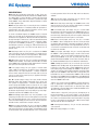
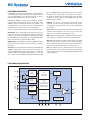
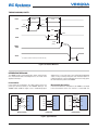
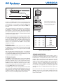
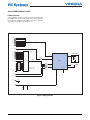
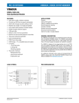
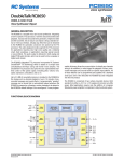
V8600A RC Systems voice synthesizer now you’re talking! V8600A Lead-free Pb-free RoHS Compliant CMOS, 5 Volt-only Voice Synthesizer Module FEATURES •High speech quality, unlimited vocabulary •Converts any ASCII text into speech automatically •Add/modify messages by simply editing a text file •Requires only a single + 5 V supply and speaker •CMOS design – TTL compatible inputs and outputs •User programmable greeting and default settings •Flexible exception dictionary support •2 KB input buffer for “print-and-forget” operation •Software control of all voice parameters •1 W audio output power directly drives an 8 ohm speaker •Playback of sound files: – Real-time PCM and ADPCM – Prerecorded on board, up to 2 minutes APPLICATIONS •Tone generation: – Three voice musical – Dual sinusoidal – DTMF (Touch-Tone) dialer •Robotics •Talking OCR systems •ATM machines •Remote diagnostic reporting •Industrial controllers •Vending and ticketing machines •Electronic test and measurement •Security and warning systems •Aids for the orally or visually disabled •Meeting federal ADA requirements •Low power: – 55 mW typ active – 5 mW typ idle – 4 µW typ standby •Three built-in interfaces: – Microcontroller bus – Asynchronous serial (UART) port – Parallel printer port PIN CONFIGURATION V8600A Hardware Manual Rev 05 Revised 07/10/09 GENERAL DESCRIPTION The V8600A is a full-featured voice synthesizer based on RC Systems’ DoubleTalk RC8650 chipset. The V8600A automatically converts plain English ASCII text into a high quality male voice, requiring only a 5 V power supply and speaker for operation. The V8600A is designed to be piggy-backed onto a host PCB, such as a system’s controller board, using two 12-pin headers. An 8-bit bidirectional data bus and read/write control pins enable the V8600A to be easily interfaced to virtually any microcontroller bus. Stand-alone applications are also possible with the V8600A’s built in printer and serial ports. For additional information about using and programming the V8600A, please refer to the DoubleTalk RC8650 Chipset User’s Manual, available from www.rcsys.com. 1 © 1999 – 2009 RC Systems, Incorporated V8600A RC Systems voice synthesizer now you’re talking! PIN DEFINITIONS last write operation, BUSY will remain High until room becomes available. D0-D7 Data Bus (input/output, active High, 3-state). These pins form an 8-bit bidirectional data bus between the V8600A and the host. When WR# is Low, the Data Bus is placed in the input mode (hostgV8600A). When RD# is Low, the bus is placed in the output mode (V8600Aghost). When RD# is High, the Data Bus is held in the high-impedance state. TXD Transmit Data (output, active High). This pin transfers serial data to the host, least significant bit (LSB) first. RXD Receive Data (input, active High). The V8600A receives serial data from the host on this pin, LSB first. RXD contains an internal pull-up resistor and may be left unconnected. RES# Reset (input, active Low). A Low on this pin forces a hardware reset: speech production is immediately halted, the input buffer is cleared and the status flags and voice parameters (volume, speed, pitch, etc.) are reset to their power-up states. SEN Serial Enable (input, active High). This pin is used to enable the optional RS-232 transceiver chip on the V8600A PCB (see “RS232 transceiver option”). Setting this pin Low will power-down the transceiver chip, reducing overall power consumption. SEN may be left unconnected if the transceiver option is not installed. As shown in the Block Diagram, the V8600A contains an internal power-on reset (POR) circuit, allowing the Reset pin to be left unconnected in most applications. Because the POR circuit drives the Reset pin through a 47 kΩ resistor, it will not contend with external circuitry connected to the Reset pin. Caution: If external voltages are present on the V8600A’s pins before VCC is applied (therefore exceeding the maximum VIH rating), the internal POR circuit may not operate reliably. In this case, RES# must be driven from an external source. CTS# Clear to Send (output, active Low). This pin is Low when the V8600A is able to accept data from the host. CTS# goes High momentarily after a character is received via the RXD pin, acknowledging receipt of each character. If the input buffer becomes full as a result of the last character received, CTS# will remain High until room becomes available. RD# Read (input, active Low). This pin is used to transfer V8600A status information to the host via the Data Bus. A Low gates the status onto the Data Bus and turns on the output drivers. RD# contains an internal pull-up resistor and may be left unconnected. SYNC Sync (output, active High). This pin is normally High when the V8600A is active (producing output). It can be used to control external devices, such as a transmitter or telephone DAA. SYNC is driven by the RC8650’s TS pin; thus its polarity and state can be programmed with the RC8650’s TS Pin Control command. Refer to the DoubleTalk RC8650 Chipset User’s Manual for further details. WR# Write (input, active Low). This pin is used to transfer data to the V8600A via the Data Bus. The contents of the Data Bus are written to the V8600A at the rising edge of Write. WR# contains an internal pull-up resistor and may be left unconnected. STBY# Standby (input, active Low). A Low on this pin causes the V8600A to enter Standby mode. All port handshake lines are driven to their false (“not ready”) states, and the V8600A draws minimum current (0.8 µA typ). During standby, the V8600A is not able to respond to any input pin except STBY# and RES#. Returning STBY# High causes the V8600A to enter Idle mode (1 mA typ drain); the handshake lines are re-asserted and the V8600A is able to accept input again. If the V8600A entered standby due to an RC8650 Sleep Timer event, driving this pin Low for 250 ns or longer then High will return the V8600A to Idle mode. LINE Line (output, analog). This pin supplies a low-level audio signal suitable for connection to an external low pass filter/power amplifier circuit. The output amplitude is a function of both the volume control setting and Volume command. LINE can also be used as a remote volume control input (see “Application Example: Remote Volume Control”). SP+, SP– Speaker (output, analog). These pins provide a filtered, differential audio signal capable of delivering up to 1 W into an 8 ohm speaker. The output power is a function of both the volume control setting and RC8650 Volume command. The SP+ output is AC-coupled, allowing ground-referenced loads to be connected between SP+ and ground (at one-fourth the power, however, since the effective output voltage is cut in half). Both pins go into a highimpedance state when the V8600A is idle or asleep. STBY# is also used to restore the V8600A to its factory default settings. To prevent this from happening unintentionally, make sure that STBY# is High no later than 0.5 sec after RES# goes High. See Appendix A: Restore Mode in the DoubleTalk RC8650 User’s Manual for additional information. STBY# contains a “dynamic” pull-up resistor, allowing the pin to be left unconnected if it is not used. If STBY# is used, the internal pullup resistor is automatically disconnected from the pin when the pin is driven Low in order to reduce overall current drain. The pullup resistor is automatically reconnected when STBY# is driven High, after Idle mode has been re-established. ACK# Acknowledge (output, active Low). This pin produces a 9 µs low-going pulse after each successful write operation over the Data Bus. If the input buffer becomes full as a result of the last write operation, the Acknowledge pulse will not occur until room becomes available. ACK# is inactive when using the serial port. GND Ground (ground reference). This pin must be connected to system ground. BUSY Busy (output, active High). This pin is Low when the V8600A is able to accept data from the host. BUSY goes High momentarily after each write operation over the Data Bus, acknowledging receipt of each character. If the input buffer becomes full as a result of the VCC Power Supply Voltage (+ 5 V ± 10%). 2 V8600A RC Systems voice synthesizer now you’re talking! FUNCTIONAL DESCRIPTION bps. The V8600A determines which baud rate to use by measuring the duration of the shortest High or Low period of the first character received on the RXD pin. The baud rate can also be optionally “strapped,” using three jumpers on the V8600A PCB. See “Fixed baud rate option” for details. The V8600A is a complete, self-contained text-to-speech system. It can be interfaced to a microcontroller bus like a static RAM or I/O port, connected directly to a PC’s parallel printer port, or, with appropriate signal conditioning, to an RS-232 serial port. Operating the V8600A is simply a matter of writing (or “printing,” if connected to a printer port) the text that is to be spoken to the V8600A. Software commands that control voice attributes, such as speed and pitch, are issued the same way, allowing them to be embedded in text for dynamic control of the speech output. Controller. The controller is responsible for processing text and commands from the host and converting input text into speech. Tone generation and I/O port flow control are also performed by the controller. Flash. 1 MB of flash memory contains the internal operating system and text-to-speech algorithms. This memory is also used to store sound files, a user dictionary and greeting message. Refer to the Functional Block Diagram for the following description. Data Register. This is an 8-bit register into which ASCII text, commands, tone generator and PCM data are written from the parallel Data Bus D0-D7. A host microcontroller can write data to this register by placing the data on the Data Bus and asserting the WR# signal. Data is latched on the rising (trailing) edge of WR#. RAM. 4 KB of static RAM provides 2 KB storage for the input buffer and a 2 KB audio sample buffer for the DAC and tone generators. DAC, LPF. An 8-bit digital to analog converter converts the digital speech samples from the Controller into a low level analog signal, which is presented to the input of an antialiasing, four-pole low pass filter (LPF). The filter cutoff frequency is nominally 3.5 kHz. Status Register. This 8-bit register contains the V8600A status flags. The host can read this register over the Data Bus by asserting the RD# signal. Amp. The amplifier takes the smoothed signal from the LPF and boosts the power to a level sufficient to drive an 8 ohm speaker. High efficiency and noise rejection are achieved with the bridge-tied-load output configuration. Serial Port. The Serial Port provides a bidirectional link between the V8600A and serial devices, such as a computer’s RS-232 port. This allows the V8600A to be remotely located, such as in a stand-alone synthesizer. The Serial Port operates with 8 data bits, 1 or more stop bits, no parity, and any standard baud rate between 300 and 115200 FUNCTIONAL BLOCK DIAGRAM 3 V8600A RC Systems voice synthesizer now you’re talking! ELECTRICAL SPECIFICATIONS ABSOLUTE MAXIMUM RATINGS* Supply voltage, VCC . . . . . . . . . . . . . . . . . . . . . . . – 0.3 V to + 6.5 V DC input voltage, VI . . . . . . . . . . . . . . . . . . . – 0.3 V to VCC + 0.3 V Operating temperature, TA. . . . . . . . . . . . . . . . . . . . 0 °C to + 70 °C Storage temperature, TS . . . . . . . . . . . . . . . . . . – 55 °C to + 125 °C * WARNING: Stresses greater than those listed under “Absolute Maximum Ratings” may cause permanent damage to the device. This is a stress rating only; operation of the device at any condition above those indicated in the operational sections of these specifications is not implied. Exposure to absolute maximum rating conditions for extended periods may affect device reliability. Figure 1. Test Circuit DC CHARACTERISTICS TA = 0 °C to + 70 °C, VCC = + 5 V ± 10% Symbol Parameter Min Typ Max Unit Test Conditions VIL Input voltage, Low – 0.3 0.8 V VIH Input voltage, High 2.8 VCC + 0.3 V VHYR Input hysterisis, RES# 0.2 1.8 V VOL Output voltage, Low 0.3 0.5 V V IOL = 6 mA IOL = 2 mA VOH D0 – D7 All other outputs Output voltage, High D0 – D7 VCC – 0.5 V IOH = – 6 mA All other outputs VCC – 0.5 V IOH = – 2 mA – 10 – 120 10 µA µA µA VI = 0 V VI = 0 V VI = VCC ± 5 µA VI = 0 to VCC IIL Input load current, Low IIH D0 – D7 All other inputs Input load current, High IOZ Output leakage current, D0 – D7 RL Output load impedance, SP+, SP– POUT ICC SP output power Supply current (Note 1) Active Idle Sleep/Standby W 8 W RL = 8 W f = 1 kHz 35 3 20 mA mA µA All outputs open; all inputs = VCC 40 mA 1 11 1 0.8 Program (Note 2) 1 Add 5 mA (typ) if RS-232 transceiver option is installed. 2 Applies during internal programming operations: greeting message, dictionary, sound library and microcode updates. 4 V8600A RC Systems voice synthesizer now you’re talking! AC CHARACTERISTICS TA = 0 °C to + 70 °C, VCC = + 5 V ± 10% Symbol Parameter Min Typ Max Unit RD#i to Data valid delay 25 61 ns tDRZ tSDW RD#h to Data float delay Data setup to WR#h delay 23 61 25 ns ns tHWD Data hold from WR#h delay 5 ns tWWR RD# pulse width Low tDWB tWAK WR#h to BUSYh, CTS#h delay ACK# pulse width Low tWRS RES# pulse width Low tDRV 250 RES# recovery delay tWSBL STBY# pulse width Low ns 15 9 µs Note 1 µs Notes 2, 3 After power on / VCC stable During operation tDRR Test Conditions 1 3 ms µs 2 To enter Standby mode To exit Standby mode (Sleep Timer invoked) ms 5 ms 250 ns 1 Applies to the BUSY and CTS# pins and RDY status flag. Note 4 2 STBY# must be High no later than 0.5 sec after R ES# goes High. 3 Reset timings apply only when Reset is driven from an external source. The V8600A contains an internal power-on reset circuit, thus Reset may be left unconnected. 4 V8600A performs internal initialization; all outputs will be floating (except ACK#, which will be High) and the status flags undefined. Do not attempt to send data to the V8600A during this period. TIMING DIAGRAMS Figure 2. Reset Waveform Figure 3. Standby Waveform 5 V8600A RC Systems voice synthesizer now you’re talking! TIMING DIAGRAMS, CONT’D Figure 4. Bus Interface Waveforms INTERFACING THE V8600A with the PC. It is not usually necessary to utilize both handshaking signals, as they essentially convey the same information (BUSY is used by convention). In this configuration, the host PC simply prints the ASCII text to be spoken to the V8600A. The V8600A includes microcontroller bus, printer, and serial interfaces. Detailed schematics illustrating their uses are shown in the Application Examples. Printer Interface Microcontroller Bus Interface In the printer port configuration, the STB# output from the PC’s printer port connects directly to the V8600A’s WR# pin. The V8600A’s ACK# and BUSY outputs serve as handshaking signals µC V8600A RD# In the microcontroller bus configuration, the V8600A is connected to the microcontroller in the same manner as a static RAM. The V8600A PRINTER PORT RD# STB# CS# WR# WR# D0-D7 D0-D7 WR# D0-D7 D0-D7 ACK# ACK# BUSY BUSY Figure 5. Typical Interfaces 6 ASYNC DTE RS232C LINE DRVR/RCVR V8600A TXD RXD RXD TXD CTS CTS# V8600A RC Systems voice synthesizer now you’re talking! controller’s read and write signals control all transactions with the V8600A over the system data bus. The CS# signal is derived from the system’s address decoding logic. The V8600A can also be mapped into the system’s I/O space in a similar manner. START Prior to each write to the V8600A, the host controller should read the V8600A’s status by performing a read operation (RD# = Low). The definition of each status bit is described below. READ STATUS REGISTER V8600A Status Bits RDY = 1 ? NO YES WRITE BYTE TO V8600A SYNC. The SYNC bit has the same meaning as the SYNC pin. When set to 1, it means that the V8600A is producing output. SYNC drops to 0 immediately after output has ceased. READ STATUS REGISTER RDY. The RDY bit has the opposite meaning of the BUSY pin. When RDY is set to 1, the V8600A is ready to accept data. RDY drops to 0 momentarily after each write operation over the Data Bus, acknowledging receipt of each character. NO RDY = 0 ? AF. This bit is set to 1 when less than 100 bytes are available in the input buffer, indicating that the buffer is almost full. AF is always 0 in the PCM modes and when using the musical tone generator. YES AE. This bit is set to 1 when less than 100 bytes are remaining in the input buffer, indicating that the buffer is almost empty. AE is always 1 in the PCM modes and when using the musical tone generator. NO 15 µs TIMEOUT ? YES WRITE COMPLETE Figure 6. Recommended Method of Writing Data Via the Microcontroller Bus Interface STBY. This bit is set to 1 when the V8600A is in Standby mode. Figure 6 illustrates the recommended method of writing data to the V8600A’s microcontroller interface. This method should be used for writing all types of data, including text, commands, tone generator and real time audio data. Serial Interface The V8600A’s asynchronous serial port enables the V8600A to be used with a microcontroller or PC’s communications port. This port operates with 8 data bits (LSB first), 1 or more stop bits, no parity, and any standard baud rate between 300 and 115200 bps. Baud rate selection can be either automatic or jumper selectable. In this configuration, the host system simply outputs the ASCII text to be spoken to the V8600A. Note from the AC Characteristics that the V8600A can take up to 15 µs (tDWB) for each byte to be accepted. Because of this, it is imperative that the driver wait for RDY to drop to 0 after each byte is written. The reason for this is to avoid overwriting the byte just written the next time the routine is called, which can result in the loss of data. Waiting for RDY to drop to 0 ensures that it will not falsely show that the V8600A is ready for another byte the next time the output routine is called. Because the V8600A’s serial port I/O pins operate at TTL levels, the addition of (at most) two RS-232 line drivers and one receiver will be necessary if the host system operates at RS-232 voltage levels. Numerous 5 V-only transceiver chips are available that generate the ± 10 V RS-232 voltage levels from the system’s + 5 V supply. See “RS‑232 transceiver option” for more information. If a system interrupt can occur while waiting for RDY to become 0, or if RDY cannot otherwise be checked at least once every 8 µs, a software timeout should be enforced to avoid hanging up in the wait loop. The time RDY stays 0 is relatively short (8 µs min.) and can be missed if the loop is interrupted. The timeout should be at least 15 µs, which is the maximum time for RDY to drop to 0 after writing a byte of data. In non time-critical applications, the output routine could simply delay 15 µs or longer before exiting, without checking for RDY = 0 at all. Baud rate detection The V8600A includes an automatic baud rate detection mechanism, enabling it to operate at any standard baud rate between 300 and 115200 bps. The baud rate is determined from the first character received on the RXD pin, based on the shortest High or Low period detected in the input stream. This period is assumed to be the bit rate of the incoming data. 7 V8600A RC Systems voice synthesizer now you’re talking! Figure 7. Baud Rate Detection Timing C101 through C105 are 0.1 µF 0805 ceramic chip capacitors. U101 may be a MAX202/232A (SO-16 narrow package) or MAX222/242 (SO18 wide package). Copper tracks marked with “X” must be cut before installing U101. In order for the V8600A to determine the incoming baud rate, there must be at least one isolated “1” or “0” in the input character. The CR character, 0Dh, is recommended for locking the V8600A’s baud rate. The character is not otherwise processed by the V8600A; it is discarded. If the measured bit period is determined to be a valid baud rate, the V8600A will acknowledge lock acquisition by transmitting the ASCII character “L” (4Ch) on the TXD pin. (Note that nothing will be transmitted if the baud rate has been programmed for a fixed rate.) The baud rate will remain locked unless changed with the baud rate command, or the V8600A is reset. Note: The measurement cycle ends when there have been no Highto-Low nor Low-to-High transitions on the RXD pin for at least 75 ms. Consequently, the V8600A will ignore any data sent to it for a period of 75 ms after the “lock-on” character has been received. The CTS# pin is driven High during this time, and the acknowledgment character is not transmitted until the V8600A is actually ready to accept data. See Figure 7. Fixed baud rate option The baud rate can also be set with jumpers JP1, JP2, and JP3 on the V8600A PCB as shown in Figure 8. For baud rates above 19200 automatic detection must be used, or programmed with the RC8650 Baud Rate command. JP3 JP2 JP1 Baud Rate 2-3 2-3 2-3 2-3 1-2 1-2 1-2 1-2 2-3 2-3 1-2 1-2 2-3 2-3 1-2 1-2 2-3 1-2 2-3 1-2 2-3 1-2 2-3 1-2 300 600 1200 2400 4800 9600 19200 Auto-detect (default) Figure 8. PCB Serial Port Options Note: The copper trace connecting jumper pins 1-2 must first be cut on the PCB, if that jumper is to be changed to pins 2-3. For example, to set the baud rate to 9600, cut the trace connecting JP2 pins 1 and 2 and install a jumper between pins 2 and 3. SPEAKER CONSIDERATIONS An often taken-for-granted component of voice synthesis systems is the speaker. Considering how greatly the overall sound quality can be affected by the size and quality of the speaker used, it is usually prudent to test several different speakers under actual operating conditions, before making a final selection. Medium-size (3” to 5”) speakers are ideal for speech reproduction, while smaller speakers (such as the common 2” garden-variety type) suffer from lack of sufficient bass response to accurately reproduce the speech signal. If room permits in your application, use a high-quality speaker with good low-end response. Adding baffling around the speaker can also help. RS-232 transceiver option The V8600A’s serial port operates at 0/+ 5 V levels, which is directly compatible with most microcontroller serial ports. If an RS-232 connection is required, such as to a PC’s communications port, an RS-232 transceiver is required to convert the 0/+ 5 V levels of the V8600A to the ± 10 V voltage levels of the RS-232 port. The transceiver may be located on the board to which the V8600A is mounted, or on the V8600A PCB itself as shown in Figure 8. The V8600A supports four of the more popular RS-232 transceiver chips. The industry standards MAX202 and MAX232A are the most economical choices. For power-sensitive applications the MAX222 or MAX242 should be used, because they can be shut down via the SEN pin. In all cases, C101 through C105 must be installed. Don’t overlook the Tone control (nX command) built into the V8600A. If you must use a small speaker, setting the Tone to the bass setting (0X) can help pick up the slack of the poor low-end response of the speaker. 8 V8600A RC Systems voice synthesizer now you’re talking! APPLICATION EXAMPLES Driving Single-Ended Loads Phone Line Interface Single-ended (ground-referenced) loads may be driven directly from the V8600A’s SP+ pin. However, a noticeable “click” may be present when speech begins and ends. The circuit shown here will help minimize this effect by keeping the SP+ pin biased at VCC/2. The value of C will depend on the impedance of the load — 100 µF minimum for 8 ohm loads. These circuits can be used in applications requiring connection to a telephone line. The circuit in Figure 11 utilizes a Xecom (www. xecom.com) XE0068 telephone DAA, which provides the interface between the V8600A and telephone network. This circuit is ideal for low production quantity applications because the DAA is already FCC Part 68 registered. The PCB layout should employ power and ground planes to minimize coupling of switching noise into the audio path. Figure 12 is a lower-cost implementation using a Xecom XE056J telephone DAA. This circuit is well suited for high volume applications due to the significantly lower cost DAA. The DAA is not FCC registered, however, so the product utilizing this circuit must be approved and certified by the FCC. Figure 9. Driving Single-Ended Loads Remote Volume Control Although the V8600A has no provision for an off-board volume control, one can be used by connecting a 10 kΩ pot between the Line pin and ground. For maximum dynamic range, the V8600A volume control should be adjusted fully clockwise. Figure 11. Phone Line Interface (FCC Registered) Figure 10. Remote Volume Control Figure 12. Phone Line Interface (FCC Compliant) 9 V8600A RC Systems voice synthesizer now you’re talking! APPLICATION EXAMPLES, CONT’D ISA Bus Synthesizer A PC-compatible (ISA bus) synthesizer can be constructed using the V8600A and a small amount of glue logic. In this implementation, the board is mapped into the system as an IO port. Switch bank SW1 selects the I/O address the board will use. Figure 13. ISA Bus Synthesizer 10 V8600A RC Systems voice synthesizer now you’re talking! APPLICATION EXAMPLES, CONT’D Stand-Alone Synthesizer dropout voltage (35 mV at 100 mA), and constantly monitors the output voltage, this circuit is ideal for battery-powered applications. This circuit shows how a complete stand-alone synthesizer can be constructed using only the V8600A and two inexpensive support chips — a MAX202 (a low cost version of the industry standard MAX232) to convert the serial RS-232C signal levels to and from TTL levels, and a Texas Instruments TPS7350Q to provide the regulated + 5 V supply and system reset signal. The synthesizer can be connected to virtually any source via the serial or parallel ports provided. Because the TPS7350Q has very low quiescent current and The 68 Ω resistor at the headphone jack provides balance between relative speaker volume and headphone volume. It also improves headphone S/N ratio, provides short-circuit protection, and gives wider, useful dynamic range of the volume control. Figure 14. Stand-Alone Synthesizer 11 V8600A RC Systems voice synthesizer now you’re talking! MECHANICAL DATA The V8600A may be secured to the host board with self-locking nylon standoffs or threaded spacers at the four corner mounting hole locations. All connections to the V8600A are made through two standard 12pin socket strips. The socket strips mate with any of the popular 0.025” square post headers with 0.100” center pin spacing. The posts generally can be of any height necessary to provide clearance between the V8600A and components on the host PCB. All socket contacts are gold plated. 12 V8600A RC Systems voice synthesizer now you’re talking! COMPARISON OF THE V8600A AND V8600/V8601 Item I/O pins V8600A Pin 23 V8600/V8601 STBY#: multifunction standby/test TEST: perform self-test Pin 22 SYNC: set/clear/automatic; programmable polarity SYNC: automatic, active High only Pin 21 Renamed CTS# (Clear to Send) DTR# (Data Terminal Ready) Pin 20 SEN (Serial Enable) DSR# (Data Set Ready) Memory Input buffer 2.0K V8600: 2.7K V8601: 26K Exception 16K non-volatile (Note: internal format dictionary of dictionary has changed; V8600 dictionaries must be recompiled) V8600: 2.7K volatile (shared with input buffer) User-settable defaults Recorded sound V8601: 26K non-volatile (shared with input buffer) Non-volatile, user-definable default settings and greeting message V8600: none V8601: default settings only Up to 130 seconds None Baud rate selection Automatic, programmable or jumper-selectable Automatic only RS-232 transceiver External or on-board External only Performance† Significantly more responsive; entire voice speed range increased Status obtainable via Speech start = “s” serial port† Speech stop = “t” Buffer almost empty (<100 bytes) = “e” Buffer almost full (>1900 bytes) = “f” Baud rate lock confirmation = “l” Sleep mode confirmation = “p” Speech start = “B” Speech stop = “E” Baud rate lock confirmation = “L” Sleep mode confirmation = “S” Parameter high/low limits Wrap or saturate (programmable) Wrap only Sleep mode Sleep timer or STBY# pin Sleep timer only RES# or STBY# pins RES# pin only Power supply tolerance 5 V ± 10% 5 V ± 5% Supply current (typ) 11 mA 48 mA 1 mA 15 mA 0.8 µA 50 µA Via PC serial port Must replace EPROM Enter Exit Active Idle Sleep Upgrades/updates † In V8600 Compatibility Mode (the default), the V8600A uses the V8600/V8601 speed range and status responses. Program the RC8650’s POR.7 bit to “1” to disable compatibility mode. 13 Specifications written in this publication are believed to be accurate, but are not guaranteed to be entirely free of error. RC Systems reserves the right to make changes in the devices or the device specifications described in this publication without notice. RC Systems advises its customers to obtain the latest version of device specifications to verify, before placing orders, that the information being relied upon by the customer is current. In the absence of written agreement to the contrary, RC Systems assumes no liability relating to the sale and/or use of RC Systems products including fitness for a particular purpose, merchantability, for RC Systems applications assistance, customer’s product design, or infringement of patents or copyrights of third parties by or arising from use of devices described herein. Nor does RC Systems warrant or represent that any license, either express or implied, is granted under any patent right, copyright, or other intellectual property right of RC Systems covering or relating to any combination, machine, or process in which such devices might be or are used. RC Systems products are not intended for use in medical, life saving, or life sustaining applications. Applications described in this publication are for illustrative purposes only, and RC Systems makes no warranties or representations that the devices described herein will be suitable for such applications. 1609 England Avenue, Everett, WA 98203 Phone: (425) 355-3800 www.rcsys.com