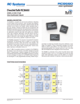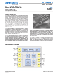
1
RC SYSTEMS
V-STAMP VOICE SYNTHESIZER
V-Stamp™
CMOS, 3.3 Volt / 5 Volt
Voice Synthesizer Module
Features
• Based on RC Systems’ RC8660 chipset
• Integrated text-to-speech processor:
–
–
–
–
High voice quality, unlimited vocabulary
Converts any ASCII text into speech automatically
Add/modify messages by simply editing a text file
On-the-fly control of speed, pitch, volume, etc.
• Four channel, 8-bit A/D converter
• Record, download, upload, and play sound files:
–
–
–
–
Record and/or download to onboard recording memory
Internal file system for easy management of recordings
Data logging mode
Recording times from 130 sec to 15 min available
• Tone generation:
– Three voice musical
– Dual sinusoidal
– DTMF (Touch-Tone) dialer
Applications
Robotics
Electronic test and measurement
GPS navigation systems
Meeting federal ADA requirements
Talking e-mail/telecommunications
Remote diagnostic reporting
ATM machines
Dial-up information systems
Vending and ticketing machines
Industrial controllers
Security and warning systems
Aids for the orally or visually disabled
• Flexible user exception dictionary:
–
–
–
•
•
•
•
Change the pronunciation of any input string based on
spelling and context
Convert encrypted data into meaningful messages
Trigger tone generation, message playback, voice changes
8 KB input buffer for “print-and-forget” operation
1 W audio output power can directly drive an 8 ohm speaker
Standard asynchronous serial interface
Low power (typ @ 3.3 V, excluding audio power amplifier):
– 6 mA active
– 600 µA idle
– 100 nA standby
General Description
The V-Stamp is a feature-rich, self-contained voice/sound synthesizer
and recorder, measuring only 1.7 square inches (10.9 cm2) in size.
Among the V-Stamp’s many features are text-to-speech conversion,
audio recording and playback, musical and sinusoidal tone generation,
a telephone dialer and four-channel A/D converter. All features are accessed using a standard logic-level serial interface.
V-Stamp Product Summary
Order
Number
The V-Stamp mates with two standard, 12-pin PC board connectors.
Separate power pins are provided for the onboard digital and audio
subsystems, allowing for several possible output power and power consumption combinations.
Operating
Voltage
Recording
Capacity *
VS5130
5V
130 sec
RC8660-1
VS3130
3.3 V
130 sec
RC86L60-1
VS3910
3.3 V
910 sec
RC86L60-3
Chipset
* Based on 8 kHz sampling rate with ADPCM encoding
For additional information about using and programming the V-Stamp,
please refer to the DoubleTalk RC8660 Chipset User’s Manual, available from http://www.rcsys.com.
V-Stamp User’s Manual Rev 1.1B
Revised 8/10/05
© 2004, 2005 RC Systems, Incorporated
RC SYSTEMS
V-STAMP VOICE SYNTHESIZER
Pin Configuration
Typical Application Circuit
�����������
��������
������
��
��
�� �� �� ��
�����������
��� ���
����
��
���
���
���
���
������
�����
����
�����
���
���
��
�
���
����
���
�����
�����
����
���
���
����
����
����
����
���
���
�����
������
���
���
���
���
������
������
�
�
�
�
�
�
�����
������
���
���
���
���
����
��
�����
����
���
���
���
�������
�����
����
����
��
��
��
��
��
���
���
����
���
�����
�����
���
��
Functional Block Diagram
�����������������
����������
�����
�������
���
���
����
���������
��
���
�����
�
�
����
������
�������
���
���
���
����
���������
���
�����
���
�����
������
�����
�����
����
����
���
���
���
���
������
�������
�����
���������
� ��
���
�
��
�
��
���
����
���
������
�
���
���
��
RC SYSTEMS
V-STAMP VOICE SYNTHESIZER
Pin Descriptions
Pin Name
Type
Name and Function
LINE
INPUT/
OUTPUT
LINE: High impedance, unfiltered audio output; also feeds into onboard audio subsystem. Output voltage range is
from 0 V to VCC. External audio sources may also be resistively summed with the V-Stamp’s audio and amplified
through this pin.
SP +
SP –
OUTPUT
SPEAKER: Low impedance, filtered, differential audio output that can deliver up to 1 W into an 8 ohm load.
Output power is a function of the voltage on the VPA pin and Volume command setting. A DC voltage of VPA / 2
is present on each pin when MUTE# is High; both pins go into a high-impedance state when MUTE# is Low. Do
not connect either pin to a low impedance ground-referenced load without a DC blocking capacitor.
TS
OUTPUT
TALK STATUS: Indicates when the V-Stamp is active. TS can be used to enable devices such as a transmitter,
telephone, or audio amplifier. The pin’s polarity is programmable, and can be activated automatically or under
program control.
SUSP#
INPUT
SUSPEND: Suspends audio output when Low, allowing playback to be paused. When High, playback resumes
at the point output was suspended. During recording operations, SUSP# will suspend recording when Low. Connect this pin to a High level if not used.
MUTE#
INPUT
MUTE: Shuts down the audio subsystem when Low, reducing the VPA pin current to less than 1 µA. The SP pins
also enter a high-impedance state when MUTE# is Low. Connecting this pin to the TS pin will cause the amplifier circuit to automatically shut down whenever the V-Stamp is inactive, thus conserving power.
AN0 – AN3
INPUT
A/D CONVERTER INPUTS: Analog to digital converter input pins. Analog signals sampled on these pins can
be read through the serial interface, or stored in recording memory. Leave any unused pins unconnected.
OUTPUT
A/D CONVERTER AMPLIFIER: Connecting an operational amplifier between these pins allows the input voltage to all four A/D converter input pins to be amplified with one operational amplifier. Leave these pins unconnected if not used.
AMPIN
AMPOUT
INPUT
RXD
INPUT
TXD
OUTPUT
TRANSMIT DATA: Asynchronous serial data output used to read information out of the V-Stamp.
CTS#
OUTPUT
CLEAR TO SEND: The CTS# pin is Low when the V-Stamp is able to accept data. If the input buffer becomes
full as a result of the last byte received, CTS# will go High and remain High until room becomes available.
BRS0 –
BRS3
INPUT
BAUD RATE SELECT: Programs the V-Stamp’s serial port baud rate. Both the RXD and TXD pins are programmed to the rate set by these pins. Connecting BRS0 – BRS3 to a High level allows the V-Stamp to automatically detect the incoming baud rate.
STBY#
INPUT
STANDBY/INIT: Dual function pin which either puts the V-Stamp in Standby mode or initializes the V-Stamp’s
internal parameter memory. STBY# must be High on the rising edge of RES#.
RECEIVE DATA: Asynchronous serial data input used to send text, data and commands to the V-Stamp. Uses
standard protocol of 8 data bits,1 stop bit, no parity.
Driving STBY# Low for 250 ms or longer causes the V-Stamp to enter Standby mode. The CTS#
pin is driven High (“not ready” state), and the input buffer is cleared. During standby, the V-Stamp draws the
minimum possible current (100 nA typ @ 3.3 V), but it is not able to respond to any input pin except STBY# and
RES#. Returning STBY# High causes the V-Stamp to enter Idle mode (600 µA typ); the CTS# pin is driven Low
and the V-Stamp will be able to accept input again. If the V-Stamp entered standby due to a Sleep Timer event,
driving STBY# Low for 250 ns or longer then High will return the V-Stamp to Idle mode.
Driving STBY# Low for less than 250 ms initializes the V-Stamp’s non-volatile parameter memory.
The greeting message and user dictionary are erased, and all voice parameters and register settings are restored
to their factory default settings. The audio recording memory is not affected. The V-Stamp then announces its
version number via the LINE and SP pins.
Connect this pin to a High level if not used.
RES#
INPUT
RESET: A Low immediately terminates all activity and sets all pins to a predetermined state. During power-up,
RES# must be held Low a minimum of 1 ms after VCC has stabilized in the proper voltage range. All pins will be
valid within 2 ms after reset.
Table 1. Pin Descriptions
RC SYSTEMS
Pin Name
V-STAMP VOICE SYNTHESIZER
Type
Name and Function
VCC
DIGITAL POWER: +5 V ±0.5 V or +3.3 V ±0.3 V digital subsystem power supply connection.
VPA
AUDIO POWER: Power supply connection for the audio subsystem. Connect this pin to a supply voltage
between +3.0 V and +5.5 V (+5 V recommended in order to achieve maximum power output). If the
audio subsystem is not used (output is taken from the LINE pin instead of the SP pins), this pin may be left
unconnected.
VSS
GROUND: Connect to system ground.
Table 1. Pin Descriptions (Continued)
Functional Description
Touch-Tone Generator
The V-Stamp includes a number of features that make it ideally suited
for any design requiring voice output. The V-Stamp’s major features
are described below. For detailed information about using and programming the V-Stamp, refer to the DoubleTalk RC8660 Chipset User’s
Manual.
The V-Stamp includes an integrated DTMF (Touch-Tone) generator.
This is useful in telephony applications where standard DTMF tones are
used to signal a remote receiver, modem, or access the public switched
telephone network.
Sinusoidal Tone Generator
Text-to-Speech Synthesizer
A precision, dual sinusoidal tone generator can synthesize the tones
often used in signaling applications. The tone frequencies can be
independently set, allowing signals such as call-progress tones to be
generated.
The V-Stamp provides text-to-speech conversion with its integrated
DoubleTalk™ text-to-speech synthesizer. Any English text written to
the V-Stamp is automatically converted into speech. Commands can be
embedded in the input stream to dynamically control the voice, even at
the phoneme level (phonemes are the basic sound units of speech).
Analog-to-Digital Converter
The four channel, 8-bit A/D converter can be used to monitor battery
cell voltages, temperature, and other analog quantities. The ADC can
be programmed on the fly to convert any single channel, or scan up to
four channels repetitively. Data logging and audio recording to the VStamp’s recording memory are also possible through the ADC.
A greeting message can be stored in the V-Stamp that is automatically
spoken immediately after the V-Stamp is reset. Most any of the commands recognized by the V-Stamp may be included as part of the
greeting message, which can be used to set up custom default settings
and/or play a pre-recorded message or tone sequence. An integrated
nonvolatile memory area is also provided for storing a custom pronunciation dictionary, allowing the pronunciation of any character string
to be redefined.
Audio Subsystem
The V-Stamp includes an audio subsystem, comprised of a low-pass
filter and audio power amplifier. This subsystem operates independently
of the V-Stamp’s digital subsystem; a separate power pin, VPA, powers the audio circuits and can be connected to a supply voltage that is
different than VCC. For example, VCC can be connected to 3.3 V to
minimize digital power drain, and VPA connected to 5 V in order to
achieve maximum power output.
Audio Recording and Playback
Up to 15 minutes of recorded messages and sound effects can be stored
in the V-Stamp for on-demand playback. Recordings are stored in
onboard nonvolatile memory, providing zero-power message storage.
Additionally, the V-Stamp can play eight-bit PCM and ADPCM audio
in real time, such as speech and/or sound effects stored in an external
memory or file system.
External audio sources can also be filtered and amplified through the
V-Stamp’s audio system by injecting them into the LINE pin through a
series resistor. If the audio subsystem is not required in an application
(output is taken from the LINE pin instead of the SP pins), VPA may be
left unconnected to further minimize power consumption. The MUTE#
pin may also be used to effectively shut down the audio subsystem when
not in use.
Musical Tone Generator
An integrated, three-voice musical tone generator is capable of generating up to three tones simultaneously over a four-octave range. Simple
tones to attention-getting sounds can be easily created.
RC SYSTEMS
V-STAMP VOICE SYNTHESIZER
Interfacing the V-Stamp
the baud rate according to the logic levels present on the BRS0 – BRS3
pins, as shown in Table 2. Auto-detect enables the serial port to automatically detect the baud rate of the incoming data. The baud rate command (described in the DoubleTalk RC8660 Chipset User’s Manual)
allows the baud rate to be changed at any time, effectively overriding
the first two methods.
All communication with the V-Stamp is performed via the built-in asynchronous serial interface. The serial interface operates with 8 data bits
(LSB first), 1 or more stop bits, no parity, and any standard baud rate
between 300 and 115200 bps.
The V-Stamp’s serial port operates at 0/+5 V or 0/+3.3 V logic levels.
If the host system operates at RS-232C levels (such as a PC’s serial
port), the circuit in Figure 1 can be used to provide the correct voltage
level conversion.
The automatic baud rate detection mechanism is enabled when the
BRS0 – BRS3 pins are all at a High logic level. The baud rate is determined by the shortest High or Low period detected in the input
stream. This period is assumed to be the bit rate of the incoming data;
therefore it is important that there be at least one isolated “1” or “0”
in the input character. The CR character, 0Dh, is recommended for
locking the baud rate. The character is not otherwise processed by the
V-Stamp; it is discarded.
The CTS# pin should be used to control the flow of data to the VStamp. It is not necessary to check CTS# before transmitting every
byte, however. All data is routed through a high speed 16-byte buffer
within the V-Stamp before being stored in the primary buffer. CTS#
may be checked every eight bytes with no risk of data loss.
If the measured bit period is determined to be a valid baud rate, the
V-Stamp acknowledges lock acquisition by transmitting the ASCII character “l” (6Ch) on the TXD pin. The baud rate will remain locked unless
changed with the baud rate command, or the V-Stamp is reset.
Baud Rate Selection
The serial port’s baud rate can be programmed using any of three methods: pin strapping, auto-detect, and by command. Pin strapping sets
BRS3
BRS2
BRS1
BRS0
Baud Rate
L
L
L
L
300
L
L
L
L
L
L
L
H
H
H
L
L
L
H
H
H
H
L
L
L
L
H
H
L
L
H
H
L
L
H
H
L
H
L
H
L
H
L
H
L
600
1200
2400
4800
9600
19200
Auto-detect
38400
57600
115200
All other settings
NOTE The measurement cycle ends when there have been no Highto-Low nor Low-to-High transitions on the RXD pin for 75 ms or
longer. Consequently, the V-Stamp will ignore any data sent to it for a
period of 75 ms after the “lock-on” character has been received. The
CTS# pin is driven High during this time, and the acknowledgment
character is not transmitted until the V-Stamp is actually ready to accept data. See Figure 2.
���������
���
���
����
Auto-detect
�����������������������������
���
���
Figure 2. Baud Rate Detection Timing
Table 2. Baud Rate Options
�������
���
��
�������
���
���
����
���
���
�
��
���
��
��
��
��
��
��
��
�
��
���
���
���
���
���
���
���
���
���
���
���
�
��
��
�
��
�
��
��
�
�
Figure 1. RS-232C Interface
���
�����
�
�����
��
�������
�����������
�
�����
���
����
����
����
����
���
�����
���
���
���
���
���
�
�
�
�
�
�
�
�
�
�������������
����������
RC SYSTEMS
V-STAMP VOICE SYNTHESIZER
Audio Subsystem
the pin can be controlled through the V-Stamp’s serial port using the
RC8660’s TS Pin Control command. With the TS pin’s default setting,
the pin will automatically activate the audio subsystem when required,
and shut it down when it is no longer needed. If an external audio source
needs to use the audio subsystem, it can activate it manually by setting
the TS pin High with the 3K command.
The V-Stamp’s audio subsystem can directly drive an 8 ohm speaker
with up to one watt of output power at VPA = 5 V. If less power is
needed, the VPA pin can be connected to a lower voltage, such as 3.3 V,
which will reduce power consumption. Note, however, that the power
amplifier has been optimized for operation at VPA = 5 V. When operating at voltages lower than this, it is recommended that the V-Stamp’s
software-controlled volume level (nV command) be maintained at lower
settings in order to avoid distortion in the power amplifier — which can
dramatically increase power dissipation and power consumption.
A/D Converter
The V-Stamp’s onboard ADC has the following features:
– Four channels, 8-bit resolution (±2 LSB precision)
– One-shot, continuous, single sweep, and continuous sweep
modes of operation
– Support for external amplification/signal conditioning of all four
ADC channels
The speaker output pins are designed to drive a load differentially.
The benefits of this design compared with a single-ended (ground-referenced) design are many, the most significant being up to four times
greater power output for a given supply voltage, reduced amplifier power dissipation (higher efficiency), better rejection of power supply noise,
and the elimination of a large DC blocking capacitor on the output.
In most applications, analog voltages to be converted by the ADC may
be connected directly to the AN input pins. The minimum and maximum input voltage limits must be observed, however; in many cases this
can be accomplished with a simple resistive divider. Because the CMOS
AN pin input impedances are extremely high, the error introduced by
a resistive divider is minimal. It is also good design practice to include a
small capacitor from the AN pin to ground as a precautionary measure
against noise that may be present on the signal being measured.
Do not attempt to connect a ground-referenced load to either SP pin
directly. Each pin has a DC bias component of VPA / 2 V, which would
result in a high DC current flowing through the load, possibly damaging
the load and/or power amplifier. Instead, connect the load through a
DC blocking capacitor. A minimum value of 100 µF is recommended
for 8 ohm loads.
External audio sources may also be filtered and amplified through the
V-Stamp’s audio subsystem by injecting them into the LINE pin via
a series resistor. The total of the resistor and external signal’s source
impedance should be at least several kW in order to avoid loading the
V-Stamp’s signal excessively, and the signal amplitude must be limited
to between 0 V and VCC.
Applications using the ADC for voice recording will require a microphone and preamplifier. The circuit shown in Figure 3 is suitable for
this purpose, as it offers high gain, low cost, and low power consumption (less than 200 µA typ at supply voltages of 3.3 V to 5 V, including
the current of a second internal amplifier not shown). In addition, the
circuit provides low-pass filtering to prevent undesired frequencies from
reaching the ADC. This circuit should work well with most any electret
condenser microphone.
Power supply consumption can be minimized when the V-Stamp is
not in use by shutting down the audio subsystem with the MUTE# pin.
MUTE# can be connected to a microcontroller’s I/O port pin for direct
control by the application, or it can be connected to the V-Stamp’s TS
pin. Connection to the TS pin offers the greatest flexibility, because
Please refer to the DoubleTalk RC8660 Chipset User’s Manual for
information on programming and using the ADC, as well as how to
record to the RC8660’s recording memory.
���
�����
���
����
�������
��
��
��
����
������
������
�
�����
�
�
�
�
�����
���
�
�
��
�����������
��
����
��
��
�
�
�
�������
��
�������
��
�����
Figure 3. Microphone Preamp & Filter Circuit
��
�����
����������������
��
�����
RC SYSTEMS
V-STAMP VOICE SYNTHESIZER
Electrical Specifications
Absolute Maximum Ratings*
* WARNING: Stresses greater than those listed under “Absolute
Maximum Ratings” may cause permanent damage to the device.
This is a stress rating only; operation of the device at any condition
above those indicated in the operational sections of these specifications is not implied. Exposure to absolute maximum rating conditions for extended periods may affect device reliability.
Supply voltage, VCC and VPA. . . . . . . . . . . . . . . . – 0.3 V to +6.5 V
DC input voltage, VI. . . . . . . . . . . . . . . . . . . . – 0.3 V to VCC +0.3 V
Operating temperature, TA. . . . . . . . . . . . . . . . . . . . 0 °C to +70 °C
Storage temperature, TS. . . . . . . . . . . . . . . . . . . – 55 °C to +125 °C
DC Characteristics
TA = 0 °C to +70 °C, VCC = 3.3 V / 5 V, VPA = 3.3 V / 5 V, VSS = 0 V
Digital Subsystem
Symbol
Parameter
VIL
Input Voltage, Low
VIH
VIA
Input Voltage, High
Analog Input Voltage (AN0-3)
VHYR
Input Hysterisis, RES#
VOL
Output Voltage, Low
VOH
Output Voltage, High
IIL
Input Load Current
RO
LINE Output Resistance
ICC
Supply Current
VCC = 3.3 ± 0.3 V
Min
Typ
Max
Min
Typ
Max
Unit
Test Conditions
– 0.3
0.2VCC
– 0.3
0.2VCC
V
0.7VCC
– 0.3
VCC + 0.3
VCC
0.7VCC
– 0.3
VCC + 0.3
VCC
V
V
0.2
1.8
0.2
1.8
V
0.5
V
IOL = 1 mA
V
IOH = – 1 mA
± 5
µA
VIN = VSS to VCC
10
20
kW
13
1.2
0.2
33
2.5
20
mA
mA
µA
65
mA
0.5
VCC – 0.5
VCC – 0.5
± 4
4
Active
Idle
Standby
10
20
6
0.6
0.1
18
1.5
15
4
35
Program (Note 1)
1
VCC = 5 V ± 0.5 V
All outputs open;
all inputs = VCC
or VSS
Applies during internal programming operations: greeting message, dictionary, sound library and microcode updates.
Audio Subsystem
Symbol
Parameter
VIL
MUTE# Input Voltage, Low
VIH
MUTE# Input Voltage, High
VOS
SP Output Offset Voltage
PO
SP Output Power (THD < 1%)
IPA
Supply Current
VPA = 3.3 ± 0.3 V
Min
Typ
VPA = 5 V ± 0.5 V
Max
Min
Typ
0.4
1.2
Max
0.4
1.2
5
50
0.3
Unit
V
V
5
50
1
330
mV
W
RL = 8 W
RL = 8 W
RL = 8 W
RL = ∞
MUTE# = VSS
PO = 1 W
PO = 0.3 W
PO = 0 W
240
3.8
8
4.9
10
mA
mA
mA
Shutdown
0.01
2
0.01
2
µA
VPA may be left unconnected if output is taken from LINE pin instead of SP pins. It is permissible for VPA to be at a different voltage level than VCC.
Test Conditions
RC SYSTEMS
V-STAMP VOICE SYNTHESIZER
AC Characteristics
TA = 0 °C to +70 °C, VCC = 3.3 V / 5 V, VSS = 0 V
Standby Timing
Symbol
VCC = 3.3 ± 0.3 V
Parameter
tWSBL
Min
VCC = 5 V ± 0.5 V
Max
Min
250
250
8
Max
STBY# Pulse Width Low
To enter Standby mode
To reinitialize parameter memory
250
8
To exit Standby mode (Sleep Timer invoked)
380
250
250
�����
�����
Figure 4. Standby Waveform
Reset Timing
Symbol
tWRS
tDRR
Unit
Parameter
Min
Max
Unit
Notes
Hold RES# Low during power-up
RES# Pulse Width Low
After power on / VCC stable
1
ms
During operation
3
µs
RES# Recovery Delay
2
ms
����
����
����
Figure 5. Reset Waveform
ms
ms
ns
RC SYSTEMS
V-STAMP VOICE SYNTHESIZER
Mechanical Data
�����
�����
��������������
���������
�
��
�����
�����
���
��
��
�����������������������������
��������������������������������
������������������������������
������������������������������
�����
���������
����
�����
�����
��������
Specifications written in this publication are believed to be accurate, but are not guaranteed to be entirely free of error. RC Systems reserves the right to make changes in
the devices or the device specifications described in this publication without notice. RC Systems advises its customers to obtain the latest version of device specifications
to verify, before placing orders, that the information being relied upon by the customer is current.
In the absence of written agreement to the contrary, RC Systems assumes no liability relating to the sale and/or use of RC Systems products including fitness for a
particular purpose, merchantability, for RC Systems applications assistance, customer’s product design, or infringement of patents or copyrights of third parties by or
arising from use of devices described herein. Nor does RC Systems warrant or represent that any license, either express or implied, is granted under any patent right,
copyright, or other intellectual property right of RC Systems covering or relating to any combination, machine, or process in which such devices might be or are used.
RC Systems products are not intended for use in medical, life saving, or life sustaining applications.
Applications described in this publication are for illustrative purposes only, and RC Systems makes no warranties or representations that the devices described herein
will be suitable for such applications.
1609 England Avenue, Everett, WA 98203
Phone: (425) 355-3800 Fax: (425) 355-1098
http://www.rcsys.com