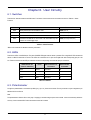
1
To our customers,
Old Company Name in Catalogs and Other Documents
On April 1st, 2010, NEC Electronics Corporation merged with Renesas Technology
Corporation, and Renesas Electronics Corporation took over all the business of both
companies. Therefore, although the old company name remains in this document, it is a valid
Renesas Electronics document. We appreciate your understanding.
Renesas Electronics website: http://www.renesas.com
April 1st, 2010
Renesas Electronics Corporation
Issued by: Renesas Electronics Corporation (http://www.renesas.com)
Send any inquiries to http://www.renesas.com/inquiry.
Notice
1.
2.
3.
4.
5.
6.
7.
All information included in this document is current as of the date this document is issued. Such information, however, is
subject to change without any prior notice. Before purchasing or using any Renesas Electronics products listed herein, please
confirm the latest product information with a Renesas Electronics sales office. Also, please pay regular and careful attention to
additional and different information to be disclosed by Renesas Electronics such as that disclosed through our website.
Renesas Electronics does not assume any liability for infringement of patents, copyrights, or other intellectual property rights
of third parties by or arising from the use of Renesas Electronics products or technical information described in this document.
No license, express, implied or otherwise, is granted hereby under any patents, copyrights or other intellectual property rights
of Renesas Electronics or others.
You should not alter, modify, copy, or otherwise misappropriate any Renesas Electronics product, whether in whole or in part.
Descriptions of circuits, software and other related information in this document are provided only to illustrate the operation of
semiconductor products and application examples. You are fully responsible for the incorporation of these circuits, software,
and information in the design of your equipment. Renesas Electronics assumes no responsibility for any losses incurred by
you or third parties arising from the use of these circuits, software, or information.
When exporting the products or technology described in this document, you should comply with the applicable export control
laws and regulations and follow the procedures required by such laws and regulations. You should not use Renesas
Electronics products or the technology described in this document for any purpose relating to military applications or use by
the military, including but not limited to the development of weapons of mass destruction. Renesas Electronics products and
technology may not be used for or incorporated into any products or systems whose manufacture, use, or sale is prohibited
under any applicable domestic or foreign laws or regulations.
Renesas Electronics has used reasonable care in preparing the information included in this document, but Renesas Electronics
does not warrant that such information is error free. Renesas Electronics assumes no liability whatsoever for any damages
incurred by you resulting from errors in or omissions from the information included herein.
Renesas Electronics products are classified according to the following three quality grades: “Standard”, “High Quality”, and
“Specific”. The recommended applications for each Renesas Electronics product depends on the product’s quality grade, as
indicated below. You must check the quality grade of each Renesas Electronics product before using it in a particular
application. You may not use any Renesas Electronics product for any application categorized as “Specific” without the prior
written consent of Renesas Electronics. Further, you may not use any Renesas Electronics product for any application for
which it is not intended without the prior written consent of Renesas Electronics. Renesas Electronics shall not be in any way
liable for any damages or losses incurred by you or third parties arising from the use of any Renesas Electronics product for an
application categorized as “Specific” or for which the product is not intended where you have failed to obtain the prior written
consent of Renesas Electronics. The quality grade of each Renesas Electronics product is “Standard” unless otherwise
expressly specified in a Renesas Electronics data sheets or data books, etc.
“Standard”:
8.
9.
10.
11.
12.
Computers; office equipment; communications equipment; test and measurement equipment; audio and visual
equipment; home electronic appliances; machine tools; personal electronic equipment; and industrial robots.
“High Quality”: Transportation equipment (automobiles, trains, ships, etc.); traffic control systems; anti-disaster systems; anticrime systems; safety equipment; and medical equipment not specifically designed for life support.
“Specific”:
Aircraft; aerospace equipment; submersible repeaters; nuclear reactor control systems; medical equipment or
systems for life support (e.g. artificial life support devices or systems), surgical implantations, or healthcare
intervention (e.g. excision, etc.), and any other applications or purposes that pose a direct threat to human life.
You should use the Renesas Electronics products described in this document within the range specified by Renesas Electronics,
especially with respect to the maximum rating, operating supply voltage range, movement power voltage range, heat radiation
characteristics, installation and other product characteristics. Renesas Electronics shall have no liability for malfunctions or
damages arising out of the use of Renesas Electronics products beyond such specified ranges.
Although Renesas Electronics endeavors to improve the quality and reliability of its products, semiconductor products have
specific characteristics such as the occurrence of failure at a certain rate and malfunctions under certain use conditions. Further,
Renesas Electronics products are not subject to radiation resistance design. Please be sure to implement safety measures to
guard them against the possibility of physical injury, and injury or damage caused by fire in the event of the failure of a
Renesas Electronics product, such as safety design for hardware and software including but not limited to redundancy, fire
control and malfunction prevention, appropriate treatment for aging degradation or any other appropriate measures. Because
the evaluation of microcomputer software alone is very difficult, please evaluate the safety of the final products or system
manufactured by you.
Please contact a Renesas Electronics sales office for details as to environmental matters such as the environmental
compatibility of each Renesas Electronics product. Please use Renesas Electronics products in compliance with all applicable
laws and regulations that regulate the inclusion or use of controlled substances, including without limitation, the EU RoHS
Directive. Renesas Electronics assumes no liability for damages or losses occurring as a result of your noncompliance with
applicable laws and regulations.
This document may not be reproduced or duplicated, in any form, in whole or in part, without prior written consent of Renesas
Electronics.
Please contact a Renesas Electronics sales office if you have any questions regarding the information contained in this
document or Renesas Electronics products, or if you have any other inquiries.
(Note 1) “Renesas Electronics” as used in this document means Renesas Electronics Corporation and also includes its majorityowned subsidiaries.
(Note 2) “Renesas Electronics product(s)” means any product developed or manufactured by or for Renesas Electronics.
User’s Manual
Renesas Starter Kit for R32C/118
User’s Manual
RENESAS SINGLE-CHIP MICROCOMPUTER
R32C/100 Series
Rev.1.00 2009.02
Disclaimer
By using this Renesas Starter Kit (RSK), the user accepts the following terms. The RSK is not guaranteed to be error free, and the entire
risk as to the results and performance of the RSK is assumed by the User. The RSK is provided by Renesas on an “as is” basis without
warranty of any kind whether express or implied, including but not limited to the implied warranties of satisfactory quality, fitness for a
particular purpose, title and non-infringement of intellectual property rights with regard to the RSK. Renesas expressly disclaims all such
warranties. Renesas or its affiliates shall in no event be liable for any loss of profit, loss of data, loss of contract, loss of business,
damage to reputation or goodwill, any economic loss, any reprogramming or recall costs (whether the foregoing losses are direct or
indirect) nor shall Renesas or its affiliates be liable for any other direct or indirect special, incidental or consequential damages arising
out of or in relation to the use of this RSK, even if Renesas or its affiliates have been advised of the possibility of such damages.
Precautions
This Renesas Starter Kit is only intended for use in a laboratory environment under ambient temperature and humidity conditions. A safe
separation distance should be used between this and any sensitive equipment. Its use outside the laboratory, classroom, study area or
similar such area invalidates conformity with the protection requirements of the Electromagnetic Compatibility Directive and could lead to
prosecution.
The product generates, uses, and can radiate radio frequency energy and may cause harmful interference to radio communications.
However, there is no guarantee that interference will not occur in a particular installation. If this equipment causes harmful interference to
radio or television reception, which can be determined by turning the equipment off or on, you are encouraged to try to correct the
interference by one or more of the following measures;
•
ensure attached cables do not lie across the equipment
•
reorient the receiving antenna
•
increase the distance between the equipment and the receiver
•
connect the equipment into an outlet on a circuit different from that which the receiver is connected
•
power down the equipment when not is use
•
consult the dealer or an experienced radio/TV technician for help NOTE: It is recommended that wherever possible shielded
interface cables are used.
The product is potentially susceptible to certain EMC phenomena. To mitigate against them it is recommended that the following
measures be undertaken;
•
The user is advised that mobile phones should not be used within 10m of the product when in use.
•
The user is advised to take ESD precautions when handling the equipment.
The Renesas Starter Kit does not represent an ideal reference design for an end product and does not fulfil the regulatory standards for
an end product.
ii
Table of Contents
Chapter 1. Preface .................................................................................................................................................. 1
Chapter 2. Purpose ................................................................................................................................................. 2
Chapter 3. Power Supply ........................................................................................................................................ 3
3.1. Requirements ............................................................................................................................................... 3
3.2. Power–up Behaviour .................................................................................................................................... 3
Chapter 4. Board Layout ......................................................................................................................................... 4
4.1. Component Layout ....................................................................................................................................... 4
4.2. Board Dimensions ........................................................................................................................................ 5
4.3. Dual Footprint ............................................................................................................................................... 6
Chapter 5. Block Diagram ....................................................................................................................................... 8
Chapter 6. User Circuitry......................................................................................................................................... 9
6.1. Switches ....................................................................................................................................................... 9
6.2. LEDs ............................................................................................................................................................. 9
6.3. Potentiometer ............................................................................................................................................... 9
6.4. Serial port ................................................................................................................................................... 10
6.5. Debug LCD Module .................................................................................................................................... 10
6.6. Option Links................................................................................................................................................ 10
6.7. Oscillator Sources ...................................................................................................................................... 17
6.8. Reset Circuit ............................................................................................................................................... 17
Chapter 7. Modes .................................................................................................................................................. 19
7.1. Boot mode .................................................................................................................................................. 19
7.2. User Mode .................................................................................................................................................. 19
Chapter 8. Programming Methods ........................................................................................................................ 20
Chapter 9. Headers ............................................................................................................................................... 21
9.1. Microcontroller Ring Headers ..................................................................................................................... 21
9.2. Application Headers ................................................................................................................................... 25
Chapter 10. Code Development ........................................................................................................................... 28
10.1. Overview................................................................................................................................................... 28
10.2. Compiler Restrictions ............................................................................................................................... 28
10.3. Breakpoint Support ................................................................................................................................... 28
10.4. Memory Map............................................................................................................................................. 29
Chapter 11. Component Placement ...................................................................................................................... 31
Chapter 12. Additional Information........................................................................................................................ 32
iii
Chapter 1. Preface
Cautions
This document may be, wholly or partially, subject to change without notice.
All rights reserved. No one is permitted to reproduce or duplicate, in any form, a part or this entire document without the written
permission of Renesas Technology Europe Limited.
Trademarks
All brand or product names used in this manual are trademarks or registered trademarks of their respective companies or
organisations.
Copyright
© 2009 Renesas Technology Europe Ltd. All rights reserved.
© 2009 Renesas Technology Corporation. All rights reserved.
© 2009 Renesas Solutions Corporation. All rights reserved.
Website:
http://www.renesas.com/
Glossary
ADC
Analog to Digital Converter
DAC
Digital to Analog Converter
E8A
“E8A ” emulator
HEW
High-Performance Embedded Workshop
I/O
Input / Output
LCD
Liquid Crystal Display
LED
Light Emitting Diode
MCU
Microcontroller Unit
RSK
Renesas Starter Kit
UART
Universal Asynchronous Receiver / Transmitter
USB
Universal Serial Bus
1
Chapter 2. Purpose
This RSK is an evaluation tool for Renesas microcontrollers.
Features include:
•
Renesas Microcontroller Programming.
•
User Code Debugging.
•
User Circuitry such as switches, LEDs and potentiometer(s).
•
Sample Application.
•
Sample peripheral device initialisation code.
The RSK board contains all the circuitry required for microcontroller operation.
This manual describes the technical details of the RSK hardware. The Quick Start Guide and Tutorial Manual provide details of the
software installation and debugging environment.
2
Chapter 3. Power Supply
3.1. Requirements
This RSK board operates from a 5V DC power supply.
A diode provides reverse polarity protection only if a current limiting power supply is used.
All RSK boards are supplied with an E8A debugger. This product is able to power the RSK board with up to 300mA. When the RSK is
connected to another system then that system should supply power to the RSK.
All RSK boards have an optional centre positive supply connector using a 2.0mm barrel power jack.
Warning
The RSK board is neither under nor over voltage protected. Use a centre positive supply for this board.
3.2. Power–up Behaviour
When the RSK is purchased the RSK board has the ‘Release’ or stand-alone code from the example tutorial code pre-programmed into the
Renesas microcontroller. On powering up the board the user LEDs will start to flash. After 200 flashes or after pressing any switch the
LEDs will flash at a rate controlled by the potentiometer.
3
Chapter 4. Board Layout
4.1. Component Layout
The following diagram shows the top layer component layout of the board.
Figure 4-1: Board Layout
4
4.2. Board Dimensions
The following diagram gives the board dimensions and connector positions. All through-hole connectors are on a common 0.1” grid for
easy interfacing.
Figure 4-2 : Board Dimensions
5
4.3.Dual Footprint
J4
2
4
6
8
10
12
14
16
18
20
22
24
26
28
30
32
34
36
2
4
6
8
10
12
14
16
18
20
22
24
26
28
30
32
34
36
1
3
5
7
9
11
13
15
17
19
21
23
25
27
29
31
33
35
U2
U1
J3
J2
Note:
Pins marked in blue color not available for use on 100 pin package
Figure 4-3 : Dual Footprint Connection
6
1
3
5
7
9
11
13
15
17
19
21
23
25
27
29
31
33
35
J1
Figure 4-4 : R32C118 (LQFP144) fitted on board
Figure 4-5 : R32C118 (LQFP100) fitted on board
7
Chapter 5. Block Diagram
Figure 5-1 shows the RSK board components and their connectivity.
Figure 5-1: Block Diagram
Figure 5-2 shows the E8A connections to the RSK.
USB Cable
Host PC
E8A Module
Pin 1
User Interface Cable
E8A
MCU
E30A
CPU Board
Figure 5-2: E8A RSK Connections
8
Chapter 6. User Circuitry
6.1. Switches
There are four switches located on the RSK board. The function of each switch and its connection are shown in Table 6-1: Switch
Functions
Switch
Function
Microcontroller
RES
When pressed, the microcontroller is reset.
RESn, Pin 19
SW1 / BOOT*
Connects to an IRQ input for user controls.
INT0n, Pin 27 (Port 8, bit 2)
SW2*
Connects to an IRQ line for user controls.
INT1n, Pin 26 (Port 8, bit 3)
SW3*
Connects to an IRQ line for user controls. The same switch may also
INT2n, Pin 25 (Port 8, bit 4)
function as an ADC trigger input.
Table 6-1: Switch Functions
*Refer to the schematic for detailed connectivity information.
6.2. LEDs
There are six LEDs on the RSK board. The green ‘POWER’ LED lights when the board is powered. The orange BOOT LED indicates the
device is in BOOT mode when lit. The four user LEDs are connected to an I/O port and will light when their corresponding port pin is set
low. Table 6-2 below shows the LED pin references and their corresponding microcontroller port pin connections.
LED Reference (As
Colour
Microcontroller Port
Microcontroller
Pin function
Pin Number
shown on silkscreen)
LED0
Green
Port 4 bit 0
78
LED1
Orange
Port 4 bit 1
77
LED2
Red
Port 4 bit 2
75
LED3
Red
Port 4 bit 3
73
Table 6-2: LED Port
6.3. Potentiometer
A single-turn potentiometer is connected to pin AN0 (p10_0, pin 141) of the microcontroller. This may be used to vary the voltage at this pin
between AVCC and Ground.
Note:
The potentiometer is fitted to offer an easy way of supplying a variable analogue input to the controller. It does not necessarily reflect the
accuracy of the controllers ADC. Please see the device manual for details.
9
6.4. Serial port
Serial port UART0 is connected to the standard RS232 header. Serial port UART1 can optionally be connected to the RS232. The
connections to be fitted are listed in the Table 6-3.
Description
Function
Microcontroller
Fit for RS232
Remove for RS232
Port Pin
UART0
Default serial port (TX)
Port 6_3
R47
R70, R59
UART0
Default serial port (RX)
Port 6_2
R41
R28, R29
UART1
Spare Serial Port (TX)
Port 6_7
R59
R47, R70
UART1
Spare Serial Port (RX)
Port 6_6
R28
R29, R41
Table 6-3: Serial Options Links
The board is designed to accept a straight-through RS-232 male-to-female cable.
The second transceiver channels are connected to a 0.1” header, J7. UART2 can be connected to this channel by fitting 0Ω link resistors
to R63 and R64.
6.5. Debug LCD Module
The LCD module supplied with the RSK can be connected to the connector ‘LCD’ for use with the tutorial code. Any module that conforms
to the pin connections and has a KS0066u-compatible controller can be used. The LCD module uses a 4-bit interface to reduce the pin
allocation. No contrast control is provided; this must be set on the display module.
Table 6-4 shows the pin allocation and signal names used on this connector.
The module supplied with the RSK board only supports 5V operation.
LCD
Pin
Circuit Net Name
Device Pin
Pin
Circuit Net Name
Device Pin
1
Ground
-
2
5V Only
-
3
No Connection
-
4
DLCDRS (p2_0)
101
5
R/W (Wired to Write only)
-
6
DLCDE (p2_1)
100
7
No Connection
-
8
No Connection
-
9
No Connection
-
10
No Connection
-
11
DLCDD4 (p2_4)
97
12
DLCDD5 (p2_5)
96
13
DLCDD6 (p2_6)
95
14
DLCDD7 (p2_7)
94
Table 6-4: Debug LCD Module Connections
6.6. Option Links
In this section the default configuration is indicated by BOLD text.
Table 6-5 below describes the function of the option links associated with serial port configuration.
10
Option Link Settings
Reference
R23
R27
R28
R29
R41
R47
R59
R63
R64
R69
R70
R73
Function
Fitted
Alternative (Removed)
Related To
Enables the RS-232 Transceiver
R27
Disables the RS-232 Transceiver
R23
Connects the programming port (Rx) to
Disconnects the programming port (Rx)
R29, R30,
Configuration
external serial connectors
to external serial connectors
R41
Serial Port
Routes the RS-232 serial port (Rx) to
Disconnects the RS-232 serial port (Rx)
R28, R41
Configuration
application board interface (JA6-6)
from application board interface (JA6-6)
Serial Port
Connects serial port RXD0 to CH1 of
Disconnects serial port RXD0 to CH1 of
Configuration
RS-232 transceiver
RS-232 transceiver
Serial Port
Connects serial port TXD0 to CH1 of
Disconnects serial port TXD0 to CH1 of
Configuration
RS-232 transceiver
RS-232 transceiver
Serial Port
Connects the serial programming port
Disconnects the serial programming port
R36, R47,
Configuration
(Tx) to external connectors (not E8A)
(Tx) to external serial connectors
R70
Serial Port
Connects UART2 (Tx) to the RS-232
Disconnects UART2 (Tx) from the RS-232
R69
Configuration
transceiver
transceiver
Serial Port
Connects UART2 (Rx) to the RS-232
Disconnects UART2 (Rx) from the RS-232
Configuration
transceiver
transceiver
Serial Port
Connects UART2 (Rx) to the D-type
Disconnects UART2 (Rx) from the D-type
Configuration
connector
connector
Serial Port
Routes RS232 serial port (Tx) to
Disconnects RS232 serial port (Tx) from
Configuration
application connector (JA6-5).
application board interface (JA6-5)
Serial Port
Connects UART2 (Tx) to the D-type
Disconnects UART2 (Tx) from the D-type
Configuration
connector
connector
Serial Port
Disables the RS-232 Transceiver.
Configuration
(Must be removed if R27 is fitted.)
Serial Port
Enables the RS-232 Transceiver.
Configuration
(Must be removed if R23 is fitted.)
Serial Port
Table 6-5: Serial port configuration links
Table 6-6 below describes the function of the option links associated with E8A configuration.
11
R28, R29
R59, R70
R73
R64
R47, R59
R63
Option Link Settings
Reference
Function
Fitted
Alternative (Removed)
Related
To
R30
R36
R40
R33
E8A
Connects the serial programming
Disconnects the serial programming port (Rx) from
Configuration
port (Rx) to the E8A connector
the E8A connector
E8A
Connects the serial programming
Disconnects the serial programming port (Tx) from
Configuration
port (Tx) to the E8A connector
the E8A connector
E8A
Connects the serial programming
Disconnects the serial programming port (CK) from
Configuration
port (CK) to the E8A connector
the E8A connector
E8A
Connects the CPU port pin p5_0 to the
Disconnects the CPU port pin p5_0 from the
Configuration
E8A connector
E8A connector
Table 6-6: E8A Configuration Links
Table 6-7 below describes the function of the option links associated with Power Source configuration.
12
R28
R59
-
Option Link Settings
Reference
Function
Fitted
Alternative ( Removed )
Related
To
R13
R22
R24
Power Source
Power source
Board can be powered from the PWR
Disconnects the supply from the PWR
connector.
connector.
Connects Board_VCC2 to PWR supply.
Disconnects Board_VCC2 from PWR
R13, R25,
supply.
R26
-
Microcontroller
Supply power to the Microcontroller
Disables 5V power supply to the MCU pin
Power Supply
pin VCC2.
VCC2. Supply current to the sections
R22, R44
powered from VCC2 pin of the MCU can be
measured across J5
R25
Power source
Connect Board_VCC2 to CON_3V3.
Disconnect Board_VCC2 from CON_3V3.
R22, R26
R26
Power source
Connect Board_VCC2 to CON_5V.
Disconnect Board_VCC2 from CON_5V.
R22, R25
R42
Power source
Connect Board_VCC1 to CON_3V3.
Disconnect Board_VCC1 from CON_3V3.
R43, R44
R43
Power source
Connect Board_VCC1 to CON_5V.
Disconnect Board_VCC1 from CON_5V.
R42, R44
R44
Power source
Connect Board_VCC1 to PWR supply.
Disconnect Board_VCC1 from PWR supply.
R13, R22,
R42, R43
R48
Microcontroller
Supply power to the Microcontroller
Disables 5V power supply to the MCU pin
Power Supply
pin VCC1.
VCC1 Supply current to the sections
-
powered from VCC1 pin of the MCU can be
measured across J6
Table 6-7: Power configuration links
Table 6-8 below describes the function of the option links associated with Analog Voltage Source configuration.
Option Link Settings
Reference
Function
Fitted
Alternative ( Removed )
Related
To
R89
R90
R121
Analog Voltage
Links the analog ground to the
Isolates the analog ground from the
Source
digital ground.
digital ground.
Analog Voltage
Connects AVCC to CON_AVCC on
Disconnects AVCC from CON_AVCC.
R134
Source
JA1.
Voltage Reference
Connects VREF to Board_VCC1.
Disconnects VREF from Board_VCC1.
R122
Connects VREF to CON_VREF on JA1.
Disconnects VREF from CON_VREF.
R121
Connects AVCC to Board_VCC1.
Disconnects AVCC from Board_VCC1.
R90
-
Source
R122
Voltage Reference
Source
R134
Analog Voltage
Source
Table 6-8: Analog configuration links
Table 6-9 below describes the function of the option links associated with application board interface.
13
Option Link Settings
Reference
R49
Function
Fitted
Alternative ( Removed )
Related To
Application Board
Connects MCU port pin p2_4 (pin 97) to
Disconnects MCU port pin p2_4 (pin
R75, R50,
Interface
DLCDD4 on Debug LCD Header
97) from DLCDD4 on Debug LCD
R76
Header
R50
Application Board
Connects MCU port pin p2_6 (pin 95) to
Disconnects MCU port pin p2_6 (pin
R75, R49,
Interface
DLCDD6 on Debug LCD Header
95) from DLCDD6 on Debug LCD
R76
Header
R51
R52
R53
R54
R55
R56
R57
R58
R65
R66
R67
R68
R71
Application Board
Connects MCU port pin p3_0 (pin 92) to
Disconnects MCU port pin p3_0 (pin
Interface
IO0 at JA1-15
92) from IO0
Application Board
Connects MCU port pin p3_1 (pin 85) to
Disconnects MCU port pin p3_1 (pin
Interface
IO1 at JA1-16
85) from IO1
Application Board
Connects MCU port pin p3_2 (pin 84) to
Disconnects MCU port pin p3_2 (pin
Interface
IO2 at JA1-17
84) from IO2
Application Board
Connects MCU port pin p3_3 (pin 83) to
Disconnects MCU port pin p3_3 (pin
Interface
IO3 at JA1-18
83) from IO3
Application Board
Connects MCU port pin p3_4 (pin 82) to
Disconnects MCU port pin p3_4 (pin
Interface
IO4 at JA1-19
82) from IO4
Application Board
Connects MCU port pin p3_5 (pin 81) to
Disconnects MCU port pin p3_5 (pin
Interface
IO5 at JA1-20
81) from IO5
Application Board
Connects MCU port pin p3_6 (pin 80) to
Disconnects MCU port pin p3_6 (pin
Interface
IO6 at JA1-21
80) from IO6
Application Board
Connects MCU port pin p3_7 (pin 79) to
Disconnects MCU port pin p3_7 (pin
Interface
IO7 at JA1-22
79) from IO7
Application Board
Connects MCU port pin p1_5 (pin 104)
Disconnects MCU port pin p1_5 (pin
Interface
to D13 at JA3-34
104) from D13
Application Board
Connects MCU port pin p1_5 (pin 104) to
Disconnects MCU port pin p1_5 (pin
Interface
INT3n at JA1-23
104) from INT3n
Application Board
Connects MCU port pin p4_0 (pin 78) to
Disconnects MCU port pin p4_0 (pin
Interface
LED0.
78) from LED0.
Application Board
Connects MCU port pin p4_2 (pin 75) to
Disconnects MCU port pin p4_2 (pin
Interface
LED2.
75) from LED2.
Application Board
Connects MCU port pin p2_0 (pin 101)
Disconnects MCU port pin p2_0 (pin
Interface
to DLCDRS on Debug LCD Header
101) from DLCDRS on Debug LCD
-
-
R66
R65
-
-
Header
R74
Application Board
Connects MCU port pin p2_1 (pin 100)
Disconnects MCU port pin p2_1 (pin
Interface
to DLCDE on Debug LCD Header
100) from DLCDE on Debug LCD
Header
14
-
R75
Application Board
Connects MCU port pin p2_5 (pin 96) to
Disconnects MCU port pin p2_5 (pin
Interface
DLCDD5 on Debug LCD Header
96) from DLCDD5 on Debug LCD
-
Header
R76
Application Board
Connects MCU port pin p2_7 (pin 94) to
Disconnects MCU port pin p2_7 (pin
Interface
DLCDD7 on Debug LCD Header
94) from DLCDD7 on Debug LCD
-
Header
R77
R78
R79
R80
R81
R82
R83
R84
R85
R86
R87
R88
R94
R96
R97
R98
Application Board
Connects MCU port pin p5_0 (pin 65) to
Disconnects MCU port pin p5_0 (pin
Interface
WRn at JA3-26
65) from WRn
Application Board
Connects MCU port pin p5_0 (pin 65)
Disconnects MCU port pin p5_0 (pin
Interface
to WRLn at JA3-48
65) from WRLn
Application Board
Connects MCU port pin p1_7 (pin 102)
Disconnects MCU port pin p1_7 (pin
Interface
to CAN1_ERR
102) from CAN1_ERR
Application Board
Connects MCU port pin p1_7 (pin 102) to
Disconnects MCU port pin p1_7 (pin
Interface
D15 at JA3-36
102) from D15
Application Board
Connects MCU port pin p1_6 (pin 103)
Disconnects MCU port pin p1_6 (pin
Interface
to CAN0_ERR
103) from CAN0_ERR
Application Board
Connects MCU port pin p1_6 (pin 103) to
Disconnects MCU port pin p1_6 (pin
Interface
D14 at JA3-35
103) from D14
Application Board
Connects MCU port pin p4_1 (pin 77) to
Disconnects MCU port pin p4_1 (pin
Interface
LED1.
77) from LED1.
Application Board
Connects MCU port pin p4_3 (pin 73) to
Disconnects MCU port pin p4_3 (pin
Interface
LED3.
73) from LED3.
Application Board
Connects MCU port pin p4_5 (pin 71) to
Disconnects MCU port pin p4_5 (pin
Interface
A21 at JA3-42
71) from A21
Application Board
Connects MCU port pin p4_5 (pin 71) to
Disconnects MCU port pin p4_5 (pin
Interface
CS2n at JA3-45
71) from CS2n
Application Board
Connects MCU port pin p4_6 (pin 70) to
Disconnects MCU port pin p4_6 (pin
Interface
A22 at JA3-43
70) from A22
Application Board
Connects MCU port pin p4_6 (pin 70) to
Disconnects MCU port pin p4_6 (pin
Interface
CS1n at JA3-28
70) from CS1n
Application Board
Connects MCU port pin p10_0 (pin 141)
Disconnects MCU port pin p10_0 (pin
Interface
to Analog pot
141) from Analog pot
Application Board
Connects MCU port pin p10_0 (pin 141) to
Disconnects MCU port pin p10_0
Interface
AN0 at JA1-9
(pin 141) from AN0
Application Board
Connects MCU port pin p7_2 (pin 26) to
Disconnects MCU port pin p7_2 (pin
Interface
CLK2 at JA6-10
26) from CLK2
Application Board
Connects MCU port pin p7_2 (pin 35) to
Disconnects MCU port pin p7_2 (pin
Interface
Vp at JA2-15
35) from Vp
15
R78
R77
R80
R79
R82
R81
-
R86
R85
R88
R87
R96
R94
R98
R97
R99
R101
R102
R103
R104
R105
R106
R107
R108
R109
R110
R111
R112
R113
R116
R117
R119
R123
R131
Application Board
Connects MCU port pin p7_4 (pin 33) to
Disconnects MCU port pin p7_4 (pin
Interface
Wp at JA2-17
33) from Wp
Application Board
Connects MCU port pin p7_4 (pin 33) to
Disconnects MCU port pin p7_4 (pin
Interface
TA2OUT at JA2-19
33) from TA2OUT
Application Board
Connects MCU port pin p7_5 (pin 32) to
Disconnects MCU port pin p7_5 (pin
Interface
Wn at JA2-18
32) from Wn
Application Board
Connects MCU port pin p7_0 (pin 37) to
Disconnects MCU port pin p7_0 (pin
Interface
TxD2 at JA6-8 via a 22R resistor
37) from TxD2
Application Board
Connects MCU port pin p7_5 (pin 32) to
Disconnects MCU port pin p7_5 (pin
Interface
TA2IN at JA2-21
32) from TA2IN
Application Board
Connects MCU port pin p7_0 (pin 37) to
Disconnects MCU port pin p7_0 (pin
Interface
IIC_SDA at JA1-25 via a 22R resistor
37) from IIC_SDA
Application Board
Connects MCU port pin p8_0 (pin 29) to
Disconnects MCU port pin p8_0 (pin
Interface
Up at JA2-13
29) from Up
Application Board
Connects MCU port pin p7_1 (pin 36) to
Disconnects MCU port pin p7_1 (pin
Interface
RxD2 at JA6-7 via a 22R resistor
36) from RxD2
Application Board
Connects MCU port pin p8_0 (pin 29) to
Disconnects MCU port pin p8_0 (pin
Interface
TA4OUT at JA2-20
29) from TA4OUT
Application Board
Connects MCU port pin p7_1 (pin 36) to
Disconnects MCU port pin p7_1 (pin
Interface
IIC_SCL at JA1-26 via a 22R resistor
36) from IIC_SCL
Application Board
Connects MCU port pin p8_1 (pin 28) to
Disconnects MCU port pin p8_1 (pin
Interface
Un at JA2-14
28) from Un
Application Board
Connects MCU port pin p10_4 (pin 136)
Disconnects MCU port pin p10_4 (pin
Interface
to CAN0_EN
136) from CAN0_EN
Application Board
Connects MCU port pin p8_1 (pin 28) to
Disconnects MCU port pin p8_1 (pin
Interface
TA4IN at JA2-22
28) from TA4IN
Application Board
Connects MCU port pin p10_4 (pin 136) to
Disconnects MCU port pin p10_4
Interface
AN4 at JA5-1
(pin 136) from AN0
Application Board
Connects MCU port pin p10_5 (pin 135) to
Disconnects MCU port pin p10_5
Interface
AN5 at JA5-2
(pin 135) from AN5
Application Board
Connects MCU port pin p10_5 (pin 135)
Disconnects MCU port pin p10_5 (pin
Interface
to CAN0_STBn
135) from CAN0_STBn
Application Board
Connects MCU port pin p10_6 (pin 134) to
Disconnects MCU port pin p10_6
Interface
AN6 at JA5-3
(pin 134) from AN6
Application Board
Connects MCU port pin p10_6 (pin 134)
Disconnects MCU port pin p10_6 (pin
Interface
to CAN1_EN
134) from CAN1_EN
Application Board
Connects MCU port pin p10_7 (pin 133) to
Disconnects MCU port pin p10_7
Interface
AN7 at JA5-4
(pin 133) from AN7
16
R101
R99
R104
R105
R102
R103
R108
R109
R106
R107
R112
R113
R110
R111
R117
R116
R123
R119
R135
R135
Application Board
Connects MCU port pin p10_7 (pin 133)
Disconnects MCU port pin p10_7 (pin
Interface
to CAN1_STBn
133) from CAN1_STBn
R131
Table 6-9: Application Board Interface configuration links
Table 6-10 below describes the function of the option links associated with Clock configuration.
Option Link Settings
Reference
Function
Fitted
Alternative ( Removed )
Related
To
R120
Main clock
Connects the external clock to the MCU.
On-board clock (X1) can be connected
R124
R124
Main clock
Connects the on-board clock (X1) to the
External Clock Source can be connected.
R120
External Clock Source can be connected.
R126
MCU.
R125
Main clock
Connects the on-board clock (X1) from the
MCU.
R126
Main clock
Connects the external clock from the MCU.
On-board clock (X1) can be connected
R125
R127
Sub-clock
Connects the external clock from the MCU.
On-board sub-clock (X2) can be connected
R128
R128
Sub-clock
Connects the on-board clock from the MCU.
External Clock Source can be connected.
R127
R129
Sub-clock
Connects the on-board clock to the MCU.
External Clock Source can be connected.
R130
R130
Sub-clock
Connects the external clock to the MCU.
On-board sub-clock (X2) can be connected
R129
R132
Sub-clock
Parallel resistor for X2
Not fitted.
-
R133
Main clock
Parallel resistor for X1
Not fitted.
-
Table 6-10: Clock configuration links
6.7. Oscillator Sources
A crystal oscillator is fitted on the RSK board and used to supply the main clock input to the Renesas microcontroller. The oscillators that
are fitted and alternative footprints provided on this RSK board are detailed in Table 6-11
Component
Crystal (X1)
Fitted
16.0MHz (HC49/4H package)
Crystal (X2)
Fitted
32.768 KHz (90SMX package)
Table 6-11: Oscillators / Resonators
Warning: When replacing the default oscillator with that of another frequency, the debugging monitor may not function until the debugger
settings are modified to suit the debugger.
6.8. Reset Circuit
The RSK board includes a simple latch circuit that links the mode selection and reset circuit. This provides an easy method for swapping
the device between Boot Mode and User mode. This circuit is not required on customers’ boards as it is intended for providing easy
evaluation of the operating modes of the device on the RSK. Please refer to the hardware manual for more information on the requirements
of the reset circuit.
17
The reset circuit operates by latching the state of the boot switch (SW1) on pressing the reset button. This control is subsequently used to
modify a port pin state to select which code is executed.
The reset is held in the active state for a fixed period by a resistor / capacitor network. Please check the reset requirements carefully to
ensure the reset circuit on the user’s board meets all the reset timing requirements.
18
Chapter 7. Modes
The MCU can be configured in User mode and Boot mode. User mode may be used to run and debug user code, while Boot mode may
only be used to program the MCU with program code via the serial interface. Further details of programming the flash are available in the
R32C/118 device hardware manual.
The RSK board provides the capability of changing between User and Boot / User Boot modes using a simple latch circuit. This
is only to provide a simple mode control on this board when the E8A debugger is not in use.
To manually enter boot mode, press and hold the SW1/BOOT. The mode pins are held in their boot states while reset is pressed and
released. Release the boot button. The BOOT LED will be illuminated to indicate that the microcontroller is in boot mode.
More information on the operating modes can be found in the device hardware manual.
7.1. Boot mode
The boot mode settings for this RSK board are shown in Table 7-1 below:
CNVSS
CEn
EPMn
LSI State after Reset End
1
1
0
Boot Mode
Table 7-1: Boot Mode pin settings
7.2. User Mode
The R32C/118 supports single-chip and microprocessor modes. The default user mode for the RSKR32C118 is Single-chip.
CNVSS
CEn
EPMn
LSI State after Reset End
0
0
1
Single-chip Mode
1
0
1
Microprocessor Mode
Table 7-2: User Mode pin settings
19
Chapter 8. Programming Methods
The board is intended for use with HEW and the supplied E8A debugger only. Please refer to R32C/118 Group Hardware Manual for
details of the programming methods using the on-chip serial port and without using E8A debugger.
20
Chapter 9. Headers
9.1. Microcontroller Ring Headers
The microcontroller pin headers and their corresponding microcontroller connections are detailed in Table 9-1 to Table 9-4.
Pin
Circuit Net Name
Device pin
Pin
Circuit Net Name
Device pin
1
CAN1_OUT
1
2
CAN1_IN
2
3
DA1
3
4
DA0
4
5
P9_2
5
6
P9_1
6
7
P9_0
7
8
P14_6
8
9
P14_5
9
10
P14_4
10
11
P14_3
11
12
NC
-
13
P14_1
13
14
NC
-
15
NC
-
16
E8_CNVSS
16
17
CON_XCIN
17 (via R130)
18
CON_XCOUT
18 (via R127)
19
RESn
19
20
CON_XOUT
20 (via R126)
21
GROUND
21
22
CON_XIN
22 (via R120)
23
UC_VCC1
23
24
NMIn
24
25
INT2n
25
26
INT1n
26
27
INT0n
27
28
TA4IN_Un
28
29
TA4OUT_Up
29
30
CAN0_IN
30
31
CAN0_OUT
31
32
TA2IN_Wn
32
33
TA2OUT_Wp
33
34
Vn
34
35
CLK2_Vp
35
36
IICSCL_RxD2
36 (via R115)
Table 9-1: J1 microcontroller header
21
Pin
Circuit Net Name
Device pin
Pin
Circuit Net Name
Device pin
1
IIC_SDA_TxD2
37 (via R114)
2
PTTX
38
3
UC_VCC1
-
4
PTRX
40
5
GROUND
-
6
PTCK
42
7
E8_BUSY
43
8
TxD0
44
9
RxD0
45
10
CLK0
46
11
CTSRTS
47
12
P13_7
48
13
P13_6
49
14
P13_5
50
15
P13_4
51
16
RDYn
52
17
ALE
53
18
E8_EPM
54
19
UD
55
20
P13_3
56
21
GROUND
-
22
P13_2
58
23
UC_VCC1
-
24
P13_1
60
25
P13_0
61
26
TRSTn
62
27
RDn
63
28
WRHn
64
29
WRLn_WRn
65
30
P12_7
66
31
P12_6
67
32
P12_5
68
33
A23_CS0n
69
34
A22_CS1n
70
35
A21_CS2n
71
36
A20_CS3n
72
Table 9-2: J2 microcontroller header
22
Pin
Circuit Net Name
Device pin
Pin
Circuit Net Name
Device pin
1
A19_LED3
73
2
UC_VCC1
-
3
A18_LED2
75
4
GROUND
-
5
A17_LED1
77
6
A16_LED0
78
7
A15_IO7
79
8
A14_IO6
80
9
A13_IO5
81
10
A12_IO4
82
11
A11_IO3
83
12
A10_IO2
84
13
A9_IO1
85
14
P12_4
86
15
P12_3
87
16
P12_2
88
17
P12_1
89
18
P12_0
90
19
UC_VCC2
UC_VCC1
20
A8_IO0
92
21
GROUND
-
22
A7_DLCDD7
94
23
A6_DLCDD6
95
30
A5_DLCDD5
96
25
A4_DLCDD4
97
31
A3
98
27
A2
99
32
A1_DLCDE
100
29
A0_DLCDRS
101
33
D15_CAN1_ERR
102
31
D14_CAN0_ERR
103
34
D13_INT3n
104
33
D12
105
35
D11
106
35
D10
107
36
D9
108
Table 9-3: J3 microcontroller header
23
Pin
Circuit Net Name
Device pin
Pin
Circuit Net Name
Device pin
1
D8
109
2
D7
110
3
D6
111
4
D5
112
5
D4
113
6
P11_4
114
7
P11_3
115
8
P11_2
116
9
P11_1
117
10
P11_0
118
11
D3
119
12
D2
120
13
D1
121
14
D0
122
15
P15_7
123
16
P15_6
124
17
P15_5
125
18
P15_4
126
19
P15_3
127
20
P15_2
128
21
P15_1
129
22
GROUND
-
23
P15_0
131
24
UC_VCC1
-
25
AN7_CAN1_STBn
133
26
AN6_CAN1_EN
134
27
AN5_CAN0_STBn
135
28
AN4_CAN0_EN
136
29
AN3
137
30
AN2
138
31
AN1
139
32
AVSS
140
33
ADPOT_AN0
141
34
CON_VREF
142 (via R122)
35
CON_AVCC
143 (via R90)
36
ADTRGn
144
Table 9-4: J4 microcontroller header
24
9.2. Application Headers
Standard application header connections are detailed in Table 9-5 to Table 9-9.
Pin
Generic Header
RSK board Signal
Name
Name
Device Pin
Pin
Generic
RSK board Signal
Header
Name
Device pin
Name
1
5V
CON_5V
-
2
0V(5V)
GROUND
-
3
3V3
CON_3V3
-
4
0V(3V3)
GROUND
-
5
AVcc
CON_AVCC
-
6
AVss
AVSS
94
7
AVref
CON_VREF
-
8
ADTRG
ADTRGn
98
9
AD0
AN0
141
10
AD1
AN1
139
11
AD2
AN2
138
12
AD3
AN3
137
13
DAC0
DA0
4
14
DAC1
DA1
3
15
IO_0
IO0
92
16
IO_1
IO1
85
17
IO_2
IO2
84
18
IO_3
IO3
83
19
IO_4
IO4
82
20
IO_5
IO5
81
21
IO_6
IO6
80
22
IO_7
IO7
79
23
IRQ3
INT3n
104
24
IIC_EX
NC
---
25
IIC_SDA
IIC_SDA
37 (via R114)
26
IIC_SCL
IIC_SCL
36 (via R115)
Table 9-5: JA1 Standard Generic Header
Pin
Generic Header
RSK board Signal
Device Pin
Name
Name
1
RESn
RESn
19
3
NMIn
NMIn
5
WDT_OVF
7
Pin
Generic Header
RSK board
Name
Signal Name
2
EXTAL
CON_XIN
13(via R120)
24
4
Vss1
GROUND
-
NC
---
6
SCIaTX
TxD0
44
IRQ0
INT0n
27
8
SCIaRX
RXD0
45
9
IRQ1
INT1n
26
10
SCIaCK
CLK0
46
11
UD
UD
55
12
CTSRTS
CTSRTS
47
13
Up
Up
29
14
Un
Un
28
15
Vp
Vp
35
16
Vn
Vn
34
17
Wp
Wp
33
18
Wn
Wn
32
19
TMR0
TA2OUT
33
20
TMR1
TA4OUT
29
21
TRIGa
TA2IN
32
22
TRIGb
TA4IN
28
23
IRQ2
INT2n
25
24
TRISTn
TRSTn
62
25
Reserved
NC
---
26
Reserved
NC
---
Table 9-6: JA2 Standard Generic Header
25
Device Pin
Pin
Generic Header
RSK board Signal
Name
Name
Device Pin
Pin
Generic Header
RSK board Signal Name
Device Pin
Name
1
A0
A0_DLCDRS
101
2
A1
A1_DLCDE
100
3
A2
A2
99
4
A3
A3
98
5
A4
A4_DLCDD4
97
6
A5
A5_DLCDD5
96
7
A6
A6_DLCDD6
95
8
A7
A7_DLCDD7
94
9
A8
A8_IO0
92
10
A9
A9_IO1
85
11
A10
A10_IO2
84
12
A11
A11_IO3
83
13
A12
A12_IO4
82
14
A13
A13_IO5
81
15
A14
A14_IO6
80
16
A15
A15_IO7
79
17
D0
D0
122
18
D1
D1
121
19
D2
D2
120
20
D3
D3
119
21
D4
D4
113
22
D5
D5
112
23
D6
D6
111
24
D7
D7
110
25
RDn
RDn
63
26
WRn
WRn
65
27
CSan
A23_CS0n
69
28
CSbn
CS1n
70
29
D8
D8
109
30
D9
D9
108
31
D10
D10
107
32
D11
D11
106
33
D12
D12
105
34
D13
D13
104
35
D14
D14
103
36
D15
D15
102
37
A16
A16_LED0
78
38
A17
A17_LED1
77
39
A18
A18_LED2
75
40
A19
A19_LED3
73
41
A20
A20_CS3n
72
42
A21
A21
71
43
A22
A22
70
44
SDCLK
NC
---
45
CScn
CS2n
71
48
LWRn
WRLn
65
47
HWRn
WRHn
64
46
ALE
ALE
53
49
CASn
NC
---
50
RASn
NC
---
Table 9-7: JA3 Standard Generic Header
26
Pin
Generic Header
RSK board Signal
Device
Name
Name
Pin
Pin
Generic Header
RSK board Signal
Name
Name
Device Pin
1
AD4
AN4
136
2
AD5
AN5
135
3
AD6
AN6
134
4
AD7
AN7
133
5
CAN1TX
CAN0_OUT
31
6
CAN1RX
CAN0_IN
30
7
CAN2TX
CAN1_OUT
1
8
CAN2TX
CAN1_IN
2
9
AD8
NC
---
10
AD9
NC
---
11
AD10
NC
---
12
AD11
NC
---
13
TIOC0A
NC
---
14
TIOC0B
NC
---
15
TIOC0C
NC
---
16
M2_TRISTn
NC
---
17
TCLKC
NC
---
18
TCLKD
NC
---
19
M2_Up
NC
---
20
M2_Un
NC
---
21
M2_Vp
NC
---
22
M2_Vn
NC
---
23
M2_Wp
NC
---
24
M2_Wn
NC
---
Table 9-8: JA5 Standard Generic Header
Pin
Generic Header
RSK board Signal
Name
Name
Device Pin
Pin
Generic Header
RSK board Signal
Name
Name
Device Pin
1
DREQ
NC
---
2
DACK
NC
---
3
TEND
NC
---
4
STBYn
NC
---
5
RS232TX
RS232TX
---
6
RS232RX
RS232RX
---
7
SCIbRX
RxD2
36
8
SCIbTX
TxD2
37
9
SCIcTX
NC
---
10
SCIbCK
CLK2
35
11
SCIcCK
NC
---
12
SCIcRX
NC
---
13
Reserved
NC
---
14
Reserved
NC
---
15
Reserved
NC
---
16
Reserved
NC
---
17
Reserved
NC
---
18
Reserved
NC
---
19
Reserved
NC
---
20
Reserved
NC
---
21
Reserved
NC
---
22
Reserved
NC
---
23
Reserved
NC
---
24
Reserved
NC
---
Table 9-9: JA6 Standard Generic Header
27
Chapter 10. Code Development
10.1. Overview
Note: For all code debugging using Renesas software tools, the RSK board must either be connected to a PC serial port via a serial cable
or a PC USB port via an E8A.
Due to the continuous process of improvements undertaken by Renesas the user is recommended to review the information provided on
the Renesas website at www.renesas.com to check for the latest updates to the Compiler and Debugger manuals.
10.2. Compiler Restrictions
The compiler supplied with this RSK is fully functional for a period of 60 days from first use. After the first 60 days of use have expired, the
linker will limit the object size to a maximum of 64kB. To use the compiler with programs greater than this size you will need to purchase the
full tools from your distributor.
Warning: The protection software for the compiler will detect changes to the system clock. Changes to the system clock back in
time may cause the trial period to expire prematurely.
10.3. Breakpoint Support
This RSK is supplied with an E8A emulator which supports breakpoints in ROM. For more details on breakpoints & E8A functions please
refer to the ‘E8A-USB Emulator User’s Manual’.
28
10.4. Memory Map
The memory map shown below gives the locations of each memory area.
Figure 10-1: Memory Map
For more details please refer to the R32C/118 Hardware manual.
29
Figure 10-2: Flash memory map
30
Chapter 11. Component Placement
Figure 11-1: Component Placement (Top Layer)
31
Chapter 12. Additional Information
For details on how to use High-performance Embedded Workshop (HEW), refer to the HEW manual available on the CD or installed in the
Manual Navigator.
For information about the R32C/118 microcontrollers refer to the R32C/118 Group Hardware Manual
For information about the R32C/118 assembly language, refer to the R32C/100 Software Manual
For information about the E8A Emulator, please refer to the E8A Emulator User’s Manual
Online technical support and information is available at: http://www.renesas.com/renesas_starter_kits
Technical Contact Details
America:
[email protected]
Europe:
[email protected]
Japan:
[email protected]
General information on Renesas Microcontrollers can be found on the Renesas website at: http://www.renesas.com/
32
Renesas Starter Kit for R32C/118
User's Manual
Publication Date
Rev.1.00 28.FEB.2009
Published by:
Renesas Technology Europe Ltd.
Duke’s Meadow, Millboard Road, Bourne End
Buckinghamshire SL8 5FH, United Kingdom
©2009 Renesas Technology Europe and Renesas Solutions Corp., All Rights Reserved.
Renesas Starter Kit for R32C/118
User’s Manual
1753, Shimonumabe, Nakahara-ku, Kawasaki-shi, Kanagawa 211-8668 Japan
REG10J0153-0100