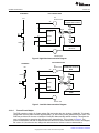
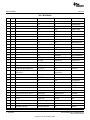
1
User's Guide
SLLU136A – September 2011 – Revised November 2012
ISO5500EVM
This document describes the ISO5500 Evaluation Module (EVM) and allows designers to analyze and
evaluate the Texas Instruments ISO5500 Isolated Gate Driver.
The ISO5500EVM can be used to evaluate device parameters while acting as a guide for board layout.
The board allows the user to evaluate device performance using a simulated (10-nF) IGBT load installed
on the board, or to install an IGBT or MOSFET (TO-247 package) onto the board and drive it with the
ISO5500.
1
2
Contents
Introduction ..................................................................................................................
1.1
Overview ............................................................................................................
1.2
ISO5500EVM Kit Contents .......................................................................................
Printed-Circuit Board .......................................................................................................
2.1
ISO5500 Operation ................................................................................................
2.2
Schematic and Bill of Materials ..................................................................................
1
1
2
2
2
5
List of Figures
1
2
3
4
........................................................................
High-Side Interconnection Diagram ......................................................................................
Low-Side Interconnection Diagram .......................................................................................
Component Changes to Change Turnon/Turnoff .......................................................................
ISO5500 Pinout and Functional Block Diagram
2
4
4
5
List of Tables
1
Test Points ................................................................................................................... 5
2
Bill of Materials .............................................................................................................. 6
1
Introduction
1.1
Overview
This ISO5500EVM was designed to allow the user to evaluate the performance and features of the
ISO5500. This includes the IGBT desaturation protection (DESAT) and the UVLO circuit that ensures a
sufficient gate voltage is available to drive the IGBT or MOSFET. The printed-circuit board (PCB) also
includes provisions to adjust the turnon/turnoff characteristics by changing the loading between the
ISO5500 output and the IGBT (or MOSFET) gate.
The EVM kit includes the ISO5500 data sheet. Figure 1 shows the device pinout and the functional block
diagram.
QuietZone is a trademark of 3M.
SLLU136A – September 2011 – Revised November 2012
Submit Documentation Feedback
Copyright © 2011–2012, Texas Instruments Incorporated
ISO5500EVM
1
Printed-Circuit Board
www.ti.com
DEVICE PINOUT
1
2
3
4
5
6
7
8
VIN+
VE
VIN-
VEE
VCC1
16
15
14
DESAT
VCC2
13
VC
12
VOUT
11
NC
VEE
10
GND1
VEE
9
GND1
RESET
FAULT
Figure 1. ISO5500 Pinout and Functional Block Diagram
1.2
ISO5500EVM Kit Contents
•
•
•
2
ISO5500EVM printed-circuit board with ISO5500DW installed (P/N 6512405)
ISO5500EVM User’s Guide (This document)
ISO5500 data sheet
Printed-Circuit Board
The ISO5500 is an isolated gate driver with several important features. The printed-circuit board (PCB)
has been designed to support this device and to allow the user to evaluate its basic operation and
features. The left side of the PCB contains the interface to the input, control, and status functions of the
integrated circuit (IC). The right side of the PCB has been designed to interface to an IGBT (or MOSFET).
No electrical connections exist between the right and left sides of the PCB.
Refer to the ISO5500EVM schematic and bill of materials to become familiar with the PCB components
and layout. The PCB files (Gerber/ODB) are available from Texas Instruments on request.
2.1
ISO5500 Operation
2.1.1
Left-Side Operation: DC Power, Control, and Status
2.1.1.1
DC Power
The left side of the ISO5500 (and therefore the PCB) can be operated using either a +3.3-V (±10%) or +5V (±10%) dc power supply. The small amount of dc current required (<20 mA) means that the device can
also be battery operated. The dc power supply must be connected to TP10 (+5 Vdc) and TP9 (+5-Vdc
return). Also, a user can solder wires directly to the PCB from the dc power supply by means of the plated
through-holes located next to the test points.
2.1.1.2
Control and Status
The interface to the device is via the JMP1 header. It contains the VIN+ and VIN– inputs, the device
RESET, and FAULT indicator output. The JMP1 header allows easy connections to test equipment using
standard clip leads or QuietZone™ connectors. Each of the four signals also has a test point for additional
connections. These are TP1 through TP4.
2
ISO5500EVM
SLLU136A – September 2011 – Revised November 2012
Submit Documentation Feedback
Copyright © 2011–2012, Texas Instruments Incorporated
Printed-Circuit Board
www.ti.com
2.1.2
Right-Side Operation
2.1.2.1
DC Power
Power is provided to Vcc2 on the right side of the device at TP12 (+Vdc) and TP11 (–Vdc). The dc supply
must be able to provide a bias voltage over the range of +15 Vdc to +30 Vdc. As the current requirement
is extremely low, the user may choose to operate the ISO5500 by battery. Solder holes are provided next
to the test points if the user chooses to hardwire these connections. If a negative gate drive is required, a
dc supply (or battery) must be connected across VE (P5 or MFG1) to VEE (MGF11 or TP11). The voltage
range must be between 0 V and 15 Vdc.
2.1.2.2
DESAT – JMP2
One of the features of the ISO5500 is the IGBT desaturation protection. JMP2 provides access to the
DESAT pin. It is a 2-pin male header, and installing a shorting jumper onto JMP2 disables the DESAT
function.
2.1.2.3
IGBT (or MOSFET)
As shipped, the ISO5500EVM does not have an IGBT installed. The user can evaluate device operation
using a simulated IGBT load or they can remove the simulated load and install an IGBT onto the board.
Most IGBTs are available in the standard TO-247 package. The PCB has provisions to solder an IGBT
directly onto the board.
2.1.2.3.1
No IGBT (or MOSFET) Installed – JMP3
When using the simulated load, the user must install a jumper short onto JMP3. This connects a 10-nF
capacitor (C9) to the Vout pin. The simulated IGBT consists of the 10-Ω gate resistor (R4) and this 10-nF
capacitor (C9).
2.1.2.3.2
IGBT (or MOSFET) Installed – REMOVE JMP3
If the user chooses to install an IGBT, JMP must be left open with no shorting jumper installed. The PCB
has been designed with several large plated-through holes (or vias) to support both high-side and low-side
drive configurations. (Note: Plated-through holes are designated as MFGx on the schematic.) The
connections for these modes are described next.
2.1.2.3.3
High-Side/Low-Side Operation and Interconnection
The connections required for high-side and low-side operation are shown in Figure 2 and Figure 3,
respectively. The user can select the load and install it directly on the PCB.
SLLU136A – September 2011 – Revised November 2012
Submit Documentation Feedback
Copyright © 2011–2012, Texas Instruments Incorporated
ISO5500EVM
3
Printed-Circuit Board
www.ti.com
SCHEMATIC
PCB CONNECTIONS
P5
Banana-Jack
+HV
+HV RETURN
CONNECTED TO MFG5
MFG5
VE
D
MFG1
MFG3
SOURCE
G
MFG2
LOAD
MFG4
DRAIN
S
MFG6
GATE
LOAD
Q1
+HV CONNECTED TO P6
OR MFG2
P6
Banana-Jack
Figure 2. High-Side Interconnection Diagram
PCB CONNECTIONS
SCHEMATIC
P5
Banana-Jack
+HV
VE
+HV RETURN
CONNECTED TO P5 OR
MFG1
MFG5
LOAD
D
MFG1
MFG3
MFG2
MFG4
SOURCE
G
DRAIN
LOAD
MFG6
GATE
S
Q1
+HV CONNECTED TO
MFG6
P6
Banana-Jack
Figure 3. Low-Side Interconnection Diagram
2.1.2.4
Turnon/Turnoff Adjust
The PCB contains a single, 10-Ω gate resistor (R4) and a short bus wire in place of diode D2. This simple
configuration sets the peak current at approximately 3 A, with turnon/ turnoff characteristics the same. The
PCB has provisions for the user to install the D2 and D3 diodes and R4 and R5 resistors. This allows the
user to evaluate device operation with different on/off characteristics. This is shown in Figure 4. The
turnon characteristics can also be adjusted with the value of R2, which connects VC to VCC2. As shipped,
R2 is set to 0 Ω, but the user can change this and examine the effects on turnon characteristics.
4
ISO5500EVM
SLLU136A – September 2011 – Revised November 2012
Submit Documentation Feedback
Copyright © 2011–2012, Texas Instruments Incorporated
Printed-Circuit Board
www.ti.com
Turnon/Turnoff The
Same
To Change Turnon and
Turnoff
R4
D2
D3
R5
R4
D2
D3
R5
(As Shipped)
Figure 4. Component Changes to Change Turnon/Turnoff
2.1.2.5
The Interchange Jumper – JMP8
The ISO5500 device is similar to other devices currently available from other manufacturers. One of the
similar devices uses pin 15 as an output driver for an LED. The TI ISO5500 uses pin 15 as a VEE (GND)
connection. If the user wishes to install a different device onto the PCB, and that device does not use pin
15 as a VEE connection, the user can simply use the jumper short from JMP8. This opens the pin 15
connection to VEE. JMP8 can then be used as a test point for the output signal on pin 15.
2.1.3
Test Points
Test points have been provided for ready access to signal monitoring. They are listed in Table 1.
Table 1. Test Points
2.2
TEST POINT
I/O
TP1
Output
TP2
TP3
FUNCTION
FAULT PIN
(Left side)
Input
RESET
(Left side)
Input
VIN–
(Left side)
TP4
Input
VIN+
(Left side)
TP5
Output
VOUT
(Right Side)
TP6
Output
GATE VOLTAGE
(Right Side)
TP7
Input
DRAIN VOLTAGE
(Right Side)
TP8
Input
DESAT VOLTAGE (Right Side)
TP9
Output
GND1
(Left side)
TP10
Input
VCC1
(Left side)
TP11
Output
VEE
(Right Side)
TP12
Input
VCC2
(Right Side)
TP13
Input
VE
(Right Side)
Schematic and Bill of Materials
The ISO5500EVM schematic follows the bill of materials.
SLLU136A – September 2011 – Revised November 2012
Submit Documentation Feedback
Copyright © 2011–2012, Texas Instruments Incorporated
ISO5500EVM
5
Printed-Circuit Board
www.ti.com
Table 2. Bill of Materials
6
Item
Qty
Reference
Value
Manufacturer
Manufacturer Part No
1
1
C1
68 µF
AVX
TPSE686K020R0150
2
1
C2
10 µF
AVX
TPSB106K020R1000
3
1
C3
1 µF
AVX
TPSA105K020R3000
4
1
C4
0.1 µF
GARRETT
X7R0805HTTD104K
5
2
C5,C13
0.01 µF
KEMET
C0805C103M5RACTU
6
1
C6
330 pF
KEMET
C0805C331J5GACTU
7
2
C7,C14
0.1 µF
KEMET
C0805C104K5RACTU
8
1
C8
100 pF
KEMET
C0805C101J5GACTU
9
1
C9
10 nF
KEMET
C0805C103K1RAC3123
10
1
C10
10 µF
TAIYO-YUDEN
UMK325BJ106MM-T
11
1
C11
1 µF
PANASONIC
ECQ-V1J105JM
12
1
C12
0.1 µF
KEMET
C0805C104M5RACTU
13
2
C15,C16
4.7 µF
VISHAY SPRAGUE
TR3D475K050C0300
14
1
C17
68 µF
United Chemicon
EMVY500ADA680MHZ0G
15
1
D1
UF4007
VISHAY
UF4007
16
1
D2
DNI - UF4007
16 AWG Wire Short
16 AWG Wire Short
17
1
D3
DNI - UF4007
VISHAY
UF4007
18
1
JMP1
HDR_THVT_2x4_100M
Sullins
S1032-04-ND
19
7
JMP2,JMP3,JMP4,JMP5,JMP6,JMP7,JMP8
HDR_THVT_1x2
Sullins
S1032-02-ND
20
10
MFG1,MFG2,MFG3,MFG4,MFG5,MFG6,MFG9,MFG
10,MFG11,MFG12
MFG060_PTH
Plated Through Holes 0.060" Holes for
Customer Use Only
21
2
P5,P6
Banana-Jack
ITT-POMONA
3267
22
1
Q1
POWER FET
DNI
DNI
23
1
R1
3.3K
VISHAY
CRCW0805332FKEF
24
1
R2
0
Panasonic
ERJ-6GEY0R00V
25
1
R3
100
Panasonic
ERJ-6GEY101V
26
1
R4
10
Panasonic
ERJ-1TYF100U
27
1
R5
DNI - 10
Panasonic
ERJ-1TYF100U
28
9
TP1,TP2,TP3,TP4,TP5,TP6,TP7,TP8,TP13
Test Loop - Black
Component Corporation
TP-105-40-00
29
2
TP9,TP11
Test Loop - Black
KEYSTONE
5011
30
2
TP10,TP12
Test Loop - RED
KEYSTONE
5010
31
1
U1
ISO5500
Texas Instruments
ISO5500
32
4
Bottom Side as shown on Bottom Side Silkscreen
Bumpon Hemisphere - Black
3M
SJ-5003
33
5
To Be Installed on JMP4–JMP7
Jumper Shorts With Handle
TYCO
2-881545-2
ISO5500EVM
SLLU136A – September 2011 – Revised November 2012
Submit Documentation Feedback
Copyright © 2011–2012, Texas Instruments Incorporated
Printed-Circuit Board
www.ti.com
Table 2. Bill of Materials (continued)
Item
Qty
Reference
Value
Manufacturer
Manufacturer Part No
NOTE ASSEMBLY INSTRUCTIONS BELOW:
INSTALL JUMPER SHORTS (ITEM 33) ONTO THE FOLLOWING JUMPER LOCATIONS:
JMP1-3 TO JMP1-4
JMP1-5 TO JMP1-6
JMP2
JMP8
JMP9
INSTALL #16AWG WIRE IN PLACE OF D2
SLLU136A – September 2011 – Revised November 2012
Submit Documentation Feedback
ISO5500EVM
Copyright © 2011–2012, Texas Instruments Incorporated
7
Printed-Circuit Board
www.ti.com
SPACER - TO DELETE BLANK PAGE BEFORE THE IMPORTANT NOTICE
8
ISO5500EVM
SLLU136A – September 2011 – Revised November 2012
Submit Documentation Feedback
Copyright © 2011–2012, Texas Instruments Incorporated
Evaluation Board/Kit Important Notice
Texas Instruments (TI) provides the enclosed product(s) under the following conditions:
This evaluation board/kit is intended for use for ENGINEERING DEVELOPMENT, DEMONSTRATION, OR EVALUATION PURPOSES
ONLY and is not considered by TI to be a finished end-product fit for general consumer use. Persons handling the product(s) must have
electronics training and observe good engineering practice standards. As such, the goods being provided are not intended to be complete
in terms of required design-, marketing-, and/or manufacturing-related protective considerations, including product safety and environmental
measures typically found in end products that incorporate such semiconductor components or circuit boards. This evaluation board/kit does
not fall within the scope of the European Union directives regarding electromagnetic compatibility, restricted substances (RoHS), recycling
(WEEE), FCC, CE or UL, and therefore may not meet the technical requirements of these directives or other related directives.
Should this evaluation board/kit not meet the specifications indicated in the User’s Guide, the board/kit may be returned within 30 days from
the date of delivery for a full refund. THE FOREGOING WARRANTY IS THE EXCLUSIVE WARRANTY MADE BY SELLER TO BUYER
AND IS IN LIEU OF ALL OTHER WARRANTIES, EXPRESSED, IMPLIED, OR STATUTORY, INCLUDING ANY WARRANTY OF
MERCHANTABILITY OR FITNESS FOR ANY PARTICULAR PURPOSE.
The user assumes all responsibility and liability for proper and safe handling of the goods. Further, the user indemnifies TI from all claims
arising from the handling or use of the goods. Due to the open construction of the product, it is the user’s responsibility to take any and all
appropriate precautions with regard to electrostatic discharge.
EXCEPT TO THE EXTENT OF THE INDEMNITY SET FORTH ABOVE, NEITHER PARTY SHALL BE LIABLE TO THE OTHER FOR ANY
INDIRECT, SPECIAL, INCIDENTAL, OR CONSEQUENTIAL DAMAGES.
TI currently deals with a variety of customers for products, and therefore our arrangement with the user is not exclusive.
TI assumes no liability for applications assistance, customer product design, software performance, or infringement of patents or
services described herein.
Please read the User’s Guide and, specifically, the Warnings and Restrictions notice in the User’s Guide prior to handling the product. This
notice contains important safety information about temperatures and voltages. For additional information on TI’s environmental and/or
safety programs, please contact the TI application engineer or visit www.ti.com/esh.
No license is granted under any patent right or other intellectual property right of TI covering or relating to any machine, process, or
combination in which such TI products or services might be or are used.
FCC Warning
This evaluation board/kit is intended for use for ENGINEERING DEVELOPMENT, DEMONSTRATION, OR EVALUATION PURPOSES
ONLY and is not considered by TI to be a finished end-product fit for general consumer use. It generates, uses, and can radiate radio
frequency energy and has not been tested for compliance with the limits of computing devices pursuant to part 15 of FCC rules, which are
designed to provide reasonable protection against radio frequency interference. Operation of this equipment in other environments may
cause interference with radio communications, in which case the user at his own expense will be required to take whatever measures may
be required to correct this interference.
EVM Warnings and Restrictions
It is important to operate this EVM within the input voltage range of 3.3 V to 5 V and the output voltage range of 10 V to 30 V .
Exceeding the specified input range may cause unexpected operation and/or irreversible damage to the EVM. If there are questions
concerning the input range, please contact a TI field representative prior to connecting the input power.
Applying loads outside of the specified output range may result in unintended operation and/or possible permanent damage to the EVM.
Please consult the EVM User's Guide prior to connecting any load to the EVM output. If there is uncertainty as to the load specification,
please contact a TI field representative.
During normal operation, some circuit components may have case temperatures greater than 80° C. The EVM is designed to operate
properly with certain components above 80° C as long as the input and output ranges are maintained. These components include but are
not limited to linear regulators, switching transistors, pass transistors, and current sense resistors. These types of devices can be identified
using the EVM schematic located in the EVM User's Guide. When placing measurement probes near these devices during operation,
please be aware that these devices may be very warm to the touch.
Mailing Address: Texas Instruments, Post Office Box 655303, Dallas, Texas 75265
Copyright © 2012, Texas Instruments Incorporated
IMPORTANT NOTICE
Texas Instruments Incorporated and its subsidiaries (TI) reserve the right to make corrections, enhancements, improvements and other
changes to its semiconductor products and services per JESD46, latest issue, and to discontinue any product or service per JESD48, latest
issue. Buyers should obtain the latest relevant information before placing orders and should verify that such information is current and
complete. All semiconductor products (also referred to herein as “components”) are sold subject to TI’s terms and conditions of sale
supplied at the time of order acknowledgment.
TI warrants performance of its components to the specifications applicable at the time of sale, in accordance with the warranty in TI’s terms
and conditions of sale of semiconductor products. Testing and other quality control techniques are used to the extent TI deems necessary
to support this warranty. Except where mandated by applicable law, testing of all parameters of each component is not necessarily
performed.
TI assumes no liability for applications assistance or the design of Buyers’ products. Buyers are responsible for their products and
applications using TI components. To minimize the risks associated with Buyers’ products and applications, Buyers should provide
adequate design and operating safeguards.
TI does not warrant or represent that any license, either express or implied, is granted under any patent right, copyright, mask work right, or
other intellectual property right relating to any combination, machine, or process in which TI components or services are used. Information
published by TI regarding third-party products or services does not constitute a license to use such products or services or a warranty or
endorsement thereof. Use of such information may require a license from a third party under the patents or other intellectual property of the
third party, or a license from TI under the patents or other intellectual property of TI.
Reproduction of significant portions of TI information in TI data books or data sheets is permissible only if reproduction is without alteration
and is accompanied by all associated warranties, conditions, limitations, and notices. TI is not responsible or liable for such altered
documentation. Information of third parties may be subject to additional restrictions.
Resale of TI components or services with statements different from or beyond the parameters stated by TI for that component or service
voids all express and any implied warranties for the associated TI component or service and is an unfair and deceptive business practice.
TI is not responsible or liable for any such statements.
Buyer acknowledges and agrees that it is solely responsible for compliance with all legal, regulatory and safety-related requirements
concerning its products, and any use of TI components in its applications, notwithstanding any applications-related information or support
that may be provided by TI. Buyer represents and agrees that it has all the necessary expertise to create and implement safeguards which
anticipate dangerous consequences of failures, monitor failures and their consequences, lessen the likelihood of failures that might cause
harm and take appropriate remedial actions. Buyer will fully indemnify TI and its representatives against any damages arising out of the use
of any TI components in safety-critical applications.
In some cases, TI components may be promoted specifically to facilitate safety-related applications. With such components, TI’s goal is to
help enable customers to design and create their own end-product solutions that meet applicable functional safety standards and
requirements. Nonetheless, such components are subject to these terms.
No TI components are authorized for use in FDA Class III (or similar life-critical medical equipment) unless authorized officers of the parties
have executed a special agreement specifically governing such use.
Only those TI components which TI has specifically designated as military grade or “enhanced plastic” are designed and intended for use in
military/aerospace applications or environments. Buyer acknowledges and agrees that any military or aerospace use of TI components
which have not been so designated is solely at the Buyer's risk, and that Buyer is solely responsible for compliance with all legal and
regulatory requirements in connection with such use.
TI has specifically designated certain components which meet ISO/TS16949 requirements, mainly for automotive use. Components which
have not been so designated are neither designed nor intended for automotive use; and TI will not be responsible for any failure of such
components to meet such requirements.
Products
Applications
Audio
www.ti.com/audio
Automotive and Transportation
www.ti.com/automotive
Amplifiers
amplifier.ti.com
Communications and Telecom
www.ti.com/communications
Data Converters
dataconverter.ti.com
Computers and Peripherals
www.ti.com/computers
DLP® Products
www.dlp.com
Consumer Electronics
www.ti.com/consumer-apps
DSP
dsp.ti.com
Energy and Lighting
www.ti.com/energy
Clocks and Timers
www.ti.com/clocks
Industrial
www.ti.com/industrial
Interface
interface.ti.com
Medical
www.ti.com/medical
Logic
logic.ti.com
Security
www.ti.com/security
Power Mgmt
power.ti.com
Space, Avionics and Defense
www.ti.com/space-avionics-defense
Microcontrollers
microcontroller.ti.com
Video and Imaging
www.ti.com/video
RFID
www.ti-rfid.com
OMAP Applications Processors
www.ti.com/omap
TI E2E Community
e2e.ti.com
Wireless Connectivity
www.ti.com/wirelessconnectivity
Mailing Address: Texas Instruments, Post Office Box 655303, Dallas, Texas 75265
Copyright © 2012, Texas Instruments Incorporated