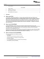
1
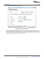
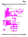
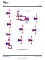
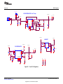
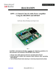
User's Guide
SLLU225 – August 2015
DP159RGZ Evaluation Module
This document describes how to use and configure the DP159RGZEVM along with recommendations for
system hardware implementation. These recommendations are only guidelines and it is the designer’s
responsibility to consider all system characteristics and requirements. Engineers should refer to the
datasheet for technical details such as device operation, terminal description, and so forth.
1
2
3
4
5
6
7
Contents
Overview ...................................................................................................................... 2
1.1
What is the DP159? ................................................................................................ 2
1.2
What is the DP159RGZEVM?..................................................................................... 2
1.3
What is Included in the DP159RGZEVM? ....................................................................... 2
1.4
DP159RGZEVM Board ............................................................................................ 3
Hardware Description ....................................................................................................... 3
2.1
Video Connectors for DP159 Ports ............................................................................... 4
2.2
Enable/Reset ........................................................................................................ 4
2.3
Power ................................................................................................................. 4
2.4
Jumper Configuration .............................................................................................. 5
2.5
Component Population Configuration ............................................................................ 6
2.6
Local I2C Access Through J5 ..................................................................................... 7
2.7
Local I2C Access Through USB Interface via TUSB3410 .................................................... 7
2.8
Rsadj Potentiometer ................................................................................................ 9
Quick Start Guide ............................................................................................................ 9
References ................................................................................................................... 9
EVM Bill of Materials ....................................................................................................... 10
EVM Schematics .......................................................................................................... 12
EVM Layout ................................................................................................................. 19
List of Figures
.....................................................................................................
1
DP159RGZEVM Board
2
DP159RGZEVM Block Diagram ........................................................................................... 3
3
Register Status / Control Tab .............................................................................................. 8
4
Eye Scan Tab ................................................................................................................ 9
5
HDMI Input Connectors
6
DP159RGZ .................................................................................................................. 13
7
HDMI TX Connector
8
9
10
11
12
13
14
15
16
...................................................................................................
.......................................................................................................
DP159RGZEVM Select Options..........................................................................................
Reset ........................................................................................................................
1.1- and 3.3-V Regulators ................................................................................................
TUSB3410...................................................................................................................
Layer 1 (Top) ...............................................................................................................
Layer 2 (GND) ..............................................................................................................
Layer 3 (Power) ............................................................................................................
Layer 4 (Power) ............................................................................................................
Layer 5 (GND) ..............................................................................................................
3
12
14
15
16
17
18
19
19
20
20
21
I2C is a trademark of NXP.
All other trademarks are the property of their respective owners.
SLLU225 – August 2015
Submit Documentation Feedback
DP159RGZ Evaluation Module
Copyright © 2015, Texas Instruments Incorporated
1
Overview
17
www.ti.com
Layer 6 (Bottom)............................................................................................................ 21
List of Tables
1
Jumper Settings .............................................................................................................. 5
2
Aardvark I2C (J5) Pin-Out ................................................................................................... 7
3
DP159 Target I2C Address
4
................................................................................................. 7
DP159RGZEVM Bill of Materials ......................................................................................... 10
1
Overview
1.1
What is the DP159?
The DP159 is a Dual-Mode DisplayPort to Transition Minimized Differential Signal (TMDS) retimer
supporting Digital Video Interface (DVI) 1.0 and High Definition Multimedia Interface (HDMI) 1.4b and 2.0
output signals. The DP159 supports the Dual-Mode Standard version 1.1 type 1 and type 2 through the
DDC link. The DP159 supports data rates up to 6 Gbps per data lane to support UltraHD (4K x 2K / 60
Hz) 8 bits per color high resolution video and HDTV with 16-bit color depth at 1080p (1920 x 1080 / 60
Hz). The DP159 can automatically configure itself as a redriver at data rates < 1.0 Gbps or as a retimer
above this data rate.
1.2
What is the DP159RGZEVM?
The DP159RGZEVM is a PCB created to help customers evaluate the DP159 device for video
applications. This EVM can also be used as a hardware reference design for implementation of the DP159
in the RSB package. PCB design/layout files can be provided upon request to provide PCB design
illustrations of the routing/placement rules.
Please note that the EVM design supports both the standard DP159 application and a DP159-thru-HDMI
application, so it contains many components that would not be needed by a typical DP159 application. A
separate reference design specific to the DP159 is available for customers.
1.3
What is Included in the DP159RGZEVM?
The major components of the EVM are as follows:
• DP159RGZ
• Standard DP sink connector (connects to source)
• Standard HDMI source connector (connects to sink)
• DC power regulators
• I2C™ programming interface for external I2C host connection
• USB interface (I2C utility available)
2
DP159RGZ Evaluation Module
SLLU225 – August 2015
Submit Documentation Feedback
Copyright © 2015, Texas Instruments Incorporated
Overview
www.ti.com
1.4
DP159RGZEVM Board
Figure 1 illustrates the DP159RGZEVM board.
Figure 1. DP159RGZEVM Board
2
Hardware Description
Figure 2 shows the DP159RGZEVM block diagram.
USB2
Connector
5-V
DONGLE
5-V to 3.3-V
LDO
AARDVARK
Connector
TUSB3410
3.3-V to 1.1-V
LDO
SCL_CTL
TMDS_D2P/N
IN0P/N
TMDS_D1P/N
IN1P/N
IN2P/N
DP159
(48-pin QFN)
TMDS_D0P/N
IN3P/N
TMDS_CLKP/N
AUXP/N
DDC_SCL/SDA
HDMI Connector
DP Connector Top
SDA_CTL
DDC - Snoop Only
100-Ω differential impedance for HDMI differential pairs.
Figure 2. DP159RGZEVM Block Diagram
SLLU225 – August 2015
Submit Documentation Feedback
DP159RGZ Evaluation Module
Copyright © 2015, Texas Instruments Incorporated
3
Hardware Description
2.1
www.ti.com
Video Connectors for DP159 Ports
The EVM has a DP connection for the source and a HDMI connection for the sink. J2 is a standard DP
connector (Molex 47272-0001). P2 is a standard HDMI connector (Molex 4715-10001). There is a third
video connection on the board for a HDMI source (P1), this function is not installed on the
DP159RGZEVM.
2.2
Enable/Reset
There are three device enable/reset options to use with the EVM:
(A) Supervisor circuitry option
This is the default configuration on the DP159RGZEVM. The enable (EN) signal is held low until the
power good (PG) from the 3.3-V voltage regulator reaches a stable high-voltage level then released
high.
(B) RC timing option
C26 external capacitor and internal resistor are used to control the EN ramp time after the device is
powered on. C26 is a Do Not Install (DNI option) by default. C26 needs to be installed and R77 needs
to be uninstalled to enable this option.
(C) External control option
A push button (SW1) is provided for manual control of the DP159’s EN/OE input.
2.3
Power
A DC power jack (J9) to accept a 5-V wall power adapter is provided on the EVM. The DC power jack
(CUI Inc. PJ-202AH) has an inner diameter of 2.1 mm and an outer diameter of 5.5 mm. The tip of the +5V power supply must be positive. A +5-V power supply of at least 1.5 A that meets the given requirements
can be used to power the DP159RGZEVM. Power is provided to the EVM from the 5-V wall power
adapter when SW2 is set to position 1.
CAUTION
Care should be taken to not plug in any power source higher than the
configured voltage (5 V).
Alternately, it is possible to power the EVM by connecting a USB Micro cable from J13 to a USB host and
setting SW2 to position 3.
4
DP159RGZ Evaluation Module
SLLU225 – August 2015
Submit Documentation Feedback
Copyright © 2015, Texas Instruments Incorporated
Hardware Description
www.ti.com
2.4
Jumper Configuration
Jumpers are provided to operate the device/EVM in different configurations. Table 1 lists the jumper
settings.
Table 1. Jumper Settings
Jumper
Signal Name
Description
Default Config
J1
HPD_SRC
JP 1-2 for DP159 thru HDMI
NC
JP 2-3 for NOT USED
NC for DP159
J3
I2_EN_PIN
JP 1-2 for I2C ENABLE
JP 2-3 for PIN STRAP
NC: Enables device configuration from I2C
or pin straps.
NC – PIN STRAP (internal pulldown)
J4
SCL
JP 1-2 for USB IF TO I2C
JP 1-2: USB I2C Interface
2
JP 2-3 for EXT IF TO I C
NC – N/A
J6
SDA
JP 1-2 for USB IF TO I2C
JP 1-2: USB I2C Interface
2
JP 2-3 for EXT IF TO I C
NC – N/A
J7
HDMI_SEL_TEST_A1
JP 1-2 for:
NC
2
• I C Addr bit A1 = 1, when I2C_EN = H
• DVI mode, when I2C_EN = L
JP 2-3 for:
• I2C Addr bit A1 = 0, when I2C_EN = H
• Normal mode, when I2C_EN = L
NC for weak internal pulldown (HDMI
mode)
J8
VSADJ
JP 1-2 for 7.0 kΩ
JP 1-2: Default of 7.0 kΩ
JP 2-3 for adjustable resistance
NC – N/A
J10
SLEW_CTL
JP 1-2 for fastest data rate
NC
JP 2-3 for 20 ps slow
NC for 40 ps slow
J11
SIG_EN
JP 1-2 for Signal Detect Enabled
NC
JP 2-3 for Signal Detect Disabled
NC for weak internal pullup (Detect
Disabled)
J12
EQ_SEL_A0
JP 1-2 for:
NC
• I2C Addr bit A0 = 1, when I2C_EN = H
• Fixed EQ at 14 dB, when I2C_EN = L
JP 2-3 for:
• I2C Addr bit A0 = 0, when I2C_EN = H
• Fixed EQ at 7.5 dB, when I2C_EN = L
NC for adaptive EQ
J14
TX_TERM_CTL
JP 1-2 for No TX termination
NC
JP 2-3 for TX termination 75–100 Ω
NC for auto termination set
J15
PRE_SEL
JP 1-2 for –5 dB
NC
JP 2-3 for –2.5 dB
NC for 0 dB
SLLU225 – August 2015
Submit Documentation Feedback
DP159RGZ Evaluation Module
Copyright © 2015, Texas Instruments Incorporated
5
Hardware Description
www.ti.com
Table 1. Jumper Settings (continued)
Jumper
Signal Name
Description
Default Config
J16
CEC_EN
JP 1-2 for DP159 thru HDMI
NC
JP 2-3 for NOT USED
NC for DP159
J17
SWAP/POL
JP 1-2 for Polarity Swap
NC
JP 2-3 for Lane Swap
NC for No Swap
2.5
Component Population Configuration
To allow the DP159RGZEVM to support both the default DP input as well as a HDMI test input, there are
many components that need to be removed, placed, or modified depending on the board configuration.
Here’s a summary of the default component configuration for the DP159RGZEVM. In addition, the unused
HDMI receptacle is depopulated.
Function
Differential Pair - IN
Differential Pair - HDMI IN
SDA / SCL - HDMI
Differential Pair - DP IN
SDA / SCL / HPD - DP
Pullup Differential Pair HDMI IN
2.5.1
Reference Designator
C11, C12, C13, C14, C15, C16, C24,
C25
R14, R15, R18, R19, R20, R21, R22,
R23
R16, R17, R24, R25, R123, R124
R112, R109, R111, R108, R110, R107,
R106, R105
R33, R31, R32 (R126, R135, R132,
R133 - snoop)
R1, R2, R3, R4, R6, R7, R8, R9
DP159RGZEVM
populated with 0.1 µF
not populated
not populated
populated with 0 Ω
populated with 0 Ω
populated, but not
connected
HPD Snoop Option
To accommodate systems that do not properly resend DDC commands after HPD goes low, we have
implemented a HPD snoop mode on the DP159RGZEVM. This mode allows the HPD line to be routed
around the DP159, but remain connected to the DP159 on the sink side to allow the DP159 to snoop its
state. This snoop mode is disabled by default on the DP159RGZEVMs.
• Pop R131, no pop R129, R130, R139 for HPD on
• No pop R131, pop R129, R130, R139 for HPD snoop only
2.5.2
DDC Snoop Option – not Available for DP159RGZ REV B
To accommodate systems that do not properly support clock stretching on the DDC lines, we have
implemented a snoop mode on the DP159RGZEVM. This mode allows the DDC lines to be routed around
the DP159RGZ, but remain connected to the DP159RGZ on the sink side to allow the DP159RGZ to
snoop the DDC traffic. This snoop mode is enabled by default on the DP159RGZ REV B1 EVMs.
• Pop R126, R125, R132, R133. No pop R31, R32 – DP159RGZ, DDC snoop only
• Pop R31, R32. No pop R126, R125, R132, R133 – DP159RGZ, DDC on
6
DP159RGZ Evaluation Module
SLLU225 – August 2015
Submit Documentation Feedback
Copyright © 2015, Texas Instruments Incorporated
Hardware Description
www.ti.com
2.6
2
Local I C Access Through J5
Access to DP159’s local I2C signals is provided via the J5 input connector. Note that I2C signal levels
should be at 3.3 V when I2C interface is accessed through the connector.
A standalone external I2C host can be connected via J5 for debug and control purposes. An example of an
external I2C Host controller is the Total Phase Aardvark I2C/SPI Host Adapter (Total Phase Part#:
TP240141). Sample scripts for this I2C Host controller are provided by request.
Table 2. Aardvark I2C (J5) Pin-Out
J5 pin #
Description
J5 pin
#
Description
1
SCL_CTL
2
GND
3
SDA_CTL
4
NC
5
NC
6
NC
7
NC
8
NC
9
NC
10
GND
Table 3. DP159 Target I2C Address (1)
DP159 I2C Target Address
Bit 7 (MSB)
Bit 6
Bit 5
Bit 4
Bit 3
Bit 2
Bit 1
A6
A5
A4
A3
A2
A1
A0
0
1
1
1
1
0
1
(1)
2.7
Bit 0 (W/R)
0/1
2
The target I C address for DP159 can be modified by the EVM jumper settings.
Local I2C Access Through USB Interface via TUSB3410
Access to DP159’s local I2C signals is also provided through the TUSB3410 on the DP159RGZEVM using
a USB TI Utility called Eye Scan. To use the utility:
• Install the Eye Scan software from Texas Instruments
• J6 must be set to SDA – SDA_USB
• J4 must be set to SCL – SCL_USB
• Attach USB micro cable to J13 and to the host computer
NOTE: The USB connection should be made prior to installing any DP or HDMI cables.
•
Start the Eye Scan software
SLLU225 – August 2015
Submit Documentation Feedback
DP159RGZ Evaluation Module
Copyright © 2015, Texas Instruments Incorporated
7
Hardware Description
www.ti.com
Figure 3 shows the Register Status / Control tab.
Figure 3. Register Status / Control Tab
Confirm that the SN65DP149/159/TMDS171/181 Interface is present and selected at the top. If it is not,
check the USB connection and confirm that the driver is loaded in Device Manager. It may take a moment
for the USB driver to load, if the DP159RGZ does not appear, hit the Refresh button. This tab can be used
to read and write the status and control registers of the device.
8
DP159RGZ Evaluation Module
SLLU225 – August 2015
Submit Documentation Feedback
Copyright © 2015, Texas Instruments Incorporated
Hardware Description
www.ti.com
Figure 4 shows the Eye Scan tab.
Figure 4. Eye Scan Tab
To run an Eye Scan, select the Eye Scan tab, select the relevant lanes, and press scan. Please note that
Eye Scan cannot be performed when the device is in retimer mode, it does not function in redriver mode.
2.8
Rsadj Potentiometer
The default Rsadj value on the DP159RGZEVM is 7.0 kΩ. The optimal value for an application may vary
from 4.7 kΩ to 7 kΩ. To allow customers to test the effects of various Rsadj values, there is a
potentiometer on the EVM at R76. The Rsadj value can be varied by turning the knob and setting J8 to
[2,3].
3
Quick Start Guide
The following steps provide quick start instructions:
1. Connect USB cable from J13 to a USB host, set SW2 to 3. LED D2 should light up.
Option: Apply 5-V power to J9, set SW2 to 1. LED D2 should light up.
2. If using external I2C adapter instead of pin straps, please configure the DP159 at this step using J5 or
through the USB interface.
3. Plug in a DP source using a standard DP cable into J2 (Standard DP connector).
4. Plug in an HDMI video sink device into P2 (standard HDMI connector) using a standard HDMI cable.
5. Video output on HDMI sink should be observed.
4
References
1.
2.
3.
4.
DP159 Data Sheet
Aardvark Adapter User Manual
High-Definition Multimedia Interface Specification Version 1.4b.
High-Definition Multimedia Interface Specification Version 2.0.
SLLU225 – August 2015
Submit Documentation Feedback
DP159RGZ Evaluation Module
Copyright © 2015, Texas Instruments Incorporated
9
EVM Bill of Materials
5
www.ti.com
EVM Bill of Materials
Table 4 lists the DP159RGZEVM BOM.
Table 4. DP159RGZEVM Bill of Materials
10
Item
Qty
Reference
Part
PCB Footprint
Manufacturer
Part Number
1
2
C1,C52
1 uF
603
Taiyo Yuden
LMK107B7105KA-T
2
12
C9,C10,C17,C18,C19,C21,C
23,C29,C40,C46,C59,C60
0.1uF
402
Yageo
CC0402KRX5R6BB104
3
5
C8,C20,C35,C36,C57
10uF
805
TDK
C2012X5R1A106K125AB
68
1
C31
10uF
805
TDK
C2012X5R1C106K085AC
4
8
C11,C12,C13,C14,C15,C16,
C24,C25
0.1uF
201
TDK
C0603X5R0J104M
5
5
C22,C37,C41,C42,C47
0.01uF
402
6
1
C26 - DNI
DNI_200nF
402
7
1
C27
18pF
402
AVX
04025A180JAT2A
8
1
C28
220pF
402
9
1
C30
220uF
7343
Kemet
T491D227K016AT
10
1
C34
3.3 nF
402
11
1
C32
22uF
805
12
2
C39,C58
2.2uF
805
13
35
C2,C3,C4,C5,C6,C7,C38,R14 DNI
,R15,R16,R17,R18,R19,R20,
R21,R22,R23,R24,R25,R35,
R87,R92,R93,R104,R113,R1
14,
R120,R123,R124,R125,R126,
R129,R130,R132, R133
402 / 201
14
2
C45,C49
22pF
402
15
2
C50,C51
33pF
402
16
1
D1
Zener 6V
SOT23
Diodes Inc.
MMBZ5233B-FDICT-ND
17
1
D2
LED Green 0805
805
Lite On
LTST-C171GKT
18
1
JP1
JUMPER
HDR_THVT_1x2_100
19
13
J1,J3,J4,J6,J7,J8,J10,J11,J1
2,J14,J15,J16,J17
HDR3X1 M .1
HDR_THVT_1x3_100
3M
961103-6404-AR
20
1
J2
Display_Port_Conne DISPLAYPORT
ctor_Sink_0
Molex
47272-0001
21
1
J5
Header 5x2 0.1"
thru-hole
con_thvt_shrd_2x5_100_m
3M
N2510-6002-RB
22
1
J9
2.1mm x 5.5mm
PJ-202AH
CUI Inc.
PJ-202AH (PJ-002AH)
23
1
J13
USB Micro B
USB Micro B
FCI
10103592-0001LF
24
17
LP1,LP2,LP3,LP4,LP5,LP6,L
P7,LP8,LP9,LP10,LP11,LP12
,LP13,LP14,LP15,LP16,LP17
LP
TESTLOOP
KOBIKONN
151-103-RC
25
1
L1
2.2 uH
1008
TDK
VLS252010ET-2R2M
26
1
L2
1 uH
1008
TDK
NLCV25T-1R0M-EFR
27
4
L3, L4, L5, L6
CHOKE
805
Murata
DLW21SN900HQ2L
28
1
P1 - DNI
HDMI_IN
CON_HDMI_RT_19_0p50mm
Molex
471510001
29
1
P2
HDMI_OUT
CON_HDMI_RT_19_0p50mm
Molex
471510001
30
2
Q1,Q2
FDV301N_NFET_8
V
SOT23
Fairchild
Semiconductor
FD301N
31
8
R1,R2,R3,R4,R6,R7,R8,R9
50
201
32
1
R5
100
402
33
6
R10,R11,R99,R100,R101,R1
21
1K
402
34
3
R12,R27,R81
100K
402
35
1
R13
10
402
36
12
R31,R32,R33,R34,R105,R10 0
6,R107,R108,R109,R110,R11
1,R112
201
DP159RGZ Evaluation Module
SLLU225 – August 2015
Submit Documentation Feedback
Copyright © 2015, Texas Instruments Incorporated
EVM Bill of Materials
www.ti.com
Table 4. DP159RGZEVM Bill of Materials (continued)
Item
Qty
Reference
Part
PCB Footprint
37
6
R28,R29,R58,R59,R45,R46
2K
402
Manufacturer
Part Number
38
7
R77,R80,R83,R84,R89,R122,
R131
0
402
39
1
R30
1M
402
40
1
R127
500K
402
41
1
R36
75
402
42
1
R56
27K
402
43
16
R57,R60,R61,R62,R63,R64,
R65,R66,R67,R68,R69,R70,
R71,R72,R73,R74
65K
402
44
1
R75
7.06K (6.98K OK)
402
45
1
R76
PTV09 10K POT
THRUHOLE
46
3
R78,R98,R102
10K
402
BOURNS
PTV09A-4015F-B103
47
2
R79,R88
4.7K
402
48
1
R82
500
402
49
1
R85
750K
402
50
1
R86
240K
402
51
1
R90
1.87K
402
52
1
R91
4.99K
402
53
1
R94
1.5K
402
54
2
R95,R96
33
201
55
1
R103
15K
402
56
1
R115
47K
402
57
1
SW1
PB_SWITCH
58
1
SW2
3POS_SPDT
SW_MOM_2NO
OMRON
B3SN-3012P
THRUHOLE_3POS
NKK Switches
59
1
U1
MS13ANW03
DP159RGZ
48_RGZ
TI
60
1
61
1
U9
SN74AUP1G04
DCK
TI
SN74AUP1G04DCKR
U2
SN74CBT1G125
DCK
TI
62
SN74CBT1G125DCKR
1
U3
TPS3808G30DBVT
6DBV
TI
TPS3808G30DBVT
63
1
U4
TPS62150A
RGT16
TI
TPS62150ARGTT
64
1
U6
TPS61240
6DRV
TI
TPS61240DRVT
65
1
U5
TPS74201RGWT
RGW20
TI
TPS74201RGWT
66
1
U7
TUSB3410
LQFP32
TI
TUSB3410VF
67
1
U8
24LC256
8SOIC
ON
Semiconductor
CAT24C256W
69
1
Y1
12 MHz Crystal
ECX-32
ECS Inc.
ECS-120-20-33-TR
70
1
U16
TPD2E001
drl_5pin
TI
TPD2E001
SLLU225 – August 2015
Submit Documentation Feedback
DP159RGZ Evaluation Module
Copyright © 2015, Texas Instruments Incorporated
11
EVM Schematics
6
www.ti.com
EVM Schematics
Figure 5 through Figure 11 show the DP159RGZEVM schematics.
BOARD_3P3V
BOARD_5V
20
21
Case1
Case2
P1
1
2
3
4
5
6
7
8
9
10
11
12
13
14
15
16
17
18
19
1
2
3
4
5
6
7
8
9
10
11
12
13
14
15
16
17
18
19
R7
50
0201
5%
R8
50
0201
5%
Pop 0 ohm series on IN_Dxx lines for DP159 thru HDMI
No pop 0 ohm series on IN_Dxx lines for DP159
No pop R104 if U6 is pop - DP159 thru HDMI
R4
50
0201
5%
BOARD_5V
R9
50
0201
5%
R10
1K
0402
J1
0
R15
0
0
R18
R19
0
0
R20
R21
0
0
R22
R23
0
IN_D2P
PAGE2,3
IN_D2N
IN_D1P
PAGE2,3
PAGE2,3
IN_D1N
IN_D0P
PAGE2,3
PAGE2,3
IN_D0N
IN_CLKP
PAGE2,3
PAGE2,3
IN_CLKN
PAGE2,3
R16
2K
0402
5%
LP15
R24
R25
HDMI_IN_5V
HPD_SRC_HDMI_RX_CONN
R104
HDR3X1 M .1
HPD_SRC
R17
2K
0402 PAGE4 HPD_SRC_CONN
5%
HPD_SRC
R11
1K
0402
R13
10
0402
1 HPD_SRC
2 HPD_SRC_HDMI_RX_CONN
3 HPD_SRC_CONN
R14
HDMI_CEC_SRC
ARC_OUT
HDMI_SCL_SRC_IN
HDMI_SDA_SRC_IN
PAGE3
R12
100K
0402
Q1
3
Q2
1
3
2
1
2
D1
Zener 6V
LP16
FDV301N_NFET_8V
FDV301N_NFET_8V
LP17
0
0
SCL_SRC
SDA_SRC
0
R126
0
R124 R123
0
0
HDMI_IN
HDMI_IN
R125
0
PAGE2,3
PAGE2,3
No pop R16, R17, R24, R25, R123, R124, R125, R126 for DP159, DDC on
Pop R126, R125. No pop R16, R17, R24, R25, R123, R124 for DP159, DDC snoop only
Pop R16, R17, R24, R25, no pop R123, R124, R125, R126 for DP159 thru HDMI, DDC on
No pop R16, R17, R24, R25. Pop R123, R124, R125, R126 for DP159 thru HDMI, DDC snoop only
HDMI_SCL_SRC
HDMI_SDA_SRC
DisplayPort++
R5
100
0402
JP 1-2 for DP159 thru HDMI
JP 2-3 NOT USED
NC for DP159
2
R6
50
0201
5%
R3
50
0201
5%
3
Case3
Case4
22
23
HDMI RX
R2
50
0201
5%
1
R1
50
0201
5%
PAGE2,3
PAGE2,3
Pop 0 ohm series on IN_Dxx lines for DP159
No pop 0 ohm series on IN_Dxx lines for DP159 thru HDMI
BOARD_3P3V
J2
DPRX_GND
C1
R30
1M
0402
5%
1 uF
21
22
23
24
GND7
GND8
GND9
GND10
ML_3n
GND1
ML_3p
ML_2n
GND2
ML_2p
ML_1n
GND3
ML_1p
ML_0n
GND4
ML_0p
CAD (GND)
DP_CEC (GND)
AUX_p (SCL)
GND6
AUX_n (SDA)
HPD
DP_PWR_RTN
DP_PWR
1
2
3
4
5
6
7
8
9
10
11
12
13
14
15
16
17
18
19
20
Display_Port_Connector_Sink_0
DISPLAYPORT IN
C_DPRX_LN3N
C_DPRX_LN3P
C_DPRX_LN2N
C_DPRX_LN2P
C_DPRX_LN1N
C_DPRX_LN1P
R112
0
R109
0
R111
0
R108
0
R110
0
0
R106
0
R107
C_DPRX_LN0N
C_DPRX_LN0P
DP_CAD
CEC_SRC
DP_SCL_SRC
R105
0
IN_CLKN
PAGE2,3
IN_CLKP
IN_D0N
PAGE2,3
PAGE2,3
IN_D0P
IN_D1N
IN_D1P
PAGE2,3
PAGE2,3
PAGE2,3
IN_D2N
PAGE2,3
IN_D2P
PAGE2,3
CEC_SRC
DP_SDA_SRC
R33
0
R27
100K
0402
5%
R28
2K
0402
5%
R29
2K
0402
5%
R132
0
R133
0
Pop R31, R32. No pop R132, R133 - DP159, DDC on
Pop R132, R133. No pop R31, R32. - DP159, DDC snoop only
No pop R31, R32, R132, R133 for DP159 thru HDMI
PAGE4
C2
0.1uF
AUX_SRCN/ARC_OUT
ARC_OUT
PAGE2,3
SDA_SRC
PAGE2,3
C4
C5
1 uF
1 uF
C6
C7
1 uF
PAGE4
AUX_SRCP/SPDIF_IN
AUX_SRCP
R127
500K
0402
R34
LP4
0
PAGE3
R113
DNI
0402
SPDIF_IN
1 uF
ARC_OUT
HDR3X1 M .1
SCL_SRC
LP2
C3
0.1uF
AUX_SRCN
R114
DNI
LP3
0402
HDMI_CEC_SNK
0
POP FOR AUX
PAGE3
J16
CEC_SRC
HDMI_CEC_SRC
HDMI_CEC_SNK
0
R32
HPD_SRC
LP1
JP 1-2 for DP159 thru HDMI
JP 2-3 NOT USED
NC for DP159
1
2
3
R31
PAGE4
SPDIF_IN
R35
DNI
0402
5%
R36
75
0402
5%
NO POP
CEC CTL
Figure 5. HDMI Input Connectors
12
DP159RGZ Evaluation Module
SLLU225 – August 2015
Submit Documentation Feedback
Copyright © 2015, Texas Instruments Incorporated
EVM Schematics
www.ti.com
VDD_1P1V
PAGE6
VCC_3P3V
SLEW_CTL
OE
PAGE2
AUX_SRCN/ARC_OUT
PAGE2
AUX_SRCP/SPDIF_IN
PAGE2
SCL_SRC
PAGE2
SDA_SRC
PAGE5
SDA_SNK PAGE4
HDMI_SDA_SRC
PAGE2,3
SCL_SNK PAGE4
HDMI_SCL_SRC
PAGE2,3
VCC_3P3V
13
0.1uF
37
38
39
VDD4
SCL_SNK
40
SLEW_CTL
SDA_SNK
41
42
OE
GND4
43
44
VCC2
46
45
47
SCL_SRC
48
OUT_CLKP
VCC1
0.1uF
IN_CLKP
IN_CLKN
C10
0.1uF
OUT_CLKN
36
TX_TERM_CTL PAGE5
35
34
33
32
31
OUT_D2P
PAGE4
OUT_D2N
PAGE4
HPD_SNK
PAGE4
OUT_D1P
PAGE4
OUT_D1N
PAGE4
OUT_D0P
PAGE4
OUT_D0N
PAGE4
VDD_1P1V
30
29
28
27
HDMI_SEL#_TEST_A1
26
25
OUT_CLKP
PAGE4
OUT_CLKN
PAGE4
C17
C18
C19
0.1uF
0.1uF
0.1uF
PAGE5
SDA_CTL
PAGE5
SIG_EN
PAGE4
CEC_EN
PAGE5
PRE_SEL
PAGE5
EQ_SEL_A0
C22
C23
0.1uF
0.01uF
0.1uF
BOARD_5V
R130
1K
0402
5%
PAGE2
SCL_CTL
C21
PAGE5
DP159RGZ
48 PIN RGZ, HSIO
PAGE5
C20
10uF
VDD3
12
HDMI_SEL#/A1
VDD2
0.1uF
C25
C9
24
11
C24
I2C_EN/PIN
VSADJ
IN_CLKN
OUT_D0N
23
IN_CLKP
PAGE2
OUT_D0P
IN_D0N
22
PAGE2
10
IN_D0P
EQ_SEL/A0
I2C_EN_PIN
9
0.1uF
21
PAGE5
0.1uF
C16
GND3
PRE_SEL
IN_D0N
OUT_D1N
GND1
GND2
IN_D0P
PAGE2
IN_D1N
20
8
C15
PAGE2
OUT_D1P
CEC_EN/NC
7
IN_D1P
19
0.1uF
HPD_SNK
18
6
C14
AUX_SRCN/ARC_OUT
IN_D1N
0.1uF
OUT_D2N
SIG_EN
PAGE2
5
C13
OUT_D2P
HPD_SRC
SDA_CTL
IN_D1P
IN_D2N
TX_TERM_CTL
17
PAGE2
4
AUX_SRCP/SPDIF_IN
HPD_SRC
0.1uF
R131
0
IN_D2P
SCL_CTL
PAGE2
3
C12
SWAP/POL
16
IN_D2N
2
0.1uF
VDD1
PAGE2
1
C11
15
IN_D2P
14
SWAP/POL
PAGE2
SDA_SRC
PAD
PAGE5
VDD5
U1
49
C8
10uF
HPD_SRC_CONN
R129
0
HPD_SNK
PAGE4
Pop R131, no pop R129, R130 for HPD on
No pop R131, pop R129, R130 for HPD snoop only
VSADJ
PAGE5
Figure 6. DP159RGZ
SLLU225 – August 2015
Submit Documentation Feedback
DP159RGZ Evaluation Module
Copyright © 2015, Texas Instruments Incorporated
13
EVM Schematics
www.ti.com
HDMI TX
20
21
Case1
Case2
Case3
Case4
22
23
P2
1
2
3
4
5
6
7
8
9
10
11
12
13
14
15
16
17
18
19
1
2
3
4
5
6
7
8
9
10
11
12
13
14
15
16
17
18
19
1
2 DLW21SN900HQ2L
L3 4
3
1
2 DLW21SN900HQ2L
L4 4
1
3
DLW21SN900HQ2L
1
2
L5 4
3
3
LP14
PAGE3
PAGE3
OUT_D1N
OUT_D0P
PAGE3
PAGE3
OUT_CLKN PAGE3
HDMI_CEC_SNK PAGE2
SPDIF_IN PAGE2
LP10
LP11
LP12
R45
2K
0402
5%
HDMI_OUT
HDMI OUT
1
2
3
NC
A
GND
VCC
Y
5
4
CEC_SRC
R46
2K
0402
5%
SCL_SNK
SDA_SNK
PAGE3
PAGE3
HPD_SNK
PAGE3
BOARD_5V
R56
27K
0402
5%
U2
SN74AUP1G04
PAGE2
BOARD_5V
Pop 2K resistors on R45, R46 for DP159 thru HDM, DDC on
Pop 2K resistors on R45, R46 for DP159 thru HDMI, DDC snoop only
Pop 2K resistors on R45, R46 for DP159
U9
CEC_EN
BOARD_5V
LP13
BOARD_3P3V
PAGE3
PAGE3
OUT_D2N
OUT_D1P
OUT_D0N PAGE3
OUT_CLKP PAGE3
2 DLW21SN900HQ2L
L6 4
OUT_D2P
1
2
3
OE
A
GND
VCC
B
5
4
HDMI_CEC_SNK
SN74CBT1G125
Figure 7. HDMI TX Connector
14
DP159RGZ Evaluation Module
SLLU225 – August 2015
Submit Documentation Feedback
Copyright © 2015, Texas Instruments Incorporated
EVM Schematics
www.ti.com
VCC_3P3V
VCC_3P3V
R57
65K
0402
5%
J3
I2C_EN_HI
1
2
3
HI
I2C_EN_PIN
LO
Three place switches - hi, lo, no connect
Sampled at POR
I2C_EN_PIN
I2C_EN_LO
PAGE3
R60
65K
0402
5%
HDR3X1 M .1
R58
2K
0402
5%
R59
2K
0402
5%
VCC_3P3V
J4
PAGE3
1
2
3
SCL_USB
SCL
SCL_AAR
SCL_CTL
SCL_CTL_USB
PAGE8
J5
HDR3X1 M .1
J6
VCC_3P3V
PAGE3
1
2
3
SDA_USB
SDA
SDA_AAR
SDA_CTL
SDA_CTL_USB
PAGE8
R63
65K
0402
5%
PRE_SEL_HI
1
2
3
HI
PRE_SEL
LO
1
2
3
HI
SWAP/POL
LO
SWAP_POL_HI
R61
65K
0402
5%
SWAP/POL
SWAP_POL_LO
HDR3X1 M .1
PAGE3
R62
65K
0402
5%
AARDVARK
CONNECTOR
PRE_SEL
PRE_SEL_LO
2
4
6
8
10
Header 5x2 0.1" thru-hole
AARDVARK I2C
HDR3X1 M .1
J15
1
3
5
7
9
J17
VCC_3P3V
PAGE3
VCC_3P3V
HDR3X1 M .1
R64
65K
0402
5%
J10
VCC_3P3V
SLEW_CTL_HI
1
2
3
HI
SLEW_CTL
LO
J12
1
2
3
EQ_SEL_HI
EQ_SEL_A0
EQ_SEL_LO
SLEW_CTL
PAGE3
HI
HDMI_SEL#/TEST/A1
LO
R67
65K
0402
5%
R68
65K
0402
5%
J11
HI
SIG_EN
LO
J8
DEFAULT
VSADJ
POT
1
2
3
1
2
3
SIG_EN_HI
PAGE3
R69
65K
0402
5%
VCC_3P3V
R71
65K
0402
5%
J14
SIG_EN
SIG_EN_LO
HDR3X1 M .1
VSADJ
HDMI_SEL#_TEST_A1
PAGE3
R70
65K
0402
5%
R75
7K
0402
1%
1
2
3
HDR3X1 M .1
VCC_3P3V
HDR3X1 M .1
R66
65K
0402
5%
J7
SLEW_CTL_LO
HDR3X1 M .1
HI
EQ_SEL_A0
LO
R65
65K
0402
5%
PAGE3
HI
TX_TERM_CTL
LO
R73
65K
0402
5%
1
2
3
R72
65K
0402
TX_TERM_CTL_HI 5%
TX_TERM_CTL PAGE3
TX_TERM_CTL_LO
HDR3X1 M .1
R74
65K
0402
5%
PAGE3
R76
HDR3X1 M .1
R115
47K
0402
5%
PTV09 10K POT
Figure 8. DP159RGZEVM Select Options
SLLU225 – August 2015
Submit Documentation Feedback
DP159RGZ Evaluation Module
Copyright © 2015, Texas Instruments Incorporated
15
EVM Schematics
www.ti.com
VCC_3P3V
R77
0
OE
PAGE3
C26
DNI_200nF
BOARD_3P3V
SW1
PB_SWITCH
1
2
R78
10K
0402
5%
R79
4.7K
0402
5%
N.O.
BOARD RESET
VCC_3P3V
U3
PB_MANUAL_RESET
4
3
1
2
3
RESET#
GND
MR#
VDD
SENSE
CT
6
5
4
TPS3808
C27
18pF
PAGE7
REG_PG
Pop C26 and depop
R77 if not using the
Reset SW.
R80
TPS3808_CT
C28
C29
220pF
0.1uF
0
Figure 9. Reset
16
DP159RGZ Evaluation Module
SLLU225 – August 2015
Submit Documentation Feedback
Copyright © 2015, Texas Instruments Incorporated
EVM Schematics
www.ti.com
WALL - OFF - USB 5V
SW2
3POS - SPDT
3.3V BUCK REGULATOR - 4V to 17V input
BOARD_3P3V
1
2
3
USB_5V
VCC_3P3V
LP5
J9
BOARD_IN
2
3
1
L1
U4
2.1mm x 5.5mm
+
C30
220uF
C31
10uF
9
EN
PVIN2
PVIN1
AVIN
PG
FB
SS/TR
17
C34
3.3 nF
SW1
SW2
SW3
PGND2
PGND1
AGND
S
T
13
12
11
10
VOS
PAD
14
16
15
6
PWRIN_SW
FSW
DEF
1
2
3
3.3V
R84
0
2.2 uH
4
R85
750K
0402
1%
R81
100K
0402
5
7
REG_PG
PAGE6
C32
22uF
FB_3PT3V
8
TPS62150A
R83
0
0402
R120
DNI
R86
240K
0402
1%
0402
BOARD_3P3V
BOARD_5V
5.0V BOOST
U6
6
L2
5
BOARD_3P3V
1 uH
BOARD_1P1V
BOARD_3P3V
5
6
7
8
R88
4.7K
0402
5% EN1P2
10
11
IN1
IN2
IN3
IN4
PG
OUT1
OUT2
OUT3
OUT4
BIAS
EN
FB
0.01uF
SS1P2
15
NC1
NC2
NC3
NC4
NC5
NC6
GND
PAD
C37
SS
DNI
2
3
4
13
14
17
12
21
TPS74201RGWT
C38
9
1
GND
L
2
VOUT
EN
3
FB
R82
500
0402
5%
PAD
1.1V LDO REGULATOR
U5
C35
10uF
4
VIN
REG_PG
7
R87
DNI
0402
5%
TPS61240
VDD_1P1V
LP6
1
20
19
18
C58
2.2uF
C57
10uF
D2
LED Green 0805
5V PWR
1.1V
R89
16
FB_1PT2V
R90
1.87K
0402
1%
0
LP7
C36
10uF
R91
4.99K
0402
1%
LP8
LP9
GND
GND
Figure 10. 1.1- and 3.3-V Regulators
SLLU225 – August 2015
Submit Documentation Feedback
DP159RGZ Evaluation Module
Copyright © 2015, Texas Instruments Incorporated
17
EVM Schematics
www.ti.com
USB_5V
BOARD_3P3V
+1V8
BOARD_3P3V
R92
DNI
U16
J13
10
9
IO2
BOARD_3P3V
6
1
2
3
4
5
7
22pF
C49
R94
1.5K
5
R95
R96
7
6
33
33
22pF 33pF
C45
Y1
X2
26
C42
0.01uF
DM0
DP0
TEST1
TEST0
24
23
+1V8
C46
0.1uF
R98
10K
0402
5%
C47
0.01uF
X2
1
2
4
3
X1
27
BOARD_3P3V
33pF
R122
C59
0.1uF
U8
A0 Vcc
A1
WP
A2 SCL
Vss SDA
PUR
C50
USB Micro B
1
2
3
4
4
4
TPD2E001
C41
0.01uF
8
7
6
5
R99
1K
0402
5%
R121
1K
0402
5%
12 MHz
11
10
R100
1K
0402
5%
2 JP1
24LC256
C51
0
32
31
1
PAGE5
SCL_CTL_USB
PAGE5
SDA_CTL_USB
30
29
R101
1K
1
2
BOARD_3P3V
9
R103
15K
0402
5%
DTR
RTS
SOUT/IR_SOUT
SIN/IR_SIN
X1/CLKI
RI/CP
DCD
DSR
CTS
21
20
19
17
16
15
14
13
SCL
SDA
BOARD_3P3V
P3_0
CLKOUT
22
P3_1
P3_3
P3_4
WAKEUP
12
R102
10K
0402
5%
VREGEN
SUSP
GND1
GND2
GND3
11
S3 S1
VBUS
S6 DM
DP
S5 ID
GND
S4 S2
C40
0.1uF
RESET
TUSB3410
8
18
28
8
IO1
NC
GND
5
2
3
C60
0.1uF
VCC
DNI
VDD1V8
VCC1
VCC2
U7
1
R93
3
25
C39
2.2uF
RSTIn
C52
1 uF
Figure 11. TUSB3410
18
DP159RGZ Evaluation Module
SLLU225 – August 2015
Submit Documentation Feedback
Copyright © 2015, Texas Instruments Incorporated
EVM Layout
www.ti.com
7
EVM Layout
Figure 12 through Figure 17 illustrate the DP159RGZEVM PCB layouts.
Figure 12. Layer 1 (Top)
Figure 13. Layer 2 (GND)
SLLU225 – August 2015
Submit Documentation Feedback
DP159RGZ Evaluation Module
Copyright © 2015, Texas Instruments Incorporated
19
EVM Layout
www.ti.com
Figure 14. Layer 3 (Power)
Figure 15. Layer 4 (Power)
20
DP159RGZ Evaluation Module
SLLU225 – August 2015
Submit Documentation Feedback
Copyright © 2015, Texas Instruments Incorporated
EVM Layout
www.ti.com
Figure 16. Layer 5 (GND)
Figure 17. Layer 6 (Bottom)
SLLU225 – August 2015
Submit Documentation Feedback
DP159RGZ Evaluation Module
Copyright © 2015, Texas Instruments Incorporated
21
STANDARD TERMS AND CONDITIONS FOR EVALUATION MODULES
1.
Delivery: TI delivers TI evaluation boards, kits, or modules, including any accompanying demonstration software, components, or
documentation (collectively, an “EVM” or “EVMs”) to the User (“User”) in accordance with the terms and conditions set forth herein.
Acceptance of the EVM is expressly subject to the following terms and conditions.
1.1 EVMs are intended solely for product or software developers for use in a research and development setting to facilitate feasibility
evaluation, experimentation, or scientific analysis of TI semiconductors products. EVMs have no direct function and are not
finished products. EVMs shall not be directly or indirectly assembled as a part or subassembly in any finished product. For
clarification, any software or software tools provided with the EVM (“Software”) shall not be subject to the terms and conditions
set forth herein but rather shall be subject to the applicable terms and conditions that accompany such Software
1.2 EVMs are not intended for consumer or household use. EVMs may not be sold, sublicensed, leased, rented, loaned, assigned,
or otherwise distributed for commercial purposes by Users, in whole or in part, or used in any finished product or production
system.
2
Limited Warranty and Related Remedies/Disclaimers:
2.1 These terms and conditions do not apply to Software. The warranty, if any, for Software is covered in the applicable Software
License Agreement.
2.2 TI warrants that the TI EVM will conform to TI's published specifications for ninety (90) days after the date TI delivers such EVM
to User. Notwithstanding the foregoing, TI shall not be liable for any defects that are caused by neglect, misuse or mistreatment
by an entity other than TI, including improper installation or testing, or for any EVMs that have been altered or modified in any
way by an entity other than TI. Moreover, TI shall not be liable for any defects that result from User's design, specifications or
instructions for such EVMs. Testing and other quality control techniques are used to the extent TI deems necessary or as
mandated by government requirements. TI does not test all parameters of each EVM.
2.3 If any EVM fails to conform to the warranty set forth above, TI's sole liability shall be at its option to repair or replace such EVM,
or credit User's account for such EVM. TI's liability under this warranty shall be limited to EVMs that are returned during the
warranty period to the address designated by TI and that are determined by TI not to conform to such warranty. If TI elects to
repair or replace such EVM, TI shall have a reasonable time to repair such EVM or provide replacements. Repaired EVMs shall
be warranted for the remainder of the original warranty period. Replaced EVMs shall be warranted for a new full ninety (90) day
warranty period.
3
Regulatory Notices:
3.1 United States
3.1.1
Notice applicable to EVMs not FCC-Approved:
This kit is designed to allow product developers to evaluate electronic components, circuitry, or software associated with the kit
to determine whether to incorporate such items in a finished product and software developers to write software applications for
use with the end product. This kit is not a finished product and when assembled may not be resold or otherwise marketed unless
all required FCC equipment authorizations are first obtained. Operation is subject to the condition that this product not cause
harmful interference to licensed radio stations and that this product accept harmful interference. Unless the assembled kit is
designed to operate under part 15, part 18 or part 95 of this chapter, the operator of the kit must operate under the authority of
an FCC license holder or must secure an experimental authorization under part 5 of this chapter.
3.1.2
For EVMs annotated as FCC – FEDERAL COMMUNICATIONS COMMISSION Part 15 Compliant:
CAUTION
This device complies with part 15 of the FCC Rules. Operation is subject to the following two conditions: (1) This device may not
cause harmful interference, and (2) this device must accept any interference received, including interference that may cause
undesired operation.
Changes or modifications not expressly approved by the party responsible for compliance could void the user's authority to
operate the equipment.
FCC Interference Statement for Class A EVM devices
NOTE: This equipment has been tested and found to comply with the limits for a Class A digital device, pursuant to part 15 of
the FCC Rules. These limits are designed to provide reasonable protection against harmful interference when the equipment is
operated in a commercial environment. This equipment generates, uses, and can radiate radio frequency energy and, if not
installed and used in accordance with the instruction manual, may cause harmful interference to radio communications.
Operation of this equipment in a residential area is likely to cause harmful interference in which case the user will be required to
correct the interference at his own expense.
SPACER
SPACER
SPACER
SPACER
SPACER
SPACER
SPACER
SPACER
FCC Interference Statement for Class B EVM devices
NOTE: This equipment has been tested and found to comply with the limits for a Class B digital device, pursuant to part 15 of
the FCC Rules. These limits are designed to provide reasonable protection against harmful interference in a residential
installation. This equipment generates, uses and can radiate radio frequency energy and, if not installed and used in accordance
with the instructions, may cause harmful interference to radio communications. However, there is no guarantee that interference
will not occur in a particular installation. If this equipment does cause harmful interference to radio or television reception, which
can be determined by turning the equipment off and on, the user is encouraged to try to correct the interference by one or more
of the following measures:
•
•
•
•
Reorient or relocate the receiving antenna.
Increase the separation between the equipment and receiver.
Connect the equipment into an outlet on a circuit different from that to which the receiver is connected.
Consult the dealer or an experienced radio/TV technician for help.
3.2 Canada
3.2.1
For EVMs issued with an Industry Canada Certificate of Conformance to RSS-210
Concerning EVMs Including Radio Transmitters:
This device complies with Industry Canada license-exempt RSS standard(s). Operation is subject to the following two conditions:
(1) this device may not cause interference, and (2) this device must accept any interference, including interference that may
cause undesired operation of the device.
Concernant les EVMs avec appareils radio:
Le présent appareil est conforme aux CNR d'Industrie Canada applicables aux appareils radio exempts de licence. L'exploitation
est autorisée aux deux conditions suivantes: (1) l'appareil ne doit pas produire de brouillage, et (2) l'utilisateur de l'appareil doit
accepter tout brouillage radioélectrique subi, même si le brouillage est susceptible d'en compromettre le fonctionnement.
Concerning EVMs Including Detachable Antennas:
Under Industry Canada regulations, this radio transmitter may only operate using an antenna of a type and maximum (or lesser)
gain approved for the transmitter by Industry Canada. To reduce potential radio interference to other users, the antenna type
and its gain should be so chosen that the equivalent isotropically radiated power (e.i.r.p.) is not more than that necessary for
successful communication. This radio transmitter has been approved by Industry Canada to operate with the antenna types
listed in the user guide with the maximum permissible gain and required antenna impedance for each antenna type indicated.
Antenna types not included in this list, having a gain greater than the maximum gain indicated for that type, are strictly prohibited
for use with this device.
Concernant les EVMs avec antennes détachables
Conformément à la réglementation d'Industrie Canada, le présent émetteur radio peut fonctionner avec une antenne d'un type et
d'un gain maximal (ou inférieur) approuvé pour l'émetteur par Industrie Canada. Dans le but de réduire les risques de brouillage
radioélectrique à l'intention des autres utilisateurs, il faut choisir le type d'antenne et son gain de sorte que la puissance isotrope
rayonnée équivalente (p.i.r.e.) ne dépasse pas l'intensité nécessaire à l'établissement d'une communication satisfaisante. Le
présent émetteur radio a été approuvé par Industrie Canada pour fonctionner avec les types d'antenne énumérés dans le
manuel d’usage et ayant un gain admissible maximal et l'impédance requise pour chaque type d'antenne. Les types d'antenne
non inclus dans cette liste, ou dont le gain est supérieur au gain maximal indiqué, sont strictement interdits pour l'exploitation de
l'émetteur
3.3 Japan
3.3.1
Notice for EVMs delivered in Japan: Please see http://www.tij.co.jp/lsds/ti_ja/general/eStore/notice_01.page 日本国内に
輸入される評価用キット、ボードについては、次のところをご覧ください。
http://www.tij.co.jp/lsds/ti_ja/general/eStore/notice_01.page
3.3.2
Notice for Users of EVMs Considered “Radio Frequency Products” in Japan: EVMs entering Japan may not be certified
by TI as conforming to Technical Regulations of Radio Law of Japan.
If User uses EVMs in Japan, not certified to Technical Regulations of Radio Law of Japan, User is required by Radio Law of
Japan to follow the instructions below with respect to EVMs:
1.
2.
3.
Use EVMs in a shielded room or any other test facility as defined in the notification #173 issued by Ministry of Internal
Affairs and Communications on March 28, 2006, based on Sub-section 1.1 of Article 6 of the Ministry’s Rule for
Enforcement of Radio Law of Japan,
Use EVMs only after User obtains the license of Test Radio Station as provided in Radio Law of Japan with respect to
EVMs, or
Use of EVMs only after User obtains the Technical Regulations Conformity Certification as provided in Radio Law of Japan
with respect to EVMs. Also, do not transfer EVMs, unless User gives the same notice above to the transferee. Please note
that if User does not follow the instructions above, User will be subject to penalties of Radio Law of Japan.
SPACER
SPACER
SPACER
SPACER
SPACER
【無線電波を送信する製品の開発キットをお使いになる際の注意事項】 開発キットの中には技術基準適合証明を受けて
いないものがあります。 技術適合証明を受けていないもののご使用に際しては、電波法遵守のため、以下のいずれかの
措置を取っていただく必要がありますのでご注意ください。
1.
2.
3.
電波法施行規則第6条第1項第1号に基づく平成18年3月28日総務省告示第173号で定められた電波暗室等の試験設備でご使用
いただく。
実験局の免許を取得後ご使用いただく。
技術基準適合証明を取得後ご使用いただく。
なお、本製品は、上記の「ご使用にあたっての注意」を譲渡先、移転先に通知しない限り、譲渡、移転できないものとします。
上記を遵守頂けない場合は、電波法の罰則が適用される可能性があることをご留意ください。 日本テキサス・イ
ンスツルメンツ株式会社
東京都新宿区西新宿6丁目24番1号
西新宿三井ビル
3.3.3
Notice for EVMs for Power Line Communication: Please see http://www.tij.co.jp/lsds/ti_ja/general/eStore/notice_02.page
電力線搬送波通信についての開発キットをお使いになる際の注意事項については、次のところをご覧くださ
い。http://www.tij.co.jp/lsds/ti_ja/general/eStore/notice_02.page
SPACER
4
EVM Use Restrictions and Warnings:
4.1 EVMS ARE NOT FOR USE IN FUNCTIONAL SAFETY AND/OR SAFETY CRITICAL EVALUATIONS, INCLUDING BUT NOT
LIMITED TO EVALUATIONS OF LIFE SUPPORT APPLICATIONS.
4.2 User must read and apply the user guide and other available documentation provided by TI regarding the EVM prior to handling
or using the EVM, including without limitation any warning or restriction notices. The notices contain important safety information
related to, for example, temperatures and voltages.
4.3 Safety-Related Warnings and Restrictions:
4.3.1
User shall operate the EVM within TI’s recommended specifications and environmental considerations stated in the user
guide, other available documentation provided by TI, and any other applicable requirements and employ reasonable and
customary safeguards. Exceeding the specified performance ratings and specifications (including but not limited to input
and output voltage, current, power, and environmental ranges) for the EVM may cause personal injury or death, or
property damage. If there are questions concerning performance ratings and specifications, User should contact a TI
field representative prior to connecting interface electronics including input power and intended loads. Any loads applied
outside of the specified output range may also result in unintended and/or inaccurate operation and/or possible
permanent damage to the EVM and/or interface electronics. Please consult the EVM user guide prior to connecting any
load to the EVM output. If there is uncertainty as to the load specification, please contact a TI field representative.
During normal operation, even with the inputs and outputs kept within the specified allowable ranges, some circuit
components may have elevated case temperatures. These components include but are not limited to linear regulators,
switching transistors, pass transistors, current sense resistors, and heat sinks, which can be identified using the
information in the associated documentation. When working with the EVM, please be aware that the EVM may become
very warm.
4.3.2
EVMs are intended solely for use by technically qualified, professional electronics experts who are familiar with the
dangers and application risks associated with handling electrical mechanical components, systems, and subsystems.
User assumes all responsibility and liability for proper and safe handling and use of the EVM by User or its employees,
affiliates, contractors or designees. User assumes all responsibility and liability to ensure that any interfaces (electronic
and/or mechanical) between the EVM and any human body are designed with suitable isolation and means to safely
limit accessible leakage currents to minimize the risk of electrical shock hazard. User assumes all responsibility and
liability for any improper or unsafe handling or use of the EVM by User or its employees, affiliates, contractors or
designees.
4.4 User assumes all responsibility and liability to determine whether the EVM is subject to any applicable international, federal,
state, or local laws and regulations related to User’s handling and use of the EVM and, if applicable, User assumes all
responsibility and liability for compliance in all respects with such laws and regulations. User assumes all responsibility and
liability for proper disposal and recycling of the EVM consistent with all applicable international, federal, state, and local
requirements.
5.
Accuracy of Information: To the extent TI provides information on the availability and function of EVMs, TI attempts to be as accurate
as possible. However, TI does not warrant the accuracy of EVM descriptions, EVM availability or other information on its websites as
accurate, complete, reliable, current, or error-free.
SPACER
SPACER
SPACER
SPACER
SPACER
SPACER
SPACER
6.
Disclaimers:
6.1 EXCEPT AS SET FORTH ABOVE, EVMS AND ANY WRITTEN DESIGN MATERIALS PROVIDED WITH THE EVM (AND THE
DESIGN OF THE EVM ITSELF) ARE PROVIDED "AS IS" AND "WITH ALL FAULTS." TI DISCLAIMS ALL OTHER
WARRANTIES, EXPRESS OR IMPLIED, REGARDING SUCH ITEMS, INCLUDING BUT NOT LIMITED TO ANY IMPLIED
WARRANTIES OF MERCHANTABILITY OR FITNESS FOR A PARTICULAR PURPOSE OR NON-INFRINGEMENT OF ANY
THIRD PARTY PATENTS, COPYRIGHTS, TRADE SECRETS OR OTHER INTELLECTUAL PROPERTY RIGHTS.
6.2 EXCEPT FOR THE LIMITED RIGHT TO USE THE EVM SET FORTH HEREIN, NOTHING IN THESE TERMS AND
CONDITIONS SHALL BE CONSTRUED AS GRANTING OR CONFERRING ANY RIGHTS BY LICENSE, PATENT, OR ANY
OTHER INDUSTRIAL OR INTELLECTUAL PROPERTY RIGHT OF TI, ITS SUPPLIERS/LICENSORS OR ANY OTHER THIRD
PARTY, TO USE THE EVM IN ANY FINISHED END-USER OR READY-TO-USE FINAL PRODUCT, OR FOR ANY
INVENTION, DISCOVERY OR IMPROVEMENT MADE, CONCEIVED OR ACQUIRED PRIOR TO OR AFTER DELIVERY OF
THE EVM.
7.
USER'S INDEMNITY OBLIGATIONS AND REPRESENTATIONS. USER WILL DEFEND, INDEMNIFY AND HOLD TI, ITS
LICENSORS AND THEIR REPRESENTATIVES HARMLESS FROM AND AGAINST ANY AND ALL CLAIMS, DAMAGES, LOSSES,
EXPENSES, COSTS AND LIABILITIES (COLLECTIVELY, "CLAIMS") ARISING OUT OF OR IN CONNECTION WITH ANY
HANDLING OR USE OF THE EVM THAT IS NOT IN ACCORDANCE WITH THESE TERMS AND CONDITIONS. THIS OBLIGATION
SHALL APPLY WHETHER CLAIMS ARISE UNDER STATUTE, REGULATION, OR THE LAW OF TORT, CONTRACT OR ANY
OTHER LEGAL THEORY, AND EVEN IF THE EVM FAILS TO PERFORM AS DESCRIBED OR EXPECTED.
8.
Limitations on Damages and Liability:
8.1 General Limitations. IN NO EVENT SHALL TI BE LIABLE FOR ANY SPECIAL, COLLATERAL, INDIRECT, PUNITIVE,
INCIDENTAL, CONSEQUENTIAL, OR EXEMPLARY DAMAGES IN CONNECTION WITH OR ARISING OUT OF THESE
TERMS ANDCONDITIONS OR THE USE OF THE EVMS PROVIDED HEREUNDER, REGARDLESS OF WHETHER TI HAS
BEEN ADVISED OF THE POSSIBILITY OF SUCH DAMAGES. EXCLUDED DAMAGES INCLUDE, BUT ARE NOT LIMITED
TO, COST OF REMOVAL OR REINSTALLATION, ANCILLARY COSTS TO THE PROCUREMENT OF SUBSTITUTE GOODS
OR SERVICES, RETESTING, OUTSIDE COMPUTER TIME, LABOR COSTS, LOSS OF GOODWILL, LOSS OF PROFITS,
LOSS OF SAVINGS, LOSS OF USE, LOSS OF DATA, OR BUSINESS INTERRUPTION. NO CLAIM, SUIT OR ACTION SHALL
BE BROUGHT AGAINST TI MORE THAN ONE YEAR AFTER THE RELATED CAUSE OF ACTION HAS OCCURRED.
8.2 Specific Limitations. IN NO EVENT SHALL TI'S AGGREGATE LIABILITY FROM ANY WARRANTY OR OTHER OBLIGATION
ARISING OUT OF OR IN CONNECTION WITH THESE TERMS AND CONDITIONS, OR ANY USE OF ANY TI EVM
PROVIDED HEREUNDER, EXCEED THE TOTAL AMOUNT PAID TO TI FOR THE PARTICULAR UNITS SOLD UNDER
THESE TERMS AND CONDITIONS WITH RESPECT TO WHICH LOSSES OR DAMAGES ARE CLAIMED. THE EXISTENCE
OF MORE THAN ONE CLAIM AGAINST THE PARTICULAR UNITS SOLD TO USER UNDER THESE TERMS AND
CONDITIONS SHALL NOT ENLARGE OR EXTEND THIS LIMIT.
9.
Return Policy. Except as otherwise provided, TI does not offer any refunds, returns, or exchanges. Furthermore, no return of EVM(s)
will be accepted if the package has been opened and no return of the EVM(s) will be accepted if they are damaged or otherwise not in
a resalable condition. If User feels it has been incorrectly charged for the EVM(s) it ordered or that delivery violates the applicable
order, User should contact TI. All refunds will be made in full within thirty (30) working days from the return of the components(s),
excluding any postage or packaging costs.
10. Governing Law: These terms and conditions shall be governed by and interpreted in accordance with the laws of the State of Texas,
without reference to conflict-of-laws principles. User agrees that non-exclusive jurisdiction for any dispute arising out of or relating to
these terms and conditions lies within courts located in the State of Texas and consents to venue in Dallas County, Texas.
Notwithstanding the foregoing, any judgment may be enforced in any United States or foreign court, and TI may seek injunctive relief
in any United States or foreign court.
Mailing Address: Texas Instruments, Post Office Box 655303, Dallas, Texas 75265
Copyright © 2015, Texas Instruments Incorporated
spacer
IMPORTANT NOTICE
Texas Instruments Incorporated and its subsidiaries (TI) reserve the right to make corrections, enhancements, improvements and other
changes to its semiconductor products and services per JESD46, latest issue, and to discontinue any product or service per JESD48, latest
issue. Buyers should obtain the latest relevant information before placing orders and should verify that such information is current and
complete. All semiconductor products (also referred to herein as “components”) are sold subject to TI’s terms and conditions of sale
supplied at the time of order acknowledgment.
TI warrants performance of its components to the specifications applicable at the time of sale, in accordance with the warranty in TI’s terms
and conditions of sale of semiconductor products. Testing and other quality control techniques are used to the extent TI deems necessary
to support this warranty. Except where mandated by applicable law, testing of all parameters of each component is not necessarily
performed.
TI assumes no liability for applications assistance or the design of Buyers’ products. Buyers are responsible for their products and
applications using TI components. To minimize the risks associated with Buyers’ products and applications, Buyers should provide
adequate design and operating safeguards.
TI does not warrant or represent that any license, either express or implied, is granted under any patent right, copyright, mask work right, or
other intellectual property right relating to any combination, machine, or process in which TI components or services are used. Information
published by TI regarding third-party products or services does not constitute a license to use such products or services or a warranty or
endorsement thereof. Use of such information may require a license from a third party under the patents or other intellectual property of the
third party, or a license from TI under the patents or other intellectual property of TI.
Reproduction of significant portions of TI information in TI data books or data sheets is permissible only if reproduction is without alteration
and is accompanied by all associated warranties, conditions, limitations, and notices. TI is not responsible or liable for such altered
documentation. Information of third parties may be subject to additional restrictions.
Resale of TI components or services with statements different from or beyond the parameters stated by TI for that component or service
voids all express and any implied warranties for the associated TI component or service and is an unfair and deceptive business practice.
TI is not responsible or liable for any such statements.
Buyer acknowledges and agrees that it is solely responsible for compliance with all legal, regulatory and safety-related requirements
concerning its products, and any use of TI components in its applications, notwithstanding any applications-related information or support
that may be provided by TI. Buyer represents and agrees that it has all the necessary expertise to create and implement safeguards which
anticipate dangerous consequences of failures, monitor failures and their consequences, lessen the likelihood of failures that might cause
harm and take appropriate remedial actions. Buyer will fully indemnify TI and its representatives against any damages arising out of the use
of any TI components in safety-critical applications.
In some cases, TI components may be promoted specifically to facilitate safety-related applications. With such components, TI’s goal is to
help enable customers to design and create their own end-product solutions that meet applicable functional safety standards and
requirements. Nonetheless, such components are subject to these terms.
No TI components are authorized for use in FDA Class III (or similar life-critical medical equipment) unless authorized officers of the parties
have executed a special agreement specifically governing such use.
Only those TI components which TI has specifically designated as military grade or “enhanced plastic” are designed and intended for use in
military/aerospace applications or environments. Buyer acknowledges and agrees that any military or aerospace use of TI components
which have not been so designated is solely at the Buyer's risk, and that Buyer is solely responsible for compliance with all legal and
regulatory requirements in connection with such use.
TI has specifically designated certain components as meeting ISO/TS16949 requirements, mainly for automotive use. In any case of use of
non-designated products, TI will not be responsible for any failure to meet ISO/TS16949.
Products
Applications
Audio
www.ti.com/audio
Automotive and Transportation
www.ti.com/automotive
Amplifiers
amplifier.ti.com
Communications and Telecom
www.ti.com/communications
Data Converters
dataconverter.ti.com
Computers and Peripherals
www.ti.com/computers
DLP® Products
www.dlp.com
Consumer Electronics
www.ti.com/consumer-apps
DSP
dsp.ti.com
Energy and Lighting
www.ti.com/energy
Clocks and Timers
www.ti.com/clocks
Industrial
www.ti.com/industrial
Interface
interface.ti.com
Medical
www.ti.com/medical
Logic
logic.ti.com
Security
www.ti.com/security
Power Mgmt
power.ti.com
Space, Avionics and Defense
www.ti.com/space-avionics-defense
Microcontrollers
microcontroller.ti.com
Video and Imaging
www.ti.com/video
RFID
www.ti-rfid.com
OMAP Applications Processors
www.ti.com/omap
TI E2E Community
e2e.ti.com
Wireless Connectivity
www.ti.com/wirelessconnectivity
Mailing Address: Texas Instruments, Post Office Box 655303, Dallas, Texas 75265
Copyright © 2015, Texas Instruments Incorporated