1
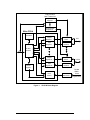
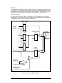
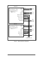
IP-UD-D
24 Line Differential
Input/Output
IndustryPack®
User Manual
© 1999, 2005 SBS Technologies, Inc.
Subject to change without notice.
Part # 89002074 Rev. 1.0
20050125
IP-UD-D
24 Line Differential Input/Output
IndustryPack®
SBS Technologies, Inc.
1284 Corporate Center Drive
St. Paul, MN 55121-1245
Tel (651) 905-4700
FAX (651) 905-4701
Email: [email protected]
http://www.sbs.com
© 1999, 2005 SBS Technologies, Inc.
IndustryPack and PC•MIP are a registered
trademarks of SBS Technologies, Inc. QuickPack,
SDpacK and Unilin are trademarks SBS
Technologies, Inc.
SBS Technologies, Inc acknowledges the
trademarks of other organizations for their respective
products mentioned in this document.
All rights are reserved: No one is permitted to
reproduce or duplicate, in any form, the whole or part
of this document without the express consent of SBS
Technologies. This document is meant solely for the
purpose in which it was delivered.
SBS Technologies reserves the right to make any
changes in the devices or device specifications
contained herein at any time and without notice.
Customers are advised to verify all information
contained in this document.
The electronic equipment described herein
generates, uses and may radiate radio frequency
energy, which can cause radio interference. SBS
Technologies assumes no liability for any damages
caused by such interference.
SBS Technologies’ products are not authorized for
use as critical components in medical applications
such as life support equipment, without the express
consent of the general manager of SBS
Technologies Commercial Group.
This product has been designed to operate with
IndustryPack, PC•MIP or CompactPCI modules or
carriers and compatible user-provided equipment.
Connection of incompatible hardware is likely to
cause serious damage. SBS Technologies assumes
no liability for any damages caused by such
incompatibility.
Table of Contents
Product Description.......................................................................................................................... 1
VMEbus Addressing ........................................................................................................................ 3
NuBus Addressing ........................................................................................................................... 7
ISA (IBM PC-AT) Addressing........................................................................................................... 8
I/O Pin Wiring ................................................................................................................................. 11
IndustryPack Logic Interface Pin Assignment ............................................................................... 12
Programming.................................................................................................................................. 13
ID PROM........................................................................................................................................ 15
Theory of Operation ....................................................................................................................... 16
Construction and Reliability ........................................................................................................... 21
Repair............................................................................................................................................. 22
Specifications ................................................................................................................................. 23
List of Figures
Figure 1
Figure 2
Figure 3
Figure 4
Figure 5
Figure 6
Figure 7
Figure 8
Figure 9
Figure 10
Figure 11
Figure 12
Figure 13
IP-UD-D Block Diagram.................................................................................... 2
Word Access VME Address Map ..................................................................... 3
Byte Access VME Address Map....................................................................... 4
Long Word Access VME Address Map ............................................................ 5
Word Access ISA Address Map ....................................................................... 8
Byte Access ISA Address Map......................................................................... 9
I/O Pin Assignment ......................................................................................... 11
Logic Interface Pin Assignment ...................................................................... 12
Control Register Bit Definitions....................................................................... 14
ID PROM Data (hex)..................................................................................... 15
I/O Line Block Diagram................................................................................. 17
Master and Slave Block Diagram ................................................................. 19
Master and Slave Configuration ................................................................... 20
Product Description
The IP-UD-D is part of the IndustryPackTM family of modular I/O components. It provides
24 lines of digital I/O, each with EIA-422 and EIA-485 (formerly RS422 and RS485)
compatible differential drivers and receivers. Each line may be dynamically and
individually configured for either input or output. Outputs may be double buffered,
making it possible to synchronize multiple IPs. Both internal read back and direct read
registers are provided for ease of software development. 16-bit word and 8-bit byte
operations are supported.
The IP-UD-D conforms to the IndustryPack Interface Specification. This guarantees
compatibility with multiple Support Modules. Because the IPs may be mounted on
different form factors while maintaining plug and software compatibility, system
prototyping may be done on one Support Module with final system implementation on a
different one.
The differential receiver for each line is always enabled, allowing the state of each I/O
line to be determined at any time. The output enable for each differential transmitter is
controlled by a bit in the Output Enable Register. Writing a zero to any bit in this register
enables the corresponding output driver. Writing a one to any bit disables the output
driver, allowing the I/O line to be used as an input. The power up default disables all the
output drivers.
Input and output lines may be double buffered by setting a bit in the Control Register.
When this bit is set, the user must provide an external clock of up to 1 MHz. Unlike the
other inputs, this is a single ended TTL level input. Another bit in the Control Register
selects the polarity of this clock, allowing inputs and outputs to be latched on either the
rising or falling clock edge. Any TTL compatible clock source may be used.
Two separate locations in I/O space are provided for each signal line. The first location is
used to set the output state and also to read back the written value at the internal latch.
This read back function is valuable to support bit operations (which are implemented by
processors as read-modify-write cycles). It is also useful in debugging, making it
possible to observe directly the last value written to the port. The second location is the
direct read port, which is always used for reading input values. This register may also be
used to verify the correct logic signal is actually on the interface cable.
The IP can function in a Master/Slave Mode for synchronizing multiple IPs. In this mode,
the Master IP re-drives the external clock source out I/O line 23. This line becomes the
Master Clock that should be wired to I/O line 24 on the Master and all Slave IPs. Wiring
in this way prevents excessive loading of the external clock source while ensuring all I/O
latches are clocked with minimal skew.
Figure 1 shows a block diagram of the IP-UD-D.
1
Output Control
Latch Transceiver
Output Enable
Register 1
Output Enable
Register 24
Xilinx FPGA
ID PROM
Output
Register 1
Differential
Driver
Input
Register 1
Differential
Receiver
Output
Register 24
Differential
Driver
Input
Register 24
Differential
Receiver
I/O 1
I/P Bus
Interface
Control
Register
Clock
Control
Figure 1
IP-UD-D Block Diagram
2
LineSafe
Esd Circuit
I/O 24
Double
Buffer
Clock
(Single Ended)
VMEbus Addressing
IP-UD-D normally is accessed one word at a time in the host's I/O space. Alternatively,
byte or long word accesses may be used. If long words are used, the host (or support
module) must map 32-bit long words into two 16-bit cycles. This is common for 68020
and 68030 implementation of the I/O space.
Standard Word Access, I/O Space
base + $0
base + $2
word
word
write
write
Output Lines 1—16
Output Lines 17—24
base + $0
base + $2
word
word
read
read
Read Back Lines 1—16
Read Back Lines 17—24
base + $4
base + $6
word
word
read
read
Direct Read Lines 1—16
Direct Read Lines 17—24
base + $8
base + $A
word
word
read/write Output Enable Lines 1—16
read/write Output Enable Lines 17—24
base + $C
word
read/write Control Register
Figure 2
Word Access VME Address Map
Bit map of words at base + $0 and base + $4
Data Bit #
I/O Line:
15
16
14
15
13
14
12
13
11
12
10
11
9
10
8
9
7
8
6
7
5
6
4
5
3
4
2
3
1
2
0
1
8
-
7
24
6
23
5
22
4
21
3
20
2
19
1
18
0
17
Bit map of words at base + $2 and base + $6
Data Bit #
I/O Line:
15
-
14
-
13
-
12
-
11
-
10
-
9
-
Note: data in bits 15 through 8 are ignored in writes, read as "0"s.
Bit map of words at base + $8
Data Bit #
Output En:
15
16
14
15
13
14
12
13
11
12
10
11
9
10
8
9
7
8
6
7
5
6
4
5
3
4
2
3
1
2
0
1
11
-
10
-
9
-
8
-
7
24
6
23
5
22
4
21
3
20
2
19
1
18
0
17
Bit map of words at base + $A
Data Bit #
Output En:
15
-
14
-
13
-
12
-
Note: data in bits 15 through 8 are ignored in writes, read as "0"s.
3
Bit map of word at base + $C
Data Bit #
Write:
Read:
[15:4]
0
3
Master Select
Master Select
2
Mode Enable
Mode Enable
1
Clock Polarity
Clock Polarity
Alternate Byte Access, I/O Space
base + $0
base + $1
base + $3
byte
byte
byte
write
write
write
Output lines 9—16
Output lines 1—8
Output lines 17—24
base + $0
base + $1
base + $3
byte
byte
byte
read
read
read
Read back lines 9—16
Read back lines 1—8
Read back lines 17—24
base + $4
base + $5
base + $7
byte
byte
byte
read
read
read
Direct read lines 9—16
Direct read lines 1—8
Direct read lines 17—24
base + $8
base + $9
base + $B
byte
byte
byte
read/write Output Enable Lines 9—16
read/write Output Enable Lines 1—8
read/write Output Enable Lines 17—24
base + $D
byte
read/write Control register
Figure 3
Byte Access VME Address Map
Bit map of bytes at base + $0 and base + $4
Data Bit #
I/O Line:
7
16
6
15
5
14
4
13
3
12
2
11
1
10
0
9
1
2
0
1
1
18
0
17
Bit map of bytes at base + $1 and base + $5
Data Bit #
I/O Line:
7
8
6
7
5
6
4
5
3
4
2
3
Bit map of bytes at base + $3 and base + $7
Data Bit #
I/O Line:
7
24
6
23
5
22
4
21
3
20
2
19
Bit map of bytes at base + $8
Data Bit #
Output En:
7
16
6
15
5
14
4
13
3
12
2
11
1
10
4
0
9
0
Dbl. Buffer En.
Dbl. Buffer En.
Bit map of bytes at base + $9
Data Bit #
Output En:
7
8
6
7
5
6
4
5
3
4
2
3
1
2
0
1
4
21
3
20
2
19
1
18
0
17
Bit map of bytes at base + $A
Data Bit #
Output En:
7
24
6
23
5
22
Bit map of byte at base + $D
Data Bit #
Write:
Read:
[7:4]
0
3
Master Select
Master Select
2
Mode Enable
Mode Enable
1
Clock Polarity
Clock Polarity
0
Dbl. Buffer En.
Dbl. Buffer En.
Alternate Long Word Access, I/O Space
base + $0
long
write
Output Lines 1—24
base + $0
long
read
Read Back Lines 1—24
base + $4
long
read
Direct Read Lines 1—24
base + $8
long
read/write Output Enable Lines 1—24
base + $C
long
read/write Control register
Figure 4
Long Word Access VME Address Map
Bit map of long words at base + $0 and base + $4
Data Bit #
I/O Line:
31
16
30
15
29
14
28
13
27
12
26
11
25
10
24
9
23
8
22
7
21
6
20
5
19
4
18
3
17
2
16
1
Data Bit #
I/O Line:
15
-
14
-
13
-
12
-
11
-
10
-
9
-
8
-
7
24
6
23
5
22
4
21
3
20
2
19
1
18
0
17
Note: data in bits 15 through 8 are ignored in writes, read as "0"s.
Bit map of long words at base + $8
Data Bit #
Output En:
31
16
30
15
29
14
28
13
27
12
26
11
25
10
24
9
23
8
22
7
21
6
20
5
19
4
18
3
17
2
16
1
Data Bit #
Output En:
15
-
14
-
13
-
12
-
11
-
10
-
9
-
8
-
7
24
6
23
5
22
4
21
3
20
2
19
1
18
0
17
Note: data in bits 15 through 8 are ignored in writes, read as "0"s.
5
Bit map of long word at base + $C
Data Bit #
Write:
Read:
[31:20]
0
19
Master Select
Master Select
18
Mode Enable
Mode Enable
17
Clock Polarity
Clock Polarity
16
Dbl. Buffer En.
Dbl. Buffer En.
Note: data in bits 31 through 20 and 15 through 0 are ignored in writes, read as "0"s.
6
[15:0]
0
NuBus Addressing
NuBus addressing requires computing the address from the byte addresses given above
under VMEbus Addressing. The formula is:
NuBus byte address = (VMEbus byte address * 2) – 1
All byte data is still transferred on data lines D7..D0.
Word addresses on the NuBus are the same as for VME. Word data is transferred on
data lines D15..D0.
7
ISA (IBM PC-AT) Addressing
IP-UD-D normally is accessed one word at a time in the host's I/O space. Alternatively,
byte accesses may be used. The actual application will depend on the carrier board.
See the carrier board manual for details.
Standard Word Access, I/O Space
base + $0
base + $2
word
word
write
write
Output Lines 1—16
Output Lines 17—24
base + $0
base + $2
word
word
read
read
Read Back Lines 1—16
Read Back Lines 17—24
base + $4
base + $6
word
word
read
read
Direct Read Lines 1—16
Direct Read Lines 17—24
base + $8
base + $A
word
word
read/write Output Enable Lines 1—16
read/write Output Enable Lines 17—24
base + $C
word
read/write Control register
Figure 5
Word Access ISA Address Map
Bit map of words at base + 0 and base + 4
Data Bit #
I/O Line:
15
16
14
15
13
14
12
13
11
12
10
11
9
10
8
9
7
8
6
7
5
6
4
5
3
4
2
3
1
2
0
1
9
-
8
-
7
24
6
23
5
22
4
21
3
20
2
19
1
18
0
17
Bit map of words at base + 2 and base + 6
Data Bit #
I/O Line:
15
-
14
-
13
-
12
-
11
-
10
-
Note: data in bits 15 through 8 are ignored in writes, read as "0"s.
Bit map of word at base + $C
Data Bit #
Write:
Read:
[15:4]
0
3
Master Select
Master Select
2
Mode Enable
Mode Enable
1
Clock Polarity
Clock Polarity
0
Dbl. Buffer En.
Dbl. Buffer En.
Bit map of words at base + $8
Data Bit #
Output En:
15
16
14
15
13
14
12
13
11
12
10
11
9
10
8
8
9
7
8
6
7
5
6
4
5
3
4
2
3
1
2
0
1
Bit map of words at base + $A
Data Bit #
Output En:
15
-
14
-
13
-
12
-
11
-
10
-
9
-
8
-
7
24
6
23
5
22
4
21
3
20
2
19
1
18
0
17
Note: data in bits 15 through 8 are ignored in writes, read as "0"s.
Bit map of word at base + $C
Data Bit #
Write:
Read:
[15:4]
0
3
Master Select
Master Select
2
Mode Enable
Mode Enable
1
Clock Polarity
Clock Polarity
Alternative Byte Access, I/O Space
base + $0
base + $1
base + $2
byte
byte
byte
write
write
write
Output Lines 1 through 8
Output Lines 9 through 16
Output Lines 17 through 24
base + $0
base + $1
base + $2
byte
byte
byte
read
read
read
Read-back Lines 1 through 8
Read-back Lines 9 through 16
Read-back Lines 17 through 24
base + $4
base + $5
base + $6
byte
byte
byte
read
read
read
Direct Read Lines 1 through 8
Direct Read Lines 9 through 16
Direct Read Lines 17 through 24
base + $8
base + $9
base + $A
byte
byte
byte
read/write Output Enable Lines 1—8
read/write Output Enable Lines 9—16
read/write Output Enable Lines 17—24
base + $C
byte
read
Figure 6
Control Register
Byte Access ISA Address Map
Bit map of bytes at base + $0 and base + $4
Data Bit #
I/O Line:
7
8
6
7
5
6
4
5
3
4
2
3
1
2
0
1
Bit map of bytes at base + $1 and base + $5
Data Bit #
I/O Line:
7
16
6
15
5
14
4
13
3
12
2
11
1
10
0
9
1
18
0
17
Bit map of bytes at base + $2 and base + $6
Data Bit #
I/O Line:
7
24
6
23
5
22
4
21
3
20
2
19
9
0
Dbl. Buffer En.
Dbl. Buffer En.
Bit map of bytes at base + $8
Data Bit #
Output En:
7
8
6
7
5
6
4
5
3
4
2
3
1
2
0
1
4
13
3
12
2
11
1
10
0
9
4
21
3
20
2
19
1
18
0
17
Bit map of bytes at base + $9
Data Bit #
Output En:
7
16
6
15
5
14
Bit map of bytes at base + $A
Data Bit #
Output En:
7
24
6
23
5
22
Bit map of byte at base + $C
Data Bit #
Write:
Read:
[7:4]
0
3
Master Select
Master Select
2
Mode Enable
Mode Enable
10
1
Clock Polarity
Clock Polarity
0
Dbl. Buffer En.
Dbl. Buffer En.
I/O Pin Wiring
This section gives the pin assignments and wiring recommendations for IP-UD-D.
The pin numbers given in Figure 7 below correspond to numbers on the 50-pin
IndustryPack I/O connector, to the wires on a 50-pin flat cable plugged into a standard IP
carrier board, and to the screw terminal numbers on the IP-Terminal block.
I/O 1+
I/O 2+
I/O 3+
I/O 4+
I/O 5+
I/O 6+
I/O 7+
I/O 8+
I/O 9+
I/O 10+
I/O 11+
I/O 12+
I/O 13+
I/O 14+
I/O 15+
I/O 16+
I/O 17+
I/O 18+
I/O 19+
I/O 20+
I/O 21+
I/O 22+
I/O 23+/Master Clk Out+
I/O 24+/Slave Clk In+
Double Buffer Clk
1
3
5
7
9
11
13
15
17
19
21
23
25
27
29
31
33
35
37
39
41
43
45
47
49
Figure 7
I/O 1–
I/O 2–
I/O 3–
I/O 4–
I/O 5–
I/O 6–
I/O 7–
I/O 8–
I/O 9–
I/O 10–
I/O 11–
I/O 12–
I/O 13–
I/O 14–
I/O 15–
I/O 16–
I/O 17–
I/O 18–
I/O 19–
I/O 20–
I/O 21–
I/O 22–
I/O 23–/Master Clk Out–
I/O 24–/Slave Clk In–
GND
I/O Pin Assignment
11
2
4
6
8
10
12
14
16
18
20
22
24
26
28
30
32
34
36
38
40
42
44
46
48
50
IndustryPack Logic Interface Pin
Assignment
Figure 8 below gives the pin assignments for the IndustryPack Logic Interface on the
IP-UD-D. Pins marked n/c below are defined by the specification, but are not used on IPUD-D. Also see the User Manual for your IP Carrier board for more information.
GND
CLK
Reset*
D0 IDSel*
D1 n/c
D2 n/c
D3 n/c
D4 INTSel*
D5 n/c
D6 IOSel*
D7 n/c
D8 A1
D9 n/c
D10
D11
D12
D13
D14
D15
BS0*
BS1*
–12V
+12V
+5V
GND
GND
+5V
R/W*
4
5
6
7
8
9
10
11
12
13
A2
n/c
A3
n/c
A4
n/c
A5
n/c
A6
Ack*
n/c
GND
1
26
2
3
27
28
29
30
31
32
33
34
35
36
37
38
14
15
16
17
18
19
20
21
22
23
39
40
41
42
43
44
45
46
47
48
24
25
49
50
Note 1: The no-connect (n/c) signals above are defined by the IndustryPack Logic Interface
Specification, but not used by this IP. See the Specification for more information.
Note 2: The layout of the pin numbers in this table corresponds to the physical placement
of pins on the IP connector. Thus this table may be used to easily locate the physical pin
corresponding to a desired signal. Pin 1 is marked with a square pad on the IndustryPack.
Figure 8
Logic Interface Pin Assignment
12
Programming
Programming the IP requires only the ability to read and write data in the host's I/O
space. The base address is determined by the IP Support Module. This document
refers to this address as "base".
After power on reset or VME system reset, the IP requires a minimum delay of 300
milliseconds before any accesses are made by the host system. This is to allow the
Xilinx FPGA to configured itself. Any accesses during this time will result in a bus error.
Reset sets all lines to be inputs and clears all bits in the Control Register.
Each of the 24 I/O lines has a differential transceiver on it. This makes it possible to
individually set each bit as input or output. The receiver circuit in the transceiver is
always enabled, allowing the user to read the state of the I/O line at any time. The
transmitter circuit in the transceiver must be enabled to make a bit an output. The enable
for each transmitter is controlled by a corresponding bit in the Output Control Register.
Writing a "0" to a bit in the Output Control Register will turn on that bit's output
transmitter, making it an output. The value written to the Output Register will then appear
on the I/O line. Writing a "1" to a bit in the Output Control Register will turn off the
transmitter, making the bit an input. The Output Control Register defaults to all "1"s on
reset, disabling all the output transmitters.
Data may be read from two sets of address locations. The first set of locations, base +
0x0 and base + 0x2 for word operations, function as the Internal Read Back Register.
The data latched in the Output Latch is read from these addresses. They support
processor bit operations implemented as read-modify-write cycles, and are also useful
for debugging purposes.
The second set of locations, base + 0x4 and base + 0x6 for word operations, is the Direct
Read Register. Data is latched into the Input Register on the rising edge of the 8 MHz IP
Clock. Figure 10 in the Theory of Operations section shows a block diagram.
Using word access, up to 16 bits may be programmed at once. The IP implements a read
back register at the same address used for writing to the signal line I/O bits. This permits
"set bit" and "clear bit" instructions to be used in programming, which are implemented by
the host hardware as read-modify-write cycles. Thus, single bits at well as bit fields may
be accessed.
The IP may also be accessed using byte or long word accesses. If long word accesses
are used from a 68020, 68030, or 68040 host, the I/O space must be mapped into "D16".
68000 and 68010 hosts internally map all long word accesses into 16 bits, so no special
precaution is necessary.
The IP uses a Control Register to enable double buffering and control the polarity of the
Double Buffer Clock. It also is used to enable Master/Slave Mode and define the Master
IP in a multiple IP system using an external clock source to synchronize inputs and
outputs.
13
Bit #
0
1
2
3
4—7
Definition
Double Buffer Enable
Double Buffer Clock Polarity
Select
Mode Enable
Master Select
Reserved
Figure 9
Access
Read/Write
Read/Write
Read/Write
Read/Write
Read as "0"
Control Register Bit Definitions
Control Register Bit Definitions:
Bit [0] = D0 LSB
Double Buffer Enable
This bit enables double buffering. If this bit is set to a "1", the user must provide either a
single ended TTL level clock on the Double Buffer Clock, pin 49, or a differential clock on
the Slave Clock, pins 45 and 46, depending on how bit[3] is set. This clock may be up to
1 MHz. A clock source with an edge rate faster than 60 ns. must be used for the Double
Buffer Clock. Writing a "0" disables double buffering. This is the default.
Bit [1] = D1
Double Buffer Clock Polarity Select
This bit controls the Double Buffer Clock polarity. Writing a "1" will cause output data to
be latched out of the IP and input data to be latched into the IP on the falling edge of the
Double Buffer Clock. Writing a "0" will cause data to be latched on the rising edge of the
Double Buffer Clock. This is the default.
Bit [2] = D2
Master/Slave Mode Enable
This bit determines which pin on the I/O connector is the source for the Double Buffer
Clock. Writing a "1" puts the IP in Master/Slave mode and makes pins 47 and 48 (I/O 24)
the source for the Double Buffer Clock. In this mode, O24 En in the Output Control
Register must be set to "1" to make I/O line 24 an input. This I/O line must be set up
prior to putting the IP in Master Mode. Writing a "0" to the Master/Slave Mode Enable
bit puts the IP in normal mode and makes pin 49 (Double Buffer Clock) the source for the
Double Buffer Clock. In this mode, all 24 I/O lines are available for use. This is the
default mode.
Bit [3] = D3
Master Select
This bit determines whether the IP is a master or slave. Writing a "1" makes the IP a
master. When it is a master, the IP re-drives the Double Buffer Clock (pin 49) out I/O line
23 (pins 45 and 46). This clock should then be wired externally to I/O line 24 (pins 47
and 48) on this IP and all slave IPs. This minimizes the clock skew between the master
and all slaves. When this bit is set, O23 En in the Output Control Register must be set to
"0" to make I/O line 23 an output and O24 En must be set to a "1" to make I/O line 24 an
input. These I/O lines must be set up prior to putting the IP in Master Mode. Writing
a "0" to the Master Select bit makes the IP a slave with its clock source I/O line 24 if Bit
[2] is set to a "1", or normal operation with its Double Buffer Clock source from pin 49
(Double Buffer Clock). This is the default. See Figure 12 in the Theory of Operation
section later in this manual for a diagram of how to wire a master and slave IP.
Bit [7..4] = D7..D4
Reserved
These bits are reserved for future use and will be read as "0".
14
ID PROM
Every IP contains an IP PROM, whose size is at least 32 x 8 bits. The ID PROM aids in
software auto configuration and configuration management. The user’s software, or a
supplied driver, may verify that the device it expects is actually installed at the location it
expects and is nominally functional. The ID PROM contains the manufacturing revision
level of the IP. If a driver requires a particular revision IP, it may check for it directly.
Standard data in the ID PROM on the IP-UD-D is shown in Figure 10 below. For more
information on IP ID PROMs refer to the IndustryPack Logic Interface Specification,
available from SBS Technologies. The ID PROM on the IP-UD-D is implemented in the
Xilinx FPGA device.
The location of the ID PROM in the host’s address space is dependent on the carrier
board used. For most VMEbus carriers the ID PROM space is directly above the IP’s I/O
space, or at IP-base + $80. Macintosh drivers use the ID PROM automatically. RM1260
address may be derived from Figure 10 below by multiplying the addresses given by two,
then subtracting one. RM1270 addresses may be derived by multiplying the addresses
given by two, then adding one.
3F
(available for user)
19
17
15
13
11
0F
0D
0B
09
07
05
03
01
CRC for bytes used
No of bytes used
Driver ID, high byte
Driver ID, low byte
reserved
Revision
Model No IP-UD-D
Manufacturer ID SBS (GreenSpring)
ASCII “C”
ASCII “A”
ASCII “P”
ASCII “I”
Figure 10
ID PROM Data (hex)
15
(20)
(0C)
(00)
(00)
(00)
(A1)
(62)
(F0)
(43)
(41)
(50)
(49)
Theory of Operation
IndustryPack Standards
The IP-UD-D is part of the IndustryPackTM family of modular I/O products. It meets the
IndustryPack Logic Specification. (Contact SBS Technologies. for a copy of this
Specification.) It is assumed the reader is at least casually familiar with both this
document and 68000 processor architecture.
Control Logic
All control logic is contained within a single Xilinx FPGA. It is clocked by the 8 MHz IP
Logic clock from the Support Module. The IP responds to I/O and ID selects. It does not
respond to memory selects, however the MEMSel* line is routed to the FPGA, enabling
easy modification for special needs.
The IP does not require wait states for either read or write cycles. Thus, the FPGA
generates Ack* on the clock cycle following either I/O or ID Select. Hold cycles (from the
Support Module) are supported for both read and write cycles by extending Ack* as
required. If no hold cycles are requested by the Support Module, the IP is capable of
supporting the full 8 MByte per second data transfer rate of the IP Logic Interface
Specification.
I/O Data Lines
All input and output latches are contained within the Xilinx FPGA. Each I/O line has a
EIA-485/EIA-422 differential transceiver with an extended common mode range of +12V
to -7V. A socketed 8 pin SIP resistor network provides parallel termination to groups of
four transceivers. A 100Ω value is the factory default value, though the user may
substitute other values to match the characteristic impedance of the I/O cables. The
resistor network may be removed if no termination is desired, or individual leads may be
cut off if terminations are required only for specific I/O lines.
Data Output
Each differential transceiver's transmitter has an output enable that is controlled by a
corresponding bit in the Output Enable Register. When the bit in the Output Enable
Register is set to a "0", the transmitter is enabled and the data written to the Output
Register will appear on the I/O line. When the bit in the Output Enable Register is set to
a "1", the transmitter outputs maintain a high impedance over the entire common mode
range.
Each output has two latches associated with it. If double buffering is enabled, the Double
Buffer Latch is clocked by the Double Buffer Clock. Without double buffering, this latch is
clocked on the falling edge of the IP Clock. Figure 11 shows a block diagram. Outputs
from the Double Buffer Latch drive the differential transmitters. Data is latched into the
internal latch on the rising edge of the IP Clock after the IOSel* line is driven low.
Double buffering is enabled by setting the Double Buffer Enable Bit (bit [0]) in the Control
Register to a "1". A single ended TTL compatible signal must be provided on the
External Clock, pin 49. This signal must have an edge rate faster than 60 ns. If double
buffering is enabled, the Double Buffer Clock Polarity Bit (bit [1]) in the Control Register is
used to set the Double Buffer Clock polarity. Setting the Double Buffer Clock Polarity Bit
to a "0" will latch data on the rising edge and setting it to a "1" will latch data on the falling
edge. The power up default is "0" for both these bits.
16
Data Input
The data may be read from two sets of address locations. The first set of locations, base
+ 0 and base + 2 for word operations, function as the Internal Read Back Register. The
data latched in the Internal Latch is read from these addresses. They support processor
bit operations implemented as read-modify-write cycles, and are also useful for
debugging purposes.
The second set of locations, base + 4 and base + 6 for word operations, is the Direct
Read Register. Data is latched into Input Register with the same clock which latches the
Double Buffer Latch. Figure 11 shows a block diagram.
Output Enable
Register
8 MHz
IP Clk
D Q
Internal
Latch
Double Buffer
Latch
D Q
D Q
I/O Line +
100ž
I/O Line –
Read Back
Buffer
Y A
Input
Latch
Data Bus
Q D
Double
Buffer Clk
Clk Pol. Sel.
Double Buffer
Enable
Figure 11
I/O Line Block Diagram
17
Master/Slave Mode
Master/Slave Mode is provided for multiple IP systems using a single external clock to
synchronize inputs and outputs. If this clock does not have sufficient drive capability for
driving all the IPs in the system, it may be wired to the Master IP to be re-driven to all the
Slave IPs. Figure 12 shows a block diagram of two IPs in Master/Slave Mode while
Figure 13 shows a diagram of how to wire a Master and Slave IP.
An IP is configured to be a Master by setting both the Master/Slave Mode Bit and the
Master Select Bit (bit [2] and bit [3]) to a "1" in the Control Register. The desired clock
polarity is set by the Clock Polarity Select Bit (bit [1]). Writing a "0" to this bit will latch
data on the rising edge, writing a "1" will latch data on the falling edge. I/O Line 24 is set
to be an output by writing a "0" to OEn 24 in the Output Control Register, while I/O Line
23 is set to be an input by writing a "1" to OEn 23. The Output Enables for the I/O lines
must be set up before the Master/Slave Mode is enabled. The external clock is wired to
the Double Buffer Clk pin 49. The Master Clk Out pins 45 and 46 are then wired to the
Slave Clk In, pins 47 and 48 on all the IPs, including the Master IP.
Slave IPs are configured by setting the Master/Slave Mode Bit (bit [2]) to a "1" and the
Master Select Bit (bit [3]) to a "0" in the Control Register. The desired clock polarity is set
by the Clock Polarity Select Bit (bit [1]). I/O Line 24 is set to be an input by writing a "1"
to OEn24 in the Output Control Register. The Master Clk Out signal from the Master IP
is wired to the Slave Clk In, pins 47 and 48.
The termination resistors should be removed for the Master Clk Out signal and all Slave
Clk In signals except for the receiver farthest from the Master. This is shown in Figure
12. A termination resistor is removed by cutting one of the leads on the resistor network.
Before removing a resistor network, note which direction pin 1 is facing (pin 1 has a small
dot marked on the resistor network body above the pin). To remove a termination
resistor, remove the resistor network, and cut off the lead on the pin corresponding to the
I/O line, then replace the resistor network. The Master IP should have pins 2 and 4 of
RN3 cut, while all Slave IPs except the one farthest from the Master should have pin 1 of
RN3 cut.
18
Master IP
I/O 1+
I/O 1–
Double
Buffer
I/O 22+
I/O 22+
Master Clk Out+
Master Clk Out–
Slave Clk In+
Slave Clk In–
External Clk In
Termination Resistors removed
To other Slave IPs
Slave IP
I/O 1+
I/O 1–
Double
Buffer
I/O 23+
I/O 23–
Slave Clk In+
Slave Clk In–
Only on last Slave IP
Figure 12
Master and Slave Block Diagram
19
Master IP
Control Register = 0B\h
Output Control Register:
OEn 24 = "1"
OEn 23 = "0"
I/O 1 +
I/O 1 –
I/O 22 +
I/O 22 –
Master Clk Out +
Master Clk Out –
Slave Clk In +
Slave Clk In –
External Clk
Slave IP
Control Register = 05\h
Output Control Register:
OEn 24 = "1"
I/O 1 +
I/O 1 –
I/O 23 +
I/O 23 –
Slave Clk In +
Slave Clk In –
External Clk
Pin 1
Pin 2
Pin 43
Pin 44
Pin 45
I/O –
Pin 47
Pin 48
Pin 49
Pin 1
Pin 2
Pin 45
Pin 46
Pin 47
TTL
Level
Clock
I/O +
I/O –
I/O +
I/O –
Pin 48
Pin 49
Master and Slave Configuration
20
I/O +
Pin 46
To other Slave IPs
Figure 13
I/O +
I/O –
n/c
Construction and Reliability
IndustryPacks were conceived and engineered for rugged industrial environments. The
IP-UD-D is constructed out of 0.062 inch thick FR4 V0 material. The six copper layers
consist of two signal layers on the top and bottom, and four internal layers. Two internal
layers are dedicated to power and ground planes and two are used for signal wiring.
Through hole and surface mounting of components are used. IC sockets use gold plated
screw-machine pins. High insertion and removal forces are required, which assists in
keeping components in place. If the application requires unusually high reliability or is in
an environment subject to high vibration, the user may solder the four corner pins of each
socketed IC into the socket, using a grounded soldering iron.
The IndustryPack connectors are keyed, shrouded and have gold plated pins on both
plugs and receptacles. They are rated at 1 Amp per pin, 200 insertion cycles minimum.
These connectors make consistent, correct insertion easy and reliable.
The IP is secured to the carrier with four M2 metric stainless steel screws. The heads of
the screws are countersunk into the IP. The four screws provide significant protection
against shock, vibration and incomplete insertion. For most applications they are not
required.
The IndustryPack provides a low temperature coefficient of 0.89 W/°C for uniform heat.
This is based on the temperature coefficient of the base FR4 material of 0.31 W/m-°C,
taking into account the thickness and area of the IP. This coefficient means that if 0.89
Watts is applied uniformly on the component side, then the temperature difference
between the component and the solder side is one degree Celsius.
21
Repair
Service Policy
Before returning a product for repair, verify as soon as possible that the suspected unit is
at fault; then call the Customer Service Department for a RETURN MATERIAL
AUTHORIZATION (RMA) number. Carefully package the unit, in the original shipping
carton if it is available, and ship prepaid and insured with the RMA number clearly written
on the outside of the package. Include the return address and telephone number of a
technical contact. For out-of-warranty repairs, a purchase order for repair charges must
accompany the return. SBS Technologies will not be responsible for damages due to
improper packaging of returned items. For service of SBS Technologies products not
purchased directly from SBS Technologies, contact your reseller. Products returned to
SBS Technologies for repair by other than the original customer will be treated as out-ofwarranty.
For service, contact:
SBS Technologies, Inc.
1284 Corporate Center Drive
St. Paul, MN 55121-1245
Tel: (651) 905-4700
FAX: (651) 905-4701
Email: [email protected]
22
Specifications
Size
Single High Industry Pack.
Digital Interface
24 digital signal lines with double buffered inputs and
outputs.
Each line is either an input or an output.
Interface Level
EIA-485/EIA-422 Differential Interface.
Common Mode Voltage Range +12V/–7V.
Software Interface
The 24 I/O lines are read or written with either word or
byte accesses.
There is an 8-bit Control Register.
Initialization
300 Millisecond delay from reset.
Forces all lines to be inputs.
Disables double buffering.
Access Mode
Byte or word in I/O Space.
Wait States
Zero.
Transfer Rate
8 Mbytes/second maximum, continuous.
Onboard Options
All options are software programmable.
Dimensions
Standard Single High IndustryPack width and length
1.8 x 3.9 inches.
Construction
Conformal Coated FR4 4 layer Printed Circuit.
Surface mounted components.
Temperature Coefficient
0.89 W/°C for uniform heat across IP.
Power Requirements
+5.0 VDC, 60 mA typical.
23