1
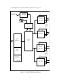
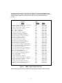
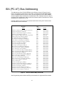
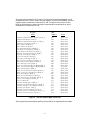
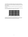
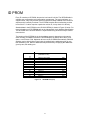
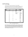
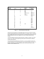
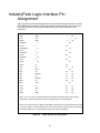
IP-UNIV-SERIAL
Dual Channel
High Speed Serial
IndustryPack
User Manual
© 1999-2005 SBS Technologies, Inc.
Subject to change without notice.
Part # 89002082 Rev. 1.0
20050127
IP-UNIV-SERIAL
Dual Channel
High Speed Serial
IndustryPack
SBS Technologies, Inc.
1284 Corporate Center Drive
St. Paul, MN 55121-1245
Tel (651) 905-4700
FAX (651) 905-4701
Email: [email protected]
http://www.sbs.com
©1999-2005 SBS Technologies, Inc.
IndustryPack and PC•MIP are a registered
trademarks of SBS Technologies, Inc. QuickPack,
SDpacK and Unilin are trademarks SBS
Technologies, Inc.
SBS Technologies, Inc acknowledges the
trademarks of other organizations for their
respective products mentioned in this document.
All rights are reserved: No one is permitted to
reproduce or duplicate, in any form, the whole or
part of this document without the express consent of
SBS Technologies. This document is meant solely
for the purpose in which it was delivered.
SBS Technologies reserves the right to make any
changes in the devices or device specifications
contained herein at any time and without notice.
Customers are advised to verify all information
contained in this document.
The electronic equipment described herein
generates, uses and may radiate radio frequency
energy, which can cause radio interference. SBS
Technologies assumes no liability for any damages
caused by such interference.
SBS Technologies’ products are not authorized for
use as critical components in medical applications
such as life support equipment, without the express
consent of the president of SBS Technologies.
This product has been designed to operate with
IndustryPack, PC•MIP or CompactPCI modules or
carriers and compatible user-provided equipment.
Connection of incompatible hardware is likely to
cause serious damage. SBS Technologies assumes
no liability for any damages caused by such
incompatibility.
Table of Contents
Product Description............................................................................................................. 5
VMEbus Addressing ........................................................................................................... 7
NuBus Addressing .............................................................................................................. 9
ISA (PC-AT) Bus Addressing............................................................................................ 10
Programming..................................................................................................................... 12
ID PROM........................................................................................................................... 17
I/O Pin Wiring .................................................................................................................... 18
IndustryPack Logic Interface Pin Assignment .................................................................. 20
Construction and Reliability .............................................................................................. 21
Repair................................................................................................................................ 22
Specifications IP-UNIV-SERIAL........................................................................................ 23
3
List of Figures
Figure 1
IP-UNIV-SERIAL Resistor Pack Configuration................................................. 5
Figure 2
IP-UNIV-SERIAL Block Diagram ...................................................................... 6
Figure 3
VMEbus Address Map (Channel B).................................................................. 7
Figure 4
VMEbus Address Map (Channel A).................................................................. 8
Figure 5
ISA bus Address Map (Channel B)................................................................. 10
Figure 6
ISA bus Address Map (Channel A)................................................................. 11
Figure 7
IndustryPack Control Register........................................................................ 12
Figure 8
Channel A Receiver Controls ......................................................................... 13
Figure 9
Channel B Receiver Controls ......................................................................... 13
Figure 10
External Clock Interface Controls ................................................................. 14
Figure 11
Valid IPCR Configurations............................................................................ 14
Figure 12
Transmission Line Driver Controls ............................................................... 15
Figure 13
Modem Controls ........................................................................................... 15
Figure 14
IndustryPack Control Register Values for Testing........................................ 16
Figure 15
ID PROM Data (hex)..................................................................................... 17
Figure 16
I/O Pin Definitions (Channel A)..................................................................... 18
Figure 17
I/O Pin Definitions (Channel B)..................................................................... 19
Figure 18
Logic Interface Pin Assignment .................................................................... 20
4
Product Description
The IP-UNIV-SERIAL is part of the IndustryPack® family of modular I/O components. It is
an upgrade to the IP-Serial. The pin assignments and basic features remain essentially
the same but the address map and register formats have changed. IP-UNIV-SERIAL
provides internal data buffering, data rates up to 10 megabits per second, and support for
nearly all serial protocols. The IP-UNIV-SERIAL incorporates the Zilog Z16C30 Universal
Serial Controller (USC) which includes 32 byte FIFO buffers for both transmit and receive
data on each of the two independent channels. Protocols supported by the Z16C30
include HDLC, SDLC, Bisync, NRZ, NRZI, and Biphase. Additional capabilities include 16
and 32-bit CRC generation and checking, one to eight bits per character, one
address/data bit, MIL STD 1553B protocol support, sync stripping, preamble generation,
and digital phase-locked loop circuits for clock recovery. The USC provides a flexible bus
interface architecture that is configured by the first write to the device, refer to the Zilog
documentation for details on Z16C30 programming.
The IP-UNIV-SERIAL includes an on board 3.6864 MHz oscillator that can be prescaled
with the Z16C30 to create all of the standard baud rates. A separate socket is provided
for a user oscillator. A single external clock interface is provided so that the IP-UNIVSERIAL can either operate from an external reference clock or provide an external
reference clock.
Channel A and Channel B within the USC device are almost completely independent.
Each channel has a complete prescaler, vector register, interrupt controller, and protocol
controller. Both channels share the external clock interface. Refer to the Zilog
documentation for details on the Z16C30.
Independent interrupt vectors and controls are provided for each IP-UNIV-SERIAL
channel. Channel A is given priority over Channel B in the event of simultaneous interrupt
requests. If Channel B asserts an interrupt request before Channel A, then the Channel A
interrupt request will be held off until the Channel B interrupt is acknowledged. Interrupt
priority and sequencing is controlled by a programmable device. Please contact SBS if
your application has special requirements.
The RS-232, RS-422, and RS-485 compatible interface circuit facilitates interfacing with
a wide variety of equipment. Three SIP resistor packs are used to configure the electrical
characteristics of the serial I/O interface. RP3 is a pull-up package used to control the
current available to the “reference” pin of the receivers during single ended operation.
During RS-232 operation the ‘+’ side of the differential receivers is set to approximately 3
volts. The minus side is used as the RS-232 input. RP1 and RP2 are packaged discrete
resistors used as terminating resistors for differential operation. The standard IP is
supplied with a nominal resistance of 100Ω. The user may select and install alternate SIP
resistors to optimize the termination for the application. RP1 and RP2 should not be
installed for single ended configurations to prevent the drive voltage from being applied to
the reference pin. RP3 should not be installed during differential operation. However; in
most cases, the small current drain added by RP3 will not result in improper operation.
Serial
Interface
RS-232
RS-422
RS-485
Figure 1
Resistor Packs Installed
RP3 (2KΩ)
RP1 and RP2 (100Ω)
RP1 and RP2 (100Ω)
Resistor Packs
Removed
RP1 and RP2 (100Ω)
RP3 (2KΩ)
RP3 (2KΩ)
IP-UNIV-SERIAL Resistor Pack Configuration
5
A block diagram of the IP-UNIV-SERIAL is shown below in Figure 2.
RS-485
RS-422
External
Clock
B
A
TTL
->
RS-485
RS232
RS-422
3.6864 MHz.
Clo c k
se le ct
B
A
I/P
Bu s
In te rfa ce
Z16C30
USC
TXD
RTS
DTR
TTL
->
RS422
RS-232
B
A
RS422
->
RS-485
TTL
RS-422
ID
PROM
B
Co n tro l
Re g iste r
A
IPCR
Figure 2
RS232
->
TTL
RS-232
IP-UNIV-SERIAL Block Diagram
6
RXD
CTS
DSR
DCD
VMEbus Addressing
The address map of the IP-UNIV-SERIAL on the VMEbus is given in Figures 3 and 4
below. All registers are accessed in IP I/O space. The Receive/Transmit Data Register
can be accessed as either a word or a byte. All other registers on the IP-UNIV-SERIAL
are word registers. Byte accesses are on data lines D7..D0. Word access are on data
lines D15..D0.
Interrupt mapping is a function of the selected carrier board. See your IP carrier board
User Manual for more information.
Register
Name
68K
Address
Channel Command/Address Register (CCAR_B)
Channel Mode Register (CMR_B)
Channel Command/Status Register (CCSR_B)
Channel Control Register (CCR_B)
Bus Configuration Register [first write only] (BCR)
IndustryPack Control Register (IPCR)
Test Mode Data Register (TMDR_B)
Test Mode Control Register (TMCR_B)
Clock Mode Control Register (CMCR_B)
Hardware Configuration Register (HCR_B)
Interrupt Vector Register (IVR_B)
I/O Control Register (IOCR_B)
Interrupt Control Register (ICR_B)
Daisy-Chain Control Register (DCCR_B)
Misc. Interrupt Status Register (MISR_B)
Status Interrupt Control (SICR_B)
Receive/Transmit Data Register (RDR/TDR_B)
Receive/Transmit Data Register (RDR/TDR_B)
Receive Mode Register (RMR_B)
Receive Command/Status Register (RCSR_B)
Receive Interrupt Control Register (RICR_B)
Receive Sync Register (RSR_B)
Receive Count Limit Register (RCLR_B)
Receive Character Count Register (RCCR_B)
Time Constant 0 Register (TC0R_B)
Alias of address $20
Transmit Mode Register (TMR_B)
Transmit Command/Status Register (TCSR_B)
Transmit Interrupt Control Register (TICR_B)
Transmit Sync Register (TSR_B)
Transmit Count Limit Register (TCLR_B)
Transmit Character Count Register (TCCR_B)
Transmit Constant 1 Register (TC1R_B)
Figure 3
$00
$02
$04
$06
$08
$0A
$0C
$0E
$10
$12
$14
$16
$18
$1A
$1C
$1E
$20
$21
$22
$24
$26
$28
$2A
$2C
$2E
$30
$32
$34
$36
$38
$3A
$3C
$3E
Access
Word, R/W
Word, R/W
Word, R/W
Word, R/W
Word, W
Word, R/W
Word, R/W
Word, R/W
Word, R/W
Word, R/W
Word, R/W
Word, R/W
Word, R/W
Word, R/W
Word, R/W
Word, R/W
Word, R/W
Byte, R/W
Word, R/W
Word, R/W
Word, R/W
Word, R/W
Word, R/W
Word, R/W
Word, R/W
Word, R/W
Word, R/W
Word, R/W
Word, R/W
Word, R/W
Word, R/W
Word, R/W
Word, R/W
VMEbus Address Map (Channel B)
See Programming section below and Zilog documentation for register definition details.
7
All registers are accessed in IP I/O space. The Receive/Transmit Data Register can be
accessed as either a word or a byte. All other registers on the IP-UNIV-SERIAL are word
registers. Byte accesses are on data lines D7..D0. Word access are on data lines
D15..D0.
Register
Name
Channel Command/Address Register (CCAR_A)
Channel Mode Register (CMR_A)
Channel Command/Status Register (CCSR_A)
Channel Control Register (CCR_A)
Spare Address, No Register
Spare Address, No Register
Test Mode Data Register (TMDR_A)
Test Mode Control Register (TMCR_A)
Clock Mode Control Register (CMCR_A)
Hardware Configuration Register (HCR_A)
Interrupt Vector Register (IVR_A)
I/O Control Register (IOCR_A)
Interrupt Control Register (ICR_A)
Daisy-Chain Control Register (DCCR_A)
Misc. Interrupt Status Register (MISR_A)
Status Interrupt Control (SICR_A)
Receive/Transmit Data Register (RDR/TDR_A)
Receive/Transmit Data Register (RDR/TDR_A)
Receive Mode Register (RMR_A)
Receive Command/Status Register (RCSR_A)
Receive Interrupt Control Register (RICR_A)
Receive Sync Register (RSR_A)
Receive Count Limit Register (RCLR_A)
Receive Character Count Register (RCCR_A)
Time Constant 0 Register (TC0R_A)
Alias of address $60
Transmit Mode Register (TMR_A)
Transmit Command/Status Register (TCSR_A)
Transmit Interrupt Control Register (TICR_A)
Transmit Sync Register (TSR_A)
Transmit Count Limit Register (TCLR_A)
Transmit Character Count Register (TCCR_A)
Transmit Constant 1 Register (TC1R_A)
Figure 4
68K
Address
Access
$40
$42
$44
$46
$48
$4A
$4C
$4E
$50
$52
$54
$56
$58
$5A
$5C
$5E
$60
$61
$62
$64
$66
$68
$6A
$6C
$6E
$70
$72
$74
$76
$78
$7A
$7C
$7E
Word, R/W
Word, R/W
Word, R/W
Word, R/W
Word, R/W
Word, R/W
Word, R/W
Word, R/W
Word, R/W
Word, R/W
Word, R/W
Word, R/W
Word, R/W
Word, R/W
Word, R/W
Word, R/W
Word, R/W
Byte, R/W
Word, R/W
Word, R/W
Word, R/W
Word, R/W
Word, R/W
Word, R/W
Word, R/W
Word, R/W
Word, R/W
Word, R/W
Word, R/W
Word, R/W
Word, R/W
Word, R/W
Word, R/W
VMEbus Address Map (Channel A)
See Programming section below and Zilog documentation for register definition details.
8
NuBus Addressing
NuBus addressing requires computing the address from the byte addresses given above
under VMEbus Addressing. The formula is:
NuBus byte address = (VMEbus byte address * 2) – 1
All byte data is still transferred on data lines D7..D0.
Word addresses on the NuBus are the same as for VME. Word data is transferred on
data lines D15..D0.
Interrupt mapping is a function of the selected carrier board. See your IP carrier board
User Manual for more information.
9
ISA (PC-AT) Bus Addressing
The address map of the IP-UNIV-SERIAL on the ISA bus is given in Figures 5 and 6
below. All registers are accessed in IP I/O space. The Receive/Transmit Data Register
can be accessed as either a word or a byte. All other registers on the IP-UNIV-SERIAL
are word registers. Byte accesses are on data lines D7..D0. This byte is the even byte in
Intel family host architectures, and the odd byte in Motorola 68K host architectures. Word
accesses are on data lines D15..D0.
Interrupt mapping is a function of the selected carrier board. See your IP carrier board
User Manual for more information.
Register
Name
Channel Command/Address Register (CCAR_B)
Channel Mode Register (CMR_B)
Channel Command/Status Register (CCSR_B)
Channel Control Register (CCR_B)
Bus Configuration Register [first write only] (BCR)
IndustryPack Control Register (IPCR)
Test Mode Data Register (TMDR_B)
Test Mode Control Register (TMCR_B)
Clock Mode Control Register (CMCR_B)
Hardware Configuration Register (HCR_B)
Interrupt Vector Register (IVR_B)
I/O Control Register (IOCR_B)
Interrupt Control Register (ICR_B)
Daisy-Chain Control Register (DCCR_B)
Misc. Interrupt Status Register (MISR_B)
Status Interrupt Control (SICR_B)
Receive/Transmit Data Register (RDR/TDR_B)
Receive/Transmit Data Register (RDR/TDR_B)
Receive Mode Register (RMR_B)
Receive Command/Status Register (RCSR_B)
Receive Interrupt Control Register (RICR_B)
Receive Sync Register (RSR_B)
Receive Count Limit Register (RCLR_B)
Receive Character Count Register (RCCR_B)
Time Constant 0 Register (TC0R_B)
Alias of address $20
Transmit Mode Register (TMR_B)
Transmit Command/Status Register (TCSR_B)
Transmit Interrupt Control Register (TICR_B)
Transmit Sync Register (TSR_B)
Transmit Count Limit Register (TCLR_B)
Transmit Character Count Register (TCCR_B)
Transmit Constant 1 Register (TC1R_B)
Figure 5
68K
Address
Access
$00
$02
$04
$06
$08
$0A
$0C
$0E
$10
$12
$14
$16
$18
$1A
$1C
$1E
$20
$20
$22
$24
$26
$28
$2A
$2C
$2E
$30
$32
$34
$36
$38
$3A
$3C
$3E
Word, R/W
Word, R/W
Word, R/W
Word, R/W
Word, W
Word, R/W
Word, R/W
Word, R/W
Word, R/W
Word, R/W
Word, R/W
Word, R/W
Word, R/W
Word, R/W
Word, R/W
Word, R/W
Word, R/W
Byte, R/W
Word, R/W
Word, R/W
Word, R/W
Word, R/W
Word, R/W
Word, R/W
Word, R/W
Word, R/W
Word, R/W
Word, R/W
Word, R/W
Word, R/W
Word, R/W
Word, R/W
Word, R/W
ISA bus Address Map (Channel B)
See Programming section below and Zilog documentation for register definition details.
10
All registers are accessed in IP I/O space. The Receive/Transmit Data Register can be
accessed as either a word or a byte. All other registers on the IP-UNIV-SERIAL are word
registers. Byte accesses are on data lines D7..D0. This byte is the even byte in Intel
family host architectures, and the odd byte in Motorola 68K host architectures. Word
accesses are on data lines D15..D0.
Register
Name
Channel Command/Address Register (CCAR_A)
Channel Mode Register (CMR_A)
Channel Command/Status Register (CCSR_A)
Channel Control Register (CCR_A)
Spare Address, No Register
Spare Address, No Register
Test Mode Data Register (TMDR_A)
Test Mode Control Register (TMCR_A)
Clock Mode Control Register (CMCR_A)
Hardware Configuration Register (HCR_A)
Interrupt Vector Register (IVR_A)
I/O Control Register (IOCR_A)
Interrupt Control Register (ICR_A)
Daisy-Chain Control Register (DCCR_A)
Misc. Interrupt Status Register (MISR_A)
Status Interrupt Control (SICR_A)
Receive/Transmit Data Register (RDR/TDR_A)
Receive/Transmit Data Register (RDR/TDR_B)
Receive Mode Register (RMR_A)
Receive Command/Status Register (RCSR_A)
Receive Interrupt Control Register (RICR_A)
Receive Sync Register (RSR_A)
Receive Count Limit Register (RCLR_A)
Receive Character Count Register (RCCR_A)
Time Constant 0 Register (TC0R_A)
Alias of address $60
Transmit Mode Register (TMR_A)
Transmit Command/Status Register (TCSR_A)
Transmit Interrupt Control Register (TICR_A)
Transmit Sync Register (TSR_A)
Transmit Count Limit Register (TCLR_A)
Transmit Character Count Register (TCCR_A)
Transmit Constant 1 Register (TC1R_A)
Figure 6
68K
Address
Access
$40
$42
$44
$46
$48
$4A
$4C
$4E
$50
$52
$54
$56
$58
$5A
$5C
$5E
$60
$60
$62
$64
$66
$68
$6A
$6C
$6E
$70
$72
$74
$76
$78
$7A
$7C
$7E
Word, R/W
Word, R/W
Word, R/W
Word, R/W
Word, R/W
Word, R/W
Word, R/W
Word, R/W
Word, R/W
Word, R/W
Word, R/W
Word, R/W
Word, R/W
Word, R/W
Word, R/W
Word, R/W
Word, R/W
Byte, R/W
Word, R/W
Word, R/W
Word, R/W
Word, R/W
Word, R/W
Word, R/W
Word, R/W
Word, R/W
Word, R/W
Word, R/W
Word, R/W
Word, R/W
Word, R/W
Word, R/W
Word, R/W
ISA bus Address Map (Channel A)
See Programming section below and Zilog documentation for register definition details.
11
Programming
General
The phrase “Logic Interface” refers to the Electrical/Logical interface between an Industry
Pack board like the IP-UNIV-SERIAL and the carrier board on which it is installed.
The phrase “I/O Interface” refers to the I/O connector on the Industry Pack that carries
the serial I/O signals between the Industry Pack and the carrier board.
The Channel A interrupt request is presented to the IP carrier on IRQ0 of the Logic
Interface. The interrupt request from Channel B is presented on IRQ1.
Register Definitions
Refer to the Zilog Z16C30 documentation for specific information about all of the
registers and ports in the IP-UNIV-SERIAL register map except for the IndustryPack
Control Register (IPCR). The IPCR is a special register that is outside the Z16C30. This
register occupies an unused address in the Z16C30 register map. The control lines to the
USC are not activated for accesses to the IPCR.
Bus Configuration Register (BCR)
The Bus Configuration Register is used to select the basic hardware interface protocol to
be used to access the Zilog Z16C30. A write to the BCR must be the first write to the
device after a reset has occurred. Writing a ‘5’ to this register will put the USC into
multiplexed mode with 16 bit data and right shifted addresses. This is the recommended
configuration.
IndustryPack Control Register (IPCR)
Data Bit
Rd / Wrt
15
-
14
-
13
-
12
-
11
-
10
-
9
-
8
-
Data Bit
Rd / Wrt
7
CLKI
6
CLKO
5
B485
4
B422
3
A485
2
A422
1
Unus
0
RST
Figure 7
IndustryPack Control Register
The IPCR controls the I/O enables and master reset of the USC. Only the least
significant eight bits of this register are used. Data written to the most significant eight
bits is ignored and data read from these bits is undefined. The initial value of the IPCR
after a hardware reset is $FF.
Bit [0] S/W Reset [R/W]
The S/W Reset bit is “anded” with the system reset and driven to the USC. Power-up
reset and S/W reset have the same affect. Bit 0 should be set low and then returned high
to create a reset pulse. The reset signal must be low for 170 nanoseconds and high for
70 nanoseconds before the next access involving the USC is made. With the timing
constraints of the IP Interface back-to-back instructions can be used to create the reset
pulse. Note that the USC will not respond to CPU accesses while reset is low.
12
Bit [1] Unused [R/W]
Bit 1 of the IPCR is not used on the IP but is supported by a latch. Data written to this bit
is stored in the register and made available when the IPCR is read.
Bit [2] Channel A RS-422 (RS-232) Enable [R/W]
When a ‘0’ is written to Bit 2 the Channel A RS-422 receivers are enabled. The RS-422
receivers are also used as RS-232 receivers. The configuration of the resistor packs to
support either RS-422 or RS-232 mode is described in the Product Description section. It
is possible to create hardware conflicts with improper enable selection. For example,
IPCR bits 2 and 3 must never both be ‘0’ at the same time. If both of these bits are ‘0’
then the Channel A receive data input of the USC (RxDA) will have two sources.
Bit [3] Channel A RS-485 Enable [R/W]
When a ‘0’ is written to Bit 3 the Channel A RS-485 receivers are enabled. It is possible
to create hardware conflicts with improper enable selection. For example, IPCR bits 2
and 3 must never both be ‘0’ at the same time. If both of these bits are ‘0’ then the
Channel A receive data input of the USC (RxDA) will have two sources.
Configuration
Reset
RS-232 or RS-422
RS-485
INVALID
Figure 8
Bits 3 and 2
1
1
1
0
0
1
0
0
Channel A Receiver Controls
Bit [4] Channel B RS-422 (RS-232) Enable [R/W]
When a ‘0’ is written to Bit 4 the Channel B RS-422 receivers are enabled. The RS-422
receivers are also used as RS-232 receivers. The configuration of the resistor packs to
support either RS-422 or RS-232 mode is described in the Product Description section. It
is possible to create hardware conflicts with improper enable selection. For example,
IPCR bits 4 and 5 must never both be ‘0’ at the same time. If both of these bits are ‘0’
then the Channel B receive data input of the USC (RxDB) will have two sources.
Bit [5] Channel B RS-485 Enable [R/W]
When a ‘0’ is written to Bit 5 the Channel B RS-485 receivers are enabled. It is possible
to create hardware conflicts with improper enable selection. For example, IPCR bits 4
and 5 must never both be ‘0’ at the same time. If both of these bits are ‘0’ then the
Channel B receive data input of the USC (RxDB) will have two sources.
Configuration
Reset
RS-232 or RS-422
RS-485
INVALID
Figure 9
Bits 5 and 4
1
1
1
0
0
1
0
0
Channel B Receiver Controls
13
Bit [6] Reference Clock Output Enable [R/W]
The IP-UNIV-SERIAL supports a Reference Clock channel that can be either an input or
output. This clock can be either single ended or differential. Writing a ‘1’ to Bit 6 enables
the Reference Clock driver. The Reference Clock Output Enable and Reference Clock
Input Enable are set to enable Reference Clock Output by power on reset. The
Reference Clock channel is driven from or received through the RxC pins of the Z16C30.
The CCR, HCR, IOCR, CMR, and CMCR can be coordinated to create the desired clock
rate as an output or to select the clock signal as a controlling input. Refer to the Zilog
documentation for bit map definitions of the various registers.
Bit [7] Reference Clock Input Enable [R/W]
The IP-UNIV-SERIAL supports a Reference Clock channel that can be either an input or
output. This clock can be either single ended or differential. Writing a ‘0’ to Bit 7 enables
the Reference Clock receiver. The Reference Clock Output Enable and Reference Clock
Input Enable are set to disable Reference Clock Input by power on reset. The Reference
Clock channel is driven from or received through the RxC pins of the Z16C30. The CCR,
HCR, IOCR, CMR, and CMCR can be coordinated to create the desired clock rate as an
output or to select the clock signal as a controlling input. Refer to the Zilog
documentation for bit map definitions of the various registers.
Configuration
Drive External Clock
Disable External Clock
INVALID
Receive External Clock
Figure 10
Bits 7 and 6
1
1
1
0
0
1
0
0
External Clock Interface Controls
IP-UNIV-SERIAL Configuration
Software Reset
Clear Software Reset
No External Clock
No External Clock
No External Clock
No External Clock
External Clock Out
External Clock Out
External Clock Out
External Clock Out
External Clock In
External Clock In
External Clock In
External Clock In
Channel B–RS-232/RS-422
Channel B–RS-232/RS-422
Channel B–RS-485
Channel B–RS-485
Channel B–RS-232/RS-422
Channel B–RS-232/RS-422
Channel B–RS-485
Channel B–RS-485
Channel B–RS-232/RS-422
Channel B–RS-232/RS-422
Channel B–RS-485
Channel B–RS-485
Figure 11
Channel A–RS-232/RS-422
Channel A–RS-485
Channel A–RS-232/RS-422
Channel A–RS-485
Channel A–RS-232/RS-422
Channel A–RS-485
Channel A–RS-232/RS-422
Channel A–RS-485
Channel A–RS-232/RS-422
Channel A–RS-485
Channel A–RS-232/RS-422
Channel A–RS-485
IPCR Data
(hex)
$FFFE
$FFFF
$FFAB
$FFA7
$FF9B
$FF97
$FFEB
$FFE7
$FFDB
$FFD7
$FF2B
$FF27
$FF1B
$FF17
Valid IPCR Configurations
Transmission Line Driver Enables
The RS-232 drivers on the single ended Transmit Data, Request To Send and Data
Terminal Ready lines are always enabled. The single ended and differential transmission
signals are routed to separate I/O Interface pins.
14
Several pins on the Z16C30 can be used for general I/O or DMA handshake signals. On
the IP-UNIV-SERIAL these pins are used as general I/O. The Receive Request (RxREQ)
pin of each channel is used to control the RS-485/RS-422 drivers on the differential
Request To Send and Data Terminal Ready lines. The RxREQ pin must be programmed
to output a ‘1’ to enable the drivers. Programming the RxREQ pin to output a ‘0’ disables
the drivers. The Zilog documentation contains details on programming the I/O Control
Register bits in the USC that controls the RxREQ pin.
In a similar manner, the Receive Acknowledge (RxACK) pin of each channel is used to
control the RS-485/RS-422 driver on the differential Transmit Data line of that channel.
The RxACK pin must be programmed to output a ‘1’ to enable the drivers. Programming
the RxACK pin to output a ‘0’ disables the drivers. Refer to the Zilog documentation for
details on programming the Hardware Configuration Register bits in the USC that
controls the RxACK pin.
The transmission driver enables can not create internal conflicts on the IP but may be
able to create external conflicts depending on your system. Most of the transmission
drivers are enabled on power-up while all of the receivers are disabled. Undesired
differential transmission drivers can be disabled as a part of the power-on initialization
sequence.
Z16C30 Pin
RxREQ
RxACK
State
Output 1
Output 1
Z16C30 Register
I/O Control
Hardware Config.
Figure 12
RS-422 Drivers Enabled
RTS and DTR
TxD
Transmission Line Driver Controls
Modem Control Signals
The Clear To Send (CTS) and Data Carrier Detect (DCD) pins of the Z16C30 can be
used as a transmitter enable (CTS) and as a receiver enable (DCD). The DCD pin can
be used as a Data Set Ready (DSR) pin in those applications where DSR is substituted
for DCD. These pins can also be programmed for use as general I/O. On the IP-UNIVSERIAL the remaining DMA handshake pins Transmit Request (TxREQ) and Transmit
Acknowledge (TxACK) are wired to drivers to support Data Terminal Ready (DTR) and
Request To Send (RTS). The TxREQ pin is wired to the DTR drivers. The TxACK pin is
wired to the RTS drivers. Refer to the Zilog documentation for details on programming
the I/O Control Register bits in the USC that controls the CTS, DCD, TxREQ and RxREQ
pins. The TxACK pin control is contained in the Hardware Configuration Register. The I/O
Control Register contains the controls for the CTS, DCD and TxREQ pins.
Z16C30 Pin
TxREQ
TxACK
CTS
DCD
Z16C30 Register
I/O Control
Hardware Config.
I/O Control
I/O Control
Figure 13
Modem Control Signals
DTR
RTS
CTS
DCD / DSR
Modem Controls
Universal Serial Sample Test Configuration
The following series of register accesses to an IP-UNIV-SERIAL will allow the user to
output ASCII characters at 9600 bps from pin 3 of the IP I/O interface. This can be
observed with an oscilloscope, logic probe, or lighted break-out box.
15
The base address of the IndustryPack I/O Space should be added to the addresses
given in the table below when using the debugger to write the values. This is commonly
$FF6000 for Pack A of the VIPC310 Carrier Board, and is $FFF58000 for Pack A of the
Motorola MVME162.
All values in the table below are hexadecimal, and should be written using WORD (16bit) accesses.
Note that for proper RS-232 operation, resistor packs RP1 and RP2 should be removed
from the IP-UNIV-SERIAL prior to its installation in the carrier board.
Register
IPCR
BCR
CCAR
CCAR
CMCR
HCR
TC0R
RMR
TMR
Figure 14
Offset
$0A
$08
$40
$40
$50
$52
$6E
$62
$72
Value
$00A9
$0005
$0400
$0000
$0324
$0001
$0017
$0002
$0002
IndustryPack Control Register Values for Testing
Characters may now be written to the Transmit Data Register for conversion to serial.
Word writes to offset $60 will result in the transmission of two characters, while byte
writes to offset $61 will result in the transmission of a single character.
16
ID PROM
Every IP contains an IP PROM, whose size is at least 32 x 8 bits. The ID PROM aids in
software auto configuration and configuration management. The user’s software, or a
supplied driver, may verify that the device it expects is actually installed at the location it
expects and is nominally functional. The ID PROM contains the manufacturing revision
level of the IP. If a driver requires a particular revision IP, it may check for it directly.
Standard data in the ID PROM on the IP-UNIV-SERIAL is shown in Figure 15 below. For
more information on IP ID PROMs refer to the IndustryPack Logic Interface Specification.
The ID PROM on the IP-UNIV-SERIAL is implemented using an 82S123 20-pin surface
mount device.
The location of the ID PROM in the host’s address space is dependent on the carrier
used. Normally for VMEbus carriers the ID PROM space is directly above the IP’s I/O
space, or at IP-base + $80. Macintosh drivers use the ID PROM automatically. RM1260
address may be derived from Figure below by multiplying the addresses given by two,
then subtracting one. RM1270 addresses may be derived by multiplying the addresses
given by two, then adding one.
3F
(available for user)
19
17
15
13
11
0F
0D
0B
09
07
05
03
01
CRC for bytes used
No of bytes used
Driver ID, high byte
Driver ID, low byte
reserved
Revision
Model No IP-UNIV-SERIAL
Manufacturer ID SBS
ASCII “C”
ASCII “A”
ASCII “P”
ASCII “I”
Figure 15
ID PROM Data (hex)
17
(8A)
(0C)
(00)
(00)
(00)
(C1)
(45)
(F0)
(43)
(41)
(50)
(49)
I/O Pin Wiring
This section lists the I/O Interface pin assignments for IP-UNIV-SERIAL.
The pin numbers given in Figures 16 and 17 below correspond to numbers on the 50-pin
IndustryPack I/O connector (P2), to the wires on a 50-pin flat cable plugged into a
standard IP carrier board, and to the screw terminal numbers on the IP-Terminal block.
Flat Cable
Channel A
1
3
5
7
9
11
13
15
17
19
21
23
25
2
4
6
8
10
12
14
16
18
20
22
24
D-Shell
1
2
3
4
5
6
7
8
9
10
11
12
13
14
15
16
17
18
19
20
21
22
23
24
25
Figure 16
RS-232
RS-422/RS-485
Signal
Signal
GND
GND
TxD
RxD
RxDRTS
CTS
CTS+
Do Not Connect
DSR-/DCDGND
GND
DSR/DCD
DSR+/DCD+
TxD+
GND
Rx_Tx_C+
GND
CTSDTRGND
RxD+
DTR+
RTS+
RTSDTR
GND
TxDRx_Tx_CGND
Fused +5V
I/O
O
I
O
I
I
I
O
I/O
I
O
I
O
O
O
O
O
I/O
I/O Pin Definitions (Channel A)
When operating Channel A of the IP-UNIV-SERIAL in RS-232 mode make no connection
to pin 11 of the IndustryPack I/O connector (P2). Connecting an RS-232 signal, such as
DSR, to this pin will cause corruption of the DCD signal on pin 15 of the IndustryPack I/O
connector (P2). Similarly, when operating Channel B of the IP-UNIV-SERIAL in RS-232
mode make no connection to pin 36 of the IndustryPack I/O connector (P2). Connecting
an RS-232 signal, such as DSR, to this pin will cause corruption of the DCD signal on pin
40 of the IndustryPack I/O connector (P2).
18
Flat Cable
Channel B
26
28
30
32
34
36
38
40
42
44
46
48
50
27
29
31
33
35
37
39
41
43
45
47
49
D-Shell
1
2
3
4
5
6
7
8
9
10
11
12
13
14
15
16
17
18
19
20
21
22
23
24
25
Figure 17
RS-232
RS-422/RS-485
Signal
Signal
GND
GND
TxD
RxD
RxDRTS
CTS
CTS+
Do Not Connect
DSR-/DCDGND
GND
DSR/DCD
DSR+/DCD+
TxD+
GND
I/O
O
I
O
I
I
I
O
GND
CTSDTRGND
RxD+
DTR+
RTS+
RTS-
I
O
I
O
O
O
O
DTR
GND
TxD-
O
GND
Fused +5V
I/O Pin Definitions (Channel B)
Signals have been assigned to the RS-422/RS-485 driver and receiver pins to maintain
the same signal phasing found in the RS-232 interface. For example, CTS+ is connected
to the negative input pin of the receiver and CTS- is connected to the positive input of the
receiver to produce an active low, negative true, Clear To Send at the input to the
Z16C30.
The IP-UNIV-SERIAL supports RS-485 bi-directional, multipoint, operation on the TxD+
and TxD– pins. Refer to the Programming section earlier in this manual for details on
controlling the transceiver.
The bi-directional External Reference Clock (Rx_Tx_C) is only available as part of the
Channel A interface. The corresponding pins of the Channel B interface are unused. The
Receive Clock (RxC) pins of both channels are tied to the External Reference Clock
interface and User Oscillator circuit.
19
IndustryPack Logic Interface Pin
Assignment
Figure 18 below gives the pin assignments for the IndustryPack Logic Interface on the IPUNIV-SERIAL. Pins marked n/c below are defined by the specification, but are not used
on IP-UNIV-SERIAL. Also see the User Manual for your IP Carrier board for more
information.
GND
GND
CLK
+5V
Reset*
R/W*
D0 IDSel*
D1 n/c
D5 n/c
28
30
31
7
32
8
33
9
34
10
35
11
D8 A1
27
29
6
D6 IOSel*
D7 n/c
3
5
D4 INTSel*
26
2
4
D2 MEMSel*
D3 n/c
1
36
12
37
D9 n/c
13
38
D10
A2
14
39
D11
n/c 15
D12
A3
16
40
41
D13
IntReq0*
17
42
D14
A4
18
43
D15
IntReq1*
19
44
BS0*
A5
20
45
BS1*
n/c 21
–12V
A6
22
46
47
+12V
Ack*
23
48
+5V
n/c
24
49
GND
GND
25
50
Note 1: The no-connect (n/c) signals above are defined by the IndustryPack Logic Interface
Specification, but not used by this IP. See the Specification for more information.
Note 2: The layout of the pin numbers in this table corresponds to the physical placement of pins
on the IP connector. Thus this table may be used to easily locate the physical pin corresponding
to a desired signal. Pin 1 is marked with a square pad on the IndustryPack.
Figure 18
Logic Interface Pin Assignment
20
Construction and Reliability
IndustryPacks were conceived and engineered for rugged industrial environments. The
IP-UNIV-SERIAL is constructed out of 0.062 inch thick FR4 V0 material. The four copper
layers consist of two signal layers on the top and bottom, and two internal layers
dedicated to power and ground planes.
Through hole and surface mounting of components is used. IC sockets use gold plated
screw-machine pins. High insertion and removal forces are required, which assists in
keeping components in place. If the application requires unusually high reliability or is in
an environment subject to high vibration, the user may solder the four corner pins of each
socketed IC into the socket, using a grounded soldering iron.
The IndustryPack connectors are keyed, shrouded and gold plated on both plugs and
receptacles. The pins are rated at 1 Amp per pin, 200 insertion cycles minimum. These
connectors make consistent, correct insertion easy and reliable.
The IP is secured to the carrier with four stainless steel M2 metric screws. The heads of
the screws are countersunk into the IP. The four screws provide significant protection
against shock, vibration, and incomplete insertion. For most applications they are not
required.
The IndustryPack provides a low temperature coefficient of 0.89 W/°C for uniform heat.
This is based on the temperature coefficient of the base FR4 material of 0.31 W/m-°C,
and taking into account the thickness and area of the IP. This coefficient means that if
0.89 Watts is applied uniformly on the component side, that the temperature difference
between the component and the solder side is one degree Celsius.
21
Repair
Service Policy
Before returning a product for repair, verify as well as possible that the suspected unit is
at fault. Then call the Customer Service Department for a RETURN MATERIAL
AUTHORIZATION (RMA) number. Carefully package the unit, in the original shipping
carton if this is available, and ship prepaid and insured with the RMA number clearly
written on the outside of the package. Include a return address and the telephone
number of a technical contact. For out-of-warranty repairs, a purchase order for repair
charges must accompany the return. SBS Technologies will not be responsible for
damages due to improper packaging of returned items. For service SBS Technologies
products not purchased directly from SBS Technologies, contact your reseller. Products
returned to SBS Technologies for repair by other than the original customer will be
treated as out-of-warranty.
22
Specifications IP-UNIV-SERIAL
This section gives the technical specification for the standard grade IP-UNIV-SERIAL.
Number of Channels:
Two serial channels
Up to 10 Mbit/sec data rate
Address/data bit support
16 or 32 bit CRC generation/checking
Low power CMOS
I/O Interface:
Serial synchronous and asynchronous.
RS-232, RS-422 and RS-485.
HDLC, SDLC, Bisync, NRZ, NRZI, Biphase.
Software Interface:
Control Register
ID PROM
Z16C30
Initialization:
Hardware Reset initializes Z16C30.
Software reset through control register also resets
Z16C30
Access Modes:
Word I/O Space
Byte I/O Space to Transmit/Receive Data Reg.
Word in ID Space
Vectored interrupt
Wait States:
Depends on access type. 0 wait states are required
for ID PROM and IPCR. USC accesses require 2-3
typically [125 nS per wait state]
Interrupt:
Programmable from Z16C30
Onboard Options:
All Options are Software Programmable
Interface Options:
50 pin flat cable
50 screw terminal block interface User cable
Dimensions:
Standard Single IndustryPack width and length. 1.8
x 3.9 inches
Construction:
4 Layer Printed Circuit,
Through Hole and Surface Mount Components.
Temperature Coefficient:
0.89 W/°C for uniform heat across IP
Test conditions
20°C, typical
Power Requirements
+5 VDC, 340 mA typ
+12 VDC, 60 mA typ
–12 VDC, 70 mA typ
Environmental
Operating temperature: 0 to 70°C
Humidity: 5 - 95% non-condensing
Storage temperature: –10 to +85°C
23