1
To our customers,
Old Company Name in Catalogs and Other Documents
On April 1st, 2010, NEC Electronics Corporation merged with Renesas Technology
Corporation, and Renesas Electronics Corporation took over all the business of both
companies. Therefore, although the old company name remains in this document, it is a valid
Renesas Electronics document. We appreciate your understanding.
Renesas Electronics website: http://www.renesas.com
April 1st, 2010
Renesas Electronics Corporation
Issued by: Renesas Electronics Corporation (http://www.renesas.com)
Send any inquiries to http://www.renesas.com/inquiry.
Notice
1.
2.
3.
4.
5.
6.
7.
All information included in this document is current as of the date this document is issued. Such information, however, is
subject to change without any prior notice. Before purchasing or using any Renesas Electronics products listed herein, please
confirm the latest product information with a Renesas Electronics sales office. Also, please pay regular and careful attention to
additional and different information to be disclosed by Renesas Electronics such as that disclosed through our website.
Renesas Electronics does not assume any liability for infringement of patents, copyrights, or other intellectual property rights
of third parties by or arising from the use of Renesas Electronics products or technical information described in this document.
No license, express, implied or otherwise, is granted hereby under any patents, copyrights or other intellectual property rights
of Renesas Electronics or others.
You should not alter, modify, copy, or otherwise misappropriate any Renesas Electronics product, whether in whole or in part.
Descriptions of circuits, software and other related information in this document are provided only to illustrate the operation of
semiconductor products and application examples. You are fully responsible for the incorporation of these circuits, software,
and information in the design of your equipment. Renesas Electronics assumes no responsibility for any losses incurred by
you or third parties arising from the use of these circuits, software, or information.
When exporting the products or technology described in this document, you should comply with the applicable export control
laws and regulations and follow the procedures required by such laws and regulations. You should not use Renesas
Electronics products or the technology described in this document for any purpose relating to military applications or use by
the military, including but not limited to the development of weapons of mass destruction. Renesas Electronics products and
technology may not be used for or incorporated into any products or systems whose manufacture, use, or sale is prohibited
under any applicable domestic or foreign laws or regulations.
Renesas Electronics has used reasonable care in preparing the information included in this document, but Renesas Electronics
does not warrant that such information is error free. Renesas Electronics assumes no liability whatsoever for any damages
incurred by you resulting from errors in or omissions from the information included herein.
Renesas Electronics products are classified according to the following three quality grades: “Standard”, “High Quality”, and
“Specific”. The recommended applications for each Renesas Electronics product depends on the product’s quality grade, as
indicated below. You must check the quality grade of each Renesas Electronics product before using it in a particular
application. You may not use any Renesas Electronics product for any application categorized as “Specific” without the prior
written consent of Renesas Electronics. Further, you may not use any Renesas Electronics product for any application for
which it is not intended without the prior written consent of Renesas Electronics. Renesas Electronics shall not be in any way
liable for any damages or losses incurred by you or third parties arising from the use of any Renesas Electronics product for an
application categorized as “Specific” or for which the product is not intended where you have failed to obtain the prior written
consent of Renesas Electronics. The quality grade of each Renesas Electronics product is “Standard” unless otherwise
expressly specified in a Renesas Electronics data sheets or data books, etc.
“Standard”:
8.
9.
10.
11.
12.
Computers; office equipment; communications equipment; test and measurement equipment; audio and visual
equipment; home electronic appliances; machine tools; personal electronic equipment; and industrial robots.
“High Quality”: Transportation equipment (automobiles, trains, ships, etc.); traffic control systems; anti-disaster systems; anticrime systems; safety equipment; and medical equipment not specifically designed for life support.
“Specific”:
Aircraft; aerospace equipment; submersible repeaters; nuclear reactor control systems; medical equipment or
systems for life support (e.g. artificial life support devices or systems), surgical implantations, or healthcare
intervention (e.g. excision, etc.), and any other applications or purposes that pose a direct threat to human life.
You should use the Renesas Electronics products described in this document within the range specified by Renesas Electronics,
especially with respect to the maximum rating, operating supply voltage range, movement power voltage range, heat radiation
characteristics, installation and other product characteristics. Renesas Electronics shall have no liability for malfunctions or
damages arising out of the use of Renesas Electronics products beyond such specified ranges.
Although Renesas Electronics endeavors to improve the quality and reliability of its products, semiconductor products have
specific characteristics such as the occurrence of failure at a certain rate and malfunctions under certain use conditions. Further,
Renesas Electronics products are not subject to radiation resistance design. Please be sure to implement safety measures to
guard them against the possibility of physical injury, and injury or damage caused by fire in the event of the failure of a
Renesas Electronics product, such as safety design for hardware and software including but not limited to redundancy, fire
control and malfunction prevention, appropriate treatment for aging degradation or any other appropriate measures. Because
the evaluation of microcomputer software alone is very difficult, please evaluate the safety of the final products or system
manufactured by you.
Please contact a Renesas Electronics sales office for details as to environmental matters such as the environmental
compatibility of each Renesas Electronics product. Please use Renesas Electronics products in compliance with all applicable
laws and regulations that regulate the inclusion or use of controlled substances, including without limitation, the EU RoHS
Directive. Renesas Electronics assumes no liability for damages or losses occurring as a result of your noncompliance with
applicable laws and regulations.
This document may not be reproduced or duplicated, in any form, in whole or in part, without prior written consent of Renesas
Electronics.
Please contact a Renesas Electronics sales office if you have any questions regarding the information contained in this
document or Renesas Electronics products, or if you have any other inquiries.
(Note 1) “Renesas Electronics” as used in this document means Renesas Electronics Corporation and also includes its majorityowned subsidiaries.
(Note 2) “Renesas Electronics product(s)” means any product developed or manufactured by or for Renesas Electronics.
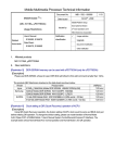
Application Note
Multimedia Processor for Mobile Applications
Initialization
--------------------------------------------------------------------------------------
EMMA Mobile1
Document No.
Date Published
S19897EJ1V0AN00
Aug 2009
2009
Printed in Japan
PREFACE
PREFACE
Purpose
The purpose of this document is to introduce the initialization process of
EMMA mobile1, specify the usage of the system control unit (ASMU) and
the general-purpose I/O interface (GIO).
Organization
This document includes the following:
Introduction
Initialization Function
Usage of ASMU Interface
Usage of GIO Interface
Example of ASMU Operation
Example of GIO Operation
ASMU Driver Function
GIO Driver Function
Notation
Here explains the meaning of following words in text:
Related document
Note
Explanation of item indicated in the text
Caution
Information to which user should afford special attention
Remark
Supplementary information
The following tables list related documents.
Reference Document
Document Name
Version/date
Author
S19265EJ1V0UM00_ASMUGIO.pdf
1st edition
NECEL
S19268EJ1V0UM00_1chip.pdf
S19254EJ1V0UM00_DDR.pdf
S19262EJ1V0UM00_UART.pdf
S19907EJ1V0AN00_GD.pdf
DDI0301G_arm1176jzfs_r0p7_trm.pdf
1st edition
1st edition
1st edition
1st edition
rp07
NECEL
NECEL
NECEL
NECEC
ARM
Description
ASMU/GIO User’s
Manual
1 Chip User’s Manual
DDR User’s Manual
UART User’s Manual
GD Spec
ARM User’s Manual
Note: ARM is “Advanced RISC Machines”. The “DDI0301G_arm1176jzfs_r0p7_trm.pdf” can be
downloaded at “ http://infocenter.arm.com/help/index.jsp?topic=/com.arm.doc.set.arm11/ “.
Application Note S19897EJ1V0AN00
PREFACE
Disclaimers
The information contained in this document is subject to change without prior
notice in the future. Refer to the latest applicable data sheet(s) and user’s manual
when designing a product for mass production.
No part of this document may be copied or reproduced in any form or by any means
without the prior written consent of NEC Electronics. NEC Electronics assumes no
responsibility for any errors that may appear in this document.
NEC Electronics does not assume any liability for infringement of patents, copyrights or
other intellectual property rights of third parties by or arising from the use of NEC
Electronics products listed in this documents or any other liability arising from the use of
such products. No license, express, implied or otherwise, is granted under any patents,
copyrights or other intellectual property rights of NEC Electronics or others.
Descriptions of circuits, software and other related information in this document are
provided for illustrative purposes in semiconductor product operation and application
examples. The incorporation of these circuits, software and information in the design of a
customers’ equipment shall be done under the full responsibility of the customer. NEC
Electronics assume no responsibility for any losses incurred by customers or third parties
arising from the use of these circuits, software and information.
While NEC Electronics endeavors to enhance the quality, reliability and safety of NEC
Electronics products, customers agree and acknowledge that possibility of defects thereof
cannot be eliminated entirely. To minimize risks of damage to property or injury (including
death) to persons arising from defects in NEC Electronics products, customers must
incorporate sufficient safety measures in their design, such as redundancy, firecontainment and anti-failure features.
Note)
1.
“NEC Electronics” as used in this document means NEC Electronics Corporation and also
includes its majority-owned subsidiaries.
2.
“NEC Electronics products” means any product developed or manufactured by or for NEC
Electronics (as defined above)
3.
All trademarks or registered trademarks are the property of their respective owners.
Registered trademarks ® and trademarks™ are not noted in this document.
Application Note S19897EJ1V0AN00
INDEX
4/84
CONTENTS
Chapter 1 Introduction ...................................................................................................................... 8
1.1 Outline........................................................................................................................................ 8
1.2 Development Environment ........................................................................................................ 8
Chapter 2 Initialization Function ...................................................................................................... 9
2.1 EMMA Mobile1 Boot Flow.......................................................................................................... 9
2.2 Operation Detail ........................................................................................................................11
2.3 The EMMA Mobile1 State after Initialization ............................................................................ 16
2.4 Boot Mode and Memory Map .................................................................................................. 18
2.4.1 Boot Mode ..................................................................................................................... 18
2.4.2 Memory Map.................................................................................................................. 19
Chapter 3 Usage of ASMU Interface............................................................................................... 20
3.1 Set Reset ................................................................................................................................. 20
3.2 Set Clock Gate......................................................................................................................... 20
3.3 Set Automatic Clock Gate........................................................................................................ 20
3.4 Set Divisor................................................................................................................................ 21
3.5 Set Automatic Frequency......................................................................................................... 21
Chapter 4 Usage of GIO Interface .................................................................................................. 22
4.1 Set the Output.......................................................................................................................... 23
4.2 Get the Input ............................................................................................................................ 24
4.3 Enable the Interrupt ................................................................................................................. 25
Chapter 5 Example of ASMU Operation.......................................................................................... 27
5.1 Example of Set the Reset State............................................................................................... 27
5.1.1 Operation Flow .............................................................................................................. 27
5.1.2 Operation Detail............................................................................................................. 28
5.2 Example of Set the Clock Gate................................................................................................ 29
5.2.1 Operation Flow .............................................................................................................. 29
5.2.2 Operation Detail............................................................................................................. 30
5.3 Example of Set the Automatic Clock Gate............................................................................... 31
5.3.1 Operation Flow .............................................................................................................. 31
5.3.2 Operation Detail............................................................................................................. 32
5.4 Example of Set Divisor Parameter .......................................................................................... 33
5.4.1 Operation Flow .............................................................................................................. 33
5.4.2 Operation Detail............................................................................................................. 34
Chapter 6 Example of GIO Operation ............................................................................................. 35
6.1 Example of Set the Output....................................................................................................... 35
Application Note S19897EJ1V0AN00
INDEX
5/84
6.1.1 Operation Flow .............................................................................................................. 36
6.1.2 Operation Detail............................................................................................................. 37
6.2 Example of Set the Input ......................................................................................................... 38
6.2.1 Operation Flow .............................................................................................................. 39
6.2.2 Operation Detail............................................................................................................. 40
6.3 Example of Enable the Interrupt .............................................................................................. 42
6.3.1 Operation Flow .............................................................................................................. 43
6.3.2 Operation Detail............................................................................................................. 44
Appendix A ASMU Driver Function ................................................................................................ 46
A.1 ASMU Driver Function List ...................................................................................................... 46
A.2 ASMU Driver Function Detail................................................................................................... 47
A.2.1 Set the Reset State ....................................................................................................... 47
A.2.2 Get the Reset State....................................................................................................... 50
A.2.3 Set the Clock Gate ........................................................................................................ 52
A.2.4 Get the Clock Gate........................................................................................................ 54
A.2.5 Set the Clock Automatic Gate ....................................................................................... 56
A.2.6 Get the Clock Automatic Gate....................................................................................... 58
A.2.7 Set the Peripheral Device Divisor ................................................................................. 60
A.2.8 Get the Peripheral Device Divisor................................................................................. 62
A.2.9 Change the Divisor Parameter to Register Value ......................................................... 64
Appendix B GIO Driver Function.................................................................................................... 65
B.1 GIO Driver Function List.......................................................................................................... 65
B.2 GIO Global Variable Define ..................................................................................................... 66
B.3 GIO Structure Define ............................................................................................................... 67
B.3.1 st_GPIO_SETTING....................................................................................................... 67
B.4 GIO Driver Function Detail ...................................................................................................... 68
B.4.1 Initialize the GIO............................................................................................................ 68
B.4.2 Alternate the Port .......................................................................................................... 70
B.4.3 Set the Port Configure................................................................................................... 71
B.4.4 Get the Port Configure .................................................................................................. 73
B.4.5 Write Data to Port.......................................................................................................... 74
B.4.6 Read Data from Port ..................................................................................................... 76
B.4.7 Enable Port Interrupt ..................................................................................................... 77
B.4.8 Disable Port Interrupt .................................................................................................... 81
B.4.9 Interrupt Handler ........................................................................................................... 82
ANNEX Modification History............................................................................................................ 84
Application Note S19897EJ1V0AN00
INDEX
6/84
LIST OF TABLES
Table 1-1 Hardware Environment ....................................................................................... 8
Table 1-2 Software Environment......................................................................................... 8
Table 2-1 Process Necessity ............................................................................................ 10
Table 2-2 Device Reset State Table ................................................................................. 16
Table 2-3 Device Clock Gate Table .................................................................................. 16
Table 2-4 PLL Frequency.................................................................................................. 17
Table 2-5 Clock Frequency ............................................................................................... 17
Table 2-6 Boot Mode......................................................................................................... 18
Table 2-7 Memory Map ..................................................................................................... 19
Table A-1 ASMU Driver Function List ............................................................................... 46
Table B-1 GIO Driver Function List ................................................................................... 65
Table B-2 Global Variable Define...................................................................................... 66
Table B-3 Structure Define................................................................................................ 67
Table B-4 Structure of st_GPIO_SETTING ...................................................................... 67
LIST OF FIGURES
Figure 2-1 System Initialize Process Flow .......................................................................... 9
Figure 4-1 GIO Outputy................................................................................................... 23
Figure 4-2 GIO Input ......................................................................................................... 24
Figure 4-3 GIO Interrupt.................................................................................................... 25
Figure 5-1 Set the Reset State.......................................................................................... 27
Figure 5-2 Set the Clock Gate........................................................................................... 29
Figure 5-3 Set the Automatic Clock Gate ......................................................................... 31
Figure 5-4 Set the Divisor Parameter................................................................................ 33
Figure 6-1 Hardware Connection of GIO 1 Output ........................................................... 35
Figure 6-2 Set the Output.................................................................................................. 36
Figure 6-3 Hardware Connection of GIO 1 and GIO 7...................................................... 38
Figure 6-4 Set the Input .................................................................................................... 39
Figure 6-5 The Hardware Connnection without Synchronous High Interrupt ................... 42
Figure 6-6 The Hardware Connnection with Synchronous High Interrupt ........................ 42
Figure 6-7 Enable the Interrupt ......................................................................................... 43
Figure A-1 Set the Reset State ......................................................................................... 48
Figure A-2 Get the Reset State......................................................................................... 51
Application Note S19897EJ1V0AN00
INDEX
7/84
Figure A-3 Set the Clock Gate .......................................................................................... 52
Figure A-4 Get the Clock Gate.......................................................................................... 54
Figure A-5 Set the Clock Automatic Gate ......................................................................... 57
Figure A-6 Get the Clock Automatic Gate......................................................................... 59
Figure A-7 Set the Device Divisor ..................................................................................... 61
Figure A-8 Get the Device Divisor..................................................................................... 63
Figure B-1 GIO Initialize.................................................................................................... 69
Figure B-2 GIO Alternate .................................................................................................. 70
Figure B-3 Set the GIO Configure..................................................................................... 72
Figure B-4 Get the GIO Configure .................................................................................... 73
Figure B-5 Write Data ....................................................................................................... 74
Figure B-6 Read Data ....................................................................................................... 76
Figure B-7 Enable the GIO Interrupt (1)............................................................................ 78
Figure B-8 Enable the GIO Interrupt (2)............................................................................ 79
Figure B-9 Disable the GIO Interrupt ................................................................................ 81
Figure B-10 The Interrupt Handler of GIO 0 -31 ............................................................... 82
Application Note S19897EJ1V0AN00
Chapter 1 Introduction
8/84
Chapter 1 Introduction
1.1 Outline
This document introduces three parts: initialization, the system control unit (ASMU) and the generalpurpose I/O interface (GIO) of EMMA Mobile1.
(1). Initialization.
How to set device reset state, stack address, interrupt handler, memory, clock and UART;
(2). ASMU.
How to reset the device;
How to open or close the clock gate;
How to open or close the automatic clock gate;
How to set the divisor parameter;
(3). GIO.
How to output data;
How to input data;
How to set GIO interrupt;
1.2 Development Environment
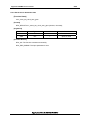
Hardware environment of this project is listed as below.
Table 1-1 Hardware Environment
Name
Version
Maker
EMMA Mobile1 evaluation board (PSKCH2YS-0016-01)
-
NEC Electronics
M20
Kyoto Microcomputer Co. Ltd
PARTNER-Jet ICE ARM
Software used in this project is listed as below.
Table 1-2 Software Environment
Version
Maker
GNUARM Toolchain
Name
V4.3.2
GNU
WJETSET-ARM
V5.10a
Kyoto Microcomputer Co. Ltd
Application Note S19897EJ1V0AN00
Chapter 2 Initialization Function
9/84
Chapter 2 Initialization Function
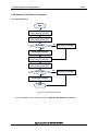
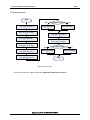
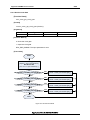
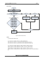
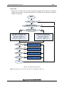
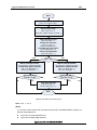
2.1 EMMA Mobile1 Boot Flow
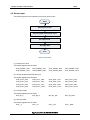
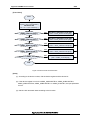
The boot program executes as following figure.
Power on
Enable Instruction cache
Set BSS segment
Set the clock gate
Reset release the device
assembler
initialize
Set stack address
Initialize interrupt
Set fatal error loop
Go to main
C initialize
Set DDR SDRAM
Set system clock
Set UART
EMMA Mobile1 enters
normal state
Figure 2-1 System Initialize Process Flow
Application Note S19897EJ1V0AN00
Chapter 2 Initialization Function
10/84
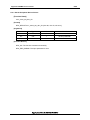
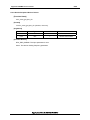
But some progress is not necessary in the initialization, please refer to the following table:
Table 2-1 Process Necessity
Process
Necessity
Enable Instruction cache
No
Set BSS segment
Set the clock & Reset release the device
Set stack address
Initialize interrupt
Set fatal error loop
Yes
Yes
Yes
Yes
Yes
Go to main
Set DDR SDRAM
Set system clock
Set UART
Yes
Yes
Yes
No
Application Note S19897EJ1V0AN00
Chapter 2 Initialization Function
11/84
2.2 Operation Detail
The following steps describe the figure 2-1 processes.
(1) Enable instruction cache.
The EMMA Mobile1 has separate instruction cache (32 KB) and data cache (32 KB). In c1
register of P15, the bit[12] controls the instruction cache enable or not. If the bit[12] is 1, enable
the instruction cache. If the bit[12] is 0, disable the instruction cache.
About the details, please refer to the ARM user’s manual.
(
// Get the c1 of P15 to r1.
mrc
p15, 0, r1, c1, c0, 0
// Set the r1[12] to 1. Enable the instruction cache
orr
r1, r1, #0x1000
// Set the r1 to c1 of p15.
mcr
p15, 0, r1, c1, c0, 0
)
(2) Set BSS segment.
The data_end is the start address of BSS and the bss_end is the end address of BSS.
About the “data_end” and “bss_end” details, please refer to the rom_ld.script and rom_start.S
files.
{
// Load the data_end value to r1.
ldr
r1, data_end
// Load the bss_end value to r2.
ldr
r2, bss_end
// Se the r3 to 0.
mov
r3, #0
1:
// Compare r1 and r2.
cmp
r1, r2
// If r1 is smaller than r2, store r3’s value to the address indicated by r1, then add 4 to r1.
strcc
r3, [r1], #4
Application Note S19897EJ1V0AN00
Chapter 2 Initialization Function
12/84
// If r1 is smaller than r2, move the PC (program counter) to the back label 1.
bcc
1b
}
(3) Set the clock & Reset release the device.
If the device is reset, it can not be used. If the clock gate is closed, the device does not have
clock.
// Open U70 SCLK
ASMU_GCLKCTRL2_ENA[6] = 1;
ASMU_GCLKCTRL2[6] = 1;
ASMU_GCLKCTRL2_ENA[6] = 0;
// Reset release U70
ASMU_RESETREQ0_ENA[27] = 1;
ASMU_RESETREQ0[27] = 1;
ASMU_RESETREQ0_ENA[27] = 0;
// Reset U71
ASMU_RESETREQ0_ENA[28] = 1;
ASMU_RESETREQ0[28] = 0;
ASMU_RESETREQ0_ENA[28] = 0;
// Close the U71 SCLK
ASMU_GCLKCTRL2_ENA[7] = 1;
ASMU_GCLKCTRL2[7] = 0;
ASMU_GCLKCTRL2_ENA[7] = 0;
U70 and U71 are only two examples. About the register definition, please refer to the ASMU/GIO
user’s manual. About the details of reset and clock, please refer to the source code of rom_start.S
file.
(4) Set the stack address.
The ARM has 7 running modes. IRQ and SVC are only two running modes. This step sets stack
base address of IRQ mode and SVC mode.
The CPSR is “Current Program Status Register”. The meaning of lower 6 bits is as follow:
CPSR[5] = 1, undefined instruction interrupt ;
CPSR[5] = 0, execute ARM instruction.
CPSR[4:0] = 0x10 : User mode;
CPSR[4:0] = 0x11 : FIQ mode;
CPSR[4:0] = 0x12 : IRQ mode;
CPSR[4:0] = 0x13 : Supervisor mode;
CPSR[4:0] = 0x17 : Abort mode;
Application Note S19897EJ1V0AN00
Chapter 2 Initialization Function
13/84
CPSR[4:0] = 0x1B : Undefined mode;
CPSR[4:0] = 0x1F : System mode;
About the ARM details, please refer to the ARM user’s manual.
{
#define SUB_IRQ_STACK
0x0
#define SUB_SVC_STACK
0x200
// Load the stack_base value to r1, stack_base is the stack base address.
ldr
r1, stack_base
// Disable FIQ and IRQ interrupt. Enter IRQ mode.
msr
CPSR_c, #0xd2
// Reduce SUB_IRQ_STACK from r1, then set the result to sp (stack pointer) in IRQ mode.
sub
sp, r1, #SUB_IRQ_STACK
// Disable FIQ and IRQ interrupt. Enter SVC mode.
msr
CPSR_c, #0xd3
// Reduce SUB_SVC_STACK from r1, then set the result to sp (stack pointer) in SVC mode.
sub
sp, r1, #SUB_SVC_STACK
}
(5) Initialize the interrupt.
The CPSR is “Current Program Status Register”. The bit 6 and bit 7 definitions are as follow:
CPSR[7] = 1, disable the IRQ interrupt ; CPSR[7] = 0, enable the IRQ interrupt.
CPSR[6] = 1, disable the FIQ interrupt ; CPSR[6] = 0, enable the FIQ interrupt.
{
// Store the IRQ interrupt handler function address irq_jump_addr to the SRAM
irq_jump_sram_addr.
ldr
r1, irq_jump_sram_addr
ldr
r2, irq_jump_addr
str
r2, [r1]
// Store the SWI interrupt handler function address swi_jump_addr to the SRAM
swi_jump_sram_addr.
ldr
r1, swi_jump_sram_addr
ldr
r2, swi_jump_addr
str
r2, [r1]
// Store the FIQ interrupt handler function address fiq_jump_addr to the SRAM
Application Note S19897EJ1V0AN00
Chapter 2 Initialization Function
14/84
fiq_jump_sram_addr.
ldr
r1, fiq_jump_sram_addr
ldr
r2, fiq_jump_addr
str
r2, [r1]
// Enter interrupt initialize function, disable the IRQ and FIQ.
bl
intr_init
// Load the CPSR to r1.
mrs
r1, CPSR
// Set bit 7 to 0 in r1.
bic
r1, r1, #0x80
// Store r1 to CPSR, enable IRQ interrupt.
msr
CPSR_c, r1
}
(6) Set the fatal error loop.
This step initializes the error loop address.
About the details, please refer to the 1 Chip user’s manual.
{
// Store the error loop function address fatal_err_loop to the SRAM fatal_err_sram_addr.
ldr
r1, fatal_err_sram_addr
ldr
r2, fatal_err_loop
str
r2, [r1]
}
(7) Go to the main function.
{
// Jump to the c main function
bl
em1_eva_main
}
(8) Set the DDR SDRAM.
This function initializes the DDR SDRAM.
About the register definition, please refer to the ASMU/GIO user’s manual, DDR user’s manual
and 1 Chip user’s manual.
About how to initialize the DDR SDRAM, please refer to the source code of em1_driver_ddr.c file.
Application Note S19897EJ1V0AN00
Chapter 2 Initialization Function
15/84
(9) Set the clock.
This function sets the frequency of ACPU, ADSP, HBUS, LBUS, FLASH and MEMC.
About the register definition, please refer to the ASMU/GIO user’s manual.
About how to set the clock frequency, please refer to the source code of em1_driver_ddr.c file.
(10) Set the UART.
This function sets the UART0 and the UART0 is used for send and receive characters with PC.
About the register definition, please refer to the UART user’s manual, ASMU/GIO user’s manual
and 1 Chip user’s manual.
About how to initialize the UART0, please refer to the source code of em1_driver_uart.c file.
Application Note S19897EJ1V0AN00
Chapter 2 Initialization Function
16/84
2.3 The EMMA Mobile1 State after Initialization
The following table shows the device reset state. If the device resets off, it can be used. If the
device resets on, it can not be used.
Table 2-2 Device Reset State Table
Reset
Device
OFF
MEMC, U70, GIO, AINT, SRC, PB1, PB0, AB1, AB0, ACPU_ATRST,
ACPU_PORST, ACPU_RST, CHG, SHXB, DXHB, MHXB, SWL1, SWL0, AXL1,
AXL0.
ON
ADSP, U72, U71, NTS, DTV, IMC, AVC, DMA, LCD, IPUAHB, IPUDMA, IPUROT,
IPUIMG, DCV, ADSP_SRST, ADSP_ARST, MMM, MSP, USB, NAND, IIC, IIC2,
SP2, SP1, SP0, MWI, PDMA, PM1, PM0, TG5, TG4, TG3, TG2, TG1, TG0,
TW3, TW2, TW1, TW0, TI3, TI2, TI1, TI0, PMU, PWM, TW3_RSTREQ,
TW0_RSTREQ, ADSP_WDTRST_MODE, ACPU_WDTRST_MODE,
ADSP_WDTRST, ACPU_WDTRST, SDICRSTZ, SDIBRSTZ, SDIARSTZ,
DTV_SAFE, USB_SAFE.
The following table shows the clock gate state. If the clock is on, the device has the clock supply.
If the clock is off, the device doesn’t have the clock supply.
Table 2-3 Device Clock Gate Table
Clock
ON
OFF
Device
AB1_CLK, PB0_CLK, AXL1_PMON_CLK, MHXB_CLK, DHXB_CLK, SWL1_CLK,
AXL1_PCLK, AXL1_CLK, CHG_PCLK, AINT_PCLK, SRC_CLK, MEMC_RCLK,
MEMC_PCLK, MEMC_CLK270_GCK, MEMC_CLK, SWL0_CLK, AXL0_PCLK,
AXL_CLK, SHXB_HCLK, SHXB_CLK, U70_SCLK, U70_CLK.
DMA_TCLK, DMA_PCH3_CLK, DMA_PCH2_CLK, DMA_PCH0_CLK,
DMA_PCLK_GCK, IMC_PCLK, IMC_CLK, IPUAHB_CLK, IPUDMA_PCLK,
IPUDMA_CLK, IPUROT_PCLK, IPUROT_CLK, IPUIMG_PCLK, IPUIMG_2_CLK,
IPUIMG_1_CLK, PDMA_PCLK, PDMA_HCLK, PDMA_ACLK, ADSP_ACLK,
ADSP_CLK, AVC_HSCLK, AVC_HMCLK, AVC_CLKM, AVC_CLKE, AVC_CLKD,
AVC_CLKC, DCV_PCLK, DCV_CLK, LCD_CCLK, LCD_LCLK, LCD_PCLK,
LCD_CLK, DTV_PCLK, DTV_CLK, NTS_PCLK, NTS_CLK, NAND_PCLK,
NAND_HCLK, REF_CLK, MSP_RTCK, MSP_SCLK, MSP_PCLK, MMM_CLK,
PM1_SCLK, PM0_SCLK, PM0_PCLK, USB_CLK, U72_SCLK, U71_SCLK,
IIC_SCLK, IIC_CLK, IIC2_SCLK, IIC2_CLK, FLASHCLK, EFS_PCLK,
PWM_PWCLK1, PWM_PWCLK0, PWM_PCLK, SP2_SCLK, SP2_PCLK,
SP1_SCLK, SP1_PCLK, SP0_SCLK, SP0_PCLK, MWI_SCLK, MWI_PCLK,
ATIM_PCLK, TW3_TIN, TW2_TIN, TW1_TIN, TW0_TIN, TG5_TIN, TG4_TIN,
TG3_TIN, TG2_TIN, TG1_TIN, TG0_TIN, TI3_TIN, TI2_TIN, TI1_TIN, TI0_TIN.
Application Note S19897EJ1V0AN00
Chapter 2 Initialization Function
17/84
When the EMMA Mobile1 enters the normal A state, the PLL1, PLL2 and PLL3 are as following table:
Table 2-4 PLL Frequency
PLL
PLL1
PLL2
PLL3
Frequency
499.712 MHz
499.712 MHz
229.376 MHz
Note: The PLL1 is set in the “Set the DDR SDRAM” process of figure 2-1. The PLL2 and PLL3
use the default value. About how to set PLL2 and PLL3, please refer to the PLL1.
When the EMMA Mobile1 enters the normal A state, the frequency are as following table:
Table 2-5 Clock Frequency
Module
ACPU
ADSP
HBUS
LBUS
FLASH
MEMC
Frequency
500MHz
500MHz
166MHz
83.3MHz
83.3MHz
166MHz
Note:
(1). Make sure that the divided domain clock frequencies satisfy the following condition.
ACPU, ADSP >= MEMC >= HBUS >= FLASH, LBUS
In addition, specify the frequency of each domain clock so as to be a multiple of an integer.
(2). Maximum frequency of each domain clock (PLL1 = 500 MHz)
ACPU: 500 MHz;
ADSP: 500 MHz;
HBUS: 166.6 MHz;
LBUS: 83.3 MHz;
FLASH: 83.3 MHz;
MEMC: 166.6 MHz;
Application Note S19897EJ1V0AN00
Chapter 2 Initialization Function
18/84
2.4 Boot Mode and Memory Map
2.4.1 Boot Mode
The DSW2 of “EM1_Evaluation Board (PSKCH2Y-S-0016-01)” controls the boot mode. The
relationship between DSW2 and BOOTSEL is as follow:
DSW2-1 < - > BOOTSEL3;
DSW2-2 < - > BOOTSEL2;
DSW2-3 < - > BOOTSEL1;
DSW2-4 < - > BOOTSEL0;
The boot mode is decided by BOOTSEL, please refer to the following table. “ADSP JTAG” is used for
ADSP mode. About the details of table 2-6, please refer to the 1 Chip user’s manual.
Table 2-6 Boot Mode
Process
BOOT_SEL3
BOOT_SEL[2:0]
Necessary
Switching to L_SPEED mode (low-speed clock mode)
000:
001:
010:
011:
100:
101:
110:
111:
AB0 boot
eMMC boot
SD boot
MS boot (SD0 port)
NAND boot
AB0 boot (ADSP JTAG)
eMMC boot (ADSP JTAG)
SD boot (ADSP JTAG)
This example boots from Nor Flash, so the DSW2-1, DSW2-2, DSW2-3 and DSW2-4 should be set
to OFF.
Application Note S19897EJ1V0AN00
Chapter 2 Initialization Function
19/84
2.4.2 Memory Map
The following table is the memory map table:
Table 2-7 Memory Map
Content
Source code
Global and local static data
Stack and interrupt jump vectors
Device
Start Address
End Address
Nor Flash
DDR SDRAM
0x00000000
0x33000000
0x01FFFFFF
0x33FFFFFF
SRAM
0xA0001000
0xA001FFFF
The follow example sets the code to the memory addressed 0x00000000.
SECTIONS
{
. = 0x00000000 ;
/* Start memory address
*/
.text : {
/* Real text segment
*/
/* Text
*/
/* End of text section
*/
_text = .;
*(.text)
_etext = .;
}
}
About the details of memory allocation please refer to the rom_ld.script file.
Application Note S19897EJ1V0AN00
Chapter 3 Usage of ASMU Interface
20/84
Chapter 3 Usage of ASMU Interface
According to the hardware feature, the ASMU can have the following function:
(1). Set reset state.
(2). Set clock gate.
(3). Set automatic clock gate.
(4). Set divisor.
(5). Set automatic frequency.
3.1 Set Reset
(1). Set reset state.
If reset the device, the device can not be used. If reset release the device, the device can be
used. The related registers are as follow (Note: x is 0, 1 or 2, 3):
ASMU_RESETREQxENA;
ASMU_RESETREQx;
ASMU_DTV_SAFE_RESET;
ASMU_USB_SAFE_RESET;
3.2 Set Clock Gate
(1). Set clock gate.
If open the clock gate, the device can be supplied with clock. If close the clock gate, the device
can not be supplied with clock. The related registers are as follow (Note: x is 0, 1 or 2, 3):
ASMU_GCLKCTRLxENA;
ASMU_GCLKCTRLx;
ASMU_GCLKCTRLxENA;
3.3 Set Automatic Clock Gate
(1). Set automatic clock gate.
When open the automatic clock gate of a device, if the device does not have clock request, the
clock used by the device is not supplied. The related registers are as follow:
ASMU_AHBCLKCTRL0;
ASMU_AHBCLKCTRL1;
ASMU_APBCLKCTRL0;
ASMU_APBCLKCTRL1;
ASMU_CLKCTRL;
Application Note S19897EJ1V0AN00
Chapter 3 Usage of ASMU Interface
21/84
3.4 Set Divisor
(1). Set divisor.
When use a device, clock divisor should be set for a specified clock frequency. The related
registers are as follow:
ASMU_DIVMSPSCLK;
ASMU_DIVSP0SCLK;
ASMU_DIVSP1SCLK;
ASMU_DIVSP2SCLK;
ASMU_DIVMEMCRCLK;
ASMU_DIVLCDLCLK;
ASMU_DIVIICSCLK;
ASMU_DIVTIMTIN;
ASMU_DIVMWISCLK;
ASMU_DIVDMATCLK;
ASMU_DIVU70SCLK;
ASMU_DIVU71SCLK;
ASMU_DIVU72SCLK;
ASMU_DIVPM0SCLK;
ASMU_DIVPM1SCLK;
ASMU_DIVPWMPWCLK;
3.5 Set Automatic Frequency
(1). Set automatic frequency.
When enable the automatic frequency of a device, if the device does not have clock request, the
clock used by the device is decreased. The related registers are as follow:
ASMU_CLK_MODE_SEL;
ASMU_NORMALA_DIV;
ASMU_NORMALB_DIV;
ASMU_NORMALC_DIV;
ASMU_NORMALD_DIV;
ASMU_POWERON_DIV;
ASMU_AUTO_FRQ_CHANGE;
ASMU_AUTO_FRQ_MASK0;
ASMU_AUTO_FRQ_MASK1;
And there is no example about this setting in the chapter 5.
Application Note S19897EJ1V0AN00
Chapter 4 Usage of GIO Interface
Chapter 4 Usage of GIO Interface
According to the hardware feature, the GIO can have the following function:
(1). Output to a port.
(2). Input from a port.
(3). Wait the interrupt on a port.
Application Note S19897EJ1V0AN00
22/84
Chapter 4 Usage of GIO Interface
23/84
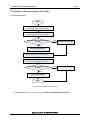
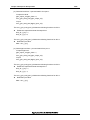
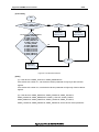
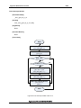
4.1 Set the Output
The following picture is the operation process for set the output.
Start
Switch port to GIO
Set pull-up/pull-down/mask-input
Set output mode
Set output data
End
Figure 4-1 GIO Output
(1). Switch port to GIO.
The related registers are as follow:
CHG_PINSEL_G00;
CHG_PINSEL_G16;
CHG_PINSEL_G32;
CHG_PINSEL_G48;
CHG_PINSEL_G64;
CHG_PINSEL_G80;
CHG_PINSEL_G96;
CHG_PINSEL_G112;
(2). Set pull up/pull down/mask the input.
The related registers are as follow:
CHG_PULL_G00;
CHG_PULL_G08;
CHG_PULL_G16;
CHG_PULL_G24;
CHG_PULL_G32;
CHG_PULL_G40;
CHG_PULL_G48;
CHG_PULL_G56;
CHG_PULL_G64;
CHG_PULL_G72;
CHG_PULL_G80;
CHG_PULL_G88;
CHG_PULL_G96;
CHG_PULL_G104;
CHG_PULL_G112;
CHG_PULL_G120;
GIO_E1_HH;
GIO_E1_HHH;
(3). Set output mode.
The related registers are as follow:
GIO_E1_L;
GIO_E1_H;
(4). Set output data.
The related registers are as follow:
GIO_OL_L;
GIO_OH_L;
GIO_OL_H;
GIO_OH_H;
GIO_OL_HH;
GIO_OH_HH;
GIO_OL_HHH;
GIO_OH_HHH;
Application Note S19897EJ1V0AN00
Chapter 4 Usage of GIO Interface
24/84
4.2 Get the Input
The following picture is the operation process for get the input.
Start
Switch port to GIO
Set pull-up/pull-down/mask-input
Set input mode
Get input data
End
Figure 4-2 GIO Input
(1). Switch port to GIO.
The related registers are as follow:
CHG_PINSEL_G00;
CHG_PINSEL_G16;
CHG_PINSEL_G32;
CHG_PINSEL_G48;
CHG_PINSEL_G64;
CHG_PINSEL_G80;
CHG_PINSEL_G96;
CHG_PINSEL_G112;
(2). Set pull up/pull down/mask the input.
The related registers are as follow:
CHG_PULL_G00;
CHG_PULL_G08;
CHG_PULL_G16;
CHG_PULL_G24;
CHG_PULL_G32;
CHG_PULL_G40;
CHG_PULL_G48;
CHG_PULL_G56;
CHG_PULL_G64;
CHG_PULL_G72;
CHG_PULL_G80;
CHG_PULL_G88;
CHG_PULL_G96;
CHG_PULL_G104;
CHG_PULL_G112;
CHG_PULL_G120;
GIO_E0_HH;
GIO_E0_HHH;
GIO_I_HH;
GIO_I_HHH;
(3). Set input mode.
The related registers are as follow:
GIO_E0_L;
GIO_E0_H;
(4). Get input data.
The related registers are as follow:
GIO_I_L;
GIO_I_H;
Application Note S19897EJ1V0AN00
Chapter 4 Usage of GIO Interface
25/84
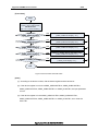
4.3 Enable the Interrupt
The following picture is the operation process for enable the interrupt.
Start
Switch pin to GIO
Set pull-up/pull-down/mask-input
Set input mode
Set interrupt detection mode
Clear interrupt source
Enable GIO interrupt
Send GIO_INT_FIQ signal
Disable interrupt mask
Enable GIO global interrupt
End
Figure 4-3 GIO Interrupt
(1). Switch port to GIO.
The related registers are as follow:
CHG_PINSEL_G00;
CHG_PINSEL_G16;
CHG_PINSEL_G32;
CHG_PINSEL_G48;
CHG_PINSEL_G64;
CHG_PINSEL_G80;
CHG_PINSEL_G96;
CHG_PINSEL_G112;
(2). Set pull up/pull down/mask the input.
The related registers are as follow:
Application Note S19897EJ1V0AN00
Chapter 4 Usage of GIO Interface
26/84
CHG_PULL_G00;
CHG_PULL_G08;
CHG_PULL_G16;
CHG_PULL_G24;;
CHG_PULL_G32;
CHG_PULL_G40;
CHG_PULL_G48;
CHG_PULL_G56;
CHG_PULL_G64;
CHG_PULL_G72;
CHG_PULL_G80;
CHG_PULL_G88;
CHG_PULL_G96;
CHG_PULL_G104;
CHG_PULL_G112;
CHG_PULL_G120;
GIO_E0_HH;
GIO_E0_HHH;
(3). Set input mode.
The related registers are as follow:
GIO_E0_L;
GIO_E0_H;
(4). Set interrupt detection mode.
The related registers are as follow:
GIO_IDT0_L;
GIO_IDT1_L;
GIO_IDT2_L;
GIO_IDT3_L;
GIO_IDT0_H;
GIO_IDT1_H;
GIO_IDT2_H;
GIO_IDT3_H;
GIO_IDT0_HH;
GIO_IDT1_HH;
GIO_IDT2_HH;
GIO_IDT3_HH;
GIO_IDT0_HHH;
GIO_IDT1_HHH;
GIO_IDT2_HHH;
GIO_IDT3_HHH
GIO_IIR_HH;
GIO_IIR_HHH;
GIO_IIA_HH;
GIO_IIA_HHH;
GIO_GSW_HH;
GIO_GSW_HHH;
GIO_IEN_HH;
GIO_IEN_HHH;
(5). Clear interrupt source.
The related registers are as follow:
GIO_IIR_L;
GIO_IIR_H;
(6). Enable GIO interrupt.
The related registers are as follow:
GIO_IIA_L;
GIO_IIA_H;
(7). Send FIQ signal.
The related registers are as follow:
GIO_GSW_L;
GIO_GSW_H;
(8). Disable interrupt mask.
The related registers are as follow:
GIO_IEN_L;
GIO_IEN_H;
(9). Enable GIO global interrupt.
The related registers are as follow:
SEC_IT0_IENS0;
INTC_IT0_IEN0;
SEC_IT0_IENS1;
INTC_IT0_IEN1;
SEC_IT0_IENS2;
INTC_IT0_IEN2;
Application Note S19897EJ1V0AN00
Chapter 5 Example of ASMU Operation
27/84
Chapter 5 Example of ASMU Operation
The following contents show 4 examples: how to set the reset state, how to set the clock, how to
set the automatic clock gate and how to set the device divisor parameter. About the API details,
please refer to the “Appendix A ASMU Driver Function”.
5.1 Example of Set the Reset State
5.1.1 Operation Flow
Start
Set IIC reset OFF
[em1_asmu_set_reset; ]
Get IIC reset state
[ em1_asmu_get_reset; ]
IIC reset state == OFF?
No
Printf error message
Yes
Printf the right message
Set IIC reset ON
[em1_asmu_set_reset; ]
Get IIC reset state
[ em1_asmu_get_reset; ]
IIC reset state == ON?
No
Printf error message
Yes
Printf right message
End
Figure 5-1 Set the Reset State
About the ASMU function, please refer to the “Appendix A ASMU Driver Function”
Application Note S19897EJ1V0AN00
Chapter 5 Example of ASMU Operation
28/84
5.1.2 Operation Detail
(1). Set the IIC reset off, then get the IIC reset state. Judge the new reset state of IIC is off or not.
// “0x00030000|26” is IIC device index, 0 is off.
em1_asmu_set_reset (0x00030000|26, 0);
state = em1_asmu_get_reset (0x00030000|26);
The em1_asmu_set_reset () finishes the following functions for IIC:
Enable write the reset bit.
ASMU_RESETREQ1ENA[26] = 1;
Set the reset state.
ASMU_RESETREQ1[26] = 1;
Disable write the reset bit.
ASMU_RESETREQ1ENA[26] = 0;
The em1_asmu_get_reset () finishes the following functions for IIC:
Get the reset state.
state = ASMU_RESETREQ1[26];
(2). Set the IIC reset on, then get the IIC reset state. Judge the new reset state of IIC is on or not.
// “0x00030000|26” is IIC device index, 1 is on.
em1_asmu_set_reset (0x00030000|26, 1);
state = em1_asmu_get_reset (0x00030000|26);
The em1_asmu_set_reset () finishes the following functions for IIC:
Enable write the reset bit.
ASMU_RESETREQ1ENA[26] = 1;
Set the reset state.
ASMU_RESETREQ1[26] = 0;
Disable write the reset bit.
ASMU_RESETREQ1ENA[26] = 0;
The em1_asmu_get_reset () finishes the following functions for IIC:
Get the reset state.
state = ASMU_RESETREQ1[26];
Application Note S19897EJ1V0AN00
Chapter 5 Example of ASMU Operation
29/84
5.2 Example of Set the Clock Gate
5.2.1 Operation Flow
Start
Open U71 clock gate
[ em1_asmu_set_clock_gate; ]
Get U71 clock gate state
[ em1_asmu_get_clock_gate; ]
U71 clock gate state == ON?
No
Printf error message
Yes
Printf right message
Close U71 clock gate
[ em1_asmu_set_clock_gate; ]
Get U71 clock gate state
[ em1_asmu_get_clock_gate; ]
U71 clock gate state == OFF?
No
Printf error message
Yes
Printf right message
End
Figure 5-2 Set the Clock Gate
About the ASMU function, please refer to the “Appendix A ASMU Driver Function”
Application Note S19897EJ1V0AN00
Chapter 5 Example of ASMU Operation
30/84
5.2.2 Operation Detail
(1). Open the U71 clock gate, then get the U71 clock gate state. Judge the new clock state of U71
is on or not.
// “0x000A0000|7” is U71 device index, 1 is on.
em1_asmu_set_clock_gate (0x000A0000|7, 1);
state = em1_asmu_get_clock_gate (0x000A0000|7);
The em1_asmu_set_clock_gate () finishes the following functions for U71:
Enable write the clock gate control bit.
ASMU_GCLKCTRL2ENA [7] = 1;
Set the clock gate state.
ASMU_GCLKCTRL2[7] = 1;
Disable write the clock gate control bit.
ASMU_GCLKCTRL2ENA [7] = 0;
The em1_asmu_get_clock_gate () finishes the following functions for U71:
Get the clock gate state.
state = ASMU_GCLKCTRL2[7];
(2). Close the U71 clock gate, then get the U71 clock gate state. Judge the new clock state of
U71 is off or not.
// “0x000A0000|7” is U71 device index, 0 is off.
em1_asmu_set_clock_gate (0x000A0000|7, 0);
state = em1_asmu_get_clock_gate (0x000A0000|7);
The em1_asmu_set_clock_gate () finishes the following functions for U71:
Enable write the clock gate control bit.
ASMU_GCLKCTRL2ENA [7] = 1;
Set the clock gate state.
ASMU_GCLKCTRL2[7] = 0;
Disable write the clock gate control bit.
ASMU_GCLKCTRL2ENA [7] = 0;
The em1_asmu_get_clock_gate () finishes the following functions for U71:
Get the clock gate state.
state = ASMU_GCLKCTRL2[7];
Application Note S19897EJ1V0AN00
Chapter 5 Example of ASMU Operation
31/84
5.3 Example of Set the Automatic Clock Gate
5.3.1 Operation Flow
Start
Open SP2 automatic clock
[ em1_asmu_set_clock_auto_gate; ]
Get SP2 automatic clock state
[ em1_asmu_get_clock_auto_gate; ]
SP2 automatic clock gate state
== ON?
No
Printf error message
Yes
Printf right message
Close SP2 automatic clock
[ em1_asmu_set_clock_auto_gate; ]
Get SP2 automatic clock state
[ em1_asmu_get_clock_auto_gate; ]
SP2 automatic clock gate state
== OFF?
No
Printf error message
Yes
Printf right message
End
Figure 5-3 Set the Automatic Clock Gate
About the ASMU function, please refer to the “Appendix A ASMU Driver Function”
Application Note S19897EJ1V0AN00
Chapter 5 Example of ASMU Operation
32/84
5.3.2 Operation Detail
(1). Open the SP2 automatic clock gate, then get the SP2 automatic clock gate state. Judge the
new automatic clock state of SP2 is on or not.
// “0x000E0000|7” is SP2 device index, 1 is on.
em1_asmu_set_clock_auto_gate (0x000E0000|7, 1);
state = em1_asmu_get_clock_auto_gate (0x000E0000|7);
The em1_asmu_set_clock_auto_gate () finishes the following functions for SP2:
Enable the automatic clock gate.
ASMU_APBCLKCTRL0[7] = 1;
The em1_asmu_get_clock_auto_gate () finishes the following functions for SP2:
Get the state of automatic clock gate.
state = ASMU_APBCLKCTRL0[7];
(2). Close the SP2 automatic clock gate, then get the SP2 automatic clock gate state. Judge the
new automatic clock state of SP2 is off or not.
// “0x000E0000|7” is SP2 device index, 0 is off.
em1_asmu_set_clock_auto_gate (0x000E0000|7, 0);
state = em1_asmu_get_clock_auto_gate (0x000E0000|7);
The em1_asmu_set_clock_auto_gate () finishes the following functions for SP2:
Disable the automatic clock gate.
ASMU_APBCLKCTRL0[7] = 0;
The em1_asmu_get_clock_auto_gate () finishes the following functions for SP2:
Get the state of automatic clock gate.
state = ASMU_APBCLKCTRL0[7];
Application Note S19897EJ1V0AN00
Chapter 5 Example of ASMU Operation
33/84
5.4 Example of Set Divisor Parameter
5.4.1 Operation Flow
Start
Set SP1 divisor (256)
[ em1_asmu_set_dev_div; ]
Get SP1 divisor (div)
[ em1_asmu_get_dev_div; ]
div == 256?
No
Printf error message
Yes
Printf right message
Set IIC1 divisor (128)
[ em1_asmu_set_dev_div; ]
Get IIC1 divisor (div)
[ em1_asmu_get_dev_div; ]
div == 128?
No
Printf error message
Yes
Printf right message
End
Figure 5-4 Set the Divisor Parameter
About the ASMU function, please refer to the “Appendix A ASMU Driver Function”
Application Note S19897EJ1V0AN00
Chapter 5 Example of ASMU Operation
34/84
5.4.2 Operation Detail
(1). Set the SP1 divisor parameter (256), then get the SP1 divisor parameter (div). Judge the div
is 256 or not.
// ASMU_DIVSP1SCLK is SP1 divisor register, 0xF4 is 256 divisor, 0xFF is no use.
em1_asmu_set_dev_div (ASMU_DIVSP1SCLK, 0xF4, 0xFF);
div = em1_asmu_get_dev_div (ASMU_DIVSP1SCLK, 0xFF);
The em1_asmu_set_dev_div () finishes the following functions for SP1:
Set the device divisor parameter.
ASMU_DIVSP1SCLK = 0xF4;
The em1_asmu_get_dev_div () finishes the following functions for SP1:
Get the device divisor parameter.
state = ASMU_DIVSP1SCLK;
(2). Set the IIC1 divisor parameter (128), then get the IIC1 divisor parameter (div). Judge the div
is 128 or not.
// ASMU_DIVIICSCLK is IIC1 divisor register, 0xF3 is 128 divisor, 1 is the IIC device number.
em1_asmu_set_dev_div (ASMU_DIVIICSCLK, 0xF3, 1);
div = em1_asmu_get_dev_div (ASMU_DIVIICSCLK, 1);
The em1_asmu_set_dev_div () finishes the following functions for IIC:
Set the device divisor parameter to bit[7:0] of device divisor register.
ASMU_DIVIICSCLK[7:0] = 0xF3;
The em1_asmu_get_dev_div () finishes the following functions for IIC:
Get the device divisor parameter from to bit[7:0] of device divisor register.
state = ASMU_DIVIICSCLK[7:0];
Application Note S19897EJ1V0AN00
Chapter 6 Example of GIO Operation
35/84
Chapter 6 Example of GIO Operation
The following contents show 3 examples: how to output to a port, how to input from a port and
how to set the interrupt for a port. About the API details, please refer to the “Appendix B GIO
Driver Function”.
6.1 Example of Set the Output
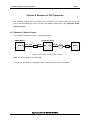
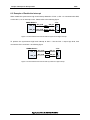
The hardware connection of GIO 1 is as following figure.
EMMA Mobile1
GIO_P1
TC74VCX16245FT
GIO_P1E
R669
MONI_1
1B2
1A2
LED_D1
LED5
R604
Figure 6-1 Hardware Connection of GIO 1 Output
Note: TC74VCX16245FT is a level shifter.
According to above figure, if change the GIO 1 output value, the LED 5 can sparkle.
Application Note S19897EJ1V0AN00
GND
Chapter 6 Example of GIO Operation
36/84
6.1.1 Operation Flow
Start
Change port 1 to GIO
[ em1_gpio_alternate; ]
Set port 1 to output port
[ em1_gpio_set_config; ]
i=0; i<100?
No
Yes
Write high level
[ em1_gpio_write_port; ]
Write low level
[ em1_gpio_write_port; ]
[ i++; ]
End
Figure 6-2 Set the Output
About the GIO function, please refer to the “Appendix B GIO Driver Function”.
Application Note S19897EJ1V0AN00
Chapter 6 Example of GIO Operation
37/84
6.1.2 Operation Detail
(1). Change the port 1 to normal GIO.
struct st_GPIO_SETTING gpio_val;
// Change the port to normal GIO.
gpio_val.gpio_port = 1;
em1_gpio_alternate (gpio_val);
The em1_gpio_alternate () finishes the following functions for GIO 1:
Change the GIO 1 port to normal GIO port.
CHG_PINSEL_G00[1:0] = 0;
(2). Set the port 1 to output mode.
// Set the default output mode
gpio_val.gpio_mode = 1;
em1_gpio_set_config (gpio_val);
The em1_gpio_set_config () finishes the following functions for GIO 1:
Set the GPIO output mode.
GIO_E1_L[1] = 1;
Disable the input and pull up/down.
CHG_PULL_G00[2:0] = 3;
(3). Write high level and low level by turns. As a result, the LED 5 connected with the GIO 1 will
sparkle.
// Output high level from default output port.
gpio_val.gpio_data= 1;
em1_gpio_write_port (gpio_val);
// Output low level from default output port.
gpio_val.gpio_data= 0;
em1_gpio_write_port (gpio_val);
The em1_gpio_write_port () finishes the following functions for GIO 1:
If output is high, enable the output bit and set the output bit 1.
GIO_OL_L[17] = 1;
GIO_OL_L[1] = 1;
If output is low, enable the output bit and set the output bit 0.
GIO_OL_L[17] = 1;
GIO_OL_L[1] = 0;
Application Note S19897EJ1V0AN00
Chapter 6 Example of GIO Operation
38/84
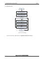
6.2 Example of Set the Input
The hardware connection of GIO 1 and GIO 7 is as following figure. GIO 1 and GIO 7 are connected
by jumper 17.
EMMA Mobile1
GIO_P1
GIO_P7
GIO_P1E
GIO_P7E
JP17
R95
R112
GIO_P1
GIO_P7
Figure 6-3 Hardware Connection of GIO 1 and GIO 7
According to above figure, if change the GIO 1 output value, the GIO 7 can read the value of GIO 1.
Application Note S19897EJ1V0AN00
Chapter 6 Example of GIO Operation
39/84
6.2.1 Operation Flow
Start
Yes
Change port 1 to GIO
[ em1_gpio_alternate; ]
The input is low?
Print right msg
No
Print error msg
Set port 1 to output port
[ em1_gpio_set_config; ]
Write high level to port 1
[ em1_gpio_write_port; ]
Change port 7 to GIO
[ em1_gpio_alternate; ]
Read data from port 7
[ em1_gpio_read_port; ]
Set port 7 to input port
[ em1_gpio_set_config; ]
Yes
Write low level to port 1
[ em1_gpio_write_port; ]
The input is high?
Print right msg
Print error msg
Read data from port 7
[ em1_gpio_read_port; ]
No
End
Figure 6-4 Set the Input
About the GIO function, please refer to the “Appendix B GIO Driver Function”.
Application Note S19897EJ1V0AN00
Chapter 6 Example of GIO Operation
6.2.2 Operation Detail
(1). Change the port 1 to normal GIO. Set the port 1 to output mode.
struct st_GPIO_SETTING gpio_output_val;
// Change the port to normal GIO
gpio_output_val.gpio_port = 1;
em1_gpio_alternate (gpio_output_val);
// Set the default output mode
gpio_output_val.gpio_mode = 1;
em1_gpio_set_config (gpio_output_val);
The em1_gpio_alternate () finishes the following functions for GIO 1:
Change the GIO 1 port to normal GIO port.
CHG_PINSEL_G00[1:0] = 0;
The em1_gpio_set_config () finishes the following functions for GIO 1:
Set the GPIO output mode.
GIO_E1_L[1] = 1;
Disable the input and pull up/down.
CHG_PULL_G00[2:0] = 3;
(2). Change the port 7 to normal GIO. Set the port 7 to input mode.
struct st_GPIO_SETTING gpio_input_val;
// Change the port to normal GIO
gpio_input_val.gpio_port = 7;
ret = em1_gpio_alternate (gpio_input_val);
// Set the default input mode
gpio_input_val.gpio_mode = 0;
ret = em1_gpio_set_config (gpio_input_val);
The em1_gpio_alternate () finishes the following functions for GIO 7:
Change the GIO 7 port to normal GIO port.
CHG_PINSEL_G00[15:14] = 0;
The em1_gpio_set_config () finishes the following functions for GIO 7:
Set the GPIO input mode.
GIO_E0_L[7] = 1;
Enable the input and disable pull up/down.
CHG_PULL_G00[30:28] = 7;
Application Note S19897EJ1V0AN00
40/84
Chapter 6 Example of GIO Operation
(3). Write low level from 1 port and read it from port 7.
// Output low level.
gpio_output_val.gpio_data = 0;
em1_gpio_write_port (gpio_output_val);
// Input
em1_gpio_read_port (&gpio_input_val);
The em1_gpio_write_port () finishes the following functions for GIO 1:
Enable the output bit and set the output bit 0.
GIO_OL_L[17] = 1;
GIO_OL_L[1] = 0;
The em1_gpio_read_port () finishes the following functions for GIO 7:
Read the input value.
data = GIO_I_L[7];
(4). Write high level from 1 port and read it from port 7.
// Output high level.
gpio_output_val.gpio_data = 1;
em1_gpio_write_port (gpio_output_val);
// Input
em1_gpio_read_port (&gpio_input_val);
The em1_gpio_write_port () finishes the following functions for GIO 1:
Enable the output bit and set the output bit 1.
GIO_OL_L[17] = 1;
GIO_OL_L[1] = 1;
The em1_gpio_read_port () finishes the following functions for GIO 7:
Read the input value.
data = GIO_I_L[7];
Application Note S19897EJ1V0AN00
41/84
Chapter 6 Example of GIO Operation
42/84
6.3 Example of Enable the Interrupt
When enable the synchronous high level interrupt detection of GIO 7, GIO 7 is connected with GND,
not the GIO 1, so no interrupt occurs. Please refer to the following figure.
EMMA Mobile1
GIO_P1
GIO_P7
JP17
GIO_P1E
GIO_P7E
R95
R112
GIO_P1
GIO_P7
GND
Figure 6-5 The Hardware Connnection without Synchronous High Interrupt
To produce the synchronous high level interrupt at GIO 7. Set the GIO 1 output high level, then
connect the GIO 1 and GIO 7 as following figure.
EMMA Mobile1
GIO_P1
GIO_P7
JP17
GIO_P1E
GIO_P7E
R95
R112
GIO_P1
GIO_P7
Figure 6-6 The Hardware Connnection with Synchronous High Interrupt
Application Note S19897EJ1V0AN00
Chapter 6 Example of GIO Operation
43/84
6.3.1 Operation Flow
Start
Change port 7 to GIO
[ em1_gpio_alternate; ]
Set port 7 to input port
[ em1_gpio_set_config; ]
Enable port 7 synchronous
high interrupt
[ em1_gpio_enable_int; ]
Wait interrupt from port 7
Yes
The interrupt occurs?
No
Change port 1 to GIO
[ em1_gpio_alternate; ]
Set port 1 to output port
[ em1_gpio_set_config; ]
Write high level to port 1
[ em1_gpio_write_port; ]
Wait interrupt from port 7
The interrupt occurs?
No
Disable port 7 interrupt;
[ em1_gpio_disable_int; ]
Yes
End
Figure 6-7 Enable the Interrupt
About the GIO function, please refer to the “Appendix B GIO Driver Function”.
Application Note S19897EJ1V0AN00
Chapter 6 Example of GIO Operation
44/84
6.3.2 Operation Detail
(1). Connect the GIO 7 to GND as figure 6-5.
(2). Change the port 7 to normal GIO. Set the port 7 to input mode.
struct st_GPIO_SETTING gpio_int_val;
// Set the input mode
gpio_int_val.gpio_port = 7;
em1_gpio_alternate (gpio_int_val);
gpio_int_val.gpio_mode = 0;
em1_gpio_set_config (gpio_int_val);
About the registers, please refer to the “Chapter 6.2.2 Operation Detail” of this document.
(3). Enable port 7 interrupt and wait the interrupt.
// Set the interrupt mode
gpio_int_val.gpio_int_mode = 0x2;
em1_gpio_enable_int (gpio_int_val);
The em1_gpio_enable_int () finishes the following functions for GIO 7:
Enable input and pull down the port.
CHG_PULL_G00[30:28] = 4;
Set the interrupt mode synchronous high level detection (0x2).
GIO_IDT0_L[31:28] = 2;
Clear the interrupt source.
GIO_IIR_L[7] = 1;
Enable the port interrupt.
GIO_IIA_L[7] = 1;
Send the GIO_INT_FIQ signal.
GIO_GSW_L[7] = 1;
Cancel the interrupt mask.
GIO_IEN_L[7] = 1;
Mount the interrupt handler.
irq_hook[50] = interrupt_handler;
Enable the GIO global interrupt.
SEC_IT0_IENS1[18] = 1;
Application Note S19897EJ1V0AN00
Chapter 6 Example of GIO Operation
45/84
INTC_IT0_IEN1[18] = 1;
Check the GIO global interrupt.
If INTC_IT0_IEN1[18] is 1, interrupt enable right.
(4). If there is an interrupt, the function executes successfully. If there is no interrupt, Change the
port 1 to normal GIO. Set the port 1 to output mode. Write high level to port 1.
struct st_GPIO_SETTING gpio_output_val;
// Set the default output mode
gpio_output_val.gpio_port = 1;
em1_gpio_alternate (gpio_output_val);
gpio_output_val.gpio_mode = 1;
em1_gpio_set_config (gpio_output_val);
// Output high level from default output port.
gpio_output_val.gpio_data= 1;
em1_gpio_write_port (gpio_output_val);
About the registers, please refer to the “Chapter 6.2.2 Operation Detail” of this document.
(5). In the second waiting the interrupt (the red process), connect the GIO 7 to GIO 1 as figure 6-6.
(6). An interrupt occurs at port 7.
Disable the port local interrupt and clear the interrupt source.
Application Note S19897EJ1V0AN00
Appendix A ASMU Driver Function
46/84
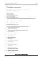
Appendix A ASMU Driver Function
A.1 ASMU Driver Function List
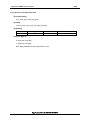
The following table shows the ASMU driver interface functions:
Table A-1 ASMU Driver Function List
Class
Driver
Function
Function Name
Function Detail
em1_asmu_set_reset
Set the reset state.
em1_asmu_get_reset
Get the reset state.
em1_asmu_set_clock_gate
em1_asmu_get_clock_gate
em1_asmu_set_clock_auto_gate
em1_asmu_get_clock_auto_gate
em1_asmu_set_dev_div
em1_asmu_get_dev_div
em1_asmu_change_div_freq_fmt
Enable/disable the clock gate.
Get the clock gate state.
Enable/disable the automatic clock gate.
Get the automatic clock gate state.
Set the divisor parameter.
Get the divisor parameter.
Change the divisor parameter to registre value.
Application Note S19897EJ1V0AN00
Appendix A ASMU Driver Function
47/84
A.2 ASMU Driver Function Detail
A.2.1 Set the Reset State
[Function Name]
em1_asmu_set_reset
[Format]
DRV_RESULT em1_asmu_set_reset (uint dev, uint state);
[Argument]
Parameter
Type
I/O
Detail
dev
uint
I
Device number
state
uint
I
Reset or reset release
[Function Return]
DRV_OK: The function executes successfully.
DRV_ERR_PARAM: The input parameter is error.
Application Note S19897EJ1V0AN00
Appendix A ASMU Driver Function
48/84
[Flow Chart]
Start
Get device register
[ register = dev & 0xFFFF0000; ]
Get device bit
[ bit = 0x1 << (dev & 0xFFFF); ]
register == ASMU_RESETCTRL0?
Yes
Enable or disable the device reset
[ ASMU_RESETCTRL0[bit] = 0/1; ]
No
register == ASMU_RESETREQ0?
Yes
No
register == ASMU_RESETREQ1?
Yes
Enable write reset control bit
[ ASMU_RESETREQxENA[bit] = 1; ]
Enable or disable device reset
[ ASMU_RESETREQx[bit] = 0/1; ]
No
register == ASMU_RESETREQ2?
Yes
Disable write reset control bit
[ ASMU_RESETREQxENA[bit] = 0; ]
No
register == ASMU_RESETREQ3?
Yes
No
register ==
ASMU_DTV_SAFE_RESET?
Yes
No
register ==
ASMU_USB_SAFE_RESET?
Yes
Enable or disable device reset
[ ASMU_DTV_SAFE_RESET[bit] = 0/1; ]
Enable or disable device reset
[ ASMU_USB_SAFE_RESET[bit] = 0/1; ]
No
End
Figure A-1 Set the Reset State
Note: x is 0, 1, 2 or 3.
Application Note S19897EJ1V0AN00
Appendix A ASMU Driver Function
49/84
[Note]
(1). According to the device number, find the device register and the device bit.
(2). If the device register is not in the ASMU_RESETCTRL0, ASMU_RESETREQx (x is 0, 1, 2
or 3), ASMU_DTV_SAFE_RESET and ASMU_USB_SAFE_RESET, the input parameter is
error.
(3). If the device register is in the ASMU_RESETCTRL0, ASMU_DTV_SAFE_RESET and
ASMU_USB_SAFE_RESET, set or clear the device bit.
If the device register is in the ASMU_RESETREQ0, ASMU_RESETREQ1,
ASMU_RESETREQ2 or ASMU_RESETREQ3:
// Enable write the reset bit.
ASMU_RESETREQxENA[bit] = 1;
// Set the reset bit state. 0: reset ; 1: reset release;
ASMU_RESETREQx[bit] = 0 / 1;
// Disable write the reset bit.
ASMU_RESETREQxENA[bit] = 0;
Application Note S19897EJ1V0AN00
Appendix A ASMU Driver Function
50/84
A.2.2 Get the Reset State
[Function Name]
em1_asmu_get_reset
[Format]
int em1_asmu_get_reset (uint dev);
[Argument]
Parameter
Type
I/O
Detail
dev
uint
I
Device number
[Function Return]
0: Reset release state.
1: Reset state.
DRV_ERR_PARAM: The input parameter is error.
Application Note S19897EJ1V0AN00
Appendix A ASMU Driver Function
51/84
[Flow Chart]
Start
Get device register
[ register = dev & 0xFFFF0000; ]
Get device bit
[ bit = 0x1 << (dev & 0xFFFF); ]
register == ASMU_RESETCTRL0?
Yes
Get device reset state
[ state = ASMU_RESETCTRL0[bit]; ]
No
register == ASMU_RESETREQ0?
Yes
Get device reset state
[ state = ASMU_RESETREQ0[bit]; ]
No
register == ASMU_RESETREQ1?
Yes
Get device reset state
[ state = ASMU_RESETREQ1[bit]; ]
No
register == ASMU_RESETREQ2?
Yes
Get device reset state
[ state = ASMU_RESETREQ2[bit]; ]
No
register == ASMU_RESETREQ3?
No
register ==
ASMU_DTV_SAFE_RESET?
No
register ==
ASMU_USB_SAFE_RESET?
No
Yes
Get device reset state
[ state = ASMU_RESETREQ3[bit]; ]
Yes
Get device reset state
[ state = ASMU_DTV_SAFE_RESET[bit]; ]
Yes
Get device reset state
[ state = ASMU_USB_SAFE_RESET[bit]; ]
End
Figure A-2 Get the Reset State
[Note]
(1). According to the device number, find the device register and the device bit.
(2). If the device register is not in the ASMU_RESETCTRL0, ASMU_RESETREQx (x is 0, 1, 2
or 3), ASMU_DTV_SAFE_RESET and ASMU_USB_SAFE_RESET, the input parameter is
error.
(3). Get the reset state according to the bit value in the device register.
Application Note S19897EJ1V0AN00
Appendix A ASMU Driver Function
52/84
A.2.3 Set the Clock Gate
[Function Name]
em1_asmu_set_clock_gate
[Format]
DRV_RESULT em1_asmu_set_clock_gate (uint dev, uint state);
[Argument]
Parameter
Type
I/O
Detail
dev
uint
I
Device number
state
uint
I
Open or close
[Function Return]
DRV_OK: The function executes successfully.
DRV_ERR_PARAM: The input parameter is error.
[Flow Chart]
Start
Get device register
[ register = dev & 0xFFFF0000; ]
Get device bit
[ bit = 0x1 << (dev & 0xFFFF); ]
register == ASMU_GCLKCTRL0?
Yes
No
Enable write device clock control bit
register == ASMU_GCLKCTRL1?
Yes
[ ASMU_GCLKCTRLxENA[bit] = 1; ]
Enable or disable device clock
[ ASMU_GCLKCTRLx[bit] = 0/1; ]
No
register == ASMU_GCLKCTRL2?
Yes
Disable write device clock control bit
[ ASMU_GCLKCTRLxENA[bit] = 0; ]
No
register == ASMU_GCLKCTRL3?
Yes
No
End
Figure A-3 Set the Clock Gate
Note: x is 0, 1, 2 or 3.
Application Note S19897EJ1V0AN00
Appendix A ASMU Driver Function
[Note]
(1). According to the device number, find the device register and the device bit.
(2). If the device register is not in the ASMU_GCLKCTRLx (x is 0, 1, 2 or 3), the input
parameter is error.
(3). If the device register is in the ASMU_GCLKCTRL0, ASMU_GCLKCTRL1,
ASMU_GCLKCTRL2 or ASMU_GCLKCTRL3:
// Enable write the clock gate control bit.
ASMU_GCLKCTRLxENA [bit] = 1;
// Set the clock gate state. 0: close; 1: open;
ASMU_GCLKCTRLx[bit] = 0 / 1;
// Disable write the clock gate control bit.
ASMU_GCLKCTRLxENAbit] = 0;
Application Note S19897EJ1V0AN00
53/84
Appendix A ASMU Driver Function
54/84
A.2.4 Get the Clock Gate
[Function Name]
em1_asmu_get_clock_gate
[Format]
int em1_asmu_get_clock_gate (uint dev);
[Argument]
Parameter
Type
I/O
Detail
dev
uint
I
Device number
[Function Return]
0: Close the clock gate.
1: Open the clock gate.
DRV_ERR_PARAM: The input parameter is error.
[Flow Chart]
Start
Get device register
[ register = dev & 0xFFFF0000; ]
Get device bit
[ bit = 0x1 << (dev & 0xFFFF); ]
register == ASMU_GCLKCTRL0?
Yes
Get device clock state
[ state = ASMU_GCLKCTRL0[bit]; ]
No
register == ASMU_GCLKCTRL1?
Yes
Get device clock state
[ state = ASMU_GCLKCTRL1[bit]; ]
No
register == ASMU_GCLKCTRL2?
Yes
Get device clock state
[ state = ASMU_GCLKCTRL2[bit]; ]
No
register == ASMU_GCLKCTRL3?
Yes
Get device clock state
[ state = ASMU_GCLKCTRL3[bit]; ]
No
End
Figure A-4 Get the Clock Gate
Application Note S19897EJ1V0AN00
Appendix A ASMU Driver Function
[Note]
(1). According to the device number, find the device register and the device bit.
(2). If the device register is not in the ASMU_GCLKCTRLx (x is 0, 1, 2 or 3), the input
parameter is error.
(3). Get the clock state according to the bit value.
Application Note S19897EJ1V0AN00
55/84
Appendix A ASMU Driver Function
56/84
A.2.5 Set the Clock Automatic Gate
[Function Name]
em1_asmu_set_clock_auto_gate
[Format]
DRV_RESULT em1_asmu_set_clock_auto_gate (uint dev, uint state);
[Argument]
Parameter
Type
I/O
Detail
dev
uint
I
Device number
state
uint
I
Open or close
[Function Return]
DRV_OK: The function executes successfully.
DRV_ERR_PARAM: The input parameter is error.
Application Note S19897EJ1V0AN00
Appendix A ASMU Driver Function
57/84
[Flow Chart]
Start
Get device register
[ register = dev & 0xFFFF0000; ]
Get device bit
[ bit = 0x1 << (dev & 0xFFFF); ]
register ==
ASMU_AHBCLKCTRL0?
Yes
Enable or disable device automatic clock
[ ASMU_AHBCLKCTRL0[bit] = 0/1; ]
No
register ==
ASMU_AHBCLKCTRL1?
Yes
No
register ==
ASMU_APBCLKCTRL0?
Yes
No
register ==
ASMU_APBCLKCTRL1?
Yes
Enable or disable device automatic clock
[ ASMU_AHBCLKCTRL1[bit] = 0/1; ]
Enable or disable device automatic clock
[ ASMU_APBCLKCTRL0[bit] = 0/1; ]
Enable or disable device automatic clock
[ ASMU_APBCLKCTRL1[bit] = 0/1; ]
No
register == ASMU_CLKCTRL?
Yes
Enable or disable device automatic clock
[ ASMU_CLKCTRL[bit] = 0/1; ]
No
End
Figure A-5 Set the Clock Automatic Gate
[Note]
(1). According to the device number, find the device register and the device bit.
(2). If the device register is not in the ASMU_AHBCLKCTRL0, ASMU_AHBCLKCTRL1,
ASMU_APBCLKCTRL0, ASMU_APBCLKCTRL1 or ASMU_CLKCTRL, the input parameter
is error.
(3). If the device register is in the ASMU_AHBCLKCTRL0, ASMU_AHBCLKCTRL1,
ASMU_APBCLKCTRL0, ASMU_APBCLKCTRL1 or ASMU_CLKCTRL, set or clear the
device bit.
Application Note S19897EJ1V0AN00
Appendix A ASMU Driver Function
58/84
A.2.6 Get the Clock Automatic Gate
[Function Name]
em1_asmu_get_clock_auto_gate
[Format]
int em1_asmu_get_clock_auto_gate (uint dev);
[Argument]
Parameter
Type
I/O
Detail
dev
uint
I
Device number
[Function Return]
0: Close the clock gate.
1: Open the clock gate.
DRV_ERR_PARAM: The input parameter is error.
Application Note S19897EJ1V0AN00
Appendix A ASMU Driver Function
59/84
[Flow Chart]
End
Get device register
[ register = dev & 0xFFFF0000; ]
Get device bit
[ bit = 0x1 << (dev & 0xFFFF); ]
register ==
ASMU_AHBCLKCTRL0?
Yes
Get device automatic clock state
[ state = ASMU_AHBCLKCTRL0[bit]; ]
No
register ==
ASMU_AHBCLKCTRL1?
Yes
No
register ==
ASMU_APBCLKCTRL0?
Yes
No
register ==
ASMU_APBCLKCTRL1?
Yes
Get device automatic clock state
[ state = ASMU_AHBCLKCTRL1[bit]; ]
Get device automatic clock state
[ state = ASMU_APBCLKCTRL0[bit]; ]
Get device automatic clock state
[ state = ASMU_APBCLKCTRL1[bit]; ]
No
register == ASMU_CLKCTRL?
Yes
Get device automatic clock state
[ state = ASMU_CLKCTRL[bit]; ]
No
End
Figure A-6 Get the Clock Automatic Gate
[Note]
(1). According to the device number, find the device register and the device bit.
(2). If the device register is not in the ASMU_AHBCLKCTRL0, ASMU_AHBCLKCTRL1,
ASMU_APBCLKCTRL0, ASMU_APBCLKCTRL1 or ASMU_CLKCTRL, the input parameter
is error.
(3). Get the clock automatic state according to the bit value.
Application Note S19897EJ1V0AN00
Appendix A ASMU Driver Function
60/84
A.2.7 Set the Peripheral Device Divisor
[Function Name]
em1_asmu_set_dev_div
[Format]
DRV_RESULT em1_asmu_set_dev_div (uint dev, uint div, uint num);
[Argument]
Parameter
Type
I/O
Detail
dev
uint
I
Device number
div
uint
I
Divisor parameter
num
uint
I
Device sub-number
[Function Return]
DRV_OK: The function executes successfully.
DRV_ERR_PARAM: The input parameter is error.
Application Note S19897EJ1V0AN00
Appendix A ASMU Driver Function
61/84
[Flow Chart]
Start
The device is ASMU_IICSCLK or
ASMU_PWMPWCLK?
Yes
num == 1?
No
num == 2?
Yes
No
The device is ASMU_MSPSCLK,
Or ASMU_SP0SCLK,
Or ASMU_SP1SCLK,
Or ASMU_SP2SCLK,
Or ASMU_MEMCRCLK,
Or ASMU_LCDLCLK,
Or ASMU_TIMTIN,
Or ASMU_MWISCLK,
Or ASMU_DMATCLK,
Or ASMU_U70SCLK,
Or ASMU_U71SCLK,
Or ASMU_U72SCLK,
Or ASMU_PM0SCLK,
Or ASMU_PM1SCLK.
Yes
Set divisor
Set divisor
[ dev[7:0] = div; ]
[ dev[23:16] = div; ]
No
End
Yes
Set divisor
[ dev = div; ]
Figure A-7 Set the Device Divisor
[Note]
(1). If the device is ASMU_IICSCLK or ASMU_PWMPWCLK.
If the device sub-number is 1, set the device divisor parameter to bit[7:0] of device divisor
register.
If the device sub-number is 2, set the device divisor parameter to bit[23:16] of device divisor
register.
(2). If the device is ASMU_MSPSCLK, ASMU_SP0SCLK, ASMU_SP1SCLK,
ASMU_SP2SCLK, ASMU_MEMCRCLK, ASMU_LCDLCLK, ASMU_TIMTIN,
ASMU_MWISCLK, ASMU_DMATCLK, ASMU_U70SCLK, ASMU_U71SCLK,
ASMU_U72SCLK, ASMU_PM0SCLK, ASMU_PM1SCLK, set the device divisor parameter.
Application Note S19897EJ1V0AN00
No
Appendix A ASMU Driver Function
62/84
A.2.8 Get the Peripheral Device Divisor
[Function Name]
em1_asmu_get_dev_div
[Format]
int em1_asmu_get_dev_div (uint dev, uint num);
[Argument]
Parameter
Type
I/O
Detail
dev
uint
I
Device number
num
uint
I
Device sub-number
[Function Return]
DRV_ERR_PARAM: The input parameter is error.
Other: The device dividing frequency parameter.
Application Note S19897EJ1V0AN00
Appendix A ASMU Driver Function
63/84
[Flow Chart]
Start
Get divisor
The device is ASMU_IICSCLK or
ASMU_PWMPWCLK?
Yes
num == 1?
No
num == 2?
Yes
No
The device is ASMU_MSPSCLK,
Or ASMU_SP0SCLK,
Or ASMU_SP1SCLK,
Or ASMU_SP2SCLK,
Or ASMU_MEMCRCLK,
Or ASMU_LCDLCLK,
Or ASMU_TIMTIN,
Or ASMU_MWISCLK,
Or ASMU_DMATCLK,
Or ASMU_U70SCLK,
Or ASMU_U71SCLK,
Or ASMU_U72SCLK,
Or ASMU_PM0SCLK,
Or ASMU_PM1SCLK.
Yes
Get divisor
Get divisor
[ div = dev_div[7:0]; ]
[ div = dev_div[23:16]; ]
No
End
Yes
Get divisor
[ div = dev_div; ]
Figure A-8 Get the Device Divisor
[Note]
(1). Get the device divisor (div).
(2). If the device is ASMU_IICSCLK or ASMU_PWMPWCLK.
If the device sub-number is 1, get the device divisor parameter by div[7:0].
If the device sub-number is 2, get the device divisor parameter by div[23:16].
(3). If the device is ASMU_MSPSCLK, ASMU_SP0SCLK, ASMU_SP1SCLK,
ASMU_SP2SCLK, ASMU_MEMCRCLK, ASMU_LCDLCLK, ASMU_TIMTIN,
ASMU_MWISCLK, ASMU_DMATCLK, ASMU_U70SCLK, ASMU_U71SCLK,
ASMU_U72SCLK, ASMU_PM0SCLK, ASMU_PM1SCLK, get the device divisor parameter by
div.
Application Note S19897EJ1V0AN00
No
Appendix A ASMU Driver Function
64/84
A.2.9 Change the Divisor Parameter to Register Value
[Function Name]
em1_asmu_change_div_freq_fmt
[Format]
int em1_asmu_change_div_freq_fmt (uint div);
[Argument]
Parameter
Type
I/O
Detail
div
uint
I
Divisor parameter
[Function Return]
DRV_ERR_PARAM: The input parameter is error.
Other: The dividing frequency register value.
[Flow Chart]
None.
[Note]
None.
Application Note S19897EJ1V0AN00
Appendix B GIO Driver Function
65/84
Appendix B GIO Driver Function
B.1 GIO Driver Function List
The following table shows the GIO driver interface functions:
Table B-1 GIO Driver Function List
Class
Driver
Function
Function Name
Function Detail
em1_gpio_init
Initialize the GIO.
em1_gpio_alternate
Change the port to GIO.
em1_gpio_set_config
em1_gpio_get_config
em1_gpio_write_port
em1_gpio_read_port
em1_gpio_enable_int
em1_gpio_disable_int
_em1_gpio_int_0_31
_em1_gpio_int_32_63
_em1_gpio_int_64_95
_em1_gpio_int_96_117
_em1_gpio_set_output_fmt
_em1_gpio_set_int_mode_fmt
Set the port output mode or input mode.
Get the port output mode or input mode.
Write data to port.
Read data from port.
Enable port interrupt.
Disable port interrupt.
Port 0-31 interrupt handler.
Port 32-63 interrupt handler.
Port 64-95 interrupt handler.
Port 96-127 interrupt handler.
Set the output data format.
Set the interrupt mode format.
Application Note S19897EJ1V0AN00
Appendix B GIO Driver Function
66/84
B.2 GIO Global Variable Define
The following table shows the GIO global variable define:
Table B-2 Global Variable Define
Name
Type
Detail
g_gpio_int
volatile uchar
GIO interrupt or not.
Application Note S19897EJ1V0AN00
Appendix B GIO Driver Function
67/84
B.3 GIO Structure Define
The following table shows the GIO structure define:
Table B-3 Structure Define
Structure Name
Detail
struct st_GPIO_SETTING
GIO setting information.
B.3.1 st_GPIO_SETTING
Table B-4 Structure of st_GPIO_SETTING
Member
Type
Detail
gpio_port
uchar
The port number.
gpio_mode
gpio_data
gpio_int_mode
uchar
uchar
uchar
Input mode or Output mode.
Input data or output data.
The interrupt mode.
Application Note S19897EJ1V0AN00
Appendix B GIO Driver Function
B.4 GIO Driver Function Detail
B.4.1 Initialize the GIO
[Function Name]
em1_gpio_init
[Format]
DRV_RESULT em1_gpio_init (void);
[Argument]
None.
[Function Return]
DRV_OK: The function executes successfully.
DRV_ERR_PARAM: The input parameter is error.
Application Note S19897EJ1V0AN00
68/84
Appendix B GIO Driver Function
69/84
[Flow Chart]
Start
Reset GIO
[ ASMU_RESETREQ0ENA[26] = 1;
ASMU_RESETREQ0[26] = 0;
ASMU_RESETREQ0ENA[26] = 1; ]
Reset release GIO
[ ASMU_RESETREQ0ENA[26] = 1;
ASMU_RESETREQ0[26] = 1;
ASMU_RESETREQ0ENA[26] = 1; ]
Disable GIO global interrupt
[ SEC_IT0_IDSS1[18] = 1;
INTC_IT0_IDS1[18] = 1;
SEC_IT0_IDSS1[19] = 1;
INTC_IT0_IDS1[19] = 1;
SEC_IT0_IDSS1[20] = 1;
INTC_IT0_IDS1[20] = 1;
SEC_IT0_IDSS1[21] = 1;
INTC_IT0_IDS1[21] = 1;
SEC_IT0_IDSS2[15] = 1;
INTC_IT0_IDS2[15] = 1;
SEC_IT0_IDSS2[16] = 1;
INTC_IT0_IDS2[16] = 1;
SEC_IT0_IDSS0[26] = 1;
INTC_IT0_IDS0[26] = 1;
SEC_IT0_IDSS0[27] = 1;
INTC_IT0_IDS0[27] = 1; ]
End
Figure B-1 GIO Initialize
[Note]
(1). Reset on the GIO module, then reset off the GIO module.
(2). Disable the all GIO global interrupt.
Application Note S19897EJ1V0AN00
Appendix B GIO Driver Function
70/84
B.4.2 Alternate the Port
[Function Name]
em1_gpio_alternate
[Format]
DRV_RESULT em1_gpio_alternate (struct st_GPIO_SETTING gpio_value);
[Argument]
Parameter
Type
I/O
Detail
gpio_value
struct st_GPIO_SETTING
I
GIO information
[Function Return]
DRV_OK: The function executes successfully.
DRV_ERR_PARAM: The input parameter is error.
[Flow Chart]
Start
port >= 118 ?
Yes
No
Switch port to GIO
[ bit = 0x1 << ( ( port % 16 ) * 2 );
CHG_PINSEL_Gxxx[bit<<1:bit] = 0;
End
Figure B-2 GIO Alternate
Note: x is 00, 16, 32, 48, 64, 80, 96 or 112.
[Note]
(1). Check the GIO number valid.
The EMMA Mobile1 has only 118 GIO.
(2). Switch the port to GIO.
There are two bits to control the port alternate function. If the two bits are 0, the port changes
to normal GIO.
Application Note S19897EJ1V0AN00
Appendix B GIO Driver Function
71/84
B.4.3 Set the Port Configure
[Function Name]
em1_gpio_set_config
[Format]
DRV_RESULT em1_gpio_set_config (struct st_GPIO_SETTING gpio_value);
[Argument]
Parameter
Type
I/O
Detail
gpio_value
struct st_GPIO_SETTING
I
GIO information
[Function Return]
DRV_OK: The function executes successfully.
DRV_ERR_PARAM: The input parameter is error.
Application Note S19897EJ1V0AN00
Appendix B GIO Driver Function
72/84
[Flow Chart]
Start
Yes
port >= 118 ?
No
Yes
The mode is
output ?
No
Set output mode
Set input mode
[ bit = 0x1 << ( port % 32 );
GPIO_E1_xxx[bit] = 1; ]
[ bit = 0x1 << ( port % 32 );
GPIO_E0_xxx[bit] = 1; ]
Disable input and pull up/down
Enable input and disable pull
up/down
[ bit = 0x1 << ( ( port % 8 ) * 4);
CHG_PULL_yyy[bit] = 1;
CHG_PULL_yyy[bit<<1] = 1;
CHG_PULL_yyy[bit<<2] = 0; ]
[ bit = 0x1 << ( ( port % 8 ) * 4);
Addr_CHG_PULL[bit] = 1;
Addr_CHG_PULL[bit<<1] = 1;
Addr_CHG_PULL[bit<<2] = 1; ]
End
Figure B-3 Set the GIO Configure
Note: xxx is L, H, HH or HHH;
yyy is 00, 08, 16, 24, 32, 40, 48, 56, 64, 72, 80, 88, 96, 104, 112.
[Note]
(1). Check the GIO number valid.
The EMMA Mobile1 has only 118 GIO.
(2). If the mode is output, set the GIO_E1_xxx.
Disable the input and pull up/down by CHG_PULL_yyy.
(3). If the mode is input, set the GIO_E0_xxx.
Enable the input and disable pull up/down by CHG_PULL_yyy.
Application Note S19897EJ1V0AN00
Appendix B GIO Driver Function
73/84
B.4.4 Get the Port Configure
[Function Name]
em1_gpio_get_config
[Format]
DRV_RESULT em1_gpio_get_config (struct st_GPIO_SETTING *p_gpio_value);
[Argument]
Parameter
Type
I/O
Detail
p_gpio_value
struct st_GPIO_SETTING *
O
GIO information
[Function Return]
DRV_OK: The function executes successfully.
DRV_ERR_PARAM: The input parameter is error.
[Flow Chart]
Start
port >= 118 ?
Yes
No
Get mode of GIO
[ bit = 0x1 << ( port % 32 );
mode = GIO_EM_xxx[bit]; ]
End
Figure B-4 Get the GIO Configure
Note: xxx is L, H, HH or HHH.
[Note]
(1). Check the GIO number valid.
The EMMA Mobile1 has only 118 GIO.
(2). Get the input mode or output mode by the bit value in the GIO_EM_xxx register.
Application Note S19897EJ1V0AN00
Appendix B GIO Driver Function
74/84
B.4.5 Write Data to Port
[Function Name]
em1_gpio_write_port
[Format]
DRV_RESULT em1_gpio_write_port (struct st_GPIO_SETTING gpio_value);
[Argument]
Parameter
Type
I/O
Detail
gpio_value
struct st_GPIO_SETTING
I
GIO information
[Function Return]
DRV_OK: The function executes successfully.
DRV_ERR_PARAM: The input parameter is error.
[Flow Chart]
Start
Yes
port >= 118 ?
No
Output high?
Set output high
Set output low
[ bit = 0x1 << ( port % 16 );
data = ( bit << 16 ) | bit; ]
[ bit = 0x1 << ( port % 16 );
data = ( bit << 16 ); ]
Write data to port
[ GPIO_OL_xxx = data;
Or GPIO_OH_xxx = data; ]
End
Figure B-5 Write Data
Note: xxx is L, H, HH or HHH.
Application Note S19897EJ1V0AN00
Appendix B GIO Driver Function
[Note]
(1). Check the GIO number valid.
The EMMA Mobile1 has only 118 GIO.
(2). If output is high, enable the output bit and set the output bit 1.
If output is low, enable the output bit and set the output bit 0.
(3). Write the output value by GPIO_OL_xxx or GPIO_OH_xxx register.
Application Note S19897EJ1V0AN00
75/84
Appendix B GIO Driver Function
76/84
B.4.6 Read Data from Port
[Function Name]
em1_gpio_read_port
[Format]
DRV_RESULT em1_gpio_read_port (struct st_GPIO_SETTING *p_gpio_value);
[Argument]
Parameter
Type
I/O
Detail
p_gpio_value
struct st_GPIO_SETTING
O
GIO information
[Function Return]
DRV_OK: The function executes successfully.
DRV_ERR_PARAM: The input parameter is error.
[Flow Chart]
Start
port >= 118 ?
Yes
No
Read data from port
[ bit = 0x1 << ( port % 32 );
data = GIO_I_xxx[bit]; ]
End
Figure B-6 Read Data
Note: xxx is L, H, HH or HHH.
[Note]
(1). Check the GIO number valid.
The EMMA Mobile1 has only 118 GIO.
(2). Read the input value from the bit in the GIO_I_xxx register.
Application Note S19897EJ1V0AN00
Appendix B GIO Driver Function
77/84
B.4.7 Enable Port Interrupt
[Function Name]
em1_gpio_enable_int
[Format]
DRV_RESULT em1_gpio_enable_int (struct st_GPIO_SETTING gpio_value);
[Argument]
Parameter
Type
I/O
Detail
gpio_value
struct st_GPIO_SETTING
I
GIO information
[Function Return]
DRV_OK: The function executes successfully.
DRV_ERR_PARAM: The input parameter is error.
Application Note S19897EJ1V0AN00
Appendix B GIO Driver Function
78/84
[Flow Chart]
Please refer to the figure B-7 and B-8. B-8 shows the details about “Enable 0-31 interrupt”.
“Enable 32-63 interrupt”, “Enable 64-95 interrupt” and “Enable 96-118 interrupt” are similar to
“Enable 0-31 interrupt”.
Start
Yes
port >= 118 ?
No
Interrupt mode is in
synchronous high or low ?
No
Yes
Interrupt mode is
synchronous high?
Yes
No
Pull down and enable input
Pull up and enable input
[ bit = 0x1 << ( ( port % 8 ) * 4 );
CHG_PULL_xxx[bit] = 0;
CHG_PULL_xxx[bit<<1] = 0;
CHG_PULL_xxx[bit<<2] = 1; ]
[ bit = 0x1 << ( ( port % 8 ) * 4 );
CHG_PULL_xxx[bit] = 0;
CHG_PULL_xxx[bit<<1] = 1;
CHG_PULL_xxx[bit<<2] = 1; ]
port < 32 ?
Yes
Enable 0-31 interrupt
No
port < 64 ?
Yes
Enable 32-63 interrupt
No
port < 96 ?
Yes
Enable 64-95 interrupt
No
port < 118 ?
Yes
Enable 96-117 interrupt
No
End
Figure B-7 Enable the GIO Interrupt (1)
Note: xxx is 00, 08, 16, 24, 32, 40, 48, 56, 64, 72, 80, 88, 96, 104, 112.
Application Note S19897EJ1V0AN00
Appendix B GIO Driver Function
79/84
Start
Find port bit
[ bit = 0x1 << (port % 32); ]
Set interrupt mode
[ bit2 = (port % 8) * 4;
GIO_IDTx_L[bit2<<3:bit2] = 0x2/0x3; ]
Clear interrupt source
[ GIO_IIR_L[bit] = 1; ]
Enable port interrupt
[ GIO_IIA_L[bit] = 1;
Delay 3 interrupt clock; ]
Send GIO_INT_FIQ signal
[ GIO_GSW_L[bit] = 1; ]
Cancel interrupt mask
[ GIO_IEN_L[bit] = 1; ]
Yes
No
port < 16?
Mount interrupt handler
Mount interrupt handler
[ irq_hook[18] = interrupt_handler; ]
[ irq_hook[19] = interrupt_handler; ]
Enable port global interrupt
Enable port global interrupt
[ SEC_IT0_IENS1[18] = 1;
INTC_IT0_IEN1[18] = 1; ]
[ SEC_IT0_IENS1[19] = 1;
INTC_IT0_IEN1[19] = 1; ]
( INTC_IT0_IEN1 &
(1<<18) ) == 0?
( INTC_IT0_IEN1 &
(1<<19) ) == 0?
No
Yes
Yes
No
Clear port interrupt
[ GIO_IDS_L[18] = 1;
Or GIO_IDS_L[19] = 1; ]
End
Figure B-8 Enable the GIO Interrupt (2)
Note: x is 0, 1, 2 or 3.
[Note]
(1). Check the GIO number and the interrupt mode valid. The EMMA Mobile1 supports 10
interrupt mode detections:
Synchronous rising edge detection;
Synchronous falling edge detection;
Application Note S19897EJ1V0AN00
Appendix B GIO Driver Function
Synchronous high level detection;
Synchronous low level detection;
Synchronous both edge detection;
Asynchronous rising edge detection;
Asynchronous falling edge detection;
Asynchronous high level detection;
Asynchronous low level detection;
Asynchronous both edge detection;
80/84
In this function, only synchronous high level detection and synchronous low level detection are
supported.
(2). If the detection mode is high level detection, enable input and pull down the port.
If the detection mode is low level detection, enable input and pull up the port.
(3). set the interrupt mode by interrupt mode register GIO_IDTx_yyy.
Synchronous high level detection is 0x2.
Synchronous low level detection is 0x3.
(4). Clear the interrupt source, enable the port interrupt, send the GIO_INT_FIQ signal, cancel
the interrupt mask.
(5). Mount the interrupt handler and enable the GIO global interrupt.
Check the GIO global interrupt, if it is masked, clear the GIO local interrupt return error. If the
GIO global interrupt is enable, return ok.
Application Note S19897EJ1V0AN00
Appendix B GIO Driver Function
81/84
B.4.8 Disable Port Interrupt
[Function Name]
em1_gpio_disable_int
[Format]
DRV_RESULT em1_gpio_disable_int (struct st_GPIO_SETTING gpio_value);
[Argument]
Parameter
Type
I/O
Detail
gpio_value
struct st_GPIO_SETTING
I
GIO information
[Function Return]
DRV_OK: The function executes successfully.
DRV_ERR_PARAM: The input parameter is error.
[Flow Chart]
Start
port >= 118 ?
Yes
No
Disable local interrupt
[ bit = 0x1 << port;
GIO_IDS_L[bit] = 1;
Or GIO_IDS_H[bit] = 1;
Or GIO_IDS_HH[bit] = 1;
Or GIO_IDS_HHH[bit] = 1; ]
End
Figure B-9 Disable the GIO Interrupt
[Note]
(1). Check the GIO number valid.
The EMMA Mobile1 has only 118 GIO.
(2). Disable the GIO local interrupt.
Application Note S19897EJ1V0AN00
Appendix B GIO Driver Function
82/84
B.4.9 Interrupt Handler
[Function Name]
_em1_gpio_int_0_31
[Format]
void _em1_gpio_int_0_31 (void);
[Argument]
None.
[Function Return]
None.
[Flow Chart]
Start
Read the interrupt value;
[ int = GIO_MST_L; ]
Initialize the variable;
[ port = 0 ]
port < 32?
No
Yes
( int & 0x1 ) != 0?
No
Yes
Disable the interrupt;
[ bit = 0x1 << port;
GIO_IDS_L[bit] = 1; ]
Clear the interrupt source;
[ GIO_IIR_L[bit] = 1; ]
Move the interrupt bit left;
[ int = int >> 1;
port++; ]
End
Figure B-10 The Interrupt Handler of GIO 0 -31
Application Note S19897EJ1V0AN00
Appendix B GIO Driver Function
83/84
[Note]
(1). Read the interrupt source 0 – 31 by GIO_MST_L register.
(2). If the x (x is in the 0 - 31) bit is 1, x port occurs an interrupt.
(3). Disable the x port local interrupt and clear the interrupt source.
(4). _em1_gpio_int_32_63, _em1_gpio_int_64_95 and _em1_gpio_int_96_117 are similar to
the function _em1_gpio_int_0_31.
Application Note S19897EJ1V0AN00
ANNEX Modification History
84/84
ANNEX Modification History
Number
Ver 1.00
Modification Contents
Author
New version
Application Note S19897EJ1V0AN00
Date
Aug 4,2009