1
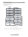
To our customers, Old Company Name in Catalogs and Other Documents On April 1st, 2010, NEC Electronics Corporation merged with Renesas Technology Corporation, and Renesas Electronics Corporation took over all the business of both companies. Therefore, although the old company name remains in this document, it is a valid Renesas Electronics document. We appreciate your understanding. Renesas Electronics website: http://www.renesas.com April 1st, 2010 Renesas Electronics Corporation Issued by: Renesas Electronics Corporation (http://www.renesas.com) Send any inquiries to http://www.renesas.com/inquiry. Notice 1. 2. 3. 4. 5. 6. 7. All information included in this document is current as of the date this document is issued. Such information, however, is subject to change without any prior notice. Before purchasing or using any Renesas Electronics products listed herein, please confirm the latest product information with a Renesas Electronics sales office. Also, please pay regular and careful attention to additional and different information to be disclosed by Renesas Electronics such as that disclosed through our website. Renesas Electronics does not assume any liability for infringement of patents, copyrights, or other intellectual property rights of third parties by or arising from the use of Renesas Electronics products or technical information described in this document. No license, express, implied or otherwise, is granted hereby under any patents, copyrights or other intellectual property rights of Renesas Electronics or others. You should not alter, modify, copy, or otherwise misappropriate any Renesas Electronics product, whether in whole or in part. Descriptions of circuits, software and other related information in this document are provided only to illustrate the operation of semiconductor products and application examples. You are fully responsible for the incorporation of these circuits, software, and information in the design of your equipment. Renesas Electronics assumes no responsibility for any losses incurred by you or third parties arising from the use of these circuits, software, or information. When exporting the products or technology described in this document, you should comply with the applicable export control laws and regulations and follow the procedures required by such laws and regulations. You should not use Renesas Electronics products or the technology described in this document for any purpose relating to military applications or use by the military, including but not limited to the development of weapons of mass destruction. Renesas Electronics products and technology may not be used for or incorporated into any products or systems whose manufacture, use, or sale is prohibited under any applicable domestic or foreign laws or regulations. Renesas Electronics has used reasonable care in preparing the information included in this document, but Renesas Electronics does not warrant that such information is error free. Renesas Electronics assumes no liability whatsoever for any damages incurred by you resulting from errors in or omissions from the information included herein. Renesas Electronics products are classified according to the following three quality grades: “Standard”, “High Quality”, and “Specific”. The recommended applications for each Renesas Electronics product depends on the product’s quality grade, as indicated below. You must check the quality grade of each Renesas Electronics product before using it in a particular application. You may not use any Renesas Electronics product for any application categorized as “Specific” without the prior written consent of Renesas Electronics. Further, you may not use any Renesas Electronics product for any application for which it is not intended without the prior written consent of Renesas Electronics. Renesas Electronics shall not be in any way liable for any damages or losses incurred by you or third parties arising from the use of any Renesas Electronics product for an application categorized as “Specific” or for which the product is not intended where you have failed to obtain the prior written consent of Renesas Electronics. The quality grade of each Renesas Electronics product is “Standard” unless otherwise expressly specified in a Renesas Electronics data sheets or data books, etc. “Standard”: 8. 9. 10. 11. 12. Computers; office equipment; communications equipment; test and measurement equipment; audio and visual equipment; home electronic appliances; machine tools; personal electronic equipment; and industrial robots. “High Quality”: Transportation equipment (automobiles, trains, ships, etc.); traffic control systems; anti-disaster systems; anticrime systems; safety equipment; and medical equipment not specifically designed for life support. “Specific”: Aircraft; aerospace equipment; submersible repeaters; nuclear reactor control systems; medical equipment or systems for life support (e.g. artificial life support devices or systems), surgical implantations, or healthcare intervention (e.g. excision, etc.), and any other applications or purposes that pose a direct threat to human life. You should use the Renesas Electronics products described in this document within the range specified by Renesas Electronics, especially with respect to the maximum rating, operating supply voltage range, movement power voltage range, heat radiation characteristics, installation and other product characteristics. Renesas Electronics shall have no liability for malfunctions or damages arising out of the use of Renesas Electronics products beyond such specified ranges. Although Renesas Electronics endeavors to improve the quality and reliability of its products, semiconductor products have specific characteristics such as the occurrence of failure at a certain rate and malfunctions under certain use conditions. Further, Renesas Electronics products are not subject to radiation resistance design. Please be sure to implement safety measures to guard them against the possibility of physical injury, and injury or damage caused by fire in the event of the failure of a Renesas Electronics product, such as safety design for hardware and software including but not limited to redundancy, fire control and malfunction prevention, appropriate treatment for aging degradation or any other appropriate measures. Because the evaluation of microcomputer software alone is very difficult, please evaluate the safety of the final products or system manufactured by you. Please contact a Renesas Electronics sales office for details as to environmental matters such as the environmental compatibility of each Renesas Electronics product. Please use Renesas Electronics products in compliance with all applicable laws and regulations that regulate the inclusion or use of controlled substances, including without limitation, the EU RoHS Directive. Renesas Electronics assumes no liability for damages or losses occurring as a result of your noncompliance with applicable laws and regulations. This document may not be reproduced or duplicated, in any form, in whole or in part, without prior written consent of Renesas Electronics. Please contact a Renesas Electronics sales office if you have any questions regarding the information contained in this document or Renesas Electronics products, or if you have any other inquiries. (Note 1) “Renesas Electronics” as used in this document means Renesas Electronics Corporation and also includes its majorityowned subsidiaries. (Note 2) “Renesas Electronics product(s)” means any product developed or manufactured by or for Renesas Electronics. Application Note Multimedia Processor for Mobile Applications Timer -------------------------------------------------------------------------------------- EMMA Mobile1 Document No. Date Published S19894EJ1V0AN00 Aug. 2009 2009 Printed in Japan PREFACE PREFACE Purpose The purpose of this document is to specify the usage of the Timer interface. Organization This document includes the following: Introduction Usage of Timer Interface Example of Timer Operation Timer Driver Function Notation Here explains the meaning of following words in text: Related document Note Explanation of item indicated in the text Caution Information to which user should afford special attention Remark Supplementary information The following tables list related documents. Reference Document Document Name Version/date Author S19265EJ1V0UM00_ASMUGIO.pdf 1st edition NECEL S19268EJ1V0UM00_1chip.pdf 1st edition NECEL 1 Chip User’s Manual S19266EJ1V0UM00_TIMER.pdf 1st edition NECEL Timer User’s Manual S19907EJ1V0AN00_GD.pdf 1st edition NECEL GD Spec Application Note S19894EJ1V0AN00 Description ASMU/GIO User’s Manual PREFACE Disclaimers The information contained in this document is subject to change without prior notice in the future. Refer to the latest applicable data sheet(s) and user’s manual when designing a product for mass production. No part of this document may be copied or reproduced in any form or by any means without the prior written consent of NEC Electronics. NEC Electronics assumes no responsibility for any errors that may appear in this document. NEC Electronics does not assume any liability for infringement of patents, copyrights or other intellectual property rights of third parties by or arising from the use of NEC Electronics products listed in this documents or any other liability arising from the use of such products. No license, express, implied or otherwise, is granted under any patents, copyrights or other intellectual property rights of NEC Electronics or others. Descriptions of circuits, software and other related information in this document are provided for illustrative purposes in semiconductor product operation and application examples. The incorporation of these circuits, software and information in the design of a customers’ equipment shall be done under the full responsibility of the customer. NEC Electronics assume no responsibility for any losses incurred by customers or third parties arising from the use of these circuits, software and information. While NEC Electronics endeavors to enhance the quality, reliability and safety of NEC Electronics products, customers agree and acknowledge that possibility of defects thereof cannot be eliminated entirely. To minimize risks of damage to property or injury (including death) to persons arising from defects in NEC Electronics products, customers must incorporate sufficient safety measures in their design, such as redundancy, firecontainment and anti-failure features. Note) 1. “NEC Electronics” as used in this document means NEC Electronics Corporation and also includes its majority-owned subsidiaries. 2. “NEC Electronics products” means any product developed or manufactured by or for NEC Electronics (as defined above) 3. All trademarks or registered trademarks are the property of their respective owners. Registered trademarks ® and trademarks™ are not noted in this document. Application Note S19894EJ1V0AN00 INDEX 4/34 CONTENTS Chapter 1 Introduction ...................................................................................................................... 6 1.1 Outline........................................................................................................................................ 6 1.2 Development Environment ........................................................................................................ 6 Chapter 2 Usage of Timer Interface ................................................................................................. 7 2.1 Timer Overview .......................................................................................................................... 7 2.2 Timer Details .............................................................................................................................. 8 Chapter 3 Example of Timer Operation .......................................................................................... 10 3.1 Example of General Operation .................................................................................................11 3.1.1 Operation Flow ...............................................................................................................11 3.1.2 Operation Detail............................................................................................................. 12 3.2 Example of Set Watchdog ....................................................................................................... 16 3.2.1 Operation Flow .............................................................................................................. 16 3.2.2 Operation Detail............................................................................................................. 17 Appendix A Timer Driver Function................................................................................................. 19 A.1 Timer Driver Function List ....................................................................................................... 19 A.2 Timer Driver Function Detail.................................................................................................... 20 A.2.1 Initialize Timer ............................................................................................................... 20 A.2.2 Start Timer ..................................................................................................................... 22 A.2.3 Stop Timer ..................................................................................................................... 24 A.2.4 Pause Timer .................................................................................................................. 26 A.2.5 Resume Timer............................................................................................................... 28 A.2.6 Get Timer Configure...................................................................................................... 30 A.2.7 Timer TI0 Interrupt Handler ........................................................................................... 32 ANNEX Modification History............................................................................................................ 34 Application Note S19894EJ1V0AN00 INDEX 5/34 LIST OF TABLES Table 1-1 Hardware Environment ....................................................................................... 6 Table 1-2 Software Environment......................................................................................... 6 Table 2-1 Calculation of Timer Count ................................................................................. 8 Table A-1 Timer Driver Function List ................................................................................ 19 LIST OF FIGURES Figure 2-1 Timer Operation Overview................................................................................. 7 Figure 3-1 Example of General Operation ........................................................................ 11 Figure 3-2 Example of Set Watchdog ............................................................................... 16 Figure A-1 Initialize Timer ................................................................................................. 21 Figure A-2 Start Timer....................................................................................................... 23 Figure A-3 Stop Timer ....................................................................................................... 25 Figure A-4 Pause Timer .................................................................................................... 27 Figure A-5 Resume Timer................................................................................................. 29 Figure A-6 Get Timer Configure........................................................................................ 31 Figure A-7 Timer TI0 Interrupt Handler ............................................................................. 33 Application Note S19894EJ1V0AN00 Chapter 1 Introduction 6/34 Chapter 1 Introduction 1.1 Outline This document introduces how to use the timer interface of EMMA Mobile1, including the following functions: How to set general operation of timer (start, pause, resume and stop). How to set watchdog. The timer module (ATIM) is a programmable timer counter that enables 32-bit counting (1 to 0xFFFFFFFF). About the details of functions please refer to “CHAPTER 1 OVERVIEW” of EMMA Mobile1 Timer user’s manual. 1.2 Development Environment Hardware environment of this project is listed as below. Table 1-1 Hardware Environment Name Version Maker EMMA Mobile1 evaluation board (PSKCH2YS-0016-01) - NEC Electronics M20 Kyoto Microcomputer Co. Ltd PARTNER-Jet ICE ARM Software used in this project is listed as below. Table 1-2 Software Environment Name Version Maker GNUARM Toolchain V4.3.2 GNU WJETSET-ARM V5.10a Kyoto Microcomputer Co. Ltd Application Note S19894EJ1V0AN00 Chapter 2 Usage of Timer Interface 7/34 Chapter 2 Usage of Timer Interface 2.1 Timer Overview Start Open clocks Reset release Set count clock Set count out value Enable interrupt Start timer Get timer configure Timer interrupt handler End Figure 2-1 Timer Operation Overview Application Note S19894EJ1V0AN00 Chapter 2 Usage of Timer Interface 8/34 2.2 Timer Details (1). Open clocks. The related registers are as follow: ASMU_GCLKCTRL3ENA; ASMU_GCLKCTRL3; (2). Reset release. The related registers are as follow: ASMU_RESETREQ1ENA; ASMU_RESETREQ1; (3). Set count clock. The related registers are as follow: ASMU_DIVTIMTIN; ASMU_TI0TIN_SEL; ASMU_TI1TIN_SEL; ASMU_TI2TIN_SEL; ASMU_TI3TIN_SEL; ASMU_TGnTIN_SEL; The Timers have 3 clock source, PLL3, 32K, 32.768K. And a wide range of counting is possible by using a combination of input frequency and timer count settings. The following table shows setting examples. The term [seconds] in this table refers to the interval at which the TOUT signal is asserted. Table 2-1 Calculation of Timer Count TIN (Input Frequency) Timer Count Setting Value 0000_0000H 0000_FFFFH FFFF_FFFFH 32.768 kHz 30.52 * 10E−6 [seconds] 2 [seconds] 131071.99 [seconds] 15.616 MHz 64.04 * 10E−9 [seconds] 4.20 * 10E−3 [seconds] 275.04 [seconds] Expression: (1/TIN) * (Count setting value + 1). Example: 1/32.768 kHz * (0000_FFFFH + 1) = 30.52 * 10E−6 * 65536 = 2 [seconds]. Application Note S19894EJ1V0AN00 Chapter 2 Usage of Timer Interface (4). Set count out value. The related registers are as follow: TIM_xxx_OP; TIM_xxx_CLR; TIM_xxx_SET; Note: xxx = TI0/TI1/TI2/TI3/TW0/TW1/TW2/TW3/TG0/TG1/TG2/TG3/TG4/TG5. (5). Enable interrupt. The related registers are as follow: SEC_IT0_IENS1; INTC_IT0_IEN1; (6). Start timer. The related registers are as follow: TIM_xxx_OP; (7). Get timer configure. The related registers are as follow: TIM_xxx_SET; TIM_xxx_RCR; (8). Timer interrupt handler. The related registers are as follow: INTC_IT0_IIR; SEC_IT0_IDSS1; INTC_IT0_IDS1; TIM_xxx_OP; Application Note S19894EJ1V0AN00 9/34 Chapter 3 Example of Timer Operation Chapter 3 Example of Timer Operation The following contents show 2 examples about timer interface: How to set the general operation of timer How to set watchdog about timer. Application Note S19894EJ1V0AN00 10/34 Chapter 3 Example of Timer Operation 11/34 3.1 Example of General Operation 3.1.1 Operation Flow Start Initialize TI0 Resume TI0 [ em1_timer_init(); ] [ em1_timer_resume(); ] Start TI0 Delay some time, then stop TI0 [ em1_timer_start(); ] [ em1_timer_stop(); ] Delay some time, then pause TI0 Get TI0 configure [ em1_timer_get_config(); ] [ em1_timer_pause(); ] Check TI0 stoped? Get TI0 configure No [ em1_timer_get_config(); ] Yes No Start TI0 [ em1_timer_start(); ] Check TI0 started? Yes Delay some time, then get TI0 configure Check TI0 interrupt? [ em1_timer_get_config(); ] Check TI0 paused? No Yes Yes Call interrupt handler [ em1_timer_int_ti0(); ] No End Figure 3-1 Example of General Operation About the timer function, please refer to the “Appendix A Timer Driver Function”. Application Note S19894EJ1V0AN00 Chapter 3 Example of Timer Operation 12/34 3.1.2 Operation Detail (1). Initialize TI0. The process calls the “em1_timer_init()” function. The “em1_timer_init()” function finishes the following functions for TI0: Open TI0_TIN. ASMU_GCLKCTRL3ENA[0] = 1b; ASMU_GCLKCTRL3[0] = 1b; ASMU_GCLKCTRL3ENA[0] = 0b; Open ATIM_PCLK. ASMU_GCLKCTRL3ENA[14] = 1b; ASMU_GCLKCTRL3[14] = 1b; ASMU_GCLKCTRL3ENA[14] = 0b; Reset TI0. ASMU_RESETREQ1ENA[0] = 1b; ASMU_RESETREQ1[0] = 0b; ASMU_RESETREQ1ENA[0] = 0b; Reset release TI0. ASMU_RESETREQ1ENA[0] = 1b; ASMU_RESETREQ1[0] = 1b; ASMU_RESETREQ1ENA[0] = 0b; Set the divisor of PLL3. ASMU_DIVTIMTIN = Divisor; “Divisor” is an input value. Details about how to set the “Divisor” please refer to the “Chapter 3.2.49 Timer clock frequency division setting register” of EMMA Mobile1 ASMU/GIO user’s manual. Set PLL3 to TI0 clock. ASMU_TI0TIN_SEL[1:0] = 00b; Details about how to select clock source, please refer to the “Chapter 3.2.44 TI0_TIN/TW0_TIN setting register” of EMMA Mobile1 ASMU/GIO user’s manual. Stop TI0. TIM_TI0_OP[2:0] = 000b; Application Note S19894EJ1V0AN00 Chapter 3 Example of Timer Operation 13/34 (2). Start TI0. The process calls the “em1_timer_start()” function. The “em1_timer_start()” function finishes the following functions for TI0: Enable TI0. TIM_TI0_OP[0] = 1b; Clear the internal timer count registers of TI0. TIM_TI0_CLR[1] = 1b; Set value setting register of TI0. TIM_TI0_SET = setting_value; “setting_value” is input timer register value at which the timer counts out. TI0 interrupt. irq_hook[54] = interrupt_handler; // “irq_hook” is interrupt function vector table. “54” is TI0 interrupt number. SEC_IT0_IDSS1[22] = 1b; // Disable TI0 secure interrupt. INTC_IT0_IDS1[22] = 1b; // Enable TI0 interrupt mask. INTC_IT0_IIR[22] = 1b; // Clear TI0 interrupt source. SEC_IT0_IENS1[22] = 1b; // Enable TI0 secure interrupt. INTC_IT0_IEN1[22] = 1b; // Disable TI0 interrupt mask. Start TI0. TIM_TI0_OP[2:0] = 111b; // Enable TI0 and TOUT signal, Start TI0. (3). Delay some time, then pause TI0. The process calls the “em1_timer_pause()” function. The “em1_timer_pause()” function finishes the following functions for TI0: Pause TI0. TIM_TI0_OP[2:0] = 101b; // Enable TI0 and TOUT signal, disable start TI0. (4). Get TI0 configure. The process calls the “em1_timer_get_config()” function. The “em1_timer_get_config()” function finishes the following functions for TI0: Get TI0 configure. Count1 = TIM_TI0_RCR; // TIMER0 real count read register If register TIM_TI0_RCR is not equal to 0, start TI0 successfully. Application Note S19894EJ1V0AN00 Chapter 3 Example of Timer Operation 14/34 (5). Delay some time, then get TI0 configure. The process calls the “em1_timer_get_config()” function. The “em1_timer_get_config()” function finishes the following functions for TI0: Get TI0 configure. Count2 = TIM_TI0_RCR; // TIMER0 real count read register If Count1 is equal to Count2, pause TI0 successfully. (6). Resume TI0. The process calls the “em1_timer_resume()” function. The “em1_timer_resume()” function finishes the following functions for TI0: Resume TI0. TIM_TI0_OP[2:0] = 111b; // Enable TI0 and TOUT signal, Start TI0. (7). Delay some time, then stop TI0. The process calls the “em1_timer_stop()” function. The “em1_timer_stop()” function finishes the following functions for TI0: Disable TI0 interrupt. irq_hook[54] = NULL; // “irq_hook” is interrupt function vector table. “54” is TI0 interrupt number. SEC_IT0_IDSS1[22] = 1b; // Disable TI0 secure interrupt. INTC_IT0_IDS1[22] = 1b; // Mask TI0 interrupt. Stop TI0. TIM_TI0_OP[2:0] = 000b; // Disable TI0 and TOUT signal, Stop TI0. (8). Get TI0 configure. The process calls the “em1_timer_get_config()” function. The “em1_timer_get_config()” function finishes the following functions for TI0: Get TI0 configure. Count1 = TIM_TI0_RCR; // TIMER0 real count read register If register TIM_TI0_RCR is 0, stop TI0 successfully. (9). Start TI0. This process is the same to process (2), please refer to it. Application Note S19894EJ1V0AN00 Chapter 3 Example of Timer Operation 15/34 (10) Call interrupt handler. If TI0 interrupt occurs, call interrupt handler “em1_timer_int_ti0”. The “em1_timer_int_ti0” function finishes the following functions for TI0: Disable TI0 interrupt. SEC_IT0_IDSS1[22] = 1b; // Disable TI0 secure interrupt. INTC_IT0_IDS1[22] = 1b; // Mask TI0 interrupt. Clear TI0 interrupt source. INTC_IT0_IIR[22] = 1b; // Clear TI0 interrupt source. Enable TI0 interrupt. SEC_IT0_IENS1[22] = 1b; // Enable TI0 secure interrupt. INTC_IT0_IEN1[22] = 1b; // Disable TI0 interrupt mask. Application Note S19894EJ1V0AN00 Chapter 3 Example of Timer Operation 16/34 3.2 Example of Set Watchdog 3.2.1 Operation Flow Start Initialize TW0 [ em1_timer_init(); ] Start TW0 [ em1_timer_start(); ] Enable watchdog [ WDT_INT_RESET[0] = 1; ] System reset? Yes No Print error message End Figure 3-2 Example of Set Watchdog About the timer function, please refer to the “Appendix A Timer Driver Function”. Application Note S19894EJ1V0AN00 Chapter 3 Example of Timer Operation 17/34 3.2.2 Operation Detail (1). Initialize TW0. The process calls the “em1_timer_init()” function. The “em1_timer_init()” function finishes the following functions for TW0: Open TW0_TIN. ASMU_GCLKCTRL3ENA[10] = 1b; ASMU_GCLKCTRL3[10] = 1b; ASMU_GCLKCTRL3ENA[10] = 0b; Open ATIM_PCLK. ASMU_GCLKCTRL3ENA[14] = 1b; ASMU_GCLKCTRL3[14] = 1b; ASMU_GCLKCTRL3ENA[14] = 0b; Reset TW0. ASMU_RESETREQ1ENA[4] = 1b; ASMU_RESETREQ1[4] = 0b; ASMU_RESETREQ1ENA[4] = 0b; Reset release TW0. ASMU_RESETREQ1ENA[4] = 1b; ASMU_RESETREQ1[4] = 1b; ASMU_RESETREQ1ENA[4] = 0b; Set 32K to TW0 clock. ASMU_TI0TIN_SEL[17:16] = 10b; Details about how to select clock source, please refer to the “Chapter 3.2.44 TI0_TIN/TW0_TIN setting register” of EMMA Mobile1 ASMU/GIO user’s manual. Stop TW0. TIM_TW0_OP[2:0] = 000b; (2). Start TW0. The process calls the “em1_timer_start()” function. The “em1_timer_start()” function finishes the following functions for TW0: Enable TW0. TIM_TW0_OP[0] = 1b; Clear the internal timer count registers of TW0. TIM_TW0_CLR[1] = 1b; Application Note S19894EJ1V0AN00 Chapter 3 Example of Timer Operation 18/34 Set value setting register of TW0. TIM_TW0_SET = setting_value; “setting_value” is input timer register value at which the timer counts out. TW0 interrupt. irq_hook[58] = interrupt_handler; // “irq_hook” is interrupt function vector table. “58” is TW0 interrupt number. SEC_IT0_IDSS1[26] = 1b; // Disable TW0 secure interrupt. INTC_IT0_IDS1[26] = 1b; // Enable TW0 interrupt mask. INTC_IT0_IIR[26] = 1b; // Clear TW0 interrupt source. SEC_IT0_IENS1[26] = 1b; // Enable TW0 secure interrupt. INTC_IT0_IEN1[26] = 1b; // Disable TW0 interrupt mask. Start TW0. TIM_TW0_OP[2:0] = 111b; // Enable TW0 and TOUT signal, Start TW0. (3). Enable watchdog. This process set watchdog register. Enable watchdog reset. WDT_INT_RESET[0] = 1b; When the TW0 counts out, the system will reset, or there is something wrong with TW0. Application Note S19894EJ1V0AN00 Appendix A Timer Driver Function 19/34 Appendix A Timer Driver Function A.1 Timer Driver Function List The following table shows the timer driver interface functions: Table A-1 Timer Driver Function List Class Driver Function Function Name em1_timer_init em1_timer_start em1_timer_stop em1_timer_pause em1_timer_resume em1_timer_get_config em1_timer_int_ti0 em1_timer_int_ti1 em1_timer_int_ti2 em1_timer_int_ti3 em1_timer_int_tw0 em1_timer_int_tw1 em1_timer_int_tw2 em1_timer_int_tw3 em1_timer_int_tg0 em1_timer_int_tg1 em1_timer_int_tg2 em1_timer_int_tg3 em1_timer_int_tg4 em1_timer_int_tg5 Function Detail Initialize the timer. Start the timer. Stop the timer. Pause the timer. Stop the timer. Get configure of timer. TI0 interrupt handler. TI1 interrupt handler. TI2 interrupt handler. TI3 interrupt handler. TW0 interrupt handler. TW1 interrupt handler. TW2 interrupt handler. TW3 interrupt handler. TG0 interrupt handler. TG1 interrupt handler. TG2 interrupt handler. TG3 interrupt handler. TG4 interrupt handler. TG5 interrupt handler. Application Note S19894EJ1V0AN00 Appendix A Timer Driver Function 20/34 A.2 Timer Driver Function Detail A.2.1 Initialize Timer [Function Name] em1_timer_init [Format] DRV_RESULT em1_timer_init(uchar timer_num, uchar tin_src, uint div); [Argument] Parameter Type I/O Detail timer_num uchar I Timer number tin_src uchar I Timer clock source div uint I PLL3 divisor [Function Return] DRV_OK: The function executes successfully. DRV_ERR_PARAM: The input parameter is error. Application Note S19894EJ1V0AN00 Appendix A Timer Driver Function 21/34 [Flow Chart] Start Check the parameter valid? No Yes Open TIN and ATIM_PCLK [ ASMU_GCLKCTRL3ENA; ASMU_GCLKCTRL3; ] Reset timer [ ASMU_RESETREQ1ENA; ASMU_RESETREQ1; ] Reset release timer [ ASMU_RESETREQ1ENA; ASMU_RESETREQ1; ] Set divisor [ ASMU_DIVPWMPWCLK;] Timer count clock is PLL3? Set timer divisor [ ASMU_DIVTIMTIN; ] Set timer count clock [ ASMU_TIyTIN_SEL; ASMU_TGnTIN_SEL; ] Set timer count clock [ ASMU_TIyTIN_SEL; ASMU_TGnTIN_SEL; ] Stop timer [ TIM_xxx_OP; ] End Figure A-1 Initialize Timer Note: y = 0, 1, 2 or 3. xxx = TI0/TI1/TI2/TI3/TW0/TW1/TW2/TW3/TG0/TG1/TG2/TG3/TG4/TG5. [Note] (1). Check the parameter valid. The number of timer should not exceed the max number. The clock should be in the selectable clock source. Application Note S19894EJ1V0AN00 Appendix A Timer Driver Function 22/34 A.2.2 Start Timer [Function Name] em1_timer_start [Format] DRV_RESULT em1_timer_start(uchar timer_num, uint setting_value); [Argument] Parameter Type I/O Detail timer_num uchar I Timer number setting_value uint I Timer setting value [Function Return] DRV_OK: The function executes successfully. DRV_ERR_PARAM: The input parameter is error. Application Note S19894EJ1V0AN00 Appendix A Timer Driver Function 23/34 [Flow Chart] Start Check the parameter valid? No Yes Enable timer [ TIM_xxx_OP; ] Clear timer count [ TIM_xxx_CLR; ] Set count out value [ TIM_xxx_SET; ] Mount interrupt handler and enable interrupt [ SEC_IT0_IDSS1; INTC_IT0_IDS1; INTC_IT0_IIR; SEC_IT0_IENS1; INTC_IT0_IEN1; ] Start timer [ TIM_xxx_OP; ] End Figure A-2 Start Timer Note: xxx = TI0/TI1/TI2/TI3/TW0/TW1/TW2/TW3/TG0/TG1/TG2/TG3/TG4/TG5. [Note] (1). Check the parameter valid. The number of timer should not exceed the max number. Application Note S19894EJ1V0AN00 Appendix A Timer Driver Function 24/34 A.2.3 Stop Timer [Function Name] em1_timer_stop [Format] DRV_RESULT em1_timer_stop(uchar timer_num); [Argument] Parameter Type I/O Detail timer_num uchar I Timer number [Function Return] DRV_OK: The function executes successfully. DRV_ERR_PARAM: The input parameter is error. Application Note S19894EJ1V0AN00 Appendix A Timer Driver Function 25/34 [Flow Chart] Start Check the parameter valid? No Yes Unmount interrupt handler and disable interrupt [ SEC_IT0_IENS1; INTC_IT0_IEN1; ] Stop timer [ TIM_xxx_OP; ] End Figure A-3 Stop Timer Note: xxx = TI0/TI1/TI2/TI3/TW0/TW1/TW2/TW3/TsG0/TG1/TG2/TG3/TG4/TG5. [Note] (1). Check the parameter valid. The number of timer should not exceed the max number. Application Note S19894EJ1V0AN00 Appendix A Timer Driver Function 26/34 A.2.4 Pause Timer [Function Name] em1_timer_pasue [Format] DRV_RESULT em1_timer_pause(uchar timer_num); [Argument] Parameter Type I/O Detail timer_num uchar I Timer number [Function Return] DRV_OK: The function executes successfully. DRV_ERR_PARAM: The input parameter is error. Application Note S19894EJ1V0AN00 Appendix A Timer Driver Function 27/34 [Flow Chart] Start Check the parameter valid? No Yes Pause timer [ TIM_xxx_OP; ] End Figure A-4 Pause Timer Note: xxx = TI0/TI1/TI2/TI3/TW0/TW1/TW2/TW3/TG0/TG1/TG2/TG3/TG4/TG5. [Note] (1). Check the parameter valid. The number of timer should not exceed the max number. Application Note S19894EJ1V0AN00 Appendix A Timer Driver Function 28/34 A.2.5 Resume Timer [Function Name] em1_timer_resume [Format] DRV_RESULT em1_timer_resume(uchar timer_num); [Argument] Parameter Type I/O Detail timer_num uchar I Timer number [Function Return] DRV_OK: The function executes successfully. DRV_ERR_PARAM: The input parameter is error. Application Note S19894EJ1V0AN00 Appendix A Timer Driver Function 29/34 [Flow Chart] Start Check the parameter valid? No Yes Resume timer [ TIM_xxx_OP; ] End Figure A-5 Resume Timer Note: xxx = TI0/TI1/TI2/TI3/TW0/TW1/TW2/TW3/TG0/TG1/TG2/TG3/TG4/TG5. [Note] (1). Check the parameter valid. The number of timer should not exceed the max number. Application Note S19894EJ1V0AN00 Appendix A Timer Driver Function 30/34 A.2.6 Get Timer Configure [Function Name] em1_timer_get_config [Format] DRV_RESULT em1_timer_get_config(uchar timer_num, uint *pRCR); [Argument] Parameter Type I/O Detail timer_num uchar I Timer number pRCR uint * O Timer count register [Function Return] DRV_OK: The function executes successfully. DRV_ERR_PARAM: The input parameter is error. Application Note S19894EJ1V0AN00 Appendix A Timer Driver Function 31/34 [Flow Chart] Start Check the parameter valid? No Yes Get timer count read value [ TIM_xxx_RCR; ] End Figure A-6 Get Timer Configure Note: xxx = TI0/TI1/TI2/TI3/TW0/TW1/TW2/TW3/TG0/TG1/TG2/TG3/TG4/TG5. [Note] (1). Check the parameter valid. The number of timer should not exceed the max number. Application Note S19894EJ1V0AN00 Appendix A Timer Driver Function A.2.7 Timer TI0 Interrupt Handler [Function Name] em1_timer_int_ti0 [Format] void em1_timer_int_ti0(void); [Argument] None. [Function Return] None. Application Note S19894EJ1V0AN00 32/34 Appendix A Timer Driver Function 33/34 [Flow Chart] Start Check the parameter valid? No Yes Clear interrupt source [ SEC_IT0_IDSS1; INTC_IT0_IDS1; INTC_IT0_IIR; SEC_IT0_IENS1; INTC_IT0_IEN1; ] End Figure A-7 Timer TI0 Interrupt Handler Application Note S19894EJ1V0AN00 ANNEX Modification History 34/34 ANNEX Modification History Number Ver 1.00 Modification Contents Author New version Date Aug.4., 2009 Application Note S19894EJ1V0AN00