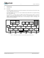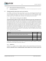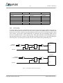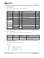
1
SPARC V8 32-bit Processor
LEON3 / LEON3-FT
CompanionCore Data Sheet
GAISLER
Features
Description
•
•
•
•
•
•
•
•
•
•
•
The LEON3 is a 32-bit processor based on the
SPARC V8 architecture. It implements a 7-stage
pipeline and separate instruction and data caches
(Harvard architecture). The number of register
windows is configurable within the limit of the
SPARC standard. A unique debug interface
allows non-intrusive hardware debugging and
provides access to all registers and memory.
SPARC V8 integer unit with 7-stage pipeline
Hardware multiply, divide and MAC units
Separate instruction and data caches
Support for 2 - 32 register windows
Radix-2 divider (non-restoring)
Single-vector trapping for reduced code size
Advanced debug support unit
Optional IEEE-STD-754 compliant FPU
20 DMIPS at 25 MHz system clock
Fault-tolerant version available
Support for Fusion, IGLOO, ProASIC3E/L,
RT ProASIC3, Axcelerator and RTAX
3-Port Register File
Trace Buffer
IEEE-754 FPU
Co-Processor
LEON3
7-Stage
Integer Pipeline
HW MUL/DIV
Local IRAM
ITLB
I-Cache
D-Cache
SRMMU
Debug port
Debug support unit
Interrupt port
Interrupt controller
Local DRAM
DTLB
AHB I/F
AMBA AHB Master (32-bit)
Applications
The LEON3 processor is designed for embedded
applications, combining high performance with
low complexity and low power consumption.
The LEON3 processor is highly configurable.
The fault-tolerant version of the LEON3
processor in combination with the radiation
tolerant Actel RTAX FPGA gives a total
immunity to radiation effects. This makes it
ideally suited for space and other high-rel
applications.
Copyright Aeroflex Gaisler AB
March 2010, Version 1.1
GAISLER
2
1
Introduction
1.1
Overview
LEON3 / LEON3-FT
The LEON3 SPARC V8 processor core has been designed to fit into architectures from which a large
variety of applications can be derived.
The LEON3 SPARC V8 processor core can be combined with the IEEE-STD-754 compliant Floating
Point Unit (GRFPU Lite).
The architecture is centered around the AMBA Advanced High-speed Bus (AHB), to which the
LEON3 core and other high-bandwidth units are connected. Low-bandwidth units connected to the
AMBA Advanced Peripheral Bus (APB) which is accessed through an AHB to APB bridge. The
architecture is shown in figure 1.
LEON3FT
32-bit SPARC
Integer Unit
I-cache D-cache
Interrupt
FPU
Debug
Support
Unit
UART
Debug
Link
JTAG
Debug
Link
On-Chip
Memory
with EDAC
Timers
2 x UART
16 x GPIO
AHB / APB
32-bit AMBA AHB
AHB
CTRL
Memory
Controller
with EDAC
32
PROM/SRAM
SDRAM
Controller
with EDAC
SpaceWire
Codec
Interface
CAN
2.0
Controller
LVDS I/F
CAN-2.0
Mil-Std-1553
BC/RT/MT
Interface
Mil-Std-1553
RT
Interface
Dual-1553
Dual-1553
32
SDRAM
Figure 1. Architectural block diagram of a typical system using the LEON3 processor
Copyright Aeroflex Gaisler AB
March 2010, Version 1.1
GAISLER
1.2
3
LEON3 / LEON3-FT
Signal overview
The LEON3 signals are shown in figure 2. Note that the AMBA AHB and debug signals are implemented VHDL records and are not shown in detail.
clk
Clock & Reset
rstn
irqi.irl[3:0]
irqo.irl[3:0]
Interrupt
irqi.rst
irqo.intack
irqi.run
dbgi
dbgo
Debug
ahbi
ahbo
AMBA
ahbsi
Figure 2. Signal overview
1.3
Implementation characteristics
The LEON3 processor is inherently portable and can be implemented on most FPGA and ASIC technologies. Table 1 shows the approximate cell count and frequency for different example configurations on Actel RTAX and RT ProASIC3, with 8 kbyte instruction and 4 kbyte data caches.
Table 1. Implementation characteristics (Cells / RAM blocks / AHB MHz)
Core configuration
LEON3
LEON3 + GRFPU Lite
LEON3-FT
LEON3-FT + GRFPU-FT Lite
RTAX2000S-1
RT ProASIC3
RT ProASIC3 with TMR
6500 / 31 / 25 MHz
-
-
13500 / 35 / 20 MHz
-
-
7500 / 31 / 25 MHz
8400 / 39 / 25 MHz
12300 / 39 / 25 MHz
14600 / 35 / 20 MHz
18200 / 47 / 20 MHz
24800 / 47 / 20 MHz
The LEON3 core is available in VHDL source code or as a pre-synthesized netlist.
The LEON3-FT core is available as a pre-synthesized netlist only.
Copyright Aeroflex Gaisler AB
March 2010, Version 1.1
GAISLER
4
LEON3 / LEON3-FT
2
LEON3 - High-performance SPARC V8 32-bit Processor
2.1
Overview
LEON3 is a 32-bit processor core conforming to the IEEE-1754 (SPARC V8) architecture. It is
designed for embedded applications, combining high performance with low complexity and low
power consumption.
The LEON3 core has the following main features: 7-stage pipeline with Harvard architecture, separate instruction and data caches, hardware multiplier and divider, on-chip debug support and multiprocessor extensions.
3-Port Register File
Trace Buffer
IEEE-754 FPU
Co-Processor
7-Stage
Integer pipeline
HW MUL/DIV
Local IRAM
ITLB
I-Cache
D-Cache
SRMMU
Debug port
Debug support unit
Interrupt port
Interrupt controller
Local DRAM
DTLB
AHB I/F
AMBA AHB Master (32-bit)
Figure 3. LEON3 processor core block diagram
Note: this manual describes the full functionality of the LEON3 core. Through the use of VHDL
generics, parts of the described functionality can be suppressed or modified to generate a smaller or
faster implementation.
2.1.1
Integer unit
The LEON3 integer unit implements the full SPARC V8 standard, including hardware multiply and
divide instructions. The number of register windows is configurable within the limit of the SPARC
standard (2 - 32), with a default setting of 8. The pipeline consists of 7 stages with a separate instruction and data cache interface (Harvard architecture).
2.1.2
Cache sub-system
LEON3 has a highly configurable cache system, consisting of a separate instruction and data cache.
Both caches can be configured with 1 - 4 sets, 1 - 256 kbyte/set, 16 or 32 bytes per line. Sub-blocking
is implemented with one valid bit per 32-bit word. The instruction cache uses streaming during linerefill to minimize refill latency. The data cache uses write-through policy and implements a doubleword write-buffer. The data cache can also perform bus-snooping on the AHB bus. A local scratch
Copyright Aeroflex Gaisler AB
March 2010, Version 1.1
GAISLER
5
LEON3 / LEON3-FT
pad ram can be added to both the instruction and data cache controllers to allow 0-waitstates access
memory without data write back.
2.1.3
Floating-point unit and co-processor
The LEON3 integer unit provides interfaces for a floating-point unit (FPU), and a custom co-processor. Two FPU controllers are available, one for the high-performance GRFPU (available from Gaisler
Research) and one for the Meiko FPU core (available from Sun Microsystems). The floating-point
processors and co-processor execute in parallel with the integer unit, and does not block the operation
unless a data or resource dependency exists.
2.1.4
Memory management unit
A SPARC V8 Reference Memory Management Unit (SRMMU) can optionally be enabled. The
SRMMU implements the full SPARC V8 MMU specification, and provides mapping between multiple 32-bit virtual address spaces and 36-bit physical memory. A three-level hardware table-walk is
implemented, and the MMU can be configured to up to 64 fully associative TLB entries.
2.1.5
On-chip debug support
The LEON3 pipeline includes functionality to allow non-intrusive debugging on target hardware. To
aid software debugging, up to four watchpoint registers can be enabled. Each register can cause a
breakpoint trap on an arbitrary instruction or data address range. When the (optional) debug support
unit is attached, the watchpoints can be used to enter debug mode. Through a debug support interface,
full access to all processor registers and caches is provided. The debug interfaces also allows single
stepping, instruction tracing and hardware breakpoint/watchpoint control. An internal trace buffer can
monitor and store executed instructions, which can later be read out over the debug interface.
2.1.6
Interrupt interface
LEON3 supports the SPARC V8 interrupt model with a total of 15 asynchronous interrupts. The interrupt interface provides functionality to both generate and acknowledge interrupts.
2.1.7
AMBA interface
The cache system implements an AMBA AHB master to load and store data to/from the caches. The
interface is compliant with the AMBA-2.0 standard. During line refill, incremental burst are generated to optimise the data transfer.
2.1.8
Power-down mode
The LEON3 processor core implements a power-down mode, which halts the pipeline and caches
until the next interrupt. This is an efficient way to minimize power-consumption when the application
is idle, and does not require tool-specific support in form of clock gating. To implement clock-gating,
a suitable clock-enable signal is produced by the processor.
2.1.9
Multi-processor support
LEON3 is designed to be use in multi-processor systems. Each processor has a unique index to allow
processor enumeration. The write-through caches and snooping mechanism guarantees memory
coherency in shared-memory systems.
Copyright Aeroflex Gaisler AB
March 2010, Version 1.1
GAISLER
6
LEON3 / LEON3-FT
2.1.10 Performance
Using 8K + 4K caches and a 16x16 multiplier, the dhrystone 2.1 benchmark reports 1.3 dhrystone
MIPS/MHz using the gcc-4.4.2 compiler (-O3 -mcpu=v8).
2.2
LEON3 integer unit
2.2.1
Overview
The LEON3 integer unit implements the integer part of the SPARC V8 instruction set. The implementation is focused on high performance and low complexity. The LEON3 integer unit has the following
main features:
•
7-stage instruction pipeline
•
Separate instruction and data cache interface
•
Support for 2 - 32 register windows
•
Hardware multiplier with optional 16x16 bit MAC and 40-bit accumulator
•
Radix-2 divider (non-restoring)
•
Single-vector trapping for reduced code size
Copyright Aeroflex Gaisler AB
March 2010, Version 1.1
GAISLER
7
LEON3 / LEON3-FT
Figure 4 shows a block diagram of the integer unit.
call/branch address
I-cache
+1
Add
‘0’ jmpa tbr
data address
f_pc
Fetch
d_inst
d_pc
r_inst
r_pc
Decode
r_imm
rd
register file
rs1
rs2
imm
Register Access
y, tbr, wim, psr
e_inst
e_pc
rs1
Execute
operand2
alu/shift
m_inst
mul/div
y
e pc
m_pc
result
30
jmpl address
32
32
address/dataout
datain
m_y
D-cache
Memory
x_inst
x_pc
xres
x_y
w_inst
w_pc
wres
Y
Exception
Write-back
30
tbr, wim, psr
Figure 4. LEON3 integer unit datapath diagram
2.2.2
Instruction pipeline
The LEON integer unit uses a single instruction issue pipeline with 7 stages:
1.
2.
3.
4.
5.
6.
7.
FE (Instruction Fetch): If the instruction cache is enabled, the instruction is fetched from the instruction cache.
Otherwise, the fetch is forwarded to the AHB bus. The instruction is valid at the end of this stage and is latched
inside the IU.
DE (Decode): The instruction is decoded and the CALL and Branch target addresses are generated.
RA (Register access): Operands are read from the register file or from internal data bypasses.
EX (Execute): ALU, logical, and shift operations are performed. For memory operations (e.g., LD) and for JMPL/
RETT, the address is generated.
ME (Memory): Data cache is read or written at this time.
XC (Exception) Traps and interrupts are resolved. For cache reads, the data is aligned as appropriate.
WR (Write): The result of any ALU, logical, shift, or cache operations are written back to the register file.
Copyright Aeroflex Gaisler AB
March 2010, Version 1.1
GAISLER
8
LEON3 / LEON3-FT
Table 2 lists the cycles per instruction (assuming cache hit and no icc or load interlock):
Table 2. Instruction timing
Instruction
Cycles (MMU disabled) Cycles (MMU fast-write)
JMPL, RETT
3
3
Cycles (MMU slow-write)
3
Double load
2
2
2
Single store
2
2
4
Double store
3
3
5
1/4*
1/4*
1/4*
SDIV/UDIV
35
35
35
Taken Trap
5
5
5
SMUL/UMUL
Atomic load/store
3
3
5
All other instructions
1
1
1
* Multiplication cycle count is 1 clock for the 32x32 multiplier and 4 clocks for the 16x16 version.
The processor pipeline can be configured for one or two cycles load delay. A branch interlock occurs
if an instruction that modifies the ICC bits in %psr is followed by a BICC or TICC instructions within
two clocks.
2.2.3
SPARC Implementor’s ID
Gaisler Research is assigned number 15 (0xF) as SPARC implementor’s identification. This value is
hard-coded into bits 31:28 in the %psr register. The version number for LEON3 is 3, which is hardcoded in to bits 27:24 of the %psr.
2.2.4
Divide instructions
Full support for SPARC V8 divide instructions is provided (SDIV, UDIV, SDIVCC & UDIVCC). The
divide instructions perform a 64-by-32 bit divide and produce a 32-bit result. Rounding and overflow
detection is performed as defined in the SPARC V8 standard.
2.2.5
Multiply instructions
The LEON processor supports the SPARC integer multiply instructions UMUL, SMUL UMULCC
and SMULCC. These instructions perform a 32x32-bit integer multiply, producing a 64-bit result.
SMUL and SMULCC performs signed multiply while UMUL and UMULCC performs unsigned
multiply. UMULCC and SMULCC also set the condition codes to reflect the result. The multiply
instructions are performed using a 32x32 pipelined hardware multiplier, or a 16x16 hardware multiplier which is iterated four times. To improve the timing, the 16x16 multiplier can optionally be provided with a pipeline stage.
2.2.6
Multiply and accumulate instructions
To accelerate DSP algorithms, two multiply&accumulate instructions are implemented: UMAC and
SMAC. The UMAC performs an unsigned 16-bit multiply, producing a 32-bit result, and adds the
result to a 40-bit accumulator made up by the 8 lsb bits from the %y register and the %asr18 register.
The least significant 32 bits are also written to the destination register. SMAC works similarly but performs signed multiply and accumulate. The MAC instructions execute in one clock but have two
Copyright Aeroflex Gaisler AB
March 2010, Version 1.1
GAISLER
9
LEON3 / LEON3-FT
clocks latency, meaning that one pipeline stall cycle will be inserted if the following instruction uses
the destination register of the MAC as a source operand.
Assembler syntax:
umacrs1, reg_imm, rd
smacrs1, reg_imm, rd
Operation:
prod[31:0] = rs1[15:0] * reg_imm[15:0]
result[39:0] = (Y[7:0] & %asr18[31:0]) + prod[31:0]
(Y[7:0] & %asr18[31:0]) = result[39:0]
rd = result[31:0]
%asr18 can be read and written using the RDASR and WRASR instructions.
2.2.7
Hardware breakpoints
The integer unit can be configured to include up to four hardware breakpoints. Each breakpoint consists of a pair of application-specific registers (%asr24/25, %asr26/27, %asr28/29 and %asr30/31)
registers; one with the break address and one with a mask:
31
%asr24, %asr26
%asr28, %asr30
2
WADDR[31:2]
31
%asr25, %asr27
%asr29, %asr31
0
IF
2
WMASK[31:2]
1
0
DL DS
Figure 5. Watch-point registers
Any binary aligned address range can be watched - the range is defined by the WADDR field, masked
by the WMASK field (WMASK[x] = 1 enables comparison). On a breakpoint hit, trap 0x0B is generated. By setting the IF, DL and DS bits, a hit can be generated on instruction fetch, data load or data
store. Clearing these three bits will effectively disable the breakpoint function.
2.2.8
Instruction trace buffer
The instruction trace buffer consists of a circular buffer that stores executed instructions. The trace
buffer operation is controlled through the debug support interface, and does not affect processor operation (see the DSU description). The size of the trace buffer is configurable from 1 to 64 kB through a
VHDL generic. The trace buffer is 128 bits wide, and stores the following information:
•
Instruction address and opcode
•
Instruction result
•
Load/store data and address
•
Trap information
•
30-bit time tag
Copyright Aeroflex Gaisler AB
March 2010, Version 1.1
GAISLER
10
LEON3 / LEON3-FT
The operation and control of the trace buffer is further described in section 29.4. Note that in multiprocessor systems, each processor has its own trace buffer allowing simultaneous tracing of all
instruction streams.
2.2.9
Processor configuration register
The application specific register 17 (%asr17) provides information on how various configuration
options were set during synthesis. This can be used to enhance the performance of software, or to support enumeration in multi-processor systems. The register can be accessed through the RDASR
instruction, and has the following layout:
31
%asr17
17 16 15 14 13 12 11 10 9
28
INDEX
RESERVED
CS
8
7
5 4
CF DW SV LD FPU M V8 NWP
0
NWIN
Figure 6. LEON3 configuration register (%asr17)
Field Definitions:
[31:28]: Processor index. In multi-processor systems, each LEON core gets a unique index to support enumeration. The
value in this field is identical to the hindex generic parameter in the VHDL model.
value in this field is identical to the hindex generic parameter in the VHDL model.
[17]:
Clock switching enabled (CS). If set switching between AHB and CPU frequency is available.
[16:15]: CPU clock frequency (CF). CPU core runs at (CF+1) times AHB frequency.
[14]:
Disable write error trap (DWT). When set, a write error trap (tt = 0x2b) will be ignored. Set to zero after reset.
[13]:
Single-vector trapping (SVT) enable. If set, will enable single-vector trapping. Fixed to zero if SVT is not
implemented. Set to zero after reset.
[12]:
Load delay. If set, the pipeline uses a 2-cycle load delay. Otherwise, a 1-cycle load delay i s used. Generated from
the lddel generic parameter in the VHDL model.
[11:10]: FPU option. “00” = no FPU; “01” = GRFPU; “10” = Meiko FPU, “11” = GRFPU-Lite
[9]:
If set, the optional multiply-accumulate (MAC) instruction is available
[8]:
If set, the SPARC V8 multiply and divide instructions are available.
[7:5]:
Number of implemented watchpoints (0 - 4)
[4:0]:
Number of implemented registers windows corresponds to NWIN+1.
Copyright Aeroflex Gaisler AB
March 2010, Version 1.1
GAISLER
11
LEON3 / LEON3-FT
2.2.10 Exceptions
LEON adheres to the general SPARC trap model. The table below shows the implemented traps and
their individual priority. When PSR (processor status register) bit ET=0, an exception trap causes the
processor to halt execution and enter error mode, and the external error signal will then be asserted.
Table 3. Trap allocation and priority
Trap
TT
Pri
Description
reset
0x00
1
Power-on reset
write error
0x2b
2
write buffer error during data store
instruction_access_error
0x01
3
Error during instruction fetch
illegal_instruction
0x02
5
UNIMP or other un-implemented instruction
privileged_instruction
0x03
4
Execution of privileged instruction in user mode
fp_disabled
0x04
6
FP instruction while FPU disabled
cp_disabled
0x24
6
CP instruction while Co-processor disabled
watchpoint_detected
0x0B
7
Hardware breakpoint match
window_overflow
0x05
8
SAVE into invalid window
window_underflow
0x06
8
RESTORE into invalid window
register_hadrware_error
0x20
9
register file EDAC error (LEON-FT only)
mem_address_not_aligned
0x07
10
Memory access to un-aligned address
fp_exception
0x08
11
FPU exception
cp_exception
0x28
11
Co-processor exception
data_access_exception
0x09
13
Access error during data load, MMU page fault
tag_overflow
0x0A
14
Tagged arithmetic overflow
divide_exception
0x2A
15
Divide by zero
interrupt_level_1
0x11
31
Asynchronous interrupt 1
interrupt_level_2
0x12
30
Asynchronous interrupt 2
interrupt_level_3
0x13
29
Asynchronous interrupt 3
interrupt_level_4
0x14
28
Asynchronous interrupt 4
interrupt_level_5
0x15
27
Asynchronous interrupt 5
interrupt_level_6
0x16
26
Asynchronous interrupt 6
interrupt_level_7
0x17
25
Asynchronous interrupt 7
interrupt_level_8
0x18
24
Asynchronous interrupt 8
interrupt_level_9
0x19
23
Asynchronous interrupt 9
interrupt_level_10
0x1A
22
Asynchronous interrupt 10
interrupt_level_11
0x1B
21
Asynchronous interrupt 11
interrupt_level_12
0x1C
20
Asynchronous interrupt 12
interrupt_level_13
0x1D
19
Asynchronous interrupt 13
interrupt_level_14
0x1E
18
Asynchronous interrupt 14
interrupt_level_15
0x1F
17
Asynchronous interrupt 15
trap_instruction
0x80 - 0xFF
16
Software trap instruction (TA)
Copyright Aeroflex Gaisler AB
March 2010, Version 1.1
GAISLER
12
LEON3 / LEON3-FT
2.2.11 Single vector trapping (SVT)
Single-vector trapping (SVT) is an SPARC V8e option to reduce code size for embedded applications.
When enabled, any taken trap will always jump to the reset trap handler (%tbr.tba + 0). The trap type
will be indicated in %tbr.tt, and must be decoded by the shared trap handler. SVT is enabled by setting
bit 13 in %asr17. The model must also be configured with the SVT generic = 1.
2.2.12 Address space identifiers (ASI)
In addition to the address, a SPARC processor also generates an 8-bit address space identifier (ASI),
providing up to 256 separate, 32-bit address spaces. During normal operation, the LEON3 processor
accesses instructions and data using ASI 0x8 - 0xB as defined in the SPARC standard. Using the
LDA/STA instructions, alternative address spaces can be accessed. The table shows the ASI usage for
LEON. Only ASI[5:0] are used for the mapping, ASI[7:6] have no influence on operation.
Table 4. ASI usage
ASI
Usage
0x01
Forced cache miss
0x02
System control registers (cache control register)
0x08, 0x09, 0x0A, 0x0B
Normal cached access (replace if cacheable)
0x0C
Instruction cache tags
0x0D
Instruction cache data
0x0E
Data cache tags
0x0F
Data cache data
0x10
Flush instruction cache
0x11
Flush data cache
2.2.13 Power-down
The processor can be configured to include a power-down feature to minimize power consumption
during idle periods. The power-down mode is entered by performing a WRASR instruction to
%asr19:
wr %g0, %asr19
During power-down, the pipeline is halted until the next interrupt occurs. Signals inside the processor
pipeline and caches are then static, reducing power consumption from dynamic switching.
2.2.14 Processor reset operation
The processor is reset by asserting the RESET input for at least 4 clock cycles. The following table
indicates the reset values of the registers which are affected by the reset. All other registers maintain
their value (or are undefined).
Table 5. Processor reset values
Register
Reset value
PC (program counter)
0x0
nPC (next program counter)
0x4
PSR (processor status register)
ET=0, S=1
Copyright Aeroflex Gaisler AB
March 2010, Version 1.1
GAISLER
13
LEON3 / LEON3-FT
By default, the execution will start from address 0. This can be overridden by setting the RSTADDR
generic in the model to a non-zero value. The reset address is always aligned on a 4 kbyte boundary. If
RSTADDR is set to 16#FFFFF#, then the reset address is taken from the signal IRQI.RSTVEC. This
allows the reset address to be changed dynamically.
2.2.15 Multi-processor support
The LEON3 processor support synchronous multi-processing (SMP) configurations, with up to 16
processors attached to the same AHB bus. In multi-processor systems, only the first processor will
start. All other processors will remain halted in power-down mode. After the system has been initialized, the remaining processors can be started by writing to the ‘MP status register’, located in the
multi-processor interrupt controller. The halted processors start executing from the reset address (0 or
RSTADDR generic). Enabling SMP is done by setting the smp generic to 1 or higher. Cache snooping
should always be enabled in SMP systems to maintain data cache coherency between the processors.
2.2.16 Cache sub-system
The LEON3 processor implements a Harvard architecture with separate instruction and data buses,
connected to two independent cache controllers. Both instruction and data cache controllers can be
separately configured to implement a direct-mapped cache or a multi-set cache with set associativity
of 2 - 4. The set size is configurable to 1 - 256 kbyte, divided into cache lines with 16 or 32 bytes of
data. In multi-set configurations, one of three replacement policies can be selected: least-recentlyused (LRU), least-recently-replaced (LRR) or (pseudo-) random. If the LRR algorithm can only be
used when the cache is 2-way associative. A cache line can be locked in the instruction or data cache
preventing it from being replaced by the replacement algorithm.
NOTE: The LRR algorithm uses one extra bit in tag rams to store replacement history. The LRU algorithm needs extra flip-flops per cache line to store access history. The random replacement algorithm
is implemented through modulo-N counter that selects which line to evict on cache miss.
Cachability for both caches is controlled through the AHB plug&play address information. The memory mapping for each AHB slave indicates whether the area is cachable, and this information is used
to (statically) determine which access will be treated as cacheable. This approach means that the cachability mapping is always coherent with the current AHB configuration. The AMBA plug&play cachability can be overriden using the CACHED generic. When this generic is not zero, it is treated as a
16-bit field, defining the cachability of each 256 Mbyte address block on the AMBA bus. A value of
16#00F3# will thus define cachable areas in 0 - 0x20000000 and 0x40000000 - 0x80000000.
2.2.17 AHB bus interface
The LEON3 processor uses one AHB master interface for all data and instruction accesses. Instructions are fetched with incremental bursts if the IB bit is set in the cache control register, otherwise single READ cycles are used. Data is accessed using byte, half-word and word accesses. A double load/
store data access will generate an incremental burst with two accesses.
The HPROT signals of the AHB bus are driven to indicate if the accesses is instruction or data, and if
it is a user or supervisor access.
Copyright Aeroflex Gaisler AB
March 2010, Version 1.1
GAISLER
2.3
14
LEON3 / LEON3-FT
Instruction cache
2.3.1
Operation
The instruction cache can be configured as a direct-mapped cache or as a multi-set cache with associativity of 2 - 4 implementing either LRU or random replacement policy or as 2-way associative
cache implementing LRR algorithm. The set size is configurable to 1 - 64 kbyte and divided into
cache lines of 16- 32 bytes. Each line has a cache tag associated with it consisting of a tag field, valid
field with one valid bit for each 4-byte sub-block and optional LRR and lock bits. On an instruction
cache miss to a cachable location, the instruction is fetched and the corresponding tag and data line
updated. In a multi-set configuration a line to be replaced is chosen according to the replacement policy.
If instruction burst fetch is enabled in the cache control register (CCR) the cache line is filled from
main memory starting at the missed address and until the end of the line. At the same time, the
instructions are forwarded to the IU (streaming). If the IU cannot accept the streamed instructions due
to internal dependencies or multi-cycle instruction, the IU is halted until the line fill is completed. If
the IU executes a control transfer instruction (branch/CALL/JMPL/RETT/TRAP) during the line fill,
the line fill will be terminated on the next fetch. If instruction burst fetch is enabled, instruction
streaming is enabled even when the cache is disabled. In this case, the fetched instructions are only
forwarded to the IU and the cache is not updated. During cache line refill, incremental burst are generated on the AHB bus.
If a memory access error occurs during a line fill with the IU halted, the corresponding valid bit in the
cache tag will not be set. If the IU later fetches an instruction from the failed address, a cache miss
will occur, triggering a new access to the failed address. If the error remains, an instruction access
error trap (tt=0x1) will be generated.
2.3.2
Instruction cache tag
A instruction cache tag entry consists of several fields as shown in figure 7:
Tag for 1 Kbyte set, 32 bytes/line
31
10
ATAG
9
8
7
0
VALID
LRR LOCK
Tag for 4 Kbyte set, 16bytes/line
31
12
ATAG
9
00
8
LRR LOCK
3
0000
0
VALID
Figure 7. Instruction cache tag layout examples
Field Definitions:
[31:10]:
[9]:
[8]:
[7:0]:
Address Tag (ATAG) - Contains the tag address of the cache line.
LRR - Used by LRR algorithm to store replacement history, otherwise 0.
LOCK - Locks a cache line when set. 0 if cache locking not implemented.
Valid (V) - When set, the corresponding sub-block of the cache line contains valid data. These bits are set when a
sub-block is filled due to a successful cache miss; a cache fill which results in a memory error will leave the valid
bit unset. A FLUSH instruction will clear all valid bits. V[0] corresponds to address 0 in the cache line, V[1] to
address 1, V[2] to address 2 and so on.
Copyright Aeroflex Gaisler AB
March 2010, Version 1.1
GAISLER
15
LEON3 / LEON3-FT
NOTE: only the necessary bits will be implemented in the cache tag, depending on the cache configuration. As an example, a 4 kbyte cache with 16 bytes per line would only have four valid bits and 20
tag bits. The cache rams are sized automatically by the ram generators in the model.
2.4
Data cache
2.4.1
Operation
The data cache can be configured as a direct-mapped cache or as a multi-set cache with associativity
of 2 - 4 implementing either LRU or (pseudo-) random replacement policy or as 2-way associative
cache implementing LRR algorithm. The set size is configurable to 1 - 64 kbyte and divided into
cache lines of 16 - 32 bytes. Each line has a cache tag associated with it consisting of a tag field, valid
field with one valid bit for each 4-byte sub-block and optional lock and LRR bits. On a data cache
read-miss to a cachable location 4 bytes of data are loaded into the cache from main memory. The
write policy for stores is write-through with no-allocate on write-miss. In a multi-set configuration a
line to be replaced on read-miss is chosen according to the replacement policy. Locked AHB transfers
are generated for LDST and SWAP instructions. If a memory access error occurs during a data load,
the corresponding valid bit in the cache tag will not be set. and a data access error trap (tt=0x9) will be
generated.
2.4.2
Write buffer
The write buffer (WRB) consists of three 32-bit registers used to temporarily hold store data until it is
sent to the destination device. For half-word or byte stores, the stored data replicated into proper byte
alignment for writing to a word-addressed device, before being loaded into one of the WRB registers.
The WRB is emptied prior to a load-miss cache-fill sequence to avoid any stale data from being read
in to the data cache.
Since the processor executes in parallel with the write buffer, a write error will not cause an exception
to the store instruction. Depending on memory and cache activity, the write cycle may not occur until
several clock cycles after the store instructions has completed. If a write error occurs, the currently
executing instruction will take trap 0x2b.
Note: the 0x2b trap handler should flush the data cache, since a write hit would update the cache while
the memory would keep the old value due the write error.
2.4.3
Data cache tag
A data cache tag entry consists of several fields as shown in figure 8:
31
10
ATAG
9
8
LRR LOCK
7
0
VALID
Figure 8. Data cache tag layout
Field Definitions:
[31:10]: Address Tag (ATAG) - Contains the address of the data held in the cache line.
[9]:
LRR - Used by LRR algorithm to store replacement history. ‘0’ if LRR is not used.
[8]:
LOCK - Locks a cache line when set. ‘0’ if instruction cache locking was not enabled in the configuration.
Copyright Aeroflex Gaisler AB
March 2010, Version 1.1
GAISLER
16
[3:0]:
LEON3 / LEON3-FT
Valid (V) - When set, the corresponding sub-block of the cache line contains valid data. These bits are set when a
sub-block is filled due to a successful cache miss; a cache fill which results in a memory error will leave the valid
bit unset. V[0] corresponds to address 0 in the cache line, V[1] to address 1, V[2] to address 2 and V[3] to address 3.
NOTE: only the necessary bits will be implemented in the cache tag, depending on the cache configuration. As an example, a 2 kbyte cache with 32 bytes per line would only have eight valid bits and 21
tag bits. The cache rams are sized automatically by the ram generators in the model.
2.5
Additional cache functionality
2.5.1
Cache flushing
Both instruction and data cache are flushed by executing the FLUSH instruction. The instruction
cache is also flushed by setting the FI bit in the cache control register, or by writing to any location
with ASI=0x15. The data cache is also flushed by setting the FD bit in the cache control register, or by
writing to any location with ASI=0x16. Cache flushing takes one cycle per cache line, during which
the IU will not be halted, but during which the caches are disabled. When the flush operation is completed, the cache will resume the state (disabled, enabled or frozen) indicated in the cache control register. Diagnostic access to the cache is not possible during a FLUSH operation and will cause a data
exception (trap=0x09) if attempted.
2.5.2
Diagnostic cache access
Tags and data in the instruction and data cache can be accessed through ASI address space 0xC, 0xD,
0xE and 0xF by executing LDA and STA instructions. Address bits making up the cache offset will be
used to index the tag to be accessed while the least significant bits of the bits making up the address
tag will be used to index the cache set.
Diagnostic read of tags is possible by executing an LDA instruction with ASI=0xC for instruction
cache tags and ASI=0xE for data cache tags. A cache line and set are indexed by the address bits making up the cache offset and the least significant bits of the address bits making up the address tag. Similarly, the data sub-blocks may be read by executing an LDA instruction with ASI=0xD for instruction
cache data and ASI=0xF for data cache data. The sub-block to be read in the indexed cache line and
set is selected by A[4:2].
The tags can be directly written by executing a STA instruction with ASI=0xC for the instruction
cache tags and ASI=0xE for the data cache tags. The cache line and set are indexed by the address bits
making up the cache offset and the least significant bits of the address bits making up the address tag.
D[31:10] is written into the ATAG field (see above) and the valid bits are written with the D[7:0] of
the write data. Bit D[9] is written into the LRR bit (if enabled) and D[8] is written into the lock bit (if
enabled). The data sub-blocks can be directly written by executing a STA instruction with ASI=0xD
for the instruction cache data and ASI=0xF for the data cache data. The sub-block to be read in the
indexed cache line and set is selected by A[4:2].
In multi-way caches, the address of the tags and data of the ways are concatenated. The address of a
tag or data is thus:
ADDRESS = WAY & LINE & DATA & “00”
Examples: the tag for line 2 in way 1 of a 2x4 Kbyte cache with 16 byte line would be:
A[13:12]
=1
(WAY)
A[11:5]
=2
(TAG)
Copyright Aeroflex Gaisler AB
March 2010, Version 1.1
GAISLER
17
LEON3 / LEON3-FT
=> TAG ADDRESS = 0x1040
The data of this line would be at addresses 0x1040 - 0x104C
2.5.3
Cache line locking
In a multi-set configuration the instruction and data cache controllers can be configured with optional
lock bit in the cache tag. Setting the lock bit prevents the cache line to be replaced by the replacement
algorithm. A cache line is locked by performing a diagnostic write to the instruction tag on the cache
offset of the line to be locked setting the Address Tag field to the address tag of the line to be locked,
setting the lock bit and clearing the valid bits. The locked cache line will be updated on a read-miss
and will remain in the cache until the line is unlocked. The first cache line on certain cache offset is
locked in the set 0. If several lines on the same cache offset are to be locked the locking is performed
on the same cache offset and in sets in ascending order starting with set 0. The last set can not be
locked and is always replaceable. Unlocking is performed in descending set order.
NOTE: Setting the lock bit in a cache tag and reading the same tag will show if the cache line locking
was enabled during the LEON3 configuration: the lock bit will be set if the cache line locking was
enabled otherwise it will be 0.
2.5.4
Local instruction ram
A local instruction ram can optionally be attached to the instruction cache controller. The size of the
local instruction is configurable from 1-256 kB. The local instruction ram can be mapped to any 16
Mbyte block of the address space. When executing in the local instruction ram all instruction fetches
are performed from the local instruction ram and will never cause IU pipeline stall or generate an
instruction fetch on the AHB bus. Local instruction ram can be accessed through load/store integer
word instructions (LD/ST). Only word accesses are allowed, byte, halfword or double word access to
the local instruction ram will generate data exception.
2.5.5
Local scratch pad ram
Local scratch pad ram can optionally be attached to both instruction and data cache controllers. The
scratch pad ram provides fast 0-waitstates ram memories for both instructions and data. The ram can
be between 1 - 256 kbyte, and mapped on any 16 Mbyte block in the address space. Accessed performed to the scratch pad ram are not cached, and will not appear on the AHB bus. The scratch pads
rams do not appear on the AHB bus, and can only be read or written by the processor. The instruction
ram must be initialized by software (through store instructions) before it can be used. The default
address for the instruction ram is 0x8e000000, and for the data ram 0x8f000000. See section 2.10 for
additional configuration details. Note: local scratch pad ram can only be enabled when the MMU is
disabled.
2.5.6
Data Cache snooping
To keep the data cache synchronized with external memory, cache snooping can be enabled through
the dsnoop generic. When enabled, the data cache monitors write accesses on the AHB bus to cacheable locations. If an other AHB master writes to a cacheable location which is currently cached in the
data cache, the corresponding cache line is marked as invalid.
2.5.7
Cache Control Register
The operation of the instruction and data caches is controlled through a common Cache Control Register (CCR) (figure 9). Each cache can be in one of three modes: disabled, enabled and frozen. If dis-
Copyright Aeroflex Gaisler AB
March 2010, Version 1.1
GAISLER
18
LEON3 / LEON3-FT
abled, no cache operation is performed and load and store requests are passed directly to the memory
controller. If enabled, the cache operates as described above. In the frozen state, the cache is accessed
and kept in sync with the main memory as if it was enabled, but no new lines are allocated on read
misses.
31
23 22 21
16 15 14
DS FD FI
IB IP DP
6
5
4 3
2
DF IF DCS
1
0
ICS
Figure 9. Cache control register
[23]:
[22]:
[21]:
[16]:
[15]:
[14]:
[5]:
[4]:
[3:2]:
[1:0]:
Data cache snoop enable [DS] - if set, will enable data cache snooping.
Flush data cache (FD). If set, will flush the instruction cache. Always reads as zero.
Flush Instruction cache (FI). If set, will flush the instruction cache. Always reads as zero.
Instruction burst fetch (IB). This bit enables burst fill during instruction fetch.
Instruction cache flush pending (IP). This bit is set when an instruction cache flush operation is in progress.
Data cache flush pending (DP). This bit is set when an data cache flush operation
is in progress.
Data Cache Freeze on Interrupt (DF) - If set, the data cache will automatically be frozen when an asynchronous
interrupt is taken.
Instruction Cache Freeze on Interrupt (IF) - If set, the instruction cache will automatically be frozen when an
asynchronous interrupt is taken.
Data Cache state (DCS) - Indicates the current data cache state according to the following: X0= disabled, 01 =
frozen, 11 = enabled.
Instruction Cache state (ICS) - Indicates the current data cache state according to the
following: X0= disabled, 01 = frozen, 11 = enabled.
If the DF or IF bit is set, the corresponding cache will be frozen when an asynchronous interrupt is
taken. This can be beneficial in real-time system to allow a more accurate calculation of worst-case
execution time for a code segment. The execution of the interrupt handler will not evict any cache
lines and when control is returned to the interrupted task, the cache state is identical to what it was
before the interrupt. If a cache has been frozen by an interrupt, it can only be enabled again by
enabling it in the CCR. This is typically done at the end of the interrupt handler before control is
returned to the interrupted task.
2.5.8
Cache configuration registers
The configuration of the two caches if defined in two registers: the instruction and data configuration
registers. These registers are read-only and indicate the size and configuration of the caches.
31
CL
30 29 28 27 26 25 24 23
REPL SN
SETS
20 19 18
SSIZE
LR
LSIZE
16 15
12 11
LRSIZE
4 3
LRSTART
0
M
Figure 10. Cache configuration register
[31]:
Cache locking (CL). Set if cache locking is implemented.
[29:28]: Cache replacement policy (REPL). 00 - no replacement policy (direct-mapped cache), 01 - least recently used
(LRU), 10 - least recently replaced (LRR), 11 - random
[27]:
Cache snooping (SN). Set if snooping is implemented.
[26:24]: Cache associativity (SETS). Number of sets in the cache: 000 - direct mapped, 001 - 2-way associative, 010 - 3-way
associative, 011 - 4-way associative
[23:20]: Set size (SSIZE). Indicates the size (Kbytes) of each cache set. Size = 2SIZE
Copyright Aeroflex Gaisler AB
March 2010, Version 1.1
GAISLER
19
LEON3 / LEON3-FT
[19]:
Local ram (LR). Set if local scratch pad ram is implemented.
[18:16]: Line size (LSIZE). Indicated the size (words) of each cache line. Line size = 2LSZ
[15:12]: Local ram size (LRSZ). Indicates the size (Kbytes) of the implemented local scratch pad ram. Local ram size =
2LRSZ
[11:4]: Local ram start address. Indicates the 8 most significant bits of the local ram start address.
[3]:
MMU present. This bit is set to ‘1’ if an MMU is present.
All cache registers are accessed through load/store operations to the alternate address space (LDA/
STA), using ASI = 2. The table below shows the register addresses:
Table 6. ASI 2 (system registers) address map
Address
Register
0x00
Cache control register
0x04
Reserved
0x08
Instruction cache configuration register
0x0C
Data cache configuration register
2.5.9
Software consideration
After reset, the caches are disabled and the cache control register (CCR) is 0. Before the caches may
be enabled, a flush operation must be performed to initialized (clear) the tags and valid bits. A suitable
assembly sequence could be:
flush
set 0x81000f, %g1
sta%g1, [%g0] 2
2.6
Memory management unit
A SPARC V8 reference MMU (SRMMU) can optionally be enabled in the LEON3 configuartion. For
details on the SRMMU operation, see the SPARC V8 manual.
2.6.1
MMU/Cache operation
When the MMU is disabled, the MMU is bypassed and the caches operate with physical address mapping. When the MMU is enabled, the caches tags store the virtual address and also include an 8-bit
context field. Both the tag address and context field must match to generate a cache hit.
If cache snooping is desired when the MMU is enabled, bit 2 of the dsnoop generic must be set. This
will also store the physical address in each cache tag, which is then used for snooping. The size of
each data cache way has to be smaller or equal to the MMU page size, which typically is 4 Kbyte (see
below). This is necessary to avoid aliasing in the cache since the virtual tags are indexed with a virtual
offset while the physical tags are indexed with a physical offset. Physical tags and snoop support is
needed for SMP systems using the MMU (linux-2.6).
Because the cache is virtually tagged, no extra clock cycles are needed in case of a cache load hit. In
case of a cache miss or store hit (write-through cache), 2 extra clock cycles are used to generate the
physical address if there is a TLB hit. If there is a TLB miss the page table must be traversed, resulting
in up to four AMBA read accesses and one possible writeback operation. If a combined TLB is used
by the instruction cache, the translation is stalled until the TLB is free. If fast TLB operation is
selected (tlb_type = 2), the TLB will be accessed simultaneously with tag access, saving 2 clocks on
Copyright Aeroflex Gaisler AB
March 2010, Version 1.1
GAISLER
20
LEON3 / LEON3-FT
cache miss. This will increase the area somewhat, and may reduce the timing, but usually results in
better overall throughput.
An MMU page fault will generate trap 0x09, and update the MMU status registers as defined in the
SPARC V8 Manual. The cache and memory will not be modified on an MMU page fault.
2.6.2
Translation look-aside buffer (TLB)
The MMU can be configured to use a shared TLB, or separate TLB for instructions and data. The
number of TLB entries can be set to 2 - 32 in the configuration record. The organisation of the TLB
and number of entries is not visible to the software and does thus not require any modification to the
operating system.
2.6.3
Variable minimum page sizes
The standard minimum page size for the SRMMU is 4 Kbyte. The minimum page size can also be
configured to 8, 16 or 32 Kbyte in order to allow for large data cache ways. The page sizes for level 1,
2 and 3 is seen in the table below:
Table 7. MMU pagse size
Scheme
Level-1
Level-2
Level-3
4 Kbyte (default)
16 Mbyte
256 Kbyte
4 Kbyte
8 Kbyte
32 Mbyte
512 Kbyte
8 Kbyte
16 Kbyte
64 Mbyte
1 Mbyte
16 Kbyte
32 Kbyte
256 Mbyte
2 Mbyte
32 Kbyte
The layouts of the indexes are choosen so that PTE pagetables can be joined together inside one
MMU page without leaving holes. The page size can optionally also be choosen by the program at
run-time by setting generic mmupgsz to 1. In this case the page size is choosen by bit [17:16] in the
MMU control register.
2.6.4
MMU registers
The following MMU registers are implemented:
Table 8. MMU registers (ASI = 0x19)
Address
Register
0x000
MMU control register
0x100
Context pointer register
0x200
Context register
0x300
Fault status register
0x400
Fault address register
The MMU control register layout can be seen below, while the definition of the remaning MMU registers can be found in the SPARC V8 manual.
Copyright Aeroflex Gaisler AB
March 2010, Version 1.1
GAISLER
21
LEON3 / LEON3-FT
.
31
28 27
IMPL
24 23
VER
21 20
ITLB
18
DTLB
17 16 15
PSZ
14
2 1
TD ST
RESERVED
0
NF E
Figure 11. MMU control register
[31:28]: MMU Implementation ID. Hardcoded to “0000”..
[27:24]: MMU Version ID. Hardcoded to “0001”.
[23:21]: Number of ITLB entires. The number of ITLB entries is calculated as 2ITLB. If the TLB is shared between
instructions and data, this filed indicates to total number of TLBs.
[20:18]: Number of DTLB entires. The number of DTLB entries is calculated as 2DTLB. If the TLB is shared between
instructions and data, this filed is zero.
[17:16]: Page size. The size of the smallest MMU page. 0 = 4 Kbyte; 1 = 8 Kbyte; 2 = 16 Kbyte; 3 = 32 Kbyte. If the page
size is programmable, this field is writable, otherwise it is read-only.
[15]:
TLB disable. When set to 1, the TLB will be disabled and each data access will generate an MMU page table walk.
[14]:
Separate TLB. This bit is set to 1 if separate instructions and data TLM are implemented.
[1]:
No Fault. When NF= 0, any fault detected by the MMU causes FSR and FAR to be updated and causes a fault to be
generated to the processor. When NF= 1, a fault on an access to ASI 9 is handled as when NF= 0; a fault on an access
to any other ASI causes FSR and FAR to be updated but no fault is generated to the processor.
[0]:
Enable MMU. 0 = MMU disabled, 1 = MMU enabled.
2.6.5
ASI mappings
When the MMU is used, the following ASI mappings are added:
Table 9. MMU ASI usage
ASI
Usage
0x10
Flush page
0x10
MMU flush page
0x13
MMU flush context
0x14
MMU diagnostic dcache context access
0x15
MMU diagnostic icache context access
0x19
MMU registers
0x1C
MMU bypass
0x1D
MMU diagnostic access
0x1E
MMU snoop tags diagnostic access
2.6.6
Snoop tag diagnostic access
If the MMU has been configured to use separate snoop tags, they can be accessed via ASI 0x1E. This
is primarily useful for RAM testing, and should not be performed during normal operation. The figure
below shows the layout of the snoop tag for a 1 Kbyte data cache:
31
10
ATAG
9
2
“0000”
1
PAR
0
IV
Figure 12. Snoop cache tag layout
Copyright Aeroflex Gaisler AB
March 2010, Version 1.1
GAISLER
22
LEON3 / LEON3-FT
[31:10] Address tag. The physical address tag of the cache line.
[1]:
Parity. The odd parity over the data tag. LEON3FT only.
[0]:
Invalid. When set, the cache line is not valid and will cause a cache miss if accessed by the processor. Only present
if fast snooping is enabled.
2.7
Floating-point unit and custom co-processor interface
The SPARC V8 architecture defines two (optional) co-processors: one floating-point unit (FPU) and
one user-defined co-processor. Two different FPU’s can be interfaced the LEON3 pipeline: Gaisler
Research’s GRFPU and GRFPU-Lite. Selection of which FPU to use is done through the VHDL
model’s generic map. The characteristics of the FPU’s are described in the next sections.
2.7.1
Gaisler Research’s floating-point unit (GRFPU)
The high-performance GRFPU operates on single- and double-precision operands, and implements all
SPARC V8 FPU instructions. The FPU is interfaced to the LEON3 pipeline using a LEON3-specific
FPU controller (GRFPC) that allows FPU instructions to be executed simultaneously with integer
instructions. Only in case of a data or resource dependency is the integer pipeline held. The GRFPU is
fully pipelined and allows the start of one instruction each clock cycle, with the exception is FDIV
and FSQRT which can only be executed one at a time. The FDIV and FSQRT are however executed
in a separate divide unit and do not block the FPU from performing all other operations in parallel.
All instructions except FDIV and FSQRT has a latency of three cycles, but to improve timing, the
LEON3 FPU controller inserts an extra pipeline stage in the result forwarding path. This results in a
latency of four clock cycles at instruction level. The table below shows the GRFPU instruction timing
when used together with GRFPC:
Table 10. GRFPU instruction timing with GRFPC
Instruction
Throughput
Latency
FADDS, FADDD, FSUBS, FSUBD,FMULS, FMULD, FSMULD, FITOS, FITOD,
FSTOI, FDTOI, FSTOD, FDTOS, FCMPS, FCMPD, FCMPES. FCMPED
1
4
FDIVS
14
16
FDIVD
15
17
FSQRTS
22
24
FSQRTD
23
25
The GRFPC controller implements the SPARC deferred trap model, and the FPU trap queue (FQ) can
contain up to 7 queued instructions when an FPU exception is taken. When the GRFPU is enabled in
the model, the version field in %fsr has the value of 2.
2.7.2
GRFPU-Lite
GRFPU-Lite is a smaller version of GRFPU, suitable for FPGA implementations with limited logic
resources. The GRFPU-Lite is not pipelined and executes thus only one instruction at a time. To
improve performance, the FPU controller (GRLFPC) allows GRFPU-Lite to execute in parallel with
Copyright Aeroflex Gaisler AB
March 2010, Version 1.1
GAISLER
23
LEON3 / LEON3-FT
the processor pipeline as long as no new FPU instructions are pending. Below is a table of worst-case
throughput of the GRFPU-Lite:
Table 11. GRFPU-Lite worst-case instruction timing with GRLFPC
Instruction
Throughput
Latency
FADDS, FADDD, FSUBS, FSUBD,FMULS, FMULD, FSMULD, FITOS, FITOD,
FSTOI, FDTOI, FSTOD, FDTOS, FCMPS, FCMPD, FCMPES. FCMPED
8
8
FDIVS
31
31
FDIVD
57
57
FSQRTS
46
46
FSQRTD
65
65
When the GRFPU-Lite is enabled in the model, the version field in %fsr has the value of 3.
2.8
Vendor and device identifiers
The core has vendor identifiers 0x01 (Gaisler Research) and device identifiers 0x003. For description
of vendor and device identifiers see GRLIB IP Library User’s Manual.
2.9
Implementation
2.9.1
Area and timing
Both area and timing of the LEON3 core depends strongly on the selected configuration, target technology and the used synthesis tool. The table below indicates the typical figures for two baseline configurations.
Table 12. Area and timing
Actel AX2000
ASIC (0.13 um)
Configuration
Cells
RAM64
MHz
Gates
MHz
LEON3, 8 + 8 Kbyte cache
6,500
40
30
25,000
400
LEON3, 8 + 8 Kbyte cache + DSU3
7,500
40
25
30,000
400
2.9.2
Technology mapping
LEON3 has two technology mapping generics, fabtech and memtech. The fabtech generic controls the
implementation of some pipeline features, while memtech selects which memory blocks will be used
to implement cache memories and the IU/FPU register file. Fabtech can be set to any of the provided
technologies (0 - NTECH) as defined in the GRPIB.TECH package. See the GRLIB Users’s Manual
for available settings for memtech.
2.9.3
RAM usage
The LEON3 core maps all usage of RAM memory on the syncram, syncram_2p and syncram_dp
components from the technology mapping library (TECHMAP). The type, configuration and number
of RAM blocks is described below.
Register file
Copyright Aeroflex Gaisler AB
March 2010, Version 1.1
GAISLER
24
LEON3 / LEON3-FT
The register file is implemented with two synram_2p blocks for all technologies where the
regfile_3p_infer constant in TECHMAP.GENCOMP is set to 0. The organization of the syncram_2p
is shown in the following table:
Table 13. syncram_2p sizes for LEON3 register file
Register windows
Syncram_2p organization
2-3
64x32
4-7
128x32
8 - 15
256x32
16-31
512x31
32
1024x32
If regfile_3p_infer is set to 1, the synthesis tool will automatically infer the register. On FPGA technologies, it can be in either flip-flops or RAM cells, depending on the tool and technology. On ASIC
technologies, it will be flip-flops. The amount of flip-flops inferred is equal to the number of registers:
Number of flip-flops = ((NWINDOWS *16) + 8) * 32
FP register file
If FPU support is enabled, the FP register file is implemented with four synram_2p blocks when the
regfile_3p_infer constant in TECHMAP.GENCOMP is set to 0. The organization of the syncram_2p
blocks is 16x32.
If regfile_3p_infer is set to 1, the synthesis tool will automatically infer the FP register file. For ASIC
technologies the number of inferred flip-flops is equal to number of bits in the FP register file which is
32 * 32 = 1024.
Cache memories
RAM blocks are used to implement the cache tags and data memories. Depending on cache configuration, different types and sizes of RAM blocks are used.
The tag memory is implemented with one syncram per cache way when no snooping is enabled. The
tag memory depth and width is calculated as follows:
Depth = (cache way size in bytes) / (cache line size in bytes)
Width = 32 - log2(cache way size in bytes) + (cache line size in bytes)/4 + lrr + lock
For a 2 Kbyte cache way with lrr replacement and 32 bytes/line, the tag RAM depth will be (2048/32)
= 64. The width will be: 32 - log2(2048) + 32/4 + 1 = 32 - 11 + 8 + 1 = 28. The tag RAM organization
will thus be 64x28 for the configuration. If the MMU is enabled, the tag memory width will increase
with 8 to store the process context ID, and the above configuration will us a 64x36 RAM.
If snooping is enabled, the tag memories will be implemented using the syncram_dp component
(dual-port RAM). One port will be used by the processor for cache access/refill, while the other port
will be used by the snooping and invalidation logic. The size of the syncram_dp block will be the
same as when snooping is disabled. If physical snooping is enabled (separate snoop tags), one extra
RAM block per data way will be instatiated to hold the physical tags. The width of the RAM block
will be the same as the tag address: 32 - log2(way size). A 4 Kbyte data cache way will thus require a
32 - 12 = 20 bit wide RAM block for the physical tags. If fast snooping is enabled, the tag RAM (vir-
Copyright Aeroflex Gaisler AB
March 2010, Version 1.1
GAISLER
25
LEON3 / LEON3-FT
tual and physical) will be implemented using syncram_2p instead of syncram_dp. This can be used to
implement snooping on technologies which lack dual-port RAM but have 2-port RAM.
The data part of the caches (storing instructions or data) is always 32 bit wide. The depth is equal to
the way size in bytes, divided by 4. A cache way of 2 Kbyte will thus use syncram component with
and organization of 512x32.
Instruction Trace buffer
The instruction trace buffer will use four identical RAM blocks (syncram) to implement the buffer
memory. The syncrams will always be 32-bit wide. The depth will depend on the TBUF generic,
which indicates the total size of trace buffer in Kbytes. If TBUF = 1 (1 Kbyte), then four RAM blocks
of 64x32 will be used. If TBUF = 2, then the RAM blocks will be 128x32 and so on.
Scratch pad RAM
If the instruction scratch pad RAM is enabled, a syncram block will be instantiated with a 32-bit data
width. The depth of the RAM will correspond to the configured scratch pad size. An 8 Kbyte scratch
pad will use a syncram with 2048x32 organization. The RAM block for the data scratch pad will be
configured in the same way as the instruction scratch pad.
2.9.4
Double clocking
The LEON3 CPU core be clocked at twice the clock speed of the AMBA AHB bus. When clocked at
double AHB clock frequency, all CPU core parts including integer unit and caches will operate at
double AHB clock frequency while the AHB bus access is performed at the slower AHB clock frequency. The two clocks have to be synchronous and a multicycle paths between the two clock
domains have to be defined at synthesis tool level. A separate component (leon3s2x) is provided for
the double clocked core. Double clocked versions of DSU (dsu3_2x) and MP interrupt controller
(irqmp2x) are used in a double clocked LEON3 system. An AHB clock qualifier signal (clken input)
is used to identify end of AHB cycle. The AHB qualifier signal is generated in CPU clock domain and
is high during the last CPU clock cycle under AHB clock low-phase. Sample leon3-clk2x design provides a module that generates an AHB clock qualifier signal.
Double-clocked design has two clock domains: AMBA clock domains (HCLK) and CPU clock
domain (CPUCLK). LEON3 (leon3s2x component) and DSU3 (dsu3_2x) belong to CPU clock
domain (clocked by CPUCLK), while the rest of the system is in AMBA clock domain (clocked by
HCLK). Paths between the two clock domains (paths starting in CPUCLK domain and ending in
HCLK and paths starting in HCLK domain and ending in CPUCLK domain) are multicycle paths
with propagation time of two CPUCLK periods (or one HCLK period) with following exceptions:
Start point
Through
End point
Propagation time
CPUCLK
ahbi
CPUCLK
2 CPUCLK
CPUCLK
ahbsi
CPUCLK
2 CPUCLK
CPUCLK
ahbso
CPUCLK
2 CPUCLK
HCLK
irqi
CPUCLK
1 CPUCLK
CPUCLK
irqo
HCLK
1 CPUCLK
u0_0/p0/c0/sync0/r[*]
(register)
1 CPUCLK
leon3s2x core
CPUCLK
Copyright Aeroflex Gaisler AB
March 2010, Version 1.1
GAISLER
26
Start point
Through
LEON3 / LEON3-FT
End point
Propagation time
dsu3_2x core
CPUCLK
ahbmi
CPUCLK
2 CPUCLK
CPUCLK
ahbsi
CPUCLK
2 CPUCLK
dsui
CPUCLK
1 CPUCLK
rh[*] (register)
1 CPUCLK
r[*] (register)
1 CPUCLK
r[*] (register)
irqmp2x core
r2[*] (register)
2.9.5
Clock gating
To further reduce the power consumption of the processor, the clock can be gated-off when the processor has entered power-down state. Since the cache controllers and MMU operate in parallel with
the processor, the clock cannot be gated immediately when the processor has entered the power-down
state. Instead, a power-down signal (DBGO.idle) is generated when all outstanding AHB accesses
have been completed and it is safe to gate the clock. This signal should be clocked though a positiveedge flip-flop followed by a negative-edge flip-flop to guarantee that the clock is gated off during the
clock-low phase. To ensure proper start-up state, the clock should not be gated during reset.
LEON3CG
RESETN
DBGO.IDLE
D
Q
D
Q
GCLK
CLK
AHB CLK
LEON3CG
RESETN
DSUO.PWD[n]
D
Q
GCLK
CLK
AHB CLK
Figure 13. Examples of LEON3 clock gating
Copyright Aeroflex Gaisler AB
March 2010, Version 1.1
GAISLER
27
LEON3 / LEON3-FT
The processor should exit the power-down state when an interrupt become pending. The signal
DBGO.ipend will then go high when this happen, and should be used to re-enable the clock.
When the debug support unit (DSU3) is used, the DSUO.pwd signal should be used instead of
DBGO.idle. This will ensure that the clock also is re-enabled when the processor is switched from
power-down to debug state by the DSU. The DSUO.pwd is a vector with one power-down signal per
CPU (for SMP systems). DSUO.pwd takes DBGO.ipend into account, and no further gating or latching needs to be done of this signal. If cache snooping has been enabled, the continuous clock will
ensure that the snooping logic is activated when necessary and will keep the data cache synchronized
even when the processor clock is gated-off. In a multi-processor system, all processor except node 0
will enter power-down after reset and will allow immediate clock-gating without additional software
support.
Clock-tree routing must ensure that the continuous clock (CLK) and the gated clock (GCLK) are
phase-aligned. The template design leon3-clock-gating shows an example of a clock-gated system.
The leon3cg entity should be used when clock gating is implemented. This entity has one input more
(GCLK) which should be driven by the gated clock. Using the double-clocked version of leon3
(leon3s2x), the GCLK2 is the gated double-clock while CLK and CLK2 should be continuous.
2.9.6
Scan support
If the SCANTEST generic is set to 1, support for scan testing is enabled. This will make use of the
AHB scan support signals in the following manner: when AHBI.testen and AHBI.scanen are both ‘1’,
the select signals to all RAM blocks (cache RAM, register file and DSU trace buffers) are disabled.
This means that when the scan chain is shifted, no accidental write or read can occur in the RAM
blocks. The scan signal AHBI.testrst is not used as there are no asynchronous resets in the LEON3
core.
Copyright Aeroflex Gaisler AB
March 2010, Version 1.1
GAISLER
2.10
28
LEON3 / LEON3-FT
Configuration options
Table 14 shows the configuration options of the core (VHDL generics).
Table 14. Configuration options
Generic
Function
Allowed range
hindex
AHB master index
0 - NAHBMST-1 0
Default
fabtech
Target technology
0 - NTECH
0 (inferred)
memtech
Vendor library for regfile and cache RAMs
0 - NTECH
0 (inferred)
nwindows
Number of SPARC register windows. Choose 8 windows to be
compatible with Bare-C and RTEMS cross-compilers.
2 - 32
8
dsu
Enable Debug Support Unit interface
0-1
0
fpu
Floating-point Unit
0 - 31
0
0 - 16#3F#
0
0 : no FPU
1 - 7: GRFPU 1 - inferred multiplier, 2 - DW multiplier, 3 - Module Generator multiplier, 4 - Technology specific multiplier
8 - 14: GRFPU-Lite 8 - simple FPC, 9 - data forwarding FPC, 10
- non-blocking FPC
15: Meiko
16 - 31: as above (modulo 16) but use netlist
v8
Generate SPARC V8 MUL and DIV instructions
0 : No multiplier or divider
1 : 16x16 multiplier
2 : 16x16 pipelined multiplier
16#32# : 32x32 pipelined multiplier
cp
Generate co-processor interface
0 -1
0
mac
Generate SPARC V8e SMAC/UMAC instruction
0-1
0
pclow
Least significant bit of PC (Program Counter) that is actually
generated. PC[1:0] are always zero and are normally not generated. Generating PC[1:0] makes VHDL-debugging easier.
0, 2
2
notag
Currently not used
-
-
nwp
Number of watchpoints
0-4
0
icen
Enable instruction cache
0-1
1
Instruction cache replacement policy.
0-1
0
irepl
0 - least recently used (LRU), 1 - least recently replaced (LRR),
2 - random
isets
Number of instruction cache sets
1-4
1
ilinesize
Instruction cache line size in number of words
4, 8
4
isetsize
Size of each instruction cache set in kByte
1 - 256
1
isetlock
Enable instruction cache line locking
0-1
0
dcen
Data cache enable
0-1
1
drepl
Data cache replacement policy.
0-1
0
0 - least recently used (LRU), 1 - least recently replaced (LRR),
2 - random
dsets
Number of data cache sets
1-4
1
dlinesize
Data cache line size in number of words
4, 8
4
Copyright Aeroflex Gaisler AB
March 2010, Version 1.1
GAISLER
29
LEON3 / LEON3-FT
Table 14. Configuration options
Generic
Function
Allowed range
Default
dsetsize
Size of each data cache set in kByte
1 - 256
1
dsetlock
Enable data cache line locking
0-1
0
dsnoop
Enable data cache snooping
0-6
0
Bit 0-1: 0: disable, 1: slow, 2: fast (see text)
Bit 2: 0: simple snooping, 1: save extra physical tags (MMU
snooping)
ilram
Enable local instruction RAM
0-1
0
ilramsize
Local instruction RAM size in kB
1 - 512
1
ilramstart
8 MSB bits used to decode local instruction RAM area
0 - 255
16#8E#
dlram
Enable local data RAM (scratch-pad RAM)
0-1
0
dlramsize
Local data RAM size in kB
1 - 512
1
dlramstart
8 MSB bits used to decode local data RAM area
0 - 255
16#8F#
mmuen
Enable memory management unit (MMU)
0-1
0
itlbnum
Number of instruction TLB entries
2 - 64
8
dtlbnum
Number of data TLB entries
2 - 64
8
tlb_type
0 : separate TLB with slow write
1: shared TLB with slow write
2: separate TLB with fast write
0-2
1
tlb_rep
LRU (0) or Random (1) TLB replacement
0-1
0
lddel
Load delay. One cycle gives best performance, but might create a
critical path on targets with slow (data) cache memories. A 2cycle delay can improve timing but will reduce performance
with about 5%.
1-2
2
disas
Print instruction disassembly in VHDL simulator console.
0-1
0
tbuf
Size of instruction trace buffer in kB (0 - instruction trace disabled)
0 - 64
0
pwd
Power-down. 0 - disabled, 1 - area efficient, 2 - timing efficient.
0-2
1
svt
Enable single-vector trapping
0-1
0
rstaddr
Default reset start address
0 - (2**20-1)
0
smp
Enable multi-processor support
0 - 15
0
cached
Fixed cacheability mask
0 - 16#FFFF#
0
scantest
Enable scan test support
0-1
0
mmupgsz
MMU Page size. 0 = 4K, 1 = 8K, 2 = 16K, 3 = 32K, 4 = programmable.
0-4
0
Copyright Aeroflex Gaisler AB
March 2010, Version 1.1
GAISLER
2.11
30
LEON3 / LEON3-FT
Signal descriptions
Table 15 shows the interface signals of the core (VHDL ports).
Table 15. Signal descriptions
Signal name
Field
Type
Function
Active
CLK
N/A
Input
AMBA and processor clock (leon3s, leon3cg)
-
CLK2
Input
Processor clock in 2x mode (leon3sx2)
GCLK2
Input
Gated processor clock in 2x mode (leon3sx2)
RSTN
N/A
Input
Reset
Low
AHBI
*
Input
AHB master input signals
-
AHBO
*
Output
AHB master output signals
-
AHBSI
*
Input
AHB slave input signals
-
IRQI
IRL[3:0]
Input
Interrupt level
High
RST
Input
Reset power-down and error mode
High
RUN
Input
Start after reset (SMP system only)
IRQO
INTACK
Output
Interrupt acknowledge
High
IRL[3:0]
Output
Processor interrupt level
High
DBGI
-
Input
Debug inputs from DSU
-
DBGO
-
Output
Debug outputs to DSU
-
Processor in error mode, execution halted
Low
ERROR
GCLK
Input
Gated processor clock for leon3cg
* see GRLIB IP Library User’s Manual
2.12
Library dependencies
Table 16 shows the libraries used when instantiating the core (VHDL libraries).
Table 16. Library dependencies
Library
2.13
Package
Imported unit(s)
Description
GRLIB
AMBA
Signals
AHB signal definitions
GAISLER
LEON3
Component, signals
LEON3 component declaration, interrupt and
debug signals declaration
Component declaration
The core has the following component declaration.
entity leon3s
generic (
hindex
fabtech
memtech
nwindows
dsu
fpu
v8
cp
is
:
:
:
:
:
:
:
:
integer
integer
integer
integer
integer
integer
integer
integer
Copyright Aeroflex Gaisler AB
range
range
range
range
range
range
range
0
0
2
0
0
0
0
to
to
to
to
to
to
to
:=
NTECH
NTECH
32 :=
1 :=
3 :=
2 :=
1 :=
0;
:= 0;
:= 0;
8;
0;
0;
0;
0;
March 2010, Version 1.1
GAISLER
31
LEON3 / LEON3-FT
mac
: integer range 0 to 1 := 0;
pclow
: integer range 0 to 2 := 2;
notag
: integer range 0 to 1 := 0;
nwp
: integer range 0 to 4 := 0;
icen
: integer range 0 to 1 := 0;
irepl
: integer range 0 to 2 := 2;
isets
: integer range 1 to 4 := 1;
ilinesize : integer range 4 to 8 := 4;
isetsize : integer range 1 to 256 := 1;
isetlock : integer range 0 to 1 := 0;
dcen
: integer range 0 to 1 := 0;
drepl
: integer range 0 to 2 := 2;
dsets
: integer range 1 to 4 := 1;
dlinesize : integer range 4 to 8 := 4;
dsetsize : integer range 1 to 256 := 1;
dsetlock : integer range 0 to 1 := 0;
dsnoop
: integer range 0 to 6:= 0;
ilram
: integer range 0 to 1 := 0;
ilramsize : integer range 1 to 512 := 1;
ilramstart : integer range 0 to 255 := 16#8e#;
dlram
: integer range 0 to 1 := 0;
dlramsize : integer range 1 to 512 := 1;
dlramstart : integer range 0 to 255 := 16#8f#;
mmuen
: integer range 0 to 1 := 0;
itlbnum
: integer range 2 to 64 := 8;
dtlbnum
: integer range 2 to 64 := 8;
tlb_type : integer range 0 to 1 := 1;
tlb_rep
: integer range 0 to 1 := 0;
lddel
: integer range 1 to 2 := 2;
disas
: integer range 0 to 1 := 0;
tbuf
: integer range 0 to 64 := 0;
pwd
: integer range 0 to 2 := 2;
-- power-down
svt
: integer range 0 to 1 := 1;
-- single vector trapping
rstaddr
: integer
:= 0;
smp
: integer range 0 to 15 := 0;
-- support SMP systems
cached
: integer
:= 0;
-- cacheability table
scantest : integer
:= 0
);
port (
clk
rstn
ahbi
ahbo
ahbsi
ahbso
irqi
irqo
dbgi
dbgo
);
end;
:
:
:
:
:
:
:
:
:
:
in
in
in
out
in
in
in
out
in
out
std_ulogic;
std_ulogic;
ahb_mst_in_type;
ahb_mst_out_type;
ahb_slv_in_type;
ahb_slv_out_vector;
l3_irq_in_type;
l3_irq_out_type;
l3_debug_in_type;
l3_debug_out_type
Copyright Aeroflex Gaisler AB
March 2010, Version 1.1
GAISLER
32
3
LEON3FT - Fault-Tolerant SPARC V8 Processor
3.1
Overview
LEON3 / LEON3-FT
LEON3 is a 32-bit processor core conforming to the IEEE-1754 (SPARC V8) architecture. It is
designed for embedded applications, combining high performance with low complexity and low
power consumption.
The LEON3 core has the following main features: 7-stage pipeline with Harvard architecture, separate instruction and data caches, on-chip debug support and multi-processor extensions.
The LEON3FT processor is a derivative of the standard LEON3 SPARC V8 processor, enhanced with
fault-tolerance against SEU errors. The fault-tolerance is focused on the protection of on-chip RAM
blocks, which are used to implement IU/FPU register files and the cache memory. The LEON3FT
processor is functionally identical to the standard LEON3 processor, and this chapter only outlines the
FT features.
3.2
Register file SEU protection
3.2.1
IU SEU protection
The SEU protection for the integer unit register file can be implemented in four different ways,
depending on target technology and available RAM blocks. The SEU protection scheme is selected
during synthesis, using the iuft VHDL generic. Table 17 below shows the implementation characteristics of the four possible SEU protection schemes.
Table 17. Integer unit SEU protection schemes
ID
Implementation
Description
0
Hardened flip-flops or TMR
Register file implemented with SEU hardened flip-flops. No error checking.
1
4-bit parity with restart
4-bit checksum per 32-bit word. Detects and corrects 1 bit per byte (4 bits
per word). Pipeline restart on correction.
2
8-bit parity without restart
8-bit checksum per 32-bit word. Detects and corrects 1 bit per byte (4 bits
per word). Correction on-the-fly without pipeline restart.
3
7-bit BCH with restart
7-bit BCH checksum per 32-bit word. Detects 2 bits and corrects 1 bit per
word. Pipeline restart on correction.
The SEU error detection has no impact on behavior, but a correction cycle (scheme 1 and 3) will delay
the current instruction with 6 clock cycles. An uncorrectable error in the IU register file will cause
trap 0x20 (register_access_error).
3.2.2
FPU SEU protection
The FPU register file has similar SEU protection as the IU register file, but with less configuration
options. When the GRFPU is selected and the FPU register file protection is enabled, the protection
scheme is always 8-bit parity without pipeline restart. For GRFPU-Lite the protection scheme is
always 4-bit parity with pipeline restart. An uncorrectable error in the FPU register file will cause an
(deferred) FPU exception with %fsr.ftt set to 5 (hardware_error). When FPU register file protection is
disabled the FPU register file is implemented using flip-flops.
Copyright Aeroflex Gaisler AB
March 2010, Version 1.1
GAISLER
3.2.3
33
LEON3 / LEON3-FT
ASR16 register
ASR register 16 (%asr16) is used to control the IU/FPU register file SEU protection. It is possible to
disable the SEU protection by setting the IDI/FDI bits, and to inject errors using the ITE/FTE bits.
Corrected errors in the register file are counted, and available in ICNT and FCNT fields. The counters
saturate at their maximum value (7), and should be reset by software after read-out.
31
30 29
FPFT
17
27 26
FCNT
RESERVED
16
15
FTE FDI
14 13
IUFT
11 10
3
ICNT
TB[7:0]
2
1
DP
ITE IDI
0
Figure 14. %asr16 - Register protection control register
[31:30]:
[29:27]:
[26:18]:
[17]:
FP FT ID - Defines which SEU protection is implemented in the FPU (table 17).
FP RF error counter - Number of detected parity errors in the FP register file.
Reserved
FPU RF Test Enable - Enables FPU register file test mode. Parity bits are xored with TB before written to the FPU
register file.
[16]:
FP RF protection disable (FDI) - Disables FP RF parity protection when set.
[15:14]: IU FT ID - Defines which SEU protection is implemented in the IU (table 17).
[13:11]: IU RF error counter - Number of detected parity errors in the IU register file.
[10:3]: RF Test bits (FTB) - In test mode, these bits are xored with correct parity bits before written to the register file.
[2]:
DP ram select (DP) - Only applicable if the IU or FPU register files consists of two dual-port rams. See table below.
[1]:
IU RF Test Enable - Enables register file test mode. Parity bits are xored with TB before written to the register file.
[0]:
IU RF protection disable (IDI) - Disables IU RF parity protection when set.
Table 18. DP ram select usage
ITE/FTE
DP
Function
1
0
Write to IU register (%i, %l, %o, %g) will only write location of %rs2
Write to FPU register (%f) will only write location of %rs2
1
1
Write to IU register (%i, %l, %o, %g) will only write location of %rs1
0
X
IU and FPU registers written nominally
Write to FPU register (%f) will only write location of %rs1
3.2.4
Register file EDAC/parity bits diagnostic read-out
The register file EDAC/parity bits can be read out through the DSU address space at 0x300800, or by
the processor using an LDUHA instruction to ASI 0x0F. The ECC bits are read out for both read ports
simultaneously as defined in the figure below:
16
31
RESERVED
8
RF ECC Port 2
7
0
RF ECC port 1
Figure 15. Register file ECC read-out layout
Copyright Aeroflex Gaisler AB
March 2010, Version 1.1
GAISLER
34
LEON3 / LEON3-FT
When the checkbits are read out using LDUHA, bit 29 (RFT) in the cache control register should be
set to 1. The desired register should be used as address, as shown below (%l0):
lduha
[%l0 + %l0] 0x0F, %g1
Bit 0 (RF EDAC disable) in %asr16 should be set to 1 during diagnostic read-out with LDUHA, to
avoid EDAC correction cycles or error traps.
3.2.5
IU/FPU register file error injection
For test purposes, the IU and FPU register file EDAC/parity checkbits can be modified by software.
This is done by setting the ITE or FTE bits to ‘1’. In this mode, the EDAC/parity bits are first XORed
with the contents of %asr16.FTB before written to the register files.
3.3
Cache memory
Each word in the tag or data memories is protected by four check bits. An error during cache access
will cause a cache line flush, and a re-execution of the failing instruction. This will ensure that the
complete cache line (tags and data) is refilled from external memory. For every detected error, a
counter in the cache control register is incremented. The counters saturate at their maximum value (3),
and should be reset by software after read-out. The cache memory check bits can be diagnostically
read by setting the PS bit in the cache control register and then perform a normal tag or data diagnostic read.
3.3.1
31 30
Cache Control Register
29 28 27
RFT PS
24 23 22 21 20 19
TB
DS FD FI FT
16 15 14 13 12 11 10 9 8 7
IB IP DP ITE
6
5
4 3
2
IDE DTE DDE DF IF DCS
1
0
ICS
Figure 16. Cache control register
[29]:
[28]:
[27:24]:
[23]:
[22]:
[21]:
[20:19]:
[16]:
[15]:
[14]:
[13:12]:
[11:10]:
[9:8]:
[7:6]:
[5]:
[4]:
[3:2]:
[1:0]:
Register file test select (RFT). If set, will allow the read-out of IU register file checkbits via ASI 0x0F.
Parity Select [PS] - if set diagnostic read will return 4 check bits in the lsb bits, otherwise tag or data word is
returned.
Test Bits [TB] - if set, check bits will be xored with test bits TB during diagnostic write
Data cache snoop enable [DS] - if set, will enable data cache snooping.
Flush data cache (FD). If set, will flush the instruction cache. Always reads as zero.
Flush Instruction cache (FI). If set, will flush the instruction cache. Always reads as zero.
FT scheme: “00” = no FT, “01” = 4-bit checking implemented
Instruction burst fetch (IB). This bit enables burst fill during instruction fetch.
Instruction cache flush pending (IP). This bit is set when an instruction cache flush operation is in progress.
Data cache flush pending (DP). This bit is set when an data cache flush operation is in progress.
Instruction Tag Errors (ITE) - Number of detected parity errors in the instruction tag cache.
Instruction Data Errors (IDE) - Number of detected parity errors in the instruction data cache.
Data Tag Errors (DTE) - Number of detected parity errors in the data tag cache.
Data Data Errors (IDE) - Number of detected parity errors in the data data cache.
Data Cache Freeze on Interrupt (DF) - If set, the data cache will automatically be frozen when an asynchronous
interrupt is taken.
Instruction Cache Freeze on Interrupt (IF) - If set, the instruction cache will automatically be frozen when an
asynchronous interrupt is taken.
Data Cache state (DCS) - Indicates the current data cache state according to the following: X0= disabled, 01 =
frozen, 11 = enabled.
Instruction Cache state (ICS) - Indicates the current data cache state according to the following: X0= disabled, 01
= frozen, 11 = enabled.
Copyright Aeroflex Gaisler AB
March 2010, Version 1.1
GAISLER
35
3.3.2
LEON3 / LEON3-FT
Diagnostic cache access
The context and parity bits for data and instruction caches can be read out via ASI 0xC - 0xF when the
PS bit in the cache control register is set. The data will be organized as shown below:
31
23
ASI = 0xC
ASI = 0xE
16 15
MMU CTX [7:0]
ASI = 0xD
ASI = 0xF
4 3
0
TAG PAR[3:0]
DATA PAR[3:0]
Figure 17. Data cache tag diagnostic access when CCR.PS = ‘1’
Copyright Aeroflex Gaisler AB
March 2010, Version 1.1
GAISLER
3.4
36
LEON3 / LEON3-FT
DSU memory map
The FPU register file check bits can be accessed at address 0x301800 - 0x30187C.
Table 19. DSU memory map
Address offset
Register
0x000000
DSU control register
0x000008
Time tag counter
0x000020
Break and Single Step register
0x000024
Debug Mode Mask register
0x000040
AHB trace buffer control register
0x000044
AHB trace buffer index register
0x000050
AHB breakpoint address 1
0x000054
AHB mask register 1
0x000058
AHB breakpoint address 2
0x00005c
AHB mask register 2
0x100000 - 0x110000
Instruction trace buffer (..0: Trace bits 127 - 96, ..4: Trace bits 95 - 64,
..8: Trace bits 63 - 32, ..C : Trace bits 31 - 0)
0x110000
Instruction Trace buffer control register
0x200000 - 0x210000
AHB trace buffer (..0: Trace bits 127 - 96, ..4: Trace bits 95 - 64,
..8: Trace bits 63 - 32, ..C : Trace bits 31 - 0)
0x300000 - 0x3007FC
IU register file, port1 (%asr16.dpsel = 0)
IU register file, port 2 (%asr16.dpsel = 1)
0x300800 - 0x300FFC
IU register file check bits
0x301000 - 0x30107C
FPU register file
0x301800 - 0x30187C
FPU register file check bits
0x400000 - 0x4FFFFC
IU special purpose registers
0x400000
Y register
0x400004
PSR register
0x400008
WIM register
0x40000C
TBR register
0x400010
PC register
0x400014
NPC register
0x400018
FSR register
0x40001C
CPSR register
0x400020
DSU trap register
0x400024
DSU ASI register
0x400040 - 0x40007C
ASR16 - ASR31 (when implemented)
0x700000 - 0x7FFFFC
ASI diagnostic access (ASI = value in DSU ASI register, address = address[19:0])
ASI = 0x9 : Local instruction RAM
ASI = 0xB : Local data RAM
ASI = 0xC : Instruction cache tags
ASI = 0xD : Instruction cache data
ASI = 0xE : Data cache tags
ASI = 0xF : Instruction cache data
Copyright Aeroflex Gaisler AB
March 2010, Version 1.1
GAISLER
3.4.1
37
LEON3 / LEON3-FT
Data scrubbing
There is generally no need to perform data scrubbing on either IU/FPU register files or the cache
memory. During normal operation, the active part of the IU/FPU register files will be flushed to memory on each task switch. This will cause all registers to be checked and corrected if necessary. Since
most real-time operating systems performs several task switches per second, the data in the register
files will be frequently refreshed.
The similar situation arises for the cache memory. In most applications, the cache memory is significantly smaller than the full application image, and the cache contents is gradually replaced as part of
normal operation. For very small programs, the only risk of error build-up is if a part of the application is resident in the cache but not executed for a long period of time. In such cases, executing a
cache flush instruction periodically (e.g. once per minute) is sufficient to refresh the cache contents.
3.4.2
Initialization
After power-on, the check bits in the IU and FPU register files are not initialized. This means that
access to an un-initialized (un-written) register could cause a register access trap (tt = 0x20). Such
behavior is considered as a software error, as the software should not read a register before it has been
written. It is recommended that the boot code for the processor writes all registers in the IU and FPU
register files before launching the main application.
The check bits in the cache memories do not need to be initialized as this is done automatically during
cache line filling.
3.5
Vendor and device identifiers
The core has vendor identifier 0x01 (Gaisler Research) and device identifier 0x053. For description of
vendor and device identifiers see GRLIB IP Library User’s Manual.
3.6
Limitations
The LEON3FT core does not support the following functions present in the LEON3 model:
- Local instruction/data scratch pad RAM
- Cache locking
Copyright Aeroflex Gaisler AB
March 2010, Version 1.1
GAISLER
4
5
38
LEON3 / LEON3-FT
Reference documents
[AMBA]
AMBA Specification, Rev 2.0, ARM IHI 0011A, 13 May 1999, Issue A, first
release, ARM Limited
[GRLIB]
GRLIB IP Library User's Manual, Aeroflex Gaisler, www.aeroflex.com/gaisler
[GRIP]
GRLIB IP Core User's Manual, Aeroflex Gaisler, www.aeroflex.com/gaisler
[SPARC]
The SPARC Architecture Manual, Version 8, Revision SAV080SI9308, SPARC
International Inc.
Ordering information
Ordering information is provided in table 20 and a legend is provided in table 21.
Table 20. Ordering information
Product
Source code
Netlist
Technology
LEON3
VHDL
N/A
Any
LEON3 + GRFPU Lite
N/A
EDIF/VHDL
Any
LEON3-FT
N/A
EDIF/VHDL
RTAX, RT ProASIC3
LEON3-FT + GRFPU-FT Lite
N/A
EDIF/VHDL
RTAX, RT ProASIC3
Designator
Option
Description
Product
LEON3
LEON3 Integer Unit
Table 21. Ordering legend
Netlist
Technology
Copyright Aeroflex Gaisler AB
LEON3 + GRFPU Lite
LEON3 Integer Unit + Floating Point Unit
LEON3-FT
Fault-Tolerant Integer Unit
LEON3-FT + GRFPU-FT Lite
Fault-Tolerant Integer Unit + Floating Point Unit
EDIF
EDIF gate-level netlist
VHDL
VHDL gate-level netlist
AX
Axcelerator
RTAX
Radiation-Tolerant Axcelerator
PROASIC3
ProASIC3
PROASIC3E
ProASIC3E
PROASIC3L
ProASIC3L
RT PROASIC3
Radiation-Tolerant ProASIC3
FUSION
Fusion
IGLOO
IGLOO
March 2010, Version 1.1
GAISLER
39
LEON3 / LEON3-FT
Table of contents
1
Introduction.............................................................................................................................. 2
1.1
1.2
1.3
2
Overview ................................................................................................................................................. 2
Signal overview....................................................................................................................................... 3
Implementation characteristics................................................................................................................ 3
LEON3 - High-performance SPARC V8 32-bit Processor...................................................... 4
2.1
2.2
2.3
2.4
2.5
Overview ................................................................................................................................................. 4
2.1.1
Integer unit ................................................................................................................................ 4
2.1.2
Cache sub-system...................................................................................................................... 4
2.1.3
Floating-point unit and co-processor ........................................................................................ 5
2.1.4
Memory management unit ........................................................................................................ 5
2.1.5
On-chip debug support.............................................................................................................. 5
2.1.6
Interrupt interface...................................................................................................................... 5
2.1.7
AMBA interface........................................................................................................................ 5
2.1.8
Power-down mode .................................................................................................................... 5
2.1.9
Multi-processor support ............................................................................................................ 5
2.1.10 Performance .............................................................................................................................. 6
LEON3 integer unit ................................................................................................................................. 6
2.2.1
Overview................................................................................................................................... 6
2.2.2
Instruction pipeline ................................................................................................................... 7
2.2.3
SPARC Implementor’s ID......................................................................................................... 8
2.2.4
Divide instructions .................................................................................................................... 8
2.2.5
Multiply instructions ................................................................................................................. 8
2.2.6
Multiply and accumulate instructions ....................................................................................... 8
2.2.7
Hardware breakpoints ............................................................................................................... 9
2.2.8
Instruction trace buffer.............................................................................................................. 9
2.2.9
Processor configuration register ............................................................................................. 10
2.2.10 Exceptions............................................................................................................................... 11
2.2.11 Single vector trapping (SVT).................................................................................................. 12
2.2.12 Address space identifiers (ASI) .............................................................................................. 12
2.2.13 Power-down ............................................................................................................................ 12
2.2.14 Processor reset operation ........................................................................................................ 12
2.2.15 Multi-processor support .......................................................................................................... 13
2.2.16 Cache sub-system.................................................................................................................... 13
2.2.17 AHB bus interface................................................................................................................... 13
Instruction cache.................................................................................................................................... 14
2.3.1
Operation................................................................................................................................. 14
2.3.2
Instruction cache tag ............................................................................................................... 14
Data cache ............................................................................................................................................. 15
2.4.1
Operation................................................................................................................................. 15
2.4.2
Write buffer ............................................................................................................................. 15
2.4.3
Data cache tag ......................................................................................................................... 15
Additional cache functionality .............................................................................................................. 16
2.5.1
Cache flushing ........................................................................................................................ 16
2.5.2
Diagnostic cache access .......................................................................................................... 16
2.5.3
Cache line locking................................................................................................................... 17
2.5.4
Local instruction ram .............................................................................................................. 17
2.5.5
Local scratch pad ram ............................................................................................................. 17
2.5.6
Data Cache snooping .............................................................................................................. 17
2.5.7
Cache Control Register ........................................................................................................... 17
Copyright Aeroflex Gaisler AB
March 2010, Version 1.1
GAISLER
2.6
2.7
2.8
2.9
2.10
2.11
2.12
2.13
3
40
LEON3 / LEON3-FT
2.5.8
Cache configuration registers ................................................................................................. 18
2.5.9
Software consideration............................................................................................................ 19
Memory management unit..................................................................................................................... 19
2.6.1
MMU/Cache operation ........................................................................................................... 19
2.6.2
Translation look-aside buffer (TLB) ....................................................................................... 20
2.6.3
Variable minimum page sizes ................................................................................................. 20
2.6.4
MMU registers ........................................................................................................................ 20
2.6.5
ASI mappings.......................................................................................................................... 21
2.6.6
Snoop tag diagnostic access.................................................................................................... 21
Floating-point unit and custom co-processor interface ......................................................................... 22
2.7.1
Gaisler Research’s floating-point unit (GRFPU) .................................................................... 22
2.7.2
GRFPU-Lite............................................................................................................................ 22
Vendor and device identifiers ................................................................................................................ 23
Implementation...................................................................................................................................... 23
2.9.1
Area and timing....................................................................................................................... 23
2.9.2
Technology mapping............................................................................................................... 23
2.9.3
RAM usage ............................................................................................................................. 23
2.9.4
Double clocking ...................................................................................................................... 25
2.9.5
Clock gating ............................................................................................................................ 26
2.9.6
Scan support............................................................................................................................ 27
Configuration options............................................................................................................................ 28
Signal descriptions ................................................................................................................................ 30
Library dependencies ............................................................................................................................ 30
Component declaration.......................................................................................................................... 30
LEON3FT - Fault-Tolerant SPARC V8 Processor ................................................................ 32
3.1
3.2
3.3
3.4
3.5
3.6
Overview ............................................................................................................................................... 32
Register file SEU protection.................................................................................................................. 32
3.2.1
IU SEU protection................................................................................................................... 32
3.2.2
FPU SEU protection ............................................................................................................... 32
3.2.3
ASR16 register........................................................................................................................ 33
3.2.4
Register file EDAC/parity bits diagnostic read-out ................................................................ 33
3.2.5
IU/FPU register file error injection......................................................................................... 34
Cache memory....................................................................................................................................... 34
3.3.1
Cache Control Register ........................................................................................................... 34
3.3.2
Diagnostic cache access .......................................................................................................... 35
DSU memory map................................................................................................................................. 36
3.4.1
Data scrubbing ........................................................................................................................ 37
3.4.2
Initialization ............................................................................................................................ 37
Vendor and device identifiers ................................................................................................................ 37
Limitations............................................................................................................................................. 37
4
Reference documents ............................................................................................................. 38
5
Ordering information ............................................................................................................. 38
Copyright Aeroflex Gaisler AB
March 2010, Version 1.1
GAISLER
41
LEON3 / LEON3-FT
Information furnished by Aeroflex Gaisler AB is believed to be accurate and reliable.
However, no responsibility is assumed by Aeroflex Gaisler AB for its use, nor for any infringements of patents or other rights of third parties which may result from its use.
No license is granted by implication or otherwise under any patent or patent rights of Aeroflex Gaisler AB.
Aeroflex Gaisler AB
tel +46 31 7758650
Kungsgatan 12
fax +46 31 421407
411 19 Göteborg
[email protected]
Sweden
www.aeroflex.com/gaisler
GAISLER
Copyright © March 2010 Aeroflex Gaisler AB.
All information is provided as is. There is no warranty that it is correct or suitable for any purpose, neither
implicit nor explicit.
Copyright Aeroflex Gaisler AB
March 2010, Version 1.1