1
20F019P00 E6 – 2015-01-13
User Manual
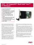
F19P – 3U CompactPCI®
PlusIO Intel® Core™ 2
Duo CPU Board
F19P - 3U CompactPCI® PlusIO Intel® Core™ 2 Duo CPU Board
F19P - 3U CompactPCI® PlusIO Intel® Core™ 2 Duo CPU
Board
The F19P versatile 4HP/3U single-board computer is a continuation of MEN's
proven range of Intel® CPU boards. It is equipped with the Intel® Core 2 Duo
processor SP9300 running at 2.26 GHz and offering multi-core processor
architecture from Intel® with full 64-bit support. The CPU card delivers an
excellent graphics performance and is designed especially for embedded systems
which require high computing performance with low power consumption.
The F19P offers a 32-bit/33-MHz CompactPCI® bus interface and can also be used
without a bus system. It offers 4 USB 2.0 and 4 fast (3Gb/s) SATA interfaces as well
as 4 PCI Express® x1 links and one Gigabit Ethernet on the J2 rear I/O connector
which is compatible with the PICMG 2.30 CompactPCI® PlusIO specification.
A total of seven PCI Express® lanes for high-speed communication (such as
Gigabit Ethernet) are supported on the F19P. 3 x1 PCIe® links are used for the three
onboard Ethernet interfaces. 4 x1 PCIe® links are available via rear I/O or on a
specific side card.
The F19P is equipped with DDR3 DRAM which is soldered to the F19P to
guarantee optimum shock and vibration resistance. A robust CompactFlash® and
microSD™ card device which are connected via a USB interface offer nearly
unlimited space for user applications.
The standard I/O available at the front panel of F19P includes graphics on a VGA
connector, two PCIe®-driven Gigabit Ethernet as well as two USB 2.0 ports.
The F19P can be extended by different side cards. Additional functions include two
digital video interfaces for flat panel connection via DVI (multimedia), a variety of
different UARTs or another four USBs, SATA for hard disk connection and HD
audio.
Thermal supervision of the processor and a watchdog for the operating system
complete the functionality of the F19P.
The F19P operates in Windows® and Linux environments as well as under real-time
operating systems that support Intel®'s multi-core architecture. The InsydeH2O™
EFI BIOS was specially designed for embedded system applications.
Equipped with Intel® components exclusively from the Intel® Embedded Line, the
F19P has a guaranteed minimum standard availability of 7 years.
The F19P is suited for a wide range of industrial applications, e.g. for monitoring,
vision and control systems as well as test and measurement.
The F19P comes with a tailored passive heat sink within 4 HP height. The robust
design of the F19P make the board especially suited for use in rugged environments
with regard to shock and vibration according to applicable DIN, EN or IEC industry
standards. The F19P is also ready for coating so that it can be used in humid and
dusty environments.
MEN Mikro Elektronik GmbH
20F019P00 E6 – 2015-01-13
2
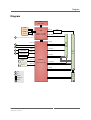
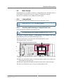
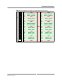
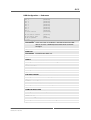
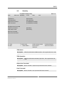
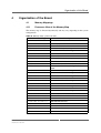
Diagram
Diagram
Intel®
Core™ 2 Duo
DDR3
SDRAM
GS45
DDR3
SDRAM
Memory Controller
Graphics Controller
PCIe x1
Ethernet
10/100/1000Base-T
Dual SDVO
VGA
F
USB 2.0
USB 2.0
F
USB 2.0
F
F
Ethernet
10/100/1000Base-T
F
Ethernet
10/100/1000Base-T
SideCard
Connector
HD Audio
PCIe x1
J2
Rear
I/O
PCIe x1
4 PCIe x1
B
Watchdog
B
Compact
Flash
USB 2.0
ICH9M-SFF
I/O Controller Hub
SATA (3Gb)
USB 2.0
B
MicroSD
USB 2.0
R
F Front
R Rear
B Onboard
SA SA-Adapter™
Options
MEN Mikro Elektronik GmbH
20F019P00 E6 – 2015-01-13
PCI
J1 cPCI
or:
Busless
+5V
R
3
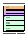
Technical Data
Technical Data
CPU
• Intel® Core™ 2 Duo SP9300
- Up to 2.26 GHz processor core frequency
- 1066 MHz system bus frequency
• Chipset
- Northbridge: Intel® GS45
- Southbridge: Intel® ICH9M-SFF
Memory
• Up to 6 MB L2 cache integrated in Core 2 Duo
• Up to 4 GB DDR3 SDRAM system memory
- Soldered
- 800/1067 MHz memory bus frequency locked to the FSB frequency
• 16 Mbits boot Flash
• Serial EEPROM 2kbits for factory settings
• CompactFlash® card interface
- Via USB
- Type I
- True IDE
- DMA support
• MicroSD card interface
- Via USB
Mass Storage
• CompactFlash®
- Connected via USB
• MicroSD card
- Connected via USB
• Serial ATA (SATA)
- Four channels via rear I/O, one channel via side-card connector (switchable)
- Transfer rates up to 3 Gbit/s
- RAID level 0/1 support
Graphics
• Integrated in GS45 chipset
- Up to 533 MHz graphics core
- Maximum resolution: 2048 x 1536 pixels
• VGA connector at front panel
• Two SDVO ports available via side-card connector
- Two additional DVI connectors at front panel optional via side card
- Simultaneous connection of two monitors
MEN Mikro Elektronik GmbH
20F019P00 E6 – 2015-01-13
4
Technical Data
I/O
• USB
- Two USB 2.0 ports via Series A connectors at front panel
- Four USB 2.0 ports via side-card connector
- Four USB 2.0 ports via rear I/O
- One USB for connection of CompactFlash®/MicroSD or USB NAND Flash
- UHCI implementation
- Data rates up to 480Mbit/s
• Ethernet
- Two 10/100/1000Base-T Ethernet channels at the front
- RJ45 connectors at front panel
- Ethernet controllers are connected by two x1 PCIe® links from ICH9M
- Onboard LEDs to signal activity status and connection speed
- One 10/100/1000Base-T Ethernet channel via rear I/O
- Ethernet controller is connected by one x1 PCIe® link from GS45
• High Definition (HD) audio
- Accessible via side-card connector
Front Connections (Standard)
• VGA
• Two USB 2.0 (Series A)
• Two Ethernet (RJ45)
Rear I/O
•
•
•
•
•
Four SATA
Four USB
One Gigabit Ethernet
Four PCI Express® x1 links
Compatible with PICMG 2.30 CompactPCI® PlusIO
- 1PCI33/4PCIE2.5/4SATA3/4USB2/1ETH1G
Miscellaneous
• Board controller
• Real-time clock, buffered by a GoldCap or alternatively a battery (5 years life
cycle)
• Watchdog timer
• Temperature measurement
• One user LED
• Reset button
PCI Express®
• Three x1 links to connect local 1000Base-T Ethernet controllers
- Data rate 250 MB/s in each direction (2.5 Gbit/s per lane)
• Four x1 links for extension through side-card connector or rear I/O
- Data rate up to 1 GB/s in each direction (2.5 Gbit/s per lane)
MEN Mikro Elektronik GmbH
20F019P00 E6 – 2015-01-13
5
Technical Data
CompactPCI® Bus
•
•
•
•
Compliance with CompactPCI® Core Specification PICMG 2.0 R3.0
System slot
32-bit/33-MHz CompactPCI® bus
V(I/O): +3.3 V (+5 V tolerant)
Busless Operation
• Board can be supplied with +5 V only, all other voltages are generated on the
board
• Backplane connectors used only for power supply
Electrical Specifications
• Supply voltage/power consumption with Celeron® M722 processor:
- +5 V (-3%/+5%), 2.2 A typ., 2.7 A max.
- +3.3 V (-3%/+5%), 1.4 A (2 Gb Ethernet), 1 A (1 Gb Ethernet)
- +12 V (-10%/+10%), approx. 10 mA
- If the board is supplied with 5 V only (typically without a bus connection),
the 3.3 V are generated on the board and fed to the backplane (3 A max.)
• Supply voltage/power consumption with SP9300 processor:
- +5 V (-3%/+5%), 4.9 A typ., 6.4 A max.
- +3.3 V (-3%/+5%), 1.4 A (2 Gb Ethernet), 1 A (1 Gb Ethernet)
- +12 V (-10%/+10%), approx. 10 mA
- If the board is supplied with 5 V only (typically without a bus connection),
the 3.3 V are generated on the board and fed to the backplane (3 A max.)
Mechanical Specifications
• Dimensions: conforming to CompactPCI® specification for 3U boards
• Front panel: 4HP with ejector
• Weight: 430 g
Environmental Specifications
• Temperature range (operation):
- Depends on system configuration (CPU, hard disk, heat sink...)
- Maximum: +85°C
- Minimum: -40°C (all processors)
- Conditions: airflow 1.5 m/s, typical power dissipation: 9.8 W (F19P version
with Celeron® M722), 13.4 W (F19P version with SP9300 Core 2 Duo) with
Windows® XP operating system and 1 Gb Ethernet connection
• Temperature range (storage): -40..+85°C
• Relative humidity (operation): max. 95% non-condensing
• Relative humidity (storage): max. 95% non-condensing
• Altitude: -300 m to +2,000 m
• Shock: 50 m/s², 30 ms
• Vibration (function): 1 m/s², 5 Hz – 150 Hz
• Vibration (lifetime): 7.9 m/s², 5 Hz – 150 Hz
• Conformal coating on request
MEN Mikro Elektronik GmbH
20F019P00 E6 – 2015-01-13
6
Technical Data
MTBF
• 552,030h @ 40°C according to IEC/TR 62380 (RDF2000)
Safety
• PCB manufactured with a flammability rating of 94V-0 by UL recognized
manufacturers
EMC
• Tested according to EN 55022 (radio disturbance), IEC 61000-4-3
(electromagnetic field immunity), IEC 61000-4-4 (burst), IEC 61000-4-5 (surge)
and IEC 61000-4-6 (conducted disturbances)
BIOS
• InsydeH2O™ UEFI Framework
Software Support
• Note that 64-bit hardware technology can be used in an optimal way with 64-bit
operating system support
• Windows® (Windows® XP, Windows® 7)
• Linux
- tested/verified with: Ubuntu 10.04 (kernel 2.6.32-21) 32-bit and 64-bit
versions
- OpenSuse 11.3 32-bit and 64-bit versions
- and: CentOS 5.5 (kernel 2.6.18) 32-bit and 64-bit versions
- Detailed matrix of supported interfaces under Ubuntu 10.04 and OpenSuse
11.3
• VxWorks®
• QNX®
• Intel® Virtualization Technology, allows a platform to run multiple operating
systems and applications in independent partitions; one computer system can
function as multiple virtual systems
For more information on supported operating system versions and
drivers see online data sheet.
MEN Mikro Elektronik GmbH
20F019P00 E6 – 2015-01-13
7
Configuration Options
Configuration Options
CPU
•
•
•
•
•
Intel® SP9300, 2.26 GHz, 1066 MHz FSB, 6 MB cache, 25 W
Intel® SL9400, 1.86 GHz, 1066 MHz FSB, 6 MB cache, 17 W
Intel® SU9300, 1.2 GHz, 800 MHz FSB, 3 MB cache, 10 W
Intel® Celeron® M722, 1.2 GHz, 800 MHz FSB, 1 MB cache, 5.5 W
Intel® Celeron® M723, 1.2 GHz, 800 MHz FSB, 1 MB cache, 10 W
Memory
• System RAM
- 2 GB or 4 GB
• CompactFlash®
- 0 MB up to maximum available
• MicroSD card
- 0 MB up to maximum available
• NAND Flash instead of CompactFlash®, microSD™ card and battery
- 0 MB up to maximum available
Graphics
• One or two DVI-D connectors at front via side card
- Simultaneous connection of two monitors
I/O
• Ethernet
- 9-pin D-Sub connector with one or two 10/100Base-T ports instead of two
RJ45 connectors
- Two M12 connectors with two 10/100/1000Base-T ports on 8HP instead of
two RJ45 connectors
Mechanical
• Side card can be added at left or right side of CPU
• Adapter board for two M12 Ethernet connectors can be added at left or right side
of CPU
MEN Mikro Elektronik GmbH
20F019P00 E6 – 2015-01-13
8
Configuration Options
Operation Temperature
• Depends on system configuration (CPU, hard disk, heat sink...)
• Maximum: +85°C
• Minimum: -40°C (all processors)
Cooling Concept
• Also available with conduction cooling in MEN CCA frame
Please note that some of these options may only be available for large volumes.
For available standard configurations see the F19P online data sheet.
Please contact MEN’s sales team for further information.
MEN Mikro Elektronik GmbH
20F019P00 E6 – 2015-01-13
9
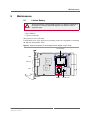
Product Safety
Product Safety
Lithium Battery
!
This board contains a lithium battery. There is a danger of explosion if
the battery is incorrectly replaced! For replacing the battery correctly
see Chapter 5 Maintenance on page 90.
Electrostatic Discharge (ESD)
!
MEN Mikro Elektronik GmbH
20F019P00 E6 – 2015-01-13
Computer boards and components contain electrostatic sensitive
devices. Electrostatic discharge (ESD) can damage components. To
protect the board and other components against damage from static
electricity, you should follow some precautions whenever you work on
your computer.
• Power down and unplug your computer system when working on the
inside.
• Hold components by the edges and try not to touch the IC chips,
leads, or circuitry.
• Use a grounded wrist strap before handling computer components.
• Place components on a grounded antistatic pad or on the bag that
came with the component whenever the components are separated
from the system.
Store the board only in its original ESD-protected packaging. Retain
the original packaging in case you need to return the board to MEN for
repair.
10
About this Document
About this Document
This user manual is intended only for system developers and integrators, it is not
intended for end users.
It describes the hardware functions of the board, connection of peripheral devices
and integration into a system. It also provides additional information for special
applications and configurations of the board.
The manual does not include detailed information on individual components (data
sheets etc.). A list of literature is given in the appendix.
History
Issue
Date
E1
First issue
2009-09-30
E2
General update, corrected MAC addresses and
Ethernet LED behavior
2010-08-24
E3
Updated BIOS description (see Chapter 3 BIOS)
2011-03-04
E4
Added Chapter 1.6.2 Installing Windows XP or
Windows 7 on USB Devices, modified Chapter 2.1
Power Supply, added M12 Ethernet option,
structured Chapter 2.11 Ethernet Interfaces more
logically
2011-09-19
E5
Deleted 1x4 PCIe link (not supported)
2012-01-25
E6
Cosmetics, corrected options, added RTC
accuracy, reworked block diagram
2015-01-13
MEN Mikro Elektronik GmbH
20F019P00 E6 – 2015-01-13
Comments
11
About this Document
Conventions
!
italics
bold
monospace
This sign marks important notes or warnings concerning proper functionality of the
product described in this document. You should read them in any case.
Folder, file and function names are printed in italics.
Bold type is used for emphasis.
A monospaced font type is used for hexadecimal numbers, listings, C function
descriptions or wherever appropriate. Hexadecimal numbers are preceded by "0x".
comment
Comments embedded into coding examples are shown in green color.
hyperlink
Hyperlinks are printed in blue color.
The globe will show you where hyperlinks lead directly to the Internet, so you can
look for the latest information online.
IRQ#
/IRQ
Signal names followed by "#" or preceded by a slash ("/") indicate that this signal is
either active low or that it becomes active at a falling edge.
in/out
Signal directions in signal mnemonics tables generally refer to the corresponding
board or component, "in" meaning "to the board or component", "out" meaning
"coming from it".
Vertical lines on the outer margin signal technical changes to the previous issue of
the document.
MEN Mikro Elektronik GmbH
20F019P00 E6 – 2015-01-13
12
About this Document
Legal Information
Changes
MEN Mikro Elektronik GmbH ("MEN") reserves the right to make changes without further notice to any products
herein.
Warranty, Guarantee, Liability
MEN makes no warranty, representation or guarantee of any kind regarding the suitability of its products for any
particular purpose, nor does MEN assume any liability arising out of the application or use of any product or
circuit, and specifically disclaims any and all liability, including, without limitation, consequential or incidental
damages. TO THE EXTENT APPLICABLE, SPECIFICALLY EXCLUDED ARE ANY IMPLIED
WARRANTIES ARISING BY OPERATION OF LAW, CUSTOM OR USAGE, INCLUDING WITHOUT
LIMITATION, THE IMPLIED WARRANTIES OF MERCHANTABILITY AND FITNESS FOR A
PARTICULAR PURPOSE OR USE. In no event shall MEN be liable for more than the contract price for the
products in question. If buyer does not notify MEN in writing within the foregoing warranty period, MEN shall
have no liability or obligation to buyer hereunder.
The publication is provided on the terms and understanding that:
1. MEN is not responsible for the results of any actions taken on the basis of information in the publication, nor
for any error in or omission from the publication; and
2. MEN is not engaged in rendering technical or other advice or services.
MEN expressly disclaims all and any liability and responsibility to any person, whether a reader of the publication
or not, in respect of anything, and of the consequences of anything, done or omitted to be done by any such person
in reliance, whether wholly or partially, on the whole or any part of the contents of the publication.
Conditions for Use, Field of Application
The correct function of MEN products in mission-critical and life-critical applications is limited to the
environmental specification given for each product in the technical user manual. The correct function of MEN
products under extended environmental conditions is limited to the individual requirement specification and
subsequent validation documents for each product for the applicable use case and has to be agreed upon in writing
by MEN and the customer. Should the customer purchase or use MEN products for any unintended or
unauthorized application, the customer shall indemnify and hold MEN and its officers, employees, subsidiaries,
affiliates, and distributors harmless against all claims, costs, damages, and expenses, and reasonable attorney fees
arising out of, directly or indirectly, any claim or personal injury or death associated with such unintended or
unauthorized use, even if such claim alleges that MEN was negligent regarding the design or manufacture of the
part. In no case is MEN liable for the correct function of the technical installation where MEN products are a part
of.
Trademarks
All products or services mentioned in this publication are identified by the trademarks, service marks, or product
names as designated by the companies which market those products. The trademarks and registered trademarks
are held by the companies producing them. Inquiries concerning such trademarks should be made directly to those
companies.
Conformity
MEN products are no ready-made products for end users. They are tested according to the standards given in the
Technical Data and thus enable you to achieve certification of the product according to the standards applicable in
your field of application.
MEN Mikro Elektronik GmbH
20F019P00 E6 – 2015-01-13
13
About this Document
RoHS
Since July 1, 2006 all MEN standard products comply with RoHS legislation.
Since January 2005 the SMD and manual soldering processes at MEN have already been completely lead-free.
Between June 2004 and June 30, 2006 MEN’s selected component suppliers have changed delivery to RoHScompliant parts. During this period any change and status was traceable through the MEN ERP system and the
boards gradually became RoHS-compliant.
WEEE Application
The WEEE directive does not apply to fixed industrial plants and tools. The compliance is the responsibility of the
company which puts the product on the market, as defined in the directive; components and sub-assemblies are
not subject to product compliance.
In other words: Since MEN does not deliver ready-made products to end users, the WEEE directive is not
applicable for MEN. Users are nevertheless recommended to properly recycle all electronic boards which have
passed their life cycle.
Nevertheless, MEN is registered as a manufacturer in Germany. The registration number can be provided on
request.
Copyright © 2014 MEN Mikro Elektronik GmbH. All rights reserved.
Germany
MEN Mikro Elektronik GmbH
Neuwieder Straße 3-7
90411 Nuremberg
Phone +49-911-99 33 5-0
Fax +49-911-99 33 5-901
E-mail [email protected]
www.men.de
MEN Mikro Elektronik GmbH
20F019P00 E6 – 2015-01-13
France
MEN Mikro Elektronik SAS
18, rue René Cassin
ZA de la Châtelaine
74240 Gaillard
Phone +33 (0) 450-955-312
Fax +33 (0) 450-955-211
E-mail [email protected]
www.men-france.fr
USA
MEN Micro Inc.
860 Penllyn Blue Bell Pike
Blue Bell, PA 19422
Phone (215) 542-9575
Fax (215) 542-9577
E-mail [email protected]
www.menmicro.com
14
Contents
Contents
1 Getting Started . . . . . . . . . . . . . . . . . . . . . . . . . . . . . . . . . . . . . . . . . . . . . . . .
1.1 Map of the Board. . . . . . . . . . . . . . . . . . . . . . . . . . . . . . . . . . . . . . . . .
1.2 Configuring the Hardware . . . . . . . . . . . . . . . . . . . . . . . . . . . . . . . . . .
1.3 Integrating the Board into a System . . . . . . . . . . . . . . . . . . . . . . . . . .
1.4 Troubleshooting at Start-up . . . . . . . . . . . . . . . . . . . . . . . . . . . . . . . . .
1.5 Configuring BIOS . . . . . . . . . . . . . . . . . . . . . . . . . . . . . . . . . . . . . . . .
1.6 Installing Operating System Software. . . . . . . . . . . . . . . . . . . . . . . . .
1.6.1
Installing Windows 2000 via USB . . . . . . . . . . . . . . . . . . . .
1.6.2
Installing Windows XP or Windows 7 on USB Devices . . .
1.7 Installing Driver Software . . . . . . . . . . . . . . . . . . . . . . . . . . . . . . . . . .
19
19
21
22
23
23
23
23
23
23
2 Functional Description . . . . . . . . . . . . . . . . . . . . . . . . . . . . . . . . . . . . . . . . . .
2.1 Power Supply. . . . . . . . . . . . . . . . . . . . . . . . . . . . . . . . . . . . . . . . . . . .
2.2 Board Supervision . . . . . . . . . . . . . . . . . . . . . . . . . . . . . . . . . . . . . . . .
2.3 Reset and Power-Off Behavior . . . . . . . . . . . . . . . . . . . . . . . . . . . . . .
2.4 Real-Time Clock . . . . . . . . . . . . . . . . . . . . . . . . . . . . . . . . . . . . . . . . .
2.5 Processor Core. . . . . . . . . . . . . . . . . . . . . . . . . . . . . . . . . . . . . . . . . . .
2.5.1
Thermal Considerations . . . . . . . . . . . . . . . . . . . . . . . . . . . .
2.6 Bus Structure . . . . . . . . . . . . . . . . . . . . . . . . . . . . . . . . . . . . . . . . . . . .
2.7 Memory . . . . . . . . . . . . . . . . . . . . . . . . . . . . . . . . . . . . . . . . . . . . . . . .
2.7.1
DRAM System Memory . . . . . . . . . . . . . . . . . . . . . . . . . . . .
2.7.2
Boot Flash . . . . . . . . . . . . . . . . . . . . . . . . . . . . . . . . . . . . . . .
2.8 Mass Storage . . . . . . . . . . . . . . . . . . . . . . . . . . . . . . . . . . . . . . . . . . . .
2.8.1
CompactFlash . . . . . . . . . . . . . . . . . . . . . . . . . . . . . . . . . . . .
2.8.2
MicroSD Card . . . . . . . . . . . . . . . . . . . . . . . . . . . . . . . . . . . .
2.8.3
Optional USB SSD . . . . . . . . . . . . . . . . . . . . . . . . . . . . . . . .
2.8.4
Serial ATA (SATA) . . . . . . . . . . . . . . . . . . . . . . . . . . . . . . . .
2.9 Graphics. . . . . . . . . . . . . . . . . . . . . . . . . . . . . . . . . . . . . . . . . . . . . . . .
2.9.1
Connection via VGA. . . . . . . . . . . . . . . . . . . . . . . . . . . . . . .
2.9.2
Connection via SDVO. . . . . . . . . . . . . . . . . . . . . . . . . . . . . .
2.10 USB Interfaces. . . . . . . . . . . . . . . . . . . . . . . . . . . . . . . . . . . . . . . . . . .
2.10.1 Front-Panel Connection . . . . . . . . . . . . . . . . . . . . . . . . . . . .
2.10.2 Side-Card Connection . . . . . . . . . . . . . . . . . . . . . . . . . . . . . .
2.10.3 Rear I/O Connection (CompactPCI PlusIO) . . . . . . . . . . . . .
2.11 Ethernet Interfaces. . . . . . . . . . . . . . . . . . . . . . . . . . . . . . . . . . . . . . . .
2.11.1 Front-Panel Connection . . . . . . . . . . . . . . . . . . . . . . . . . . . .
2.11.2 Rear I/O Connection . . . . . . . . . . . . . . . . . . . . . . . . . . . . . . .
2.12 High Definition (HD) Audio Interface . . . . . . . . . . . . . . . . . . . . . . . .
2.13 Side-Card Interface . . . . . . . . . . . . . . . . . . . . . . . . . . . . . . . . . . . . . . .
2.13.1 Connection . . . . . . . . . . . . . . . . . . . . . . . . . . . . . . . . . . . . . .
2.13.2 Installing a Side Card . . . . . . . . . . . . . . . . . . . . . . . . . . . . . .
2.14 PCI Express . . . . . . . . . . . . . . . . . . . . . . . . . . . . . . . . . . . . . . . . . . . . .
24
24
25
26
26
26
27
27
27
27
27
28
28
29
29
29
30
30
30
31
31
31
32
33
34
35
36
36
37
43
46
MEN Mikro Elektronik GmbH
20F019P00 E6 – 2015-01-13
15
Contents
2.14.1 General . . . . . . . . . . . . . . . . . . . . . . . . . . . . . . . . . . . . . . . . .
2.14.2 Implementation on F19P . . . . . . . . . . . . . . . . . . . . . . . . . . . .
2.15 CompactPCI Interface . . . . . . . . . . . . . . . . . . . . . . . . . . . . . . . . . . . . .
2.15.1 General . . . . . . . . . . . . . . . . . . . . . . . . . . . . . . . . . . . . . . . . .
2.15.2 CompactPCI PlusIO Rear I/O . . . . . . . . . . . . . . . . . . . . . . . .
2.16 Reset Button and Status LED . . . . . . . . . . . . . . . . . . . . . . . . . . . . . . .
46
46
47
47
47
51
3 BIOS . . . . . . . . . . . . . . . . . . . . . . . . . . . . . . . . . . . . . . . . . . . . . . . . . . . . . . . . .
3.1 Main. . . . . . . . . . . . . . . . . . . . . . . . . . . . . . . . . . . . . . . . . . . . . . . . . . .
3.2 Advanced . . . . . . . . . . . . . . . . . . . . . . . . . . . . . . . . . . . . . . . . . . . . . . .
3.3 Security . . . . . . . . . . . . . . . . . . . . . . . . . . . . . . . . . . . . . . . . . . . . . . . .
3.4 Power . . . . . . . . . . . . . . . . . . . . . . . . . . . . . . . . . . . . . . . . . . . . . . . . . .
3.5 Boot . . . . . . . . . . . . . . . . . . . . . . . . . . . . . . . . . . . . . . . . . . . . . . . . . . .
3.6 Exit . . . . . . . . . . . . . . . . . . . . . . . . . . . . . . . . . . . . . . . . . . . . . . . . . . .
3.6.1
Exit Saving Changes . . . . . . . . . . . . . . . . . . . . . . . . . . . . . . .
3.6.2
Save Change Without Exit . . . . . . . . . . . . . . . . . . . . . . . . . .
3.6.3
Exit Discarding Changes. . . . . . . . . . . . . . . . . . . . . . . . . . . .
3.6.4
Load Optimal Defaults . . . . . . . . . . . . . . . . . . . . . . . . . . . . .
3.6.5
Load Custom Defaults. . . . . . . . . . . . . . . . . . . . . . . . . . . . . .
3.6.6
Save Custom Defaults . . . . . . . . . . . . . . . . . . . . . . . . . . . . . .
3.6.7
Discard Changes . . . . . . . . . . . . . . . . . . . . . . . . . . . . . . . . . .
52
53
55
70
72
78
81
81
81
81
81
82
82
82
4 Organization of the Board . . . . . . . . . . . . . . . . . . . . . . . . . . . . . . . . . . . . . . .
4.1 Memory Mappings . . . . . . . . . . . . . . . . . . . . . . . . . . . . . . . . . . . . . . .
4.1.1
Processor View of the Memory Map. . . . . . . . . . . . . . . . . . .
4.1.2
I/O Memory Map . . . . . . . . . . . . . . . . . . . . . . . . . . . . . . . . .
4.2 PCI Devices . . . . . . . . . . . . . . . . . . . . . . . . . . . . . . . . . . . . . . . . . . . . .
4.3 SMBus Devices . . . . . . . . . . . . . . . . . . . . . . . . . . . . . . . . . . . . . . . . . .
4.4 Interrupt Mapping . . . . . . . . . . . . . . . . . . . . . . . . . . . . . . . . . . . . . . . .
83
83
83
84
87
88
88
5 Maintenance . . . . . . . . . . . . . . . . . . . . . . . . . . . . . . . . . . . . . . . . . . . . . . . . . . 90
5.1 Lithium Battery . . . . . . . . . . . . . . . . . . . . . . . . . . . . . . . . . . . . . . . . . . 90
6 Appendix . . . . . . . . . . . . . . . . . . . . . . . . . . . . . . . . . . . . . . . . . . . . . . . . . . . . .
6.1 Literature and Web Resources . . . . . . . . . . . . . . . . . . . . . . . . . . . . . . .
6.1.1
CPU . . . . . . . . . . . . . . . . . . . . . . . . . . . . . . . . . . . . . . . . . . . .
6.1.2
IDE . . . . . . . . . . . . . . . . . . . . . . . . . . . . . . . . . . . . . . . . . . . .
6.1.3
SATA . . . . . . . . . . . . . . . . . . . . . . . . . . . . . . . . . . . . . . . . . . .
6.1.4
USB . . . . . . . . . . . . . . . . . . . . . . . . . . . . . . . . . . . . . . . . . . . .
6.1.5
Ethernet . . . . . . . . . . . . . . . . . . . . . . . . . . . . . . . . . . . . . . . . .
6.1.6
HD Audio . . . . . . . . . . . . . . . . . . . . . . . . . . . . . . . . . . . . . . .
6.1.7
PCI Express. . . . . . . . . . . . . . . . . . . . . . . . . . . . . . . . . . . . . .
6.1.8
CompactPCI/PCI. . . . . . . . . . . . . . . . . . . . . . . . . . . . . . . . . .
6.1.9
CompactPCI PlusIO . . . . . . . . . . . . . . . . . . . . . . . . . . . . . . .
6.2 Finding out the Board’s Article Number, Revision
and Serial Number . . . . . . . . . . . . . . . . . . . . . . . . . . . . . . . . . . . . . . . .
MEN Mikro Elektronik GmbH
20F019P00 E6 – 2015-01-13
91
91
91
91
91
91
91
92
92
92
92
93
16
Figures
Figure 1.
Figure 2.
Figure 3.
Figure 4.
MEN Mikro Elektronik GmbH
20F019P00 E6 – 2015-01-13
Map of the board – front view . . . . . . . . . . . . . . . . . . . . . . . . . . . . . . .
Map of the board – top view. . . . . . . . . . . . . . . . . . . . . . . . . . . . . . . . .
Position of battery on the CompactFlash adapter on the F19P. . . . . . .
Labels giving the board’s article number, revision and
serial number . . . . . . . . . . . . . . . . . . . . . . . . . . . . . . . . . . . . . . . . . . . .
19
20
90
93
17
Tables
Table 1.
Table 2.
Table 3.
Table 4.
Table 5.
Table 6.
Table 7.
Table 8.
Table 9.
Table 10.
Table 11.
Table 12.
Table 13.
Table 14.
Table 15.
Table 16.
Table 17.
Table 18.
Table 19.
Table 20.
MEN Mikro Elektronik GmbH
20F019P00 E6 – 2015-01-13
Processor core options on F19P . . . . . . . . . . . . . . . . . . . . . . . . . . . . . .
Pin assignment of 15-pin HD-Sub VGA receptacle connector . . . . . .
Signal mnemonics of 15-pin HD-Sub VGA connector . . . . . . . . . . . .
Pin assignment of USB front-panel connectors . . . . . . . . . . . . . . . . . .
Signal mnemonics of USB front-panel connectors . . . . . . . . . . . . . . .
Signal mnemonics of Ethernet 10/100/1000Base-T connectors. . . . . .
Pin assignment and status LEDs of 8-pin RJ45 Ethernet
10/100/1000Base-T connectors (LAN1/LAN2). . . . . . . . . . . . . . . . . .
Pin assignment of 9-pin D-Sub 10Base-T/100Base-TX
plug connector (LAN1/LAN2) . . . . . . . . . . . . . . . . . . . . . . . . . . . . . . .
Pin assignment of 114-pin side-card connector, pins 1..38 . . . . . . . . .
Pin assignment of 114-pin side-card connector, pins 39..76 . . . . . . . .
Pin assignment of 114-pin side-card connector, pins 77..114 . . . . . . .
Signal mnemonics of 114-pin side-card connector . . . . . . . . . . . . . . .
Pin assignment of CompactPCI connector J2. . . . . . . . . . . . . . . . . . . .
Signal mnemonics of CompactPCI connector J2 – CompactPCI
and CompactPCI PlusIO rear I/O . . . . . . . . . . . . . . . . . . . . . . . . . . . . .
Error codes signaled by board management controller via
LED flashes . . . . . . . . . . . . . . . . . . . . . . . . . . . . . . . . . . . . . . . . . . . . .
Memory map – processor view . . . . . . . . . . . . . . . . . . . . . . . . . . . . . .
Memory map - I/O . . . . . . . . . . . . . . . . . . . . . . . . . . . . . . . . . . . . . . . .
PCI Devices . . . . . . . . . . . . . . . . . . . . . . . . . . . . . . . . . . . . . . . . . . . . .
SMBus devices . . . . . . . . . . . . . . . . . . . . . . . . . . . . . . . . . . . . . . . . . . .
Interrupt Mapping. . . . . . . . . . . . . . . . . . . . . . . . . . . . . . . . . . . . . . . . .
26
30
30
31
31
34
34
35
37
38
39
40
48
49
51
83
84
87
88
88
18
Getting Started
1
Getting Started
This chapter gives an overview of the board and some hints for first installation in a
system.
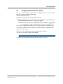
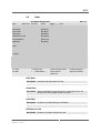
1.1
Map of the Board
Figure 1. Map of the board – front view
F19P Standard
Side Card
®
RST
STA
1
2 3
4
VGA
F19P
MEN Mikro Elektronik GmbH
20F019P00 E6 – 2015-01-13
19
Getting Started
Figure 2. Map of the board – top view
CompactFlash
USB
Ethernet
VGA
Battery
MEN Mikro Elektronik GmbH
20F019P00 E6 – 2015-01-13
microSD Card
20
Getting Started
1.2
Configuring the Hardware
You should check your hardware requirements before installing the board in a
system, since most modifications are difficult or even impossible to do when the
board is mounted in a system.
The following check list gives an overview on what you might want to configure.
CompactFlash
The board is shipped without a CompactFlash card. You should check your
needs and install a suitable CompactFlash card.
Refer to Chapter 2.8.1.1 Inserting and Extracting a CompactFlash Card on
page 28 for details on the IDE interface.
microSD
The board is shipped without a microSD card. You should check your needs
and install a suitable microSD card.
Refer to Chapter 2.8.2 MicroSD Card on page 29
Expansion by a side card
The board offers the option of adding one side card. Side cards come in
standard 3U format and can be attached directly to F19P at the heat sink side.
Every side card has dedicated functions, e.g. legacy COM interfaces, SATA
hard disk or DVI front connectors.
See Chapter 2.13 Side-Card Interface on page 36 for details on side cards.
The MEN sales staff will be glad to help you find the right extension
and front panel solution. See also MEN’s website for ordering
information and standard products.
MEN Mikro Elektronik GmbH
20F019P00 E6 – 2015-01-13
21
Getting Started
1.3
Integrating the Board into a System
You can use the following check list when installing the F19P in a system for the
first time and with minimum configuration.
Power-down the system.
Remove all boards from the CompactPCI system.
Insert the F19P into the system slot of your CompactPCI system, making sure
that the CompactPCI connectors are properly aligned.
Note: The system slot of every CompactPCI system is marked by a
triangle
on the backplane and/or at the front panel. It also has red guide rails.
Connect a USB keyboard and mouse to the USB connectors at the front panel.
Connect a CRT or flat-panel display to the VGA connector at the front panel.
Power-up the system.
You can start up the BIOS setup menu by hitting the <F2> key.
Now you can make configurations in BIOS.
For more information on the BIOS see Chapter 3 BIOS on page 52.
Observe the installation instructions for the respective software.
MEN Mikro Elektronik GmbH
20F019P00 E6 – 2015-01-13
22
Getting Started
1.4
Troubleshooting at Start-up
If you have any problems at start-up of the F19P, you can start the board with EFI
default settings for troubleshooting.
For more information on the BIOS see Chapter 3 BIOS on page 52.
1.5
Configuring BIOS
The F19P is equipped with an InsydeH2O UEFI framework. Normally you won’t
need to make any changes in the BIOS setup.
For more information on the BIOS see Chapter 3 BIOS on page 52.
1.6
Installing Operating System Software
The board supports Windows, Linux, VxWorks and QNX.
!
1.6.1
By standard, no operating system is installed on the board. Please
refer to the respective manufacturer's documentation on how to install
operating system software!
Installing Windows 2000 via USB
If you want to install Windows 2000 using a USB CD-ROM drive, you must install
from a Windows 2000 CD including Service Pack 4 to avoid problems. This is a
known Windows problem.
1.6.2
Installing Windows XP or Windows 7 on USB Devices
The CompactFlash and the microSD card of the F19P are connected via USB. A
standard Windows operating system (like Windows XP Professional or Windows 7
Ultimate) does not support direct installation on USB memory devices.
There are two possible solutions:
• Add a hard drive (SATA, mSATA) on a peripheral board or side card
• Switch to an Embedded Windows (like Windows Embedded Standard or Windows Embedded Standard 7). These Embedded Windows operating systems support being installed on and booted from a USB device.
Linux supports booting from a USB device without problems.
1.7
Installing Driver Software
For a detailed description on how to install driver software please refer to the
respective documentation.
You can find any driver software and documentation for the F19P
available for download on MEN’s website.
MEN Mikro Elektronik GmbH
20F019P00 E6 – 2015-01-13
23
Functional Description
2
Functional Description
The following describes the individual functions of the board and their
configuration on the board. There is no detailed description of the individual
controller chips and the CPU. They can be obtained from the data sheets or data
books of the semiconductor manufacturer concerned.
For more information, see Chapter 6.1 Literature and Web Resources on page 91.
2.1
Power Supply
There are only two possible ways to power the F19P:
• +5V, +3.3V and +12V via CompactPCI connector J1
• +5V only via CompactPCI connector J1
!
MEN Mikro Elektronik GmbH
20F019P00 E6 – 2015-01-13
To supply the board with 3.3V and 5V is not allowed and may cause
serious damage. If +3.3V are supplied via CompactPCI connector J1,
the +12V supply always has to be present.
If the +12V are not present, the board automatically generates +3.3V
and also feeds them to the backplane, which would cause a conflict
with the external +3.3V supply.
24
Functional Description
2.2
Board Supervision
The F19P provides an intelligent board management controller (BMC) with the
following main features:
•
•
•
•
•
•
•
Board power sequencing control
Voltage supervision
System watchdog
Software reset functionality
Error state logging
Power mode settings
SMBus communication with main CPU
The watchdog device monitors the board on operating system level. If enabled, the
watchdog must be triggered by application software. If the trigger is overdue, the
watchdog initiates a board reset and this way can put the system back into operation
when the software hangs.
The watchdog uses a configurable time interval or is disabled. Settings are made
through BIOS or via an MEN software driver.
In addition, the F19P uses a National LM95245 device to measure the CPU die
temperature and the local board temperature.
MEN provides dedicated software drivers for the board controller and LM95245
device. For a detailed description of the functionality of the driver software please
refer to the drivers’ documentation.
You can find any driver software and documentation available for
download on MEN’s website.
MEN Mikro Elektronik GmbH
20F019P00 E6 – 2015-01-13
25
Functional Description
2.3
Reset and Power-Off Behavior
The F19P generates its own reset signal. You can wake it up from reset state by
externally switching the power supply off and on.
The CompactPCI PBRST# signal and the recessed button at the front panel generate
a board reset signal.
See also Chapter 2.16 Reset Button and Status LED on page 51.
2.4
Real-Time Clock
The board includes a real-time clock connected to the Southbridge. For data
retention during power off the RTC is backed up by a GoldCap capacitor. The
GoldCap gives an autonomy of approx. 14 hours when fully loaded. Under normal
conditions, replacement should be superfluous during lifetime of the board. The
RTC can generate interrupt requests to the Southbridge.
The RTC has an accuracy of approximately 1.7 seconds/day (11 minutes/year) at
25°C.
For retention of time/date data after a power off of more than 8-10 hours the RTC is
also backed by a battery.
For ordering options please see MEN’s website
2.5
Processor Core
The F19P can be equipped with different types of Intel Core 2 Duo or Celeron
processors. The following table gives a performance overview:
Table 1. Processor core options on F19P
Processor Type
Core Frequency
Power Class
L2 Cache Front Side Bus
Intel Core 2 Duo
SP9300
2.26 GHz
25 W
6 MB
1066 MHz
Intel Core 2 Duo
SL9400
1.86 GHz
17W
6 MB
1066 MHz
Intel Core 2 Duo
SU9300
1.2 GHz
10 W
3 MB
800 MHz
Intel Celeron
M722
1.2GHz
5.5 W
1 MB
800 MHz
Intel Celeron
M723
1.2 GHz
10 W
1 MB
800 MHz
MEN Mikro Elektronik GmbH
20F019P00 E6 – 2015-01-13
26
Functional Description
2.5.1
Thermal Considerations
A suitable heat sink is provided to meet thermal requirements. For special
requirements a larger heat sink is also available on request.
!
2.6
Please note that if you use any other heat sink than that supplied by
MEN, or no heat sink at all, warranty on functionality and reliability of
the F19P may cease. If you have any questions or problems regarding
thermal behavior, please contact MEN sales for more information.
Bus Structure
The F19P uses an Intel GS45 component as the Northbridge1 that connects to the
processor core and controls memory and graphics, and an Intel ICH9M-SFF I/O
Controller Hub as the Southbridge2. Any I/O is directly controlled by this chip set,
there is no local PCI bus.
The CompactPCI bus connects directly to the Southbridge.
2.7
Memory
The standard board versions provide a memory configuration suitable for many
applications. However, memory on the F19P can also be configured for your needs.
For standard memory sizes and ordering options please see MEN’s
website.
2.7.1
DRAM System Memory
The board provides up to 4 GB onboard, soldered DDR3 (double data rate)
SDRAM. The memory bus is 2x64 bits wide (dual channel) and operates with up to
1067 MHz.
2.7.2
Boot Flash
The F19P has an 16-Mbit SPI Serial Flash implemented as onboard Flash for BIOS
data.
1
The Northbridge is the component of the chip set that is located closely to the CPU, for
fast data transfer.
2 The Southbridge is the component of the chip set that connects to PCI devices and controls
data exchange with peripherals and other interfaces.
MEN Mikro Elektronik GmbH
20F019P00 E6 – 2015-01-13
27
Functional Description
2.8
Mass Storage
The F19P offers the possibility to connect a CompactFlash and a microSD card on a
small adapter card in the heat sink area which is assembled by standard.
The slots are controlled via one USB port from the chipset.
2.8.1
CompactFlash
Even with CompactFlash the board needs only one slot in the system.
Please see MEN’s website for ordering options.
2.8.1.1
Inserting and Extracting a CompactFlash Card
The F19P supports standard CompactFlash cards. .
For CompactFlash cards available from MEN see MEN’s website
The F19P is shipped without a CompactFlash card installed. To install
CompactFlash, please stick to the following procedure.
Power down your system and remove the F19P from the system.
Put the board on a flat surface.
Lift the CompactFlash holding bracket.
B
et
Insert the CompactFlash card carefully as indicated by the arrow on top of the
card.
Make sure that all the contacts are aligned properly and the card is firmly connected with the card connector.
Push the CompactFlash holding bracket back down until it clicks into place.
Observe manufacturer notes on usage of CompactFlash cards.
MEN Mikro Elektronik GmbH
20F019P00 E6 – 2015-01-13
28
Functional Description
2.8.2
MicroSD Card
The F19P provides an onboard microSD slot beside the CompactFlash on a small
adapter card in the heat sink area. The slot is ready-to-use.
Even with a microSD card the board needs only one slot in the system.
Please see MEN’s website for ordering options.
2.8.3
Optional USB SSD
As an option, a USB based solid state drive instead of the CompactFlash and the
microSD card can be used.
2.8.4
Serial ATA (SATA)
The serial ATA (SATA) interface is controlled by the Southbridge and provides four
SATA channels.
In compliance with the CompactPCI PlusIO standard (PICMG 2.30) these interfaces
are led to the J2 rear I/O connector.
As an option it is also possible to lead one SATA channel to the side-card connector.
The device can be connected through the use of a side card. In this case only three
SATA channels are available via the J2 connector.
This SATA port can be switched to side-card port A or B. The SATA routing can be
controlled by BIOS settings. See Chapter 3 BIOS on page 52. The interface is
compliant with SATA Revision 2.x and supports transfer rates of 3.0 Gbits/s.
The interface is able to run in AHCI and RAID 0 and 1 mode..
Please see Chapter 2.13 Side-Card Interface on page 36 for more details on the
side-card interface and Chapter 2.15.2 CompactPCI PlusIO Rear I/O on page 47
regarding the rear I/O.
Please see the MEN website for available side cards and for different
versions of the F19P.
MEN Mikro Elektronik GmbH
20F019P00 E6 – 2015-01-13
29
Functional Description
2.9
Graphics
The graphics subsystem is part of the Intel GS45 Express Northbridge and supports
the following features:
• Up to 533 MHz graphics core
• Resolutions up to QXGA
2.9.1
Connection via VGA
You can connect a VGA monitor directly at the F19P’s front panel. The pinout of
the 15-pin HD-Sub connector is standard VGA.
Connector types:
• 15-pin HD-Sub receptacle according to DIN41652/MIL-C-24308, with thread
bolt UNC 4-40
• Mating connector:
15-pin HD-Sub plug according to DIN41652/MIL-C-24308, available for ribbon
cable (insulation piercing connection), hand-soldering connection or crimp connection
Table 2. Pin assignment of 15-pin HD-Sub VGA receptacle connector
10
15
5
11
1
6
15
SCL
10
GND
5
GND
14
VSYNC
9
-
4
-
13
HSYNC
8
GND
3
B
12
SDA
7
GND
2
G
11
-
6
GND
1
R
Table 3. Signal mnemonics of 15-pin HD-Sub VGA connector
Signal
Direction
Function
GND
-
Ground
HSYNC
out
Horizontal synchronization
R, G, B
out
Analog monitor interface (red, green, blue)
SCL
out
Monitor I²C interface
SDA
in/out
VSYNC
out
2.9.2
Vertical synchronization
Connection via SDVO
The F19P also supports digital panels. Two SDVO ports are available through the
side-card connector. MEN offers a side card with two additional DVI-D connectors
at the front panel. This allows simultaneous connection of two monitors with two
different images.
Please see Chapter 2.13 Side-Card Interface on page 36 for further details on the
side-card interface.
See MEN’s website for available side cards.
MEN Mikro Elektronik GmbH
20F019P00 E6 – 2015-01-13
30
Functional Description
2.10
USB Interfaces
The F19P provides twelve USB 2.0 ports controlled by the Southbridge. Two USB
interfaces are routed to standard front-panel connectors, four are led to the side-card
connector, and another four can be accessed on the CompactPCI J2 rear I/O
connector (compliant to the CompactPCI PlusIO standard). One of the remaining
two interfaces is used for connection of the CompactFlash and the microSD card.
One interface is not used.
The USB interfaces support UHCI.
2.10.1
Front-Panel Connection
Two USB interfaces are accessible at the front panel.
Connector types:
• 4-pin USB Series A receptacle according to Universal Serial Bus Specification
Revision 1.0
• Mating connector:
4-pin USB Series A plug according to Universal Serial Bus Specification Revision 1.0
Table 4. Pin assignment of USB front-panel connectors
1
2
3
4
1
+5V
2
USB_D-
3
USB_D+
4
GND
Table 5. Signal mnemonics of USB front-panel connectors
Signal
Direction
Function
+5V
out
+5 V power supply
GND
-
Digital ground
USB_D+, USB_D- in/out
2.10.2
USB lines, differential pair
Side-Card Connection
Four USB interfaces are accessible via a side card.
See Chapter 2.13 Side-Card Interface on page 36 for details on the side-card
interface.
See MEN’s website for available side cards and board versions.
MEN Mikro Elektronik GmbH
20F019P00 E6 – 2015-01-13
31
Functional Description
2.10.3
Rear I/O Connection (CompactPCI PlusIO)
Four USB interfaces are accessible via rear I/O in compliance to the CompactPCI
PlusIO standard PICMG 2.30.
See Chapter 2.15.2 CompactPCI PlusIO Rear I/O on page 47 for J2 rear I/O pin
assignments.
MEN Mikro Elektronik GmbH
20F019P00 E6 – 2015-01-13
32
Functional Description
2.11
Ethernet Interfaces
The F19P offers three Ethernet interfaces connected to the chipset via three x1 PCI
Express (PCIe) links. The two interfaces available at the front are controlled by two
Intel 82574L Ethernet controllers. The third interface is accessible via rear I/O and
is controlled by the PCI Express graphics port from the graphics controller. The
interfaces support 10 Mbits/s up to 1000 Mbits/s as well as full-duplex operation
and autonegotiation.
The unique MAC address is set at the factory and should not be
changed. Any attempt to change this address may create node or bus
contention and thereby render the board inoperable.
!
The naming of the interfaces may differ depending on the operating system. The
MAC addresses on F19P are:
• LAN1 (upper front interface):
- 0x 00 C0 3A 9D 8x xx - 0x 00 C0 3A 9D Bx xx
• LAN2 (lower front interface):
- 0x 00 C0 3A 9D Cx xx - 0x 00 C0 3A 9D Fx xx
• LAN3 (rear I/O) :
- 0x 00 C0 3A 9D 4x xx - 0x 00 C0 3A 9D 7x xx
where "00 C0 3A" is the MEN vendor code, "9D" is the MEN product code. The
last four digits depend on the interface and the serial number of the product. The
serial number is added to the offset, for example for LAN1:
Serial number 0042: 0x xx xx = 0x4000 + 0x002A = 0x 40 2A.
Also see Chapter 6.2 Finding out the Board’s Article Number, Revision and Serial
Number on page 93.
MEN Mikro Elektronik GmbH
20F019P00 E6 – 2015-01-13
33
Functional Description
2.11.1
Front-Panel Connection
Two standard RJ45 connectors are available at the front panel. There are two status
LEDs for each channel at the front panel.
The pin assignment corresponds to the Ethernet specification IEEE802.3.
Table 6. Signal mnemonics of Ethernet 10/100/1000Base-T connectors
Signal
Direction
Function
BI_Dx+/-
in/out
Differential pairs of data lines for 1000Base-T
RX+/-
in
Differential pair of receive data lines for 10/
100Base-T
TX+/-
out
Differential pair of transmit data lines for 10/
100Base-T
2.11.1.1
Connection via RJ45 Connectors
Connector types:
• Modular 8/8-pin mounting jack according to FCC68
• Mating connector:
Modular 8/8-pin plug according to FCC68
Table 7. Pin assignment and status LEDs of 8-pin RJ45 Ethernet 10/100/1000Base-T
connectors (LAN1/LAN2)
Lights up when a link is
established, and blinks
whenever there is transmit
or receive activity
On: Link 100Mbits/s
Off: Link with 1 Gbits/s or
10Mbits/s
MEN Mikro Elektronik GmbH
20F019P00 E6 – 2015-01-13
1/3
1
2/4
8
1000Base-T
10/100Base-T
1
BI_DA+
TX+
2
BI_DA-
TX-
3
BI_DB+
RX+
4
BI_DC+
-
5
BI_DC-
-
6
BI_DB-
RX-
7
BI_DD+
-
8
BI_DD-
-
34
Functional Description
2.11.1.2
Connection via 9-pin D-Sub Connector (optional)
A D-Sub connector can be implemented as an option. In this case, no
Gigabit Ethernet connection is supported, only 10Base-T and
100Base-TX. The two interfaces are routed to one D-Sub connector.
!
Connector types:
• 9-pin D-Sub plug according to DIN41652/MIL-C-24308, with thread bolt UNC
4-40
• Mating connector:
9-pin D-Sub receptacle according to DIN41652/MIL-C-24308, available for ribbon cable (insulation piercing connection), hand-soldering connection or crimp
connection
Table 8. Pin assignment of 9-pin D-Sub 10Base-T/100Base-TX plug connector
(LAN1/LAN2)
6
9
2.11.1.3
1
5
1
LAN2_TX+
6
LAN2_TX-
2
LAN1_TX+
7
LAN1_TX-
3
-
8
LAN1_RX-
4
LAN1_RX+
9
LAN2_RX-
5
LAN2_RX+
Connection via two M12 Connectors (optional)
As an option, the two front Ethernet interfaces of the F19P can be implemented on
two M12 connectors using an adapter board. The board takes a front panel space of
8HP in that case.
Please contact MEN’s sales team for further information.
2.11.2
Rear I/O Connection
A third Ethernet interface is controlled via a PCI Express x1 link from the
Northbridge (PCI Express graphics port) and available at the rear I/O connector J2
in compliance with the CompactPCI PlusIO standard PICMG 2.30.
For the J2 rear I/O pin assignments see Chapter 2.15.2 CompactPCI PlusIO Rear
I/O on page 47
MEN Mikro Elektronik GmbH
20F019P00 E6 – 2015-01-13
35
Functional Description
2.12
High Definition (HD) Audio Interface
The F19P provides an HD Audio interface accessible via a side card..
See Chapter 2.13 Side-Card Interface on page 36 for details on the side-card
interface and Chapter 6.1 Literature and Web Resources on page 91 for literature
on HD Audio.
Also see the MEN website for available side cards.
2.13
Side-Card Interface
MEN offers a number of side cards for F19P, featuring different I/O functionality.
The side cards are all standard 3U Eurocards in 4 HP (single) width. Access to I/O
connectors is given directly from the front panel.
The side-card connector is located at the top side of the board, so that one side card
can be attached to the right side of the F19P. As an option, the F19P can also be
supplied with the side-card connector at the bottom side, so that the side card may
be attached to the left side of the CPU.
The side-card connector on F19P supports the following interfaces:
•
•
•
•
•
One SATA channel (switchable)
Four USB interfaces
Up to four PCI Express x1 links
HD audio interface
Two SDVO serial digital video outputs
!
Neither the +3.3V nor the +5V pins of the expansion interface
connector are protected against a short-circuit situation! This
connector therefore should be used exclusively for attachment of a
side card.
See the MEN website for available side cards and board versions.
MEN Mikro Elektronik GmbH
20F019P00 E6 – 2015-01-13
36
Functional Description
2.13.1
Connection
Connector types:
• 114-pin matched impedance receptacle connector, MICTOR 0.64 mm grid
• Mating connector:
114-pin matched impedance plug connector, MICTOR 0.64 mm grid
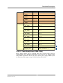
Table 9. Pin assignment of 114-pin side-card connector, pins 1..38
1
39
77
2
40
78
1
GND
2
GND
3
SATA_A_TX+
4
SATA_B_TX+
5
SATA_A_TX-
6
SATA_B_TX-
7
GND
8
GND
9
SATA_A_RX+
10
SATA_B_RX+
11
SATA_A_RX-
12
SATA_B_RX-
13
GND
14
GND
15
PCIE1_TX+
16
PCIE3_TX+
17
PCIE1_TX-
18
PCIE3_TX-
19
GND
20
GND
21
PCIE1_RX+
22
PCIE3_RX+
23
PCIE1_RX-
24
PCIE3_RX-
25
GND
26
GND
27
PCIE0_TX+
28
PCIE2_TX+
29
PCIE0_TX-
30
PCIE2_TX-
31
GND
32
GND
33
PCIE0_RX+
34
PCIE2_RX+
35
PCIE0_RX-
36
PCIE2_RX-
37
GND
38
GND
GND
Note: The SATA channel is not available if this channel is used for rear I/O. It can
be switched to SATA_A or to SATA_B via BIOS settings..
The PCI Express lanes are only available if they are not used for rear I/O.
See Chapter 2.8.4 Serial ATA (SATA) on page 29 and Chapter 3 BIOS on page
52) on how to switch to SATA_A or to SATA_B via BIOS settings.
MEN Mikro Elektronik GmbH
20F019P00 E6 – 2015-01-13
37
Functional Description
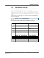
Table 10. Pin assignment of 114-pin side-card connector, pins 39..76
39
77
MEN Mikro Elektronik GmbH
20F019P00 E6 – 2015-01-13
40
78
39
+3.3V
40
+3.3V
41
USB_2_3_OC#
42
HDA_SYNC
43
USB_4_5_OC#
44
HDA_BIT_CLK
45
GND
46
HDA_RST#
47
USB_D3-
48
HDA_SDOUT
49
USB_D3+
50
HDA_SDIN
51
GND
52
GND
53
USB_D2-
54
PCIE_WAKE#
55
USB_D2+
56
PLT_RST#
57
GND
58
LINKCAP
59
USB_D5-
60
SMB_CLK
61
USB_D5+
62
SMB_DATA
63
GND
64
GND
65
USB_D4-
66
SDVOCTRL_CLK
67
USB_D4+
68
SDVOCTRL_DATA
69
GND
70
GND
71
PCIE_CLK_A_REF+
72
PCIE_CLK_B_REF+
73
PCIE_CLK_A_REF-
74
PCIE_CLK_B_REF-
75
GND
76
GND
+5V
38
Functional Description
Table 11. Pin assignment of 114-pin side-card connector, pins 77..114
39
77
113
MEN Mikro Elektronik GmbH
20F019P00 E6 – 2015-01-13
40
78
114
77
GND
78
GND
79
SDVO_TVCLKIN-
80
SDVO_FLDSTALL-
81
SDVO_TVCLKIN+
82
SDVO_FLDSTALL+
83
GND
84
GND
85
SDVOB_BLUE-
86
SDVOC_BLUE-
87
SDVOB_BLUE+
88
SDVOC_BLUE+
89
GND
90
GND
91
SDVOB_GREEN-
92
SDVOC_GREEN-
93
SDVOB_GREEN+
94
SDVOC_GREEN+
95
GND
96
GND
97
SDVOB_RED-
98
SDVOC_RED-
99
SDVOB_RED+
100
SDVOC_RED+
101
GND
102
GND
103
SDVOB_CLK-
104
SDVOC_CLK-
105
SDVOB_CLK+
106
SDVOC_CLK+
107
GND
108
GND
109
SDVOB_INT-
110
SDVOC_INT-
111
SDVOB_INT+
112
SDVOC_INT+
113
GND
114
GND
GND
39
Functional Description
Table 12. Signal mnemonics of 114-pin side-card connector
Signal
Power
Direction
Function
+3.3V
out
+3.3 V power supply
+5V
out
+5 V power supply
GND
-
Digital ground of respective interface
SATA_A_RX+,
SATA_A_RX-
in
Differential pair of SATA receive lines, port A
(not available if used for rear I/O)
SATA_A_TX+,
SATA_A_TX-
out
Differential pair of SATA transmit lines, port A
(not available if used for rear I/O)
SATA_B_RX+,
SATA_B_RX-
in
Differential pair of SATA receive lines, port B
(not available if used for rear I/O)
SATA_B_TX+,
SATA_B_TX-
out
Differential pair of SATA transmit lines, port B
(not available if used for rear I/O)
PCI
Express
PCIE_CLK_A_REF+,
PCIE_CLK_A_REF-
out
Reference clock A 100 MHz
(not
available if
used for
rear I/O)
PCIE_CLK_B_REF+,
PCIE_CLK_B_REF-
out
Reference clock B 100 MHz
PCIE0_RX+,
PCIE0_RX-
in
Differential pair of PCIe receive lines, port 0
PCIE0_TX+,
PCIE0_TX-
out
Differential pair of PCIe transmit lines, port 0
PCIE1_RX+,
PCIE1_RX-
in
Differential pair of PCIe receive lines, port 1
PCIE1_TX+,
PCIE1_TX-
out
Differential pair of PCIe transmit lines, port 1
PCIE2_RX+,
PCIE2_RX-
in
Differential pair of PCIe receive lines, port 2
PCIE2_TX+,
PCIE2_TX-
out
Differential pair of PCIe transmit lines, port 2
PCIE3_RX+,
PCIE3_RX-
in
Differential pair of PCIe receive lines, port 3
PCIE3_TX+,
PCIE3_TX-
out
Differential pair of PCIe transmit lines, port 3
PCIE_WAKE#
in
Wake signal from PCIe device to wake F19P
from sleep state
SATA (one
port which
can be
switched to
SATA_A or
SATA_B)
MEN Mikro Elektronik GmbH
20F019P00 E6 – 2015-01-13
40
Functional Description
Signal
USB
HD Audio
Serial
Digital
Video
Output
(SDVO)
Direction
Function
USB_D[2]+,
USB_D[2]-
in/out
Differential pair of USB lines, port 2
USB_D[3]+,
USB_D[3]-
in/out
Differential pair of USB lines, port 3
USB_D[4]+,
USB_D[4]-
in/out
Differential pair of USB lines, port 4
USB_D[5]+,
USB_D[5]-
in/out
Differential pair of USB lines, port 5
USB_OC23#
in
USB overcurrent, ports 2 and 3
USB_OC45#
in
USB overcurrent, ports 4 and 5
HDA_BIT_CLK
in/out
HD Audio serial data clock
HDA_RST#
out
HD Audio reset
HDA_SDIN
in
HD Audio serial data in
HDA_SDOUT
out
HD Audio serial data out
HDA_SYNC
out
HD Audio synchronization
SDVOB_BLUE+,
SDVOB_BLUE-
out
Serial digital video B blue data, differential pair
SDVOB_GREEN+,
SDVOB_GREEN-
out
Serial digital video B green data, differential pair
SDVOB_RED+,
SDVOB_RED-
out
Serial digital video B red data, differential pair
SDVOB_CLK+,
SDVOB_CLK-
out
Serial digital video B clock, differential pair
SDVOB_INT+,
SDVOB_INT-
in
Serial digital video B input interrupt, differential
pair
SDVOC_BLUE+,
SDVOC_BLUE-
out
Serial digital video C blue data, differential pair
SDVOC_GREEN+,
SDVOC_GREEN-
out
Serial digital video C green data, differential pair
SDVOC_RED+,
SDVOC_RED-
out
Serial digital video C red data, differential pair
SDVOC_CLK+,
SDVOC_CLK-
out
Serial digital video C clock, differential pair
SDVOC_INT+,
SDVOC_INT-
in
Serial digital video C input interrupt, differential
pair
SDVO_FLDSTALL+,
SDVO_FLDSTALL-
in
Serial digital video field stall, differential pair
SDVO_TVCLKIN+,
SDVO_TVCLKIN-
in
Serial digital video TVOUT synchronization
clock, differential pair
SDVOCTRL_CLK
in/out
I2C based control signal (clock) for SDVO device
SDVOCTRL_DATA
in/out
I2C based control signal (data) for SDVO device
MEN Mikro Elektronik GmbH
20F019P00 E6 – 2015-01-13
41
Functional Description
Signal
Other
Direction
Function
LINKCAP
in
LINKCAP indicates how the CompactPCI
Express backplane system slot is routed (2-Link
combined or 4-Link configuration).
PLT_RST#
out
Platform reset (global reset)
SMB_CLK
out
System Management Bus clock
SMB_DATA
in/out
System Management Bus data
MEN Mikro Elektronik GmbH
20F019P00 E6 – 2015-01-13
42
Functional Description
2.13.2
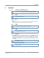
Installing a Side Card
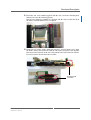
Perform the following steps to install a side card:
Power-down your system and remove the F19P from the system.
Remove the front panel: Loosen and remove the screws highlighted in red.
CompactPCI ®
RST
STA
1
2 3
4
Front‐panel mounting screws at bottom side of board
VGA
F19P
Remove the frontpanel ejector from
the F19P front
panel: Loosen the
ejector screw at the
back of the front
panel.
Install the ejector
on the side card’s
front panel.
MEN Mikro Elektronik GmbH
20F019P00 E6 – 2015-01-13
43
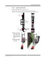
Functional Description
Install the side card standoff supplied with the side card in the mounting hole
indicated in red in the following picture.
Note that two different standoffs are supplied with the side card. For the F19P
the shorter standoff (M2x12 I/A) is required.
Each side card comes with a dedicated one-piece, two-slot front panel. Align
the F19P’s front panel connectors with the side card’s front panel, and align the
board-to-board connector of the side card with the side-card connector of F19P.
Press the board-to-board connectors together.
Board-to-board
connection
MEN Mikro Elektronik GmbH
20F019P00 E6 – 2015-01-13
44
Functional Description
Fasten the front panel: Install the screws removed before as highlighted in red.
CompactPCI ®
RST
STA
1
2 3
4
Front‐panel mounting screws at bottom side of board
VGA
F19P
Fasten the side-card standoff using the spring and screw provided with the side
card at the top of the side card.
Reinsert the board into your system.
MEN Mikro Elektronik GmbH
20F019P00 E6 – 2015-01-13
45
Functional Description
2.14
PCI Express
2.14.1
General
PCI Express (PCIe) succeeds PCI and AGP and offers higher data transfer rates.
As opposed to the PCI bus, PCIe is no parallel bus but a serial point-to-point
connection. Data is transferred using so-called lanes, with each lane consisting of a
line pair for transmission and a second pair for reception. Individual components are
connected using switches.
PCIe supports full-duplex operation and uses a clock rate of 1.25 GHz DDR. This
results in a data rate of max. 250 MB/s per lane in each direction. (The standard PCI
bus with 32 bits/33 MHz only allows a maximum of 133 MB/s.)
If you use only one lane, you speak of a PCIe x1 link. You can couple several lanes
to increase the data rate, e.g. x2 with 2 lanes up to a x32 link using 32 lanes.
In addition, PCIe supports hot plug, for instance to exchange defect expansion
boards during operation.
In terms of software, most operating systems can handle PCI Express boards just as
well as the old PCI.
2.14.2
Implementation on F19P
On F19P the two Gigabit Ethernet channels are permanently connected via two
PCIe x1 links. Another four x1 links are available for use over a side card. This
means that the side card implementation determines the usage of these four links.
Alternatively, these four interfaces can be led to the J2 rear I/O connector in
compliance with the CompactPCI PlusIO standard PICMG 2.30.
The Northbridge of the F19P provides an additional PCI Express link over the PEG
(PCI Express Graphics) port. This link is used to connect the rear I/O Gigabit
Ethernet interface.
MEN Mikro Elektronik GmbH
20F019P00 E6 – 2015-01-13
46
Functional Description
2.15
CompactPCI Interface
2.15.1
General
The F19P is a 3U CompactPCI system slot board. It implements a 32-bit PCI
interface to the CompactPCI backplane which uses a +3.3 V signaling voltage. It
also tolerates +5 V.
The CompactPCI bus connects directly to the Southbridge. The board supports
seven external PCI bus masters.
In combination with a specific side card the F19P can also perform system-slot
functionality in a CompactPCI Express system.
2.15.2
CompactPCI PlusIO Rear I/O
The F19P is also compliant to the CompactPCI PlusIO standard PICMG 2.30. This
means that it offers a fixed pin assignment of 1 Gigabit Ethernet, 4 SATA, 4 PCI
Express and 4 USB interfaces at the J2 connector.
As a result, the pin assignment of the F19P rear I/O connector J2 is not compliant
anymore to the rear I/O of the F14, F15, F17 and F18.
If you use four PCI Express x1 links via the J2 connector, no PCI Express is
available via the side-card connector.
MEN offers a rear I/O transition module on which all interfaces from the J2
connector can be accessed, the CT12.
See MEN’s website for further information.
The pin assignment of connector J1 as defined in the CompactPCI specification will
not be repeated here. The table below shows the fixed pinout of the J2 connector.
Note: The F19P supports one Gigabit Ethernet interface at the rear whereas the
PICMG 2.30 CompactPCI PlusIO standard supports up to two.
MEN Mikro Elektronik GmbH
20F019P00 E6 – 2015-01-13
47
Functional Description
Table 13. Pin assignment of CompactPCI connector J2
F
F E D C B A Z
22
21
1
E
D
C
B
A
Z
22 GND
-
GA1
GA2
GA3
GA4
GND
21 GND
1_ETH_B+
1_ETH_D+
-
GND
CLK6
GND
20 GND
1_ETH_B-
1_ETH_D-
-
GND
CLK5
GND
19 GND
1_ETH_A+
1_ETH_C+
-
GND
GND
GND
18 GND
1_ETH_A-
1_ETH_C-
-
-
-
GND
17 GND
GNT6#
REQ6#
PBRST#
-
-
GND
16 GND
-
GND
DEG#
2_PE_CLK+
4_PE_CLK-
GND
15 GND
GNT5#
REQ5#
FAIL#
2_PE_CLK-
4_PE_CLK+
GND
14 GND C_PWRBTN
SATA_SCL
4_PE_CLKE# 1_PE_CLK+
3_PE_CLK-
GND
13 GND
SATA_SDO
3_PE_CLKE# 1_PE_CLK-
3_PE_CLK+
GND
12 GND 4_SATA_Rx+
SATA_SDI
2_PE_CLKE# 1_PE_CLKE# 4_PE_Rx00+ GND
11 GND 4_SATA_Rx-
4_SATA_Tx+
9_USB2+
4_PE_Tx00+ 4_PE_Rx00-
10 GND 3_SATA_Rx+
4_SATA_Tx-
9_USB2-
4_PE_Tx00- 3_PE_Rx00+ GND
9
GND
3_SATA_Rx-
3_SATA_Tx+
8_USB2+
3_PE_Tx00+ 3_PE_Rx00-
8
GND 2_SATA_Rx+
3_SATA_Tx-
8_USB2-
3_PE_Tx00- 2_PE_Rx00+ GND
7
GND
2_SATA_Rx-
2_SATA_Tx+
7_USB2+
2_PE_Tx00+ 2_PE_Rx00-
6
GND 1_SATA_Rx+
2_SATA_Tx-
7_USB2-
2_PE_Tx00- 1_PE_Rx00+ GND
5
GND
1_SATA_Rx-
1_SATA_Tx+
6_USB2+
1_PE_Tx00+ 1_PE_Rx00-
GND
4
GND
-
1_SATA_Tx-
6_USB2-
1_PE_Tx00-
-
GND
3
GND
GNT4#
REQ4#
GNT3#
GND
CLK4
GND
2
GND
REQ3#
GNT2#
-
CLK3
CLK2
GND
1
GND
REQ2#
GNT1#
REQ1#
GND
CLK1
GND
MEN Mikro Elektronik GmbH
20F019P00 E6 – 2015-01-13
SATA_SL
GND
GND
GND
48
Functional Description
Table 14. Signal mnemonics of CompactPCI connector J2 – CompactPCI and
CompactPCI PlusIO rear I/O
Signal
CompactPCI CLK[6:1]
Ethernet
SATA
SGPIO
MEN Mikro Elektronik GmbH
20F019P00 E6 – 2015-01-13
Direction
Function
out
Clocks 1 to 6
PBRST#
in
Push button reset
DEG#
in
Power supply degenerate
FAIL#
in
Power supply fail
C_PWRBTN#
in
Power button, optional
REQ#/GNT#[6:1]
in/out
Request/grant pairs 1 to 6
1_ETH_A+,
1_ETH_A-
in/out
Differential data pair 0, Ethernet
port 1
1_ETH_B+,
1_ETH_B-
in/out
Differential data pair 1, Ethernet
port 1
1_ETH_C+,
1_ETH_C-
in/out
Differential data pair 2, Ethernet
port 1
1_ETH_D+,
1_ETH_D-
in/out
Differential data pair 3, Ethernet
port 1
1_SATA_Rx+,
1_SATA_Rx-
in
Differential pair of SATA receive
lines, port 1
1_SATA_Tx+,
1_SATA_Tx-
out
Differential pair of SATA transmit
lines, port 1
2_SATA_Rx+,
2_SATA_Rx-
in
Differential pair of SATA receive
lines, port 2
2_SATA_Tx+,
2_SATA_Tx-
out
Differential pair of SATA transmit
lines, port 2
3_SATA_Rx+,
3_SATA_Rx-
in
Differential pair of SATA receive
lines, port 3
3_SATA_Tx+,
3_SATA_Tx-
out
Differential pair of SATA transmit
lines, port 3
4_SATA_Rx+,
4_SATA_Rx-
in
Differential pair of SATA receive
lines, port 4
4_SATA_Tx+,
4_SATA_Tx-
out
Differential pair of SATA transmit
lines, port 4
SATA_SC
out
Clock signal
SATA_SL
out
Last clock of a bit stream; begin a
new bit stream on the next clock
SATA_SDO
out
Serial data output bit stream
SATA_SDI
in
Serial data input bit stream (may
not be supported by all SGPIO
devices)
49
Functional Description
Signal
USB
Direction
Function
6_USB2+,
6_USB2-
in/out
Differential pair of USB lines, port
6
7_USB2+,
7_USB2-
in/out
Differential pair of USB lines, port
7
8_USB2+,
8_USB2-
in/out
Differential pair of USB lines, port
8
9_USB2+,
9_USB2-
in/out
Differential pair of USB lines, port
9
in
Differential PCIe receive lines,
lane 1
1_PE_Tx00+,
1_PE_Tx00-
out
Differential PCIe transmit lines,
lane 1
2_PE_Rx00+,
2_PE_Rx00-
in
Differential PCIe receive lines,
lane 2
2_PE_Tx00+,
2_PE_Tx00-
out
Differential PCIe transmit lines,
lane 2
3_PE_Rx00+,
3_PE_Rx00-
in
Differential PCIe receive lines,
lane 3
3_PE_Tx00+,
3_PE_Tx00-
out
Differential PCIe transmit lines,
lane 3
4_PE_Rx00+,
4_PE_Rx00-
in
Differential PCIe receive lines,
lane 4
4_PE_Tx00+,
4_PE_Tx00-
out
Differential PCIe transmit lines,
lane 4
[1..4]_PE_CLKE#
in
Presence detect, PCIe lane 1..4
[1..4]_PE_CLK-,
[1..4]_PE_CLK+
out
Differential 100 MHz Reference
Clock, PCIe lane 1..4
PCI Express 1_PE_Rx00+,
1_PE_Rx00-
2.15.2.1 Power Supply Status (DEG#, FAIL#)
Power supply failures may be detected before the system crashes down by
monitoring the signals DEG# or FAIL#. These active-low lines are additions of the
CompactPCI specification and may be driven by the power supply. DEG# signals
the degrading of the supply voltages, FAIL# their possible failure.
MEN Mikro Elektronik GmbH
20F019P00 E6 – 2015-01-13
50
Functional Description
2.16
Reset Button and Status LED
The F19P has a reset button and one status LED at the front panel. The reset button
is recessed within the front panel and requires a tool, e.g. paper clip to be pressed,
preventing the button from being inadvertently activated.
The yellow status LED shows board status messages. The LED is controlled by a
GPIO pin of the board controller. It is switched on when the BIOS starts, switched
off when the board is switched off and flashing when the board is in stand-by (S3)
status.
During normal operation the LED can be switched on and off using the MEN driver
for the board controller.
See MEN’s website for further information.
In case of a board failure, the LED displays the following error messages:
Table 15. Error codes signaled by board management controller via LED flashes
Number
of
Flashes
Description
1
XM02BCI_ERR_33A
3.3 V failure
2
XM02BCI_ERR_INP
Input voltage failure
3
XM02BCI_ERR_NO_EXT_PWR_OK
External power supply
failure
4
XM02BCI_ERR_ICH_HANDSHAKE
Chipset handshake failure
5
XM02BCI_ERR_NO_DDRVR_PWRGD
Memory voltage failure
6
XM02BCI_ERR_NO_PWRGD_5130
1.05 V or internal 3.3 V
voltage failure
7
XM02BCI_ERR_NO_IMVP_PWRGD
CPU voltage failure
8
XM02BCI_ERR_NO_GFX_PWRGD
Graphic voltage failure
9
XM02BCI_ERR_PLT_RST_TIMEOUT
Platform reset timeout
10
XM02BCI_ERR_CPU_RST_TIMEOUT
CPU Reset timeout
11
XM02BCI_ERR_BIOS_TIMEOUT
BIOS timeout
12
XM02BCI_ERR_CPU_TOO_HOT
CPU too hot
255
CPUBCI_INVALID_MAIN_STATE
Invalid PIC main state
MEN Mikro Elektronik GmbH
20F019P00 E6 – 2015-01-13
Error
51
BIOS
3
BIOS
The F19P is equipped with an InsydeH2O setup utility from Insyde Software.
InsydeH2O is Insyde Software's firmware product line designed to replace
traditional PC BIOS. It is an implementation of the Intel's Platform Innovation
Framework for UEFI /EFI. The UEFI/EFI specification defines a new model for the
interface between operating systems and platform firmware. This interface consists
of data tables that contain platform-related information, plus boot and runtime
service calls that are available to the operating system and its loader. Together, these
provide a standard environment for booting an operating system and running preboot applications. This product line is the next generation of PC BIOS technology.
The ">" character in front of a menu item means that a sub-menu is available. An
"x" in front of a menu item means that there is a configuration option which needs to
be activated through a higher configuration option before being accessible.
MEN Mikro Elektronik GmbH
20F019P00 E6 – 2015-01-13
52
BIOS
3.1
Main
InsydeH2O Setup Utility
Main
Advanced
Security
Power
Rev. 3.5
Boot
Exit
InsydeH2O Version
F19P BIOS V 1.xx
Processor Type
Intel Celeron M CPU 722 @ 1.20GHz
System Bus Speed
800MHz
System Memory Speed
800MHz
Cache RAM
1024kB
Total Memory
2048MB
SODIMM 0
1024MB
SODIMM 1
1024MB
System Time
[hh:mm:ss]
System Date
[mm/dd/yyyy]
F1 Help
Select Item
F5/F6 Change Values
F9 Setup Defaults
Esc Exit
Select Menu
Enter Select >
Submenu
F10 Save and Exit
InsydeH2O Version / MEN Board / Processor Type / System Bus Speed
/ System Memory Speed / Cache RAM/ Total Memory/ SODIMM 0 /
SODIMM 1
Description
You cannot change any values in these fields. They are only for
information.
Language
Description
Select the default language
Options
English
System Time
Description
MEN Mikro Elektronik GmbH
20F019P00 E6 – 2015-01-13
Change the internal clock.
53
BIOS
Options
hh
Hours (Valid range from 0 to 23)
mm
Minutes (Valid range from 0 to 59)
ss
Seconds (Valid range from 0 to 59)
System Date
Description
Change the date
Options
mm
Month (Valid range from 1 to 12)
dd
Day (Valid range from 1 to 31)
yyyy
Year (Valid range from 2000 to 2099)
MEN Mikro Elektronik GmbH
20F019P00 E6 – 2015-01-13
54
BIOS
3.2
Advanced
InsydeH2O Setup Utility
Main
Advanced
Security
Power
Rev. 3.5
Boot
Exit
>Boot Configuration
>Peripheral Configuration
>IDE Configuration
>Video Configuration
>USB Configuration
>Chipset Configuration
>ACPI Table/Features Control
>PCI Express Root Port 1
>PCI Express Root Port 2
>PCI Express Root Port 3
>PCI Express Root Port 4
>PCI Express Root Port 5
>PCI Express Root Port 6
F1 Help
Select Item
F5/F6 Change Values
F9 Setup Defaults
Esc Exit
Select Menu
Enter Select >
Submenu
F10 Save and Exit
MEN Mikro Elektronik GmbH
20F019P00 E6 – 2015-01-13
55
BIOS
Boot Configuration — Sub-menu
NumLock
Power Supply Type
Watchdog
SMI Handler
PWRON after PWR-Fail
ATX_PWRGD Failure Mode
Spread Spectrum Control
[On]
[AT]
[Off]
[On]
[On]
[Check at Start-Up]
[On]
MEN F19P Settings
SATA-4 Switch
x Port Switch
PCIe Switch
[On]
[Port A]
[On]
Numlock
Description
Selects power-on state for Numlock
Options
On
Off
Power Supply Type
Description
Selects the type of power supply
Options
AT
ATX
Watchdog
Description
Enables or disables the F19P Watchdog
Options
Off
10 min
1 min
15 min
2 min
20 min
5 min
30 min
SMI Handler
Description
Enables or disables the SMI functionality
Options
On
Off
PWRON after PWR-Fail
Description
Sets the system power status when power returns to the system
from a power failure situation.
Options
On
Off
Former State
ATX_PWRGD Failure Mode
Description
Determines the system behavior in case of a failure at the ATX
power good signal
Options
Check at Start-Up Check always
Spread Spectrum Control
Description
Enable or disable Spread Spectrum
Options
On
MEN Mikro Elektronik GmbH
20F019P00 E6 – 2015-01-13
Spread Spectrum enabled
56
BIOS
Off
Spread Spectrum disabled
MEN F19P Settings
SATA-4 Switch
Description
Switch for the SATA-4 interface.
Options
On
SATA-4 available at side card
Off
SATA-4 available at rear I/O
Port Switch
Description
Select one of the two available ports on the side card (only if
menu item SATA-4 Switch is [On]
Options
Port A
SATA Port A is selected
Port B
SATA Port B is selected
PCIe Switch
Description
Switch for the PCIe Ports 1-4.
Options
On
PCIe Ports 1-4 are routed to the side card.
Off
PCIe Ports are routed to rear I/O
MEN Mikro Elektronik GmbH
20F019P00 E6 – 2015-01-13
57
BIOS
Peripheral Configuration — Sub-menu
HD Audio
LAN-1
LAN-2
[Auto]
[On]
[On]
F19P Settings
>LAN-3
[On]
HD Audio
Description
Enable or disable the HD Audio controller.
Options
Auto
The controller is enabled if a codec is found.
Disabled
The controller is disabled even when there is
an audio codec.
Enabled
The controller is enabled independent of the
presence of a codec.
LAN-1/LAN-2/LAN-3
Description
Enables or disables the LAN interfaces.
Options
On
MEN Mikro Elektronik GmbH
20F019P00 E6 – 2015-01-13
Off
58
BIOS
IDE Configuration — Sub-menu
IDE Controller
[Enabled]
Delay for HDD
[Off]
Force SATA Speed to Gen-1
(1.5 Gb/s)
[Disabled]
HDC Configure as
[AHCI]
SGPIO Interface
[Off]
SATA Port 0 - HotPlug
[Enabled]
Port 0 External
[Disabled]
SATA Port 1 - HotPlug
[Enabled]
Port 1 External
[Disabled]
SATA Port 2 - HotPlug
[Enabled]
Port 2 External
[Disabled]
SATA Port 3 - HotPlug
[Enabled]
Port 3 External
[Disabled]
>Serial ATA Port 1
[ST9160310AS]
Type:
[Auto]
32Bit I/O:
Block Mode:
Transfer Mode:
Security Mode:
>Serial ATA Port 2
Type:
[Enabled]
[Enabled]
[Ultra DMA ATA-100]
Uninstall
[ST960817SM]
[Auto]
32Bit I/O:
Block Mode:
Transfer Mode:
Security Mode:
>Serial ATA Port 3
>Serial ATA Port 4
[Enabled]
[Enabled]
[Ultra DMA ATA-100]
Uninstall
[Not Installed]
[Not Installed]
IDE Controller
Description
Enables or disables the IDE controllers.
Options
Enabled
Disabled
Delay for HDD
Description
Sets the delay for spin-up of the hard disk in seconds.
Options
Off
1 sec
2 sec
3 sec
4 sec
5 sec
6 sec
7 sec
8 sec
9 sec
10 sec
Force SATA Speed to Gen-1 (1.5 Gb/s)
Description
Enabled: The SATA speed is forced to 1.5 Gb/s.
Disabled: The max. SATA speed is 3.0 Gb/s.
Options
Enabled
MEN Mikro Elektronik GmbH
20F019P00 E6 – 2015-01-13
Disabled
59
BIOS
HDC Configure as
Description
Set hard disk controller configure type.
Options
IDE
RAID
AHCI
SGPIO Interface
Description
Starts the chipset’s SGPIO functionality. SGPIO is, e.g., required
for the hot-plug functionality of SATA HDDs, if the Intel Rapid
Storage Manager is used under Windows. Only available if item
HDC Configure as is set to AHCI.
Options
on
off
SATA Port 0/1/2/3 Hot Plug
Description
This setting indicates that the port is hot-plug capable. Only
available if item HDC Configure as is set to AHCI.
Options
Enabled
Disabled
Port 0/1/2/3 External
Description
This setting indicates that the port is an external SATA port. Only
available if item HDC Configure as is set to AHCI.
Options
Enabled
Disabled
Serial ATA Port 1/2
Type
Description
When the option user-defined is set, the items 32Bit I/O, Block
Mode and Transfer Mode can be modified.
Options
Auto
User-defined
32Bit I/O
Description
Enable/disable 32Bit I/O.
Options
Enabled
Disabled
Block Mode
Description
Enable/disable Block Mode.
Options
Enabled
Disabled
Transfer Mode
Description
Sets the Transfer Mode.
Options
Auto
Fast PIO
Ultra DMA ATA-33 Ultra DMA ATA-66
Ultra DMA ATA100
Security Mode
Description
MEN Mikro Elektronik GmbH
20F019P00 E6 – 2015-01-13
No changes can be made here.
60
BIOS
Options
Uninstall
Serial ATA Port 3/4
Description
MEN Mikro Elektronik GmbH
20F019P00 E6 – 2015-01-13
Not installed. You can make no changes here.
61
BIOS
Video Configuration — Sub-menu
Render Standby
Render Thermal Throttling
IGD - Device2, Function1
IGD - Pre-allocated Memory
IGD - DVMT Size
IGD - Boot Type
IGD - LCD Panel Type
IGD - PAVP Mode
IGD - Gfx Low Power Mode
Primary Video
[Enabled]
[Enabled]
[Enabled]
[UMA = 64MB]
[DVMT Max]
[VBIOS Default]
[1024x768 LVDS]
[Lite]
[Enabled]
[PEG]
Render Standby
Description
Check to enable render standby support.
Options
Enabled
Disabled
Render Thermal Throttling
Description
This feature is applicable for Graphic SKUs only
Options
Enabled
Disabled
IGD - Device2, Function1
Description
Enable/Disable function 1 of the internal graphics device by
setting item to the desired value
IGD - Pre-allocated Memory
Description
Select the amount of pre-allocated memory that the Internal
Graphics Device will use. Warning: Some feature may not be
supported with 1MB pre-allocated memory.
Options
UMA = 32 MB
UMA = 64 MB
IGD - DVMT Size
Description
Select the size of DVMT 3.0 that the Internal Graphics Device will
use
Options
64 MB
128 MB
224MB
IGD - Boot Type
Description
Select the Video Device that will be activated during POST
Options
VBIOS Default
CRT
LFP
CRT+LFP
TV
LFP-SDVO
EFP
TV-SDVO
CRT+LFP-SDVO
CRT+EFP
IGD - LCD Panel Type
Description
Select the panel used by the Internal Graphics Device
Options
640x480 LVDS
MEN Mikro Elektronik GmbH
20F019P00 E6 – 2015-01-13
800x600 LVDS
62
BIOS
1024x768 LVDS
1280x1024 LVDS
1400x1050 LVDS1 1400x1050 LVDS2
1600x1200 LVDS
IGD - PAVP Mode
Description
GMCH protected audio video path BIOS support
Options
Disabled
Lite
High
IGD - Gfx Low Power Mode
Description
Applicable for SFF only
Options
Enabled
Disabled
Primary Video
Description
Primary Video Mode for Video Output
Options
IGD
PEG
PCI
PCIe
MEN Mikro Elektronik GmbH
20F019P00 E6 – 2015-01-13
63
BIOS
USB Configuration — Sub-menu
USB Legacy
EHCI 1
EHCI 2
UHCI 1
UHCI 2
UHCI 3
UHCI 4
UHCI 5
UHCI 6
Pre-Port Control
[Enabled]
[Enabled]
[Enabled]
[Enabled]
[Enabled]
[Enabled]
[Enabled]
[Enabled]
[Enabled]
[Disabled]
USB Pre-fetch Feature
USB Pre-fetch Time
USB HC Alignment
[Enabled]
[2ms]
[Enabled]
USB Legacy
Description
If this menu item is enabled it is possible to boot from USB
devices and use a USB keyboard under DOS. Cannot be
changed.
Options
Enabled
EHCI 1/2
Description
Enable/Disable EHCI 1/2.
Options
Enabled
Disabled
UHCI 1
Description
Enable UHCI 1. Cannot be changed.
Options
Enabled
UHCI 2/3/4/5/6
Description
Enable UHCI 2/3/4/5/6.
Options
Enabled
Disabled
Pre-Port Control
Description
Enable/Disable the per port disable control override
Options
Enabled
Disabled
USB Pre-fetch Feature
Description
Enable/Disable the USB pre-fetch Feature
Options
Enabled
Disabled
USB Pre-fetch Time
Description
Select the USB pre-fetch time.
Options
2ms
4ms
USB HC Alignment
Description
Enable/Disable the USB HC Alignment.
Options
Enabled
MEN Mikro Elektronik GmbH
20F019P00 E6 – 2015-01-13
Disabled
64
BIOS
Chipset Configuration
Setup warning
Setting items on this screen to incorrect values may cause your system
to malfunction!
CRID
DMI Link ASPM Control
Automatic ASPM
Manual:--------ASPM L0s Support
ASPM L0sL1 Support
---------------VT-d
System Memory Frequency
[Enabled]
[Enabled]
[Auto]
[Disabled]
[Disabled]
[Enabled]
[Auto]
>Memory Thermal Management
TM Mode
[Disabled]
TS on DIMM
[Disabled]
TM lock
[Disabled]
CRID
Description
Enable or disable : Compatible Revision ID ( CRID ) / Stepping
Revision ID ( SRID )
Options
Enabled
Disabled
DMI Link ASPM Control
Description
Enable or disable the control of Active State Power Management
on both GMCH side and ICH8M side of the DMI Link.
Options
Enabled
Disabled
Automatic ASPM
Description
Automatically or manually control the level of ASPM supported on
the DMI Link.
Options
Auto
Manual
ASPM L0s Support
Description
Control L0s Entry Support on the DMI Link
Options
Enabled
Disabled
ASPM L0sL1 Support
Description
Control L0s and L1 Entry Support on the DMI Link
Options
Enabled
Disabled
VT-d
Description
Check to enable VT-d function on MCH
Options
Enabled
Disabled
System Memory Frequency
Description
Determines the System Memory Frequency.
Options
Auto
MEN Mikro Elektronik GmbH
20F019P00 E6 – 2015-01-13
No change in System Memory Frequency.
65
BIOS
667MHz
System Memory Frequency fixed at 667MHz.
Memory Thermal Management
Description
Configure Memory Thermal Management
TM Mode
Description
Select TM mode. Cannot be changed.
Options
Disabled
TS on DIMM
Description
Enable or disable TS on DIMM. Cannot be changed.
Options
Disabled
TM Lock
Description
Enable or disable TM Lock. Cannot be changed.
Options
Disabled
MEN Mikro Elektronik GmbH
20F019P00 E6 – 2015-01-13
66
BIOS
ACPI Table/Feature Control
FACP - C2 Latency Value
FACP - C3 Latency Value
FACP - RTC S4 Wakeup
APIC - IO APIC Mode
HPET - HPET Support
Enabled:----xBase Address select
[Disabled]
[Disabled]
[Enabled]
[Enabled]
[Enabled
[FED00000h]
FACP - C2 Latency Value
Description
Value only for ACPI. Select the value for the P_LVL2_LAT field
found in the FACP Table where: 1 = C2 Enabled, 101 = C2
Disabled
Options
Enabled
Disabled
FACP - C3 Latency Value
Description
Value only for ACPI. Select the value for the P_LVL3_LAT field
found in the FACP Table where: 57 = C3 Enabled, 1001 = C3
Disabled
Options
Enabled
Disabled
FACP - RTC S4 Wakeup
Description
Value only for ACPI. Enable/Disable for S4 Wakeup from RTC
Options
Enabled
Disabled
APIC - IO APIC Mode
Description
This item is valid only for WIN2k and WINXP.Also, a fresh install
of the OS must occur when APIC Mode is desired.Test the IO
ACPI by setting item to Enable.The APIC Table will then be
pointed to by the RSDT, the Local APIC will be initialized, and the
proper enable bits will be set in ICH4M.
Options
Enabled
Disabled
HPET - HPET Support
Description
High Performance Event Timer Support in Windows XP. If this
feature is enabled, the HPET table will be added into the ACPI
Tables.
Options
Enabled
Disabled
Base Address Select
Description
Memory address ranges of High Performance Event Timer. Only
available if HPET support is enabled.
Options
FED00000h
FED10000h
FED20000h
FED30000h
MEN Mikro Elektronik GmbH
20F019P00 E6 – 2015-01-13
67
BIOS
PCI Express Root Port 1/2/3/4/5/6 Settings
PCI Express Root Port 1 [Enabled]
VC1 Enable
[Disabled]
ASPM
[Enabled]
URR
[Disabled]
FER
[Disabled]
NFER
[Disabled]
CER
[Disabled]
CTO
[Disabled]
SEFE
[Disabled]
SENFE
[Disabled]
SECE
[Disabled]
PME Interrupt
[Disabled]
PME SCI
[Disabled]
Hot Plug SCI
[Disabled]
PCI Express Root Port 1/2/3/4/5/6
Description
If PCI Express Root Port 1 is disabled, PCI Express Root Ports 2
to 6 will also be disabled.
Options
Enabled
Disabled
VC1 Enable
Description
Enable or disable Virtual Channel 1.
Options
Disabled
Auto
ASPM
Description
Enable ASPM settings.
Options
Enabled
Disabled
URR
Description
Enable or disable PCI Express Unsupported Request Reporting.
Options
Enabled
Disabled
FER
Description
Enable or disable PCI Express Device Fatal Error Reporting.
Options
Enabled
Disabled
NFER
Description
Enable or disable Device Non-Fatal Error Reporting.
Options
Enabled
Disabled
CER
Description
Enable or disable PCI Express Device Correctable Error
Reporting.
Options
Enabled
Disabled
CTO
Description
Enable or disable PCI Express Completion Timer.
Options
Enabled
MEN Mikro Elektronik GmbH
20F019P00 E6 – 2015-01-13
Disabled
68
BIOS
SEFE
Description
Enable or disable Root PCI Express System Error on Fatal Error.
Options
Enabled
Disabled
SENFE
Description
Enable or disable Root PCI Express System Error on Non-Fatal
Error.
Options
Enabled
Disabled
SECE
Description
Enable or disable Root PCI Express System Error on Correctable
Error.
Options
Enabled
Disabled
PME Interrupt
Description
Enable or disable Root PCI Express PME Interrupt.
Options
Enabled
Disabled
PME SCI
Description
Enable or disable PME SCI.
Options
Enabled
Disabled
Hot Plug SCI
Description
Enable or disable PCI Express Hot Plug SCI.
Options
Enabled
MEN Mikro Elektronik GmbH
20F019P00 E6 – 2015-01-13
Disabled
69
BIOS
3.3
Security
InsydeH2O Setup Utility
Main
Advanced
Security
Power
Rev. 3.5
Boot
TPM Status
Not Installed
TPM Operation
[No Operation]
Supervisor Password
[Installed/Not Installed]
User Password
[Installed/Not Installed]
Exit
Set Supervisor Password
Power on password
[Disabled]
User Access level
[View Only]
Set User Password
Clear User Password
F1 Help
Select Item
F5/F6 Change Values
F9 Setup Defaults
Esc Exit
Select Menu
Enter Select >
Submenu
F10 Save and Exit
TPM Status
Description
TPM (Trusted Platform Module) Status. Not supported on the F19P.
Options
Not installed
TPM Operation
Description
TPM (Trusted Platform Module) Operation. Not supported on the
F19P.
Options
No operation
Supervisor Password
Description
Shows whether a supervisor password has been entered.
User Password
Description
MEN Mikro Elektronik GmbH
20F019P00 E6 – 2015-01-13
Shows whether a user password has been entered.
70
BIOS
Set Supervisor Password
Description
Enter and confirm the supervisor password under this menu item.
To delete the password enter an empty password.
Power On Password
Description
Select when the password has to be entered.
Options
Enabled
The password has to be entered when the system
starts.
Disabled
The password has to be entered when changing
to the setup menu.
User Access Level
Description
Set the User Access Level.
Options
View Only
Access to InsydeH2O Setup allowed but the fields
cannot be changed.
Full
Any field can be changed except the Supervisor
password.
Limited
Only limited fields can be changed.
Set User Password
Description
Enter and confirm the user password under this menu item.
Clear User Password
Description
MEN Mikro Elektronik GmbH
20F019P00 E6 – 2015-01-13
Clear the user password. Only possible for a supervisor or user in
the access levels full or limited.
71
BIOS
3.4
Power
InsydeH2O Setup Utility
Main
Advanced
Security
Power
Rev. 3.5
Boot
Exit
>Advanced CPU Control
>Platform Power Management
>Break Event
ACPI S3
[Enabled]
Wake on PME
[Disabled]
Wake on Lan
[Disabled]
Auto Wake on S5
[Disabled]
F1 Help
Select Item
F5/F6 Change Values
F9 Setup Defaults
Esc Exit
Select Menu
Enter Select >
Submenu
F10 Save and Exit
MEN Mikro Elektronik GmbH
20F019P00 E6 – 2015-01-13
72
BIOS
Advanced CPU Control – Sub-Menu
TXT
P-States(IST)
Boot Performance Mode
Thermal Mode
CMP Support
Use XD Capability
VT Support
SMRR Support
C-States
Enhanced C-States
C-State Pop Up Mode
C-State Pop Down Mode
C4 Exit Timing Mode
DeepC4
Hard C4E
Enable C6
EMTTM
Dynamic FSB Switching
[Disable]
[Enabled]
[Max Performance]
[Disabled]
[Auto]
[Enabled]
[Disabled]
[Auto]
[Enabled]
[Enabled]
[Enabled]
[Enabled]
[Fast]
[Enabled]
[Enabled]
[Enabled]
[Enabled]
[Enabled]
Turbo Mode
ACPI 3.0 T-States
DTS
DTS Calibration
[Enabled]
[Disabled]
[Enabled]
[Enabled]
>Thermal Trip Points Setting
Throttle On Temperature [85øC]
TXT
Description
Enables utilization of additional hardware capabilities provided by
Intel Trusted Execution Technology; changes require a full power
cycle to take effect.
Options
Enabled
Disabled
P-States (IST)
Description
Enable processor performance states (P-States).
Options
Enabled
Disabled
Boot Performance Mode
Description
Select the performance state that BIOS will set before OS
handoff.
Options
Max Performance Max Battery
Thermal Mode
Description
Select the Thermal Mode.
Options
Disabled
TM1
TM2
TM1 and TM2
CMP Support
Description
MEN Mikro Elektronik GmbH
20F019P00 E6 – 2015-01-13
Enable or disable core multi processing.
73
BIOS
Options
Auto
Disabled
Use XD Capability
Description
Enable or disable XD capability.
Options
Enabled
Disabled
VT Support
Description
Enable or disable Vanderpool technology.
Options
Enabled
Disabled
SMRR Support
Description
Enable or disable SMRR Support.
Options
Auto
Disabled
C-States
Description
Enable processor idle power saving states (C-States).
Options
Enabled
Disabled
Enhanced C-States
Description
Enable P-State transitions to occur in combination with C-States.
Options
Enabled
Disabled
C-State Pop Up Mode
Description
If enabled and ICH abserves a bus master request, it will take the
system from C3/C4 to C2 and auto enable bus masters. If
disabled, bus master traffic is a break event and ICH will attempt
to return to C0 state.
Options
Enabled
Disabled
C-State Pop Down Mode
Description
If enabled and ICH abserves no bus master requests, it can
return to the previous C3/C4 state. If disabled, ICH will not
attempt to automatically return to the previous C3/C4 state.
Options
Enabled
Disabled
C4 Exit Timing Mode
Description
This option controls a programmable time for the CPU voltage to
stabilize when exiting from a C4 state.
Options
Fast
Default
Slow
Force Slow
DeepC4
Description
Enable Deep C4 with L2 Cache disable instead of C4.
Options
Enabled
Disabled
Hard C4E
MEN Mikro Elektronik GmbH
20F019P00 E6 – 2015-01-13
74
BIOS
Description
Enable P-State transitions to minimum state on C4E.
Options
Enabled
Disabled
Enable C6
Description
Enables or disables the C6 state (Deep Power Down
Technology).
Options
Enabled
Disabled
EMTTM
Description
Enable processor Enhanced Multi Threaded Thermal Monitoring
(requires GV3).
Options
Enabled
Disabled
Dynamic FSB Switching
Description
Enable or disable processor Dynamic FSB Frequency Switching
(Bus GV)
Options
Enabled
Disabled
Turbo Mode
Description
Enable processor Turbo Mode (requires EMTTM enabled too).
Options
Enabled
Disabled
ACPI 3.0 T-States
Description
Enable or disable ACPI 3.0 T-States
Options
Enabled
Disabled
DTS
Description
Enables CPU Digital Thermal Sensor function.
Options
Enabled
Disabled
DTS Calibration
Description
Enables Calibration function.
Options
Enabled
Disabled
>Thermal Trip Points Setting
Throttle On Temperature
Description
Set the CPU temperature point at which the throttle is activated.
Options
40°C
45°C
50°C
55°C
60°C
65°C
70°C
75°C
80°C
85°C
90°C
MEN Mikro Elektronik GmbH
20F019P00 E6 – 2015-01-13
75
BIOS
Platform Power Management – Sub-Menu
PCI Clock Run
[Enabled]
PCI Clock Run
Description
If Enabled,the CLKRUN# Logic will stop the PCI Clocks.
Options
Enabled
Disabled
Break Event – Sub-Menu
Storage Break Event
PCIE Break Event
PCI Break Event
EHCI Break Event
UHCI Break Event
HDA Break Event
[Disabled]
[Disabled]
[Disabled]
[Disabled]
[Disabled]
[Disabled]
Storage Break Event
Description
If Enabled, Parallel IDE or Serial ATA master activity will cause
BM_STS to be set and will cause a break from C3/C4.
Options
Enabled
Disabled
PCIE Break Event
Description
If Enabled, PCI Express master activity will cause BM_STS to be
set and will cause a break from C3/C4.
Options
Enabled
Disabled
PCI Break Event
Description
If Enabled, PCI master activity will cause BM_STS to be set and
will cause a break from C3/C4.
Options
Enabled
Disabled
EHCI Break Event
Description
If Enabled, EHCI master activity will cause BM_STS to be set and
will cause a break from C3/C4.
Options
Enabled
Disabled
UHCI Break Event
Description
If Enabled, UHCI master activity will cause BM_STS to be set and
will cause a break from C3/C4.
Options
Enabled
Disabled
HDA Break Event
Description
If Enabled, Intel High Definition Audio master activity will cause
BM_STS to be set and will cause a break from C3/C4.
Options
Enabled
Disabled
ACPI S3
Description
MEN Mikro Elektronik GmbH
20F019P00 E6 – 2015-01-13
Enable/Disable ACPI S1/S3 Sleep state
76
BIOS
Options
Enabled
Disabled
Wake on PME
Description
Determines the action taken when the system power is off and a
PCI Power Management Enable wake up event occurs.
Options
Enabled
Disabled
Wake on Lan
Description
Determines the action taken when the system power is off and a
Wake on Lan event occurs.
Options
Enabled
Disabled
Auto Wake on S5
Description
Auto wake on S5, By Day of Month or Fixed time of every day
Options
Disabled
By every day
By day of month
MEN Mikro Elektronik GmbH
20F019P00 E6 – 2015-01-13
77
BIOS
3.5
Boot
InsydeH2O Setup Utility
Main
Advanced
Security
Power
UEFI Boot
[Enabled]
Quick Boot
[Enabled]
Quiet Boot
[Enabled]
PXE Boot to LAN
[Disabled]
ACPI Selection
[ACPI 3.0]
USB Boot
[Enabled]
Rev. 3.5
Boot
Exit
>EFI
>Legacy
F1 Help
Select Item
F5/F6 Change Values
F9 Setup Defaults
Esc Exit
Select Menu
Enter Select >
Submenu
F10 Save and Exit
UEFI Boot
Description
Enable/Disable UEFI Boot Function
Options
Enabled
Disabled
Quick Boot
Description
Allows InsydeH2O to skip certain tests while booting. This will
decrease the time needed to boot the system.
Options
Enabled
Disabled
Quiet Boot
Description
Disables or enables booting in Text Mode
Options
Enabled
Disabled
PXE Boot to LAN
Description
MEN Mikro Elektronik GmbH
20F019P00 E6 – 2015-01-13
Disables or enables PXE boot to LAN.
78
BIOS
Options
Enabled
Disabled
ACPI Selection
Description
Select booting to Acpi3.0/Acpi1.0B
Options
Acpi3.0/
Acpi1.0B
USB Boot
Description
Disables or enables booting to USB boot devices.
Options
Enabled
Disabled
EFI – Sub-Menu
EFI
Windows Boot Manager
EFI Boot Menu
Description
MEN Mikro Elektronik GmbH
20F019P00 E6 – 2015-01-13
Selects the boot order for (U)EFI boot media. Windows 7 64-Bit
can be installed in UEFI mode, for example.
79
BIOS
Legacy – Sub-Menu
Boot Device Priority
> Normal Boot Menu
[Normal/Advance]
Normal
Advance
> Boot Type Order
KingstonDataTraveler G3
Floppy Drive
Hard Disk Drive
CD/DVD-ROM Drive
USB
Others
> USB
KingstonDataTraveler G3
Normal Boot Menu
Description
Selects the type of boot order
Options
Normal
Sub-menu Boot Type Order:
Under this menu option it is possible to select
the boot order of device groups (e.g. Hard
Disk before Floppy Drive).
Sub-menu USB:
Under this menu option it is possible to select
the boot order of single devices within a
device group, e.g. USB-HDD before SATAHDD
Advance
Under this menu option there are no device
groups. The single devices are listed and can
be moved to select the boot order, e.g.:
SATA-HDD1
USB-Floppy
USB-DVD-DRIVE
SATA-HDD2
MEN Mikro Elektronik GmbH
20F019P00 E6 – 2015-01-13
80
BIOS
3.6
Exit
InsydeH2O Setup Utility
Main
Advanced
Security
Power
Rev. 3.5
Boot
Exit
Exit Saving Changes
Save Change Without Exit
Exit Discarding Changes
Load Optimal Defaults
Load Custom Defaults
Save Custom Defaults
Discard Changes
F1 Help
Select Item
F5/F6 Change Values
F9 Setup Defaults
Esc Exit
Select Menu
Enter Select >
Submenu
F10 Save and Exit
3.6.1
Exit Saving Changes
Exit system setup and save your changes.
3.6.2
Save Change Without Exit
Save your changes without exiting the system.
3.6.3
Exit Discarding Changes
Exit system setup without saving your changes.
3.6.4
Load Optimal Defaults
If this option is selected, a verified factory setup is loaded.
On the first BIOS setup configuration, this loads safe values for setup, which make
the board boot up.
MEN Mikro Elektronik GmbH
20F019P00 E6 – 2015-01-13
81
BIOS
3.6.5
Load Custom Defaults
If this option is selected the custom defaults that have been saved in a former session
with Save Custom Defaults are loaded.
See Chapter 3.6.6 Save Custom Defaults for further information.
3.6.6
Save Custom Defaults
Save custom defaults.
3.6.7
Discard Changes
Discard changes.
MEN Mikro Elektronik GmbH
20F019P00 E6 – 2015-01-13
82
Organization of the Board
4
Organization of the Board
4.1
Memory Mappings
4.1.1
Processor View of the Memory Map
The memory map is allocated dynamically and may vary depending on the system
configuration.
Table 16. Memory map – processor view
CPU Address Range
0xA0000-0xBFFFF
PCI bus
0xA0000-0xBFFFF
VGA Display Controller
0x80000000-0xFEBFFFFF
PCI bus
0x80000000-0xFEBFFFFF
Standard VGA Graphics Adapter
0x96500000-0x965FFFFF
PCI standard PCI-to-PCI bridge
0x96500000-0x965FFFFF
Ethernet Controller
0x96520000-0x96523FFF
Ethernet Controller
0x90000000-0x903FFFFF
Standard VGA Graphics Adapter
0x93400000-0x934FFFFF
Video Controller
0x96605400-0x966057FF
Standard Enhanced PCI to USB Host Controller
0x96600000-0x96603FFF
Microsoft UAA Bus Driver for High Definition
Audio
0x95500000-0x964FFFFF
PCI standard PCI-to-PCI bridge
0x90400000-0x913FFFFF
PCI standard PCI-to-PCI bridge
0x94500000-0x954FFFFF
PCI standard PCI-to-PCI bridge
0x94500000-0x954FFFFF
Ethernet Controller
0x91400000-0x923FFFFF
PCI standard PCI-to-PCI bridge
0x94520000-0x94523FFF
Ethernet Controller
0x93500000-0x944FFFFF
PCI standard PCI-to-PCI bridge
0x93500000-0x944FFFFF
Ethernet Controller
0x92400000-0x933FFFFF
PCI standard PCI-to-PCI bridge
0x93520000-0x93523FFF
Ethernet Controller
0x96605000-0x966053FF
Standard Enhanced PCI to USB Host Controller
0xF8000000-0xFBFFFFFF
Motherboard resources
0xFED1C000-0xFED1FFFF
Motherboard resources
0xFED10000-0xFED13FFF
Motherboard resources
0xFED18000-0xFED18FFF
Motherboard resources
0xFED19000-0xFED19FFF
Motherboard resources
0xFEC00000-0xFEC00FFF
Motherboard resources
MEN Mikro Elektronik GmbH
20F019P00 E6 – 2015-01-13
Description
83
Organization of the Board
CPU Address Range
Description
0xFED20000-0xFED3FFFF
Motherboard resources
0xFED40000-0xFED44FFF
Motherboard resources
0xFED45000-0xFED8FFFF
Motherboard resources
0xFEE00000-0xFEE00FFF
Motherboard resources
0xFED00000-0xFED003FF
High precision event timer
0xFF800000-0xFFFFFFFF
Intel(R) 82802 Firmware Hub Device
0x96605800-0x966058FF
SM Bus Controller
0x96604000-0x96604FFF
PCI Data Acquisition and Signal Processing
Controller
4.1.2
I/O Memory Map
Table 17. Memory map - I/O
Address Range
0x00000000-0x00000CF7
PCI bus
0x00000000-0x00000CF7
Direct memory access controller
0x00000D00-0x0000FFFF
PCI bus
0x00005000-0x00005FFF
PCI standard PCI-to-PCI bridge
0x00005000-0x00005FFF
Ethernet Controller
0x00006140-0x00006147
Standard VGA Graphics Adapter
0x000060C0-0x000060DF
Standard Universal PCI to USB Host Controller
0x000060A0-0x000060BF
Standard Universal PCI to USB Host Controller
0x00004000-0x00004FFF
PCI standard PCI-to-PCI bridge
0x00003000-0x00003FFF
PCI standard PCI-to-PCI bridge
0x00003000-0x00003FFF
Ethernet Controller
0x00002000-0x00002FFF
PCI standard PCI-to-PCI bridge
0x00002000-0x00002FFF
Ethernet Controller
0x00006080-0x0000609F
Standard Universal PCI to USB Host Controller
0x00006060-0x0000607F
Standard Universal PCI to USB Host Controller
0x00006040-0x0000605F
Standard Universal PCI to USB Host Controller
0x00006020-0x0000603F
Standard Universal PCI to USB Host Controller
0x00000061-0x00000061
Motherboard resources
0x00000070-0x00000070
Motherboard resources
0x00000070-0x00000070
System CMOS/real time clock
0x00000080-0x00000080
Motherboard resources
0x00000092-0x00000092
Motherboard resources
0x000000B2-0x000000B3
Motherboard resources
0x00000063-0x00000063
Motherboard resources
MEN Mikro Elektronik GmbH
20F019P00 E6 – 2015-01-13
Description
84
Organization of the Board
Address Range
0x00000065-0x00000065
Motherboard resources
0x00000067-0x00000067
Motherboard resources
0x00000600-0x0000060F
Motherboard resources
0x00000610-0x00000610
Motherboard resources
0x00000800-0x0000080F
Motherboard resources
0x00000810-0x00000817
Motherboard resources
0x00000820-0x00000823
Motherboard resources
0x00000400-0x0000047F
Motherboard resources
0x00000500-0x0000053F
Motherboard resources
0x00000081-0x00000091
Direct memory access controller
0x00000093-0x0000009F
Direct memory access controller
0x000000C0-0x000000DF
Direct memory access controller
0x00000020-0x00000021
Programmable interrupt controller
0x00000024-0x00000025
Programmable interrupt controller
0x00000028-0x00000029
Programmable interrupt controller
0x0000002C-0x0000002D
Programmable interrupt controller
0x00000030-0x00000031
Programmable interrupt controller
0x00000034-0x00000035
Programmable interrupt controller
0x00000038-0x00000039
Programmable interrupt controller
0x0000003C-0x0000003D
Programmable interrupt controller
0x000000A0-0x000000A1
Programmable interrupt controller
0x000000A4-0x000000A5
Programmable interrupt controller
0x000000A8-0x000000A9
Programmable interrupt controller
0x000000AC-0x000000AD
Programmable interrupt controller
0x000000B0-0x000000B1
Programmable interrupt controller
0x000000B4-0x000000B5
Programmable interrupt controller
0x000000B8-0x000000B9
Programmable interrupt controller
0x000000BC-0x000000BD
Programmable interrupt controller
0x000004D0-0x000004D1
Programmable interrupt controller
0x000000F0-0x000000F0
Numeric data processor
0x00000040-0x00000043
System timer
0x00000050-0x00000053
System timer
0x00006138-0x0000613F
Standard Dual Channel PCI IDE Controller
0x00006154-0x00006157
Standard Dual Channel PCI IDE Controller
0x00006130-0x00006137
Standard Dual Channel PCI IDE Controller
0x00006150-0x00006153
Standard Dual Channel PCI IDE Controller
0x00006110-0x0000611F
Standard Dual Channel PCI IDE Controller
MEN Mikro Elektronik GmbH
20F019P00 E6 – 2015-01-13
Description
85
Organization of the Board
Address Range
0x00006100-0x0000610F
Standard Dual Channel PCI IDE Controller
0x00006000-0x0000601
FSM Bus Controller
0x00006128-0x0000612F
Standard Dual Channel PCI IDE Controller
0x0000614C-0x0000614F
Standard Dual Channel PCI IDE Controller
0x00006120-0x00006127
Standard Dual Channel PCI IDE Controller
0x00006148-0x0000614B
Standard Dual Channel PCI IDE Controller
0x000060F0-0x000060FF
Standard Dual Channel PCI IDE Controller
0x000060E0-0x000060EF
Standard Dual Channel PCI IDE Controller
0x000003B0-0x000003BB
VGA Display Controller
0x000003C0-0x000003DF
VGA Display Controller
0x000001CE-0x000001CF
VGA Display Controller
0x000002E8-0x000002EF
VGA Display Controller
MEN Mikro Elektronik GmbH
20F019P00 E6 – 2015-01-13
Description
86
Organization of the Board
4.2
PCI Devices
Table 18. PCI Devices
Bus
Device
Number
Device
Function
0
0x00
0x0
0x8086
0x2A40
Host Bridge
Intel GS45 Chipset Processor to
I/O Controller
0x01
0x0
0x8086
0x2A41
PCI Bridge (0-1)
Intel GS45 Chipset PCIe Port
Port 1
0x02
0x0
0x8086
0x2A42
VGA Controller
Intel GS45 Chipset Integrated
Graphics Controller 1
0x02
0x1
0x8086
0x2A43
Non VGA Controller
Intel GS45 Chipset Integrated
Graphics Controller 2
0x26
0x0
0x8086
0x2937
UHCI USB Controller
Intel 82801IEM (ICH9M-E) USB
UHCI Controller #4
0x26
0x1
0x8086
0x2938
UHCI USB Controller
Intel 82801IEM (ICH9M-E) USB
UHCI Controller #5
0x26
0x7
0x8086
0x293C
EHCI USB Controller
Intel 82801IEM (ICH9M-E) USB
EHCI Controller #2
0x27
0x0
0x8086
0x293E
High Def Audio
Intel 82801IEM (ICH9M-E) HD
Audio Controller
0x28
0x0
0x8086
0x2940
PCI Bridge (0-2)
Intel 82801IEM (ICH9M-E) PCIe
Port 1
0x28
0x4
0x8086
0x2948
PCI Bridge (0-3)
Intel 82801IEM (ICH9M-E) PCIe
Port 5
0x28
0x5
0x8086
0x294A
PCI Bridge (0-4)
Intel 82801IEM (ICH9M-E) PCIe
Port 6
0x29
0x0
0x8086
0x2934
UHCI USB Controller
Intel 82801IEM (ICH9M-E) USB
UHCI Controller #1
0x29
0x1
0x8086
0x2935
UHCI USB Controller
Intel 82801IEM (ICH9M-E) USB
UHCI Controller #2
0x29
0x2
0x8086
0x2936
UHCI USB Controller
Intel 82801IEM (ICH9M-E) USB
UHCI Controller #3
0x29
0x3
0x8086
0x2939
UHCI USB Controller
Intel 82801IEM (ICH9M-E) USB
UHCI Controller #6
0x29
0x7
0x8086
0x293A
EHCI USB Controller
Intel 82801IEM (ICH9M-E) USB
EHCI Controller #1
0x30
0x0
0x8086
0x2448
PCI Subtractive (0-5)
Intel 82801IEM (ICH9M-E) Hub
Interface to PCI Bridge
0x31
0x0
0x8086
0x2917
ISA Bridge
Intel 82801IEM (ICH9M-E) LPC
Interface Controller
0x31
0x2
0x8086
0x2928
SATA Controller
Intel 82801IEM (ICH9M-E) 2 port
SATA I/O Controller 1 cc=EIDE
0x31
0x3
0x8086
0x2930
SMBus Controller
Intel 82801IEM (ICH9M-E)
SMBus Controller
0x31
0x5
0x8086
0x292D
Disk Controller
Intel 82801IEM (ICH9M-E) 2 port
SATA I/O Controller 2 cc=EIDE
0x31
0x6
0x8086
0x2932
Other DPIO Module
Intel 82801IEM (ICH9M-E)
Thermal Subsystem
MEN Mikro Elektronik GmbH
20F019P00 E6 – 2015-01-13
Vendor
ID
Device ID
Class
Function
87
Organization of the Board
Bus
Device
Number
Device
Function
1
0x00
0x0
0x8086
0x10D3
Ethernet Controller
Intel 82574L Gigabit Network
Connection
3
0x00
0x0
0x8086
0x10D3
Ethernet Controller
Intel 82574L Gigabit Network
Connection
4
0x00
0x0
0x8086
0x10D3
Ethernet Controller
Intel 82574L Gigabit Network
Connection
4.3
Vendor
ID
Device ID
Class
Function
SMBus Devices
Table 19. SMBus devices
Address1
1
Function
0x9A / 0x9B
Board controller
0x98
Temperature sensor
0xA0
SPD of SO-DIMM (memory channel A)
0x60
Protect register
0xA4
SPD of SO-DIMM (memory channel B)
0x64
Protect register
0xAE
ID EEPROM
0x6E
Protect register
0xD2 / 0xD3
Clock generator
The first address is for write command, the second for read command
4.4
Interrupt Mapping
Table 20. Interrupt Mapping
Interrupt
IRQ 9
Microsoft ACPI-Compliant System
IRQ 16
PCI standard PCI-to-PCI bridge
IRQ 16
Standard Universal PCI to USB Host Controller
IRQ 16
PCI standard PCI-to-PCI bridge
IRQ 16
Standard Universal PCI to USB Host Controller
IRQ 11
Ethernet Controller
IRQ 11
Standard VGA Graphics Adapter
IRQ 11
Microsoft UAA Bus Driver for High Definition Audio
IRQ 11
Ethernet Controller
IRQ 11
Ethernet Controller
IRQ 11
SM Bus Controller
IRQ 11
PCI Data Acquisition and Signal Processing Controller
IRQ 21
Standard Universal PCI to USB Host Controller
MEN Mikro Elektronik GmbH
20F019P00 E6 – 2015-01-13
Function
88
Organization of the Board
Interrupt
IRQ 19
Standard Enhanced PCI to USB Host Controller
IRQ 19
Standard Universal PCI to USB Host Controller
IRQ 19
Standard Dual Channel PCI IDE Controller
IRQ 19
Standard Dual Channel PCI IDE Controller
IRQ 17
PCI standard PCI-to-PCI bridge
IRQ 17
PCI standard PCI-to-PCI bridge
IRQ 23
Standard Universal PCI to USB Host Controller
IRQ 23
Standard Enhanced PCI to USB Host Controller
IRQ 18
Standard Universal PCI to USB Host Controller
IRQ 0
High precision event timer
IRQ 8
High precision event timer
IRQ 13
Numeric data processor
MEN Mikro Elektronik GmbH
20F019P00 E6 – 2015-01-13
Function
89
Maintenance
5
Maintenance
5.1
Lithium Battery
The board contains a lithium battery. There is a danger of explosion if
the battery is incorrectly replaced! Replace only with the same or
equivalent type.
!
• Manufacturer: Renata
• Type: CR2032
• Capacity: 220 mAh
The battery has to be UL listed.
Used batteries have to be disposed of according to the local regulations concerning
the disposal of hazardous waste.
Figure 3. Position of battery on the CompactFlash adapter on the F19P
CompactFlash
USB
Ethernet
VGA
Battery
MEN Mikro Elektronik GmbH
20F019P00 E6 – 2015-01-13
microSD Card
90
Appendix
6
Appendix
6.1
Literature and Web Resources
F19P data sheet with up-to-date information and documentation.
6.1.1
CPU
Intel Embedded Processors
6.1.2
IDE
• EIDE:
Information Technology - AT Attachment-3 Interface (ATA-3), Revision 6,
working draft; 1995; Accredited Standards Committee X3T10
6.1.3
SATA
Serial ATA International Organization (SATA-IO)
6.1.4
USB
USB Implementers Forum, Inc.
6.1.5
Ethernet
• ANSI/IEEE 802.3-1996, Information Technology - Telecommunications and
Information Exchange between Systems - Local and Metropolitan Area Networks - Specific Requirements - Part 3: Carrier Sense Multiple Access with Collision Detection (CSMA/CD) Access Method and Physical Layer Specifications;
1996; IEEE
ANSI/IEEE 802.3-1996
• Charles Spurgeon's Ethernet Web Site
Extensive information about Ethernet (IEEE 802.3) local area network
(LAN) technology.
MEN Mikro Elektronik GmbH
20F019P00 E6 – 2015-01-13
91
Appendix
• InterOperability Laboratory, University of New Hampshire
General Ethernet technology.
6.1.6
HD Audio
Intel High Definition Audio
6.1.7
PCI Express
PCI Special Interest Group
6.1.8
CompactPCI/PCI
CompactPCI PlusIO Specification PICMG 2.0 R3.0:
1999; PCI Industrial Computers Manufacturers Group (PICMG)
PCI Local Bus Specification Revision 2.2:
1995; PCI Special Interest Group
P.O. Box 14070
Portland, OR 97214, USA
6.1.9
CompactPCI PlusIO
CompactPCI PlusIO Specification PICMG 2.30 R1.0:
1999; PCI Industrial Computers Manufacturers Group (PICMG)
Introduction to CompactPCI PlusIO on Wikipedia
MEN Mikro Elektronik GmbH
20F019P00 E6 – 2015-01-13
92
Appendix
6.2
Finding out the Board’s Article Number, Revision and
Serial Number
MEN user documentation may describe several different models and/or hardware
revisions of the F19P. You can find information on the article number, the board
revision and the serial number on two labels attached to the board.
• Article number: Gives the board’s family and model. This is also MEN’s ordering number. To be complete it must have 9 characters.
• Revision number: Gives the hardware revision of the board.
• Serial number: Unique identification assigned during production.
If you need support, you should communicate these numbers to MEN.
Figure 4. Labels giving the board’s article number, revision and serial number
Made in
Germany
Article No.:
02F019P00
Complete article number
MEN Mikro Elektronik GmbH
20F019P00 E6 – 2015-01-13
Rev.No.:
00.00.00
Revision number
Serial number
93