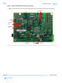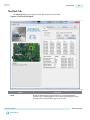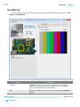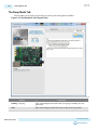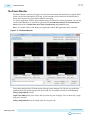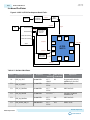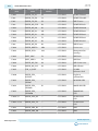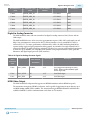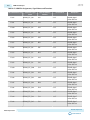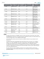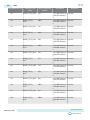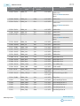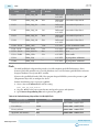
1
MAX 10 FPGA Development Kit User
Guide
Subscribe
Send Feedback
UG-01169
2015.11.06
101 Innovation Drive
San Jose, CA 95134
www.altera.com
TOC-2
Contents
Overview.............................................................................................................. 1-1
General Description.....................................................................................................................................1-2
Handling the Board..................................................................................................................................... 1-4
Getting Started.................................................................................................... 2-1
Quartus II Web Edition Software.............................................................................................................. 2-1
Installing the Development Kit..................................................................................................................2-1
Installing the USB-Blaster Driver.............................................................................................................. 2-2
Board Update Portal.................................................................................................................................... 2-2
Board Test System............................................................................................... 3-1
Using the Configure Menu......................................................................................................................... 3-3
The System Info Tab....................................................................................................................................3-5
The GPIO Tab.............................................................................................................................................. 3-7
The Flash Tab............................................................................................................................................... 3-9
The HSMC Tab.......................................................................................................................................... 3-11
The DDR3 Tab........................................................................................................................................... 3-13
The ADC Tab............................................................................................................................................. 3-15
The HDMI Tab...........................................................................................................................................3-17
The Sleep Mode Tab.................................................................................................................................. 3-18
The Power Monitor................................................................................................................................... 3-20
The Clock Control..................................................................................................................................... 3-22
Board Components..............................................................................................4-1
Board Overview............................................................................................................................................4-1
Featured Device............................................................................................................................................4-3
Configuration............................................................................................................................................... 4-4
Using the Quartus II Programmer................................................................................................ 4-4
Selecting the Internal Configuration Scheme.............................................................................. 4-4
Switch and Jumper Settings............................................................................................................ 4-5
Status Elements............................................................................................................................................ 4-7
Setup Elements............................................................................................................................................. 4-7
General User Input/Output........................................................................................................................4-8
Clock Circuitry............................................................................................................................................. 4-9
On-Board Oscillators.....................................................................................................................4-10
Off-Board Clock Input/Output....................................................................................................4-11
Components and Interfaces..................................................................................................................... 4-12
10/100/1000 Ethernet PHY...........................................................................................................4-12
Digital-to-Analog Converter........................................................................................................ 4-15
HDMI Video Output.....................................................................................................................4-15
Altera Corporation
TOC-3
HSMC.............................................................................................................................................. 4-17
Pmod Connectors.......................................................................................................................... 4-24
USB to UART................................................................................................................................. 4-25
Memory....................................................................................................................................................... 4-25
DDR3 Rev. B Board....................................................................................................................... 4-25
DDR3 Rev. C Board.......................................................................................................................4-28
Flash................................................................................................................................................. 4-30
Power Distribution System.......................................................................................................................4-32
Additional Information......................................................................................A-1
Board & User Guide Revision History.....................................................................................................A-1
Compliance and Conformity Statements................................................................................................ A-2
CE EMI Conformity Caution........................................................................................................ A-2
Altera Corporation
Overview
1
2015.11.06
UG-01169
Subscribe
Send Feedback
The MAX® 10 FPGA development board provides a hardware platform for evaluating the performance
and features of the Altera® MAX 10 device.
The development kit includes a RoHS- and CE-compliant MAX 10 FPGA Development board with the
following components:
• Featured Devices:
• MAX 10 FPGA (10M50D, dual supply, F484 package)
• Enpirion® EN2342QI 4 A PowerSoC Voltage-Mode Synchronous Step-Down Converter with
Integrated Inductor Enpirion
• EN6337QI 3 A High-Efficiency PowerSoC DC-DC Step-Down Converters with Integrated
Inductor
• Enpirion EP5358xUI 600 mA PowerSoC DC-DC Step-Down Converters with Integrated Inductor
• MAX II CPLD – EPM1270M256C4N (On-board USB-Blaster™ II)
• Programming and Configuration:
• Embedded USB-Blaster II (JTAG)
• Optional JTAG direct via 10-pin header
• Memory Devices:
• 64-Mx16 1 Gb DDR3 SDRAM with soft memory controller
• 128-Mx8 1 Gb DDR3 SDRAM with soft memory controller
• 512-Mb Quad serial peripheral interface (quad SPI) flash
• Communication Ports:
• Two Gigabit Ethernet (GbE) RJ-45 ports
•
•
•
•
• Ethernet Port A (Bottom)
• Ethernet Port B (Top)
One mini-USB2.0 UART
One high-definition multimedia interface (HDMI) video output
One universal high-speed mezzanine card (HSMC) connector
Two 12-pin Digilent Pmod™ compatible connectors
© 2015 Altera Corporation. All rights reserved. ALTERA, ARRIA, CYCLONE, ENPIRION, MAX, MEGACORE, NIOS, QUARTUS and STRATIX words and logos are
trademarks of Altera Corporation and registered in the U.S. Patent and Trademark Office and in other countries. All other words and logos identified as
trademarks or service marks are the property of their respective holders as described at www.altera.com/common/legal.html. Altera warrants performance
of its semiconductor products to current specifications in accordance with Altera's standard warranty, but reserves the right to make changes to any
products and services at any time without notice. Altera assumes no responsibility or liability arising out of the application or use of any information,
product, or service described herein except as expressly agreed to in writing by Altera. Altera customers are advised to obtain the latest version of device
specifications before relying on any published information and before placing orders for products or services.
www.altera.com
101 Innovation Drive, San Jose, CA 95134
ISO
9001:2008
Registered
1-2
UG-01169
2015.11.06
General Description
• Analog:
•
•
•
•
Two MAX 10 FPGA analog-to-digital converter (ADC) SMA inputs
2x10 ADC header
Potentiometer input to ADC
One external 16 bit digital-to-analog converter (DAC) device with SMA output
• Clocking
• 25 MHz single-ended, external oscillator clock source
• Silicon labs clock generator with programmable frequency GUI
• Mini-USB cable for on-board USB-Blaster™ II
• 2A Power Supply and cord
• Free Quartus® II Web Edition design software (download software and license from website)
• Complete documentation
• User manual, bill of materials, schematic, and board files
General Description
Figure 1-1: MAX 10 FPGA Board Components (Top)
2x10 PIN HEADER
(J20)
POT1
USB
BLASTER
(J12)
CLOCK GENERATION
CHIP
USB to UART
(J11)
JTAG HEADER
(J14)
MAX II USB-BLASTER II
CIRCUIT
HDMI CONNECTOR
(J8)
FPGA_CPU_RESET
BUTTON
PMOD
CONNECTOR
(J5)
USER
PUSH BUTTONS
SMA - ANAIN2
(J19)
USER PB3
USER PB2
USER PB1
USER PB0
SMA - ANAIN1
(J18)
PMOD
CONNECTOR
(J4)
FPGA
RECONFIGURE
BUTTON
POWER
SWITCH
(SW3)
SMA - DACOUT
(J1)
16-Bit DAC
DC INPUT
12 V
(J15)
DUAL ETHERNET
CONNECTOR
(RJ1)
Ethernet A (Bottom)
Ethernet B (Top)
LED4
LED3
LED2
LED1
LED0
USER LEDs
Altera Corporation
DDR3 64Mx16
SDRAM
Enpirion EN6337 3A
PowerSoC
Enpirion EN2342QI 4A
HSMC CONNECTOR PowerSoC
(J2)
Overview
Send Feedback
UG-01169
2015.11.06
General Description
1-3
Figure 1-2: MAX 10 FPGA Board Components (Bottom)
Note: To determine the revision of your board, look for the serial number at the bottom of the board.
QUAD SPI FLASH
ENPIRION
EN6337
USER DIP SWITCH
(SW2)
USER DIP SWITCH
(SW1)
DDR3 128Mx8
SDRAM (U6)
Overview
Send Feedback
BOARD
REVISON
ENPIRION
EN6337
Altera Corporation
1-4
UG-01169
2015.11.06
Handling the Board
Figure 1-3: System Block Diagram
DC Supply
USB Blaster
FTDI + MAXII/ V
HDMI TX
USB to UART
DDR 3
512 Mb x16
2x 1 GbE
QSPI Flash
1 Gb x16
HSMC
2x10
ADC IN/GPI O
PMOD
DACOUT
DAC
PMOD
AIN1 AIN2
Potentiometer
Qsci llator
User LEDs
~
~
FPGA _RESET
JTAG
User DIP Switches
User Push Buttons
Handling the Board
When handling the board, it is important to observe static discharge precautions.
Caution: Without proper anti-static handling, the board can be damaged. Therefore, use anti-static
handling precautions when touching the board.
Altera Corporation
Overview
Send Feedback
2
Getting Started
2015.11.06
UG-01169
Subscribe
Send Feedback
Quartus II Web Edition Software
The Quartus II Web Edition Software is a free with no license required.
You can download the Web Edition software from the Altera website. Alternatively, you can request a
DVD.
Related Information
• Quartus II Web Edition Software
• Altera IP and Software DVD Request Form
• Altera Quartus II Software - Subscription Edition vs. Web Edition
Installing the Development Kit
1. Download the MAX 10 Development Kit installer from the MAX 10 FPGA Development Kit page of
the Altera website. Alternatively, you can request a development kit DVD from the Altera Kit Installa‐
tions DVD Request Form page of the Altera website.
2. Run the MAX 10 FPGA Development Kit installer.
3. Follow the on-screen instructions to complete the installation process. Be sure that the installation
directory you choose is in the same relative location to the Quartus II software installation.
The installation program creates the development kit directory structure shown in the following figure.
Attention: .sof files are used by BTS GUI to configure the MAX 10 device and start corresponding
test. Therefore, do not to move the .sof files from the *\examples\board_test_system
directory.
© 2015 Altera Corporation. All rights reserved. ALTERA, ARRIA, CYCLONE, ENPIRION, MAX, MEGACORE, NIOS, QUARTUS and STRATIX words and logos are
trademarks of Altera Corporation and registered in the U.S. Patent and Trademark Office and in other countries. All other words and logos identified as
trademarks or service marks are the property of their respective holders as described at www.altera.com/common/legal.html. Altera warrants performance
of its semiconductor products to current specifications in accordance with Altera's standard warranty, but reserves the right to make changes to any
products and services at any time without notice. Altera assumes no responsibility or liability arising out of the application or use of any information,
product, or service described herein except as expressly agreed to in writing by Altera. Altera customers are advised to obtain the latest version of device
specifications before relying on any published information and before placing orders for products or services.
www.altera.com
101 Innovation Drive, San Jose, CA 95134
ISO
9001:2008
Registered
2-2
UG-01169
2015.11.06
Installing the USB-Blaster Driver
Figure 2-1: Installed Development Kit Directory Structure
<install dir>
The default Windows installation directory is C:\altera\<version>\.
kits
<device name>
board_design_files
demos
documents
examples
factory_recovery
Table 2-1: Installed Directory Contents
Directory Name
Description of Contents
board_design_files
Contains schematic, layout, assembly, and bill of material board design files.
Use these files as a starting point for a new prototype board design.
demos
Contains demonstration applications when available.
documents
Contains the following documentation:
• MAX 10 FPGA Development Kit User Guide
• Quick Start Guide
• Dear Customer Letter
examples
Contains the sample design files for this kit.
factory_recovery
Contains the original data programmed onto the board before shipment. Use
this data to restore the board with its original factory contents.
Installing the USB-Blaster Driver
The development board includes integrated USB-Blaster circuitry for FPGA programming. However, for
the host computer and board to communicate, you must install the On-Board USB-Blaster II driver on
the host computer.
Installation instructions for the On-Board USB-Blaster II driver for your operating system are available on
the Altera website. On the Altera Programming Cable Driver Information page of the Altera website,
locate the table entry for your configuration and click the link to access the instructions.
Board Update Portal
You can keep your board current by accessing the Board Update Portal on www.altera.com.
Altera Corporation
Getting Started
Send Feedback
UG-01169
2015.11.06
Board Update Portal
2-3
This web site allows you access useful information and updated software and design examples for your
board. For instructions on setting up your board to access the Board Update Portal, consult the printed
Quick Start Guide that is included in the kit box.
Getting Started
Send Feedback
Altera Corporation
Board Test System
3
2015.11.06
UG-01169
Subscribe
Send Feedback
This kit includes an application called the Board Test System (BTS).
The BTS provides an easy-to-use interface to alter functional settings and observe the results. You can use
the BTS to test board components, modify functional parameters, observe performance, and measure
power usage. While using the BTS, you reconfigure the FPGA several times with test designs specific to
the functionality you are testing.
© 2015 Altera Corporation. All rights reserved. ALTERA, ARRIA, CYCLONE, ENPIRION, MAX, MEGACORE, NIOS, QUARTUS and STRATIX words and logos are
trademarks of Altera Corporation and registered in the U.S. Patent and Trademark Office and in other countries. All other words and logos identified as
trademarks or service marks are the property of their respective holders as described at www.altera.com/common/legal.html. Altera warrants performance
of its semiconductor products to current specifications in accordance with Altera's standard warranty, but reserves the right to make changes to any
products and services at any time without notice. Altera assumes no responsibility or liability arising out of the application or use of any information,
product, or service described herein except as expressly agreed to in writing by Altera. Altera customers are advised to obtain the latest version of device
specifications before relying on any published information and before placing orders for products or services.
www.altera.com
101 Innovation Drive, San Jose, CA 95134
ISO
9001:2008
Registered
3-2
Board Test System
UG-01169
2015.11.06
Figure 3-1: Board Test System GUI
Several designs are provided to test the major board features. Each design provides data for one or more
tabs in the application. The Configure menu identifies the appropriate design to download to the FPGA
for each tab.
After successful FPGA configuration, the appropriate tab appears that allows you to exercise the related
board features. Highlights appear in the board picture around the corresponding components
The BTS communicates over the JTAG bus to a test design running in the FPGA. The Board Test System
and Power Monitor share the JTAG bus with other applications like the Nios II debugger and the
SignalTap® II Embedded Logic Analyzer. Because the Quartus II programmer uses most of the bandwidth
of the JTAG bus, other applications using the JTAG bus might time out. Be sure to close the other applica‐
tions before attempting to reconfigure the FPGA using the Quartus II Programmer.
Altera Corporation
Board Test System
Send Feedback
UG-01169
2015.11.06
Using the Configure Menu
3-3
Using the Configure Menu
Use the Configure menu to select the design you want to use. Each design example tests different board
features. Choose a design from this menu and the corresponding tabs become active for testing.
Figure 3-2: The Configure Menu
Board Test System
Send Feedback
Altera Corporation
3-4
Using the Configure Menu
UG-01169
2015.11.06
To configure the FPGA with a test system design, perform the following steps:
1. On the Configure menu, click the configure command that corresponds to the functionality you wish
to test.
2. In the dialog box that appears, click Configure to download the corresponding design to the FPGA.
3. When configuration finishes, close the Quartus II Programmer if open. The design begins running in
the FPGA. The corresponding GUI application tabs that interface with the design are now enabled.
If you use the Quartus II Programmer for configuration, rather than the Board Test System GUI, you may
need to restart the GUI.
Altera Corporation
Board Test System
Send Feedback
UG-01169
2015.11.06
The System Info Tab
3-5
The System Info Tab
The System Info tab shows the board’s current configuration. The tab displays the JTAG chain, the
board’s MAC address, the Qsys memory map, and other details stored on the board.
Figure 3-3: The System Info Tab
Board Test System
Send Feedback
Altera Corporation
3-6
UG-01169
2015.11.06
The System Info Tab
Table 3-1: Controls on the System Info Tab
Controls
Description
Board Information Controls
The board information is updated once the GPIO design is configured.
Otherwise, this control displays the default static information about
your board.
Board Name
Indicates the official name of the board, given by the Board Test
System.
Board P/N
Indicates the part number of the board.
Serial Number
Indicates the serial number of the board.
Factory Test Version
Indicates the version of the Board Test System currently running on
the board.
MAX Version
Indicates the version of MAX code currently running on the board.
Ethernet A MAC
Indicates the Ethernet A MAC address of the board.
Ethernet B MAC
Indicates the Ethernet B MAC address of the board.
JTAG Chain
Shows all the devices currently in the JTAG chain.
Qsys Memory Map
Shows the memory map of the Qsys system on your board.
Altera Corporation
Board Test System
Send Feedback
UG-01169
2015.11.06
The GPIO Tab
3-7
The GPIO Tab
The GPIO tab allows you to interact with all the general purpose user I/O components on your board.
You can read DIP switch settings, turn LEDs on or off, and detect push button presses.
Figure 3-4: The GPIO Tab
Table 3-2: Controls on the GPIO Tab
User DIP Switch
Board Test System
Send Feedback
Displays the current positions of the switches in the user DIP switch
banks. Change the switches on the board to see the graphical display
change accordingly.
Altera Corporation
3-8
The GPIO Tab
UG-01169
2015.11.06
User LEDs
Displays the current state of the user LEDs for the FPGA. To toggle the
board LEDs, click the 0 to 4 buttons to toggle red or green LEDs, or
click the All button.
Push Button Switches
Read-only control displays the current state of the board user push
buttons. Press a push button on the board to see the graphical display
change accordingly.
Altera Corporation
Board Test System
Send Feedback
UG-01169
2015.11.06
The Flash Tab
3-9
The Flash Tab
The Flash Tab allows you to read and write flash memory on your board.
Figure 3-5: The Flash Tab (Detail)
Control
Read
Board Test System
Send Feedback
Description
Reads the flash memory on your board. To see the flash memory
contents, type a starting address in the text box and click Read. Values
starting at the specified address appear in the table.
Altera Corporation
3-10
UG-01169
2015.11.06
The Flash Tab
Control
Description
Write
Writes the flash memory on your board. To update the flash memory
contents, change values in the table and click Write. The application
writes the new values to flash memory and then reads the values back
to guarantee that the graphical display accurately reflects the memory
contents.
Erase
Erases flash memory.
Increment Test
Starts an incrementing data pattern test to flash memory, limited to
the 512 K test system scratch page.
Random Test
Starts a random data pattern test to flash memory, limited to the 512 K
test system scratch page.
Flash Memory Map
Displays the flash memory map for the development board.
Altera Corporation
Board Test System
Send Feedback
UG-01169
2015.11.06
The HSMC Tab
3-11
The HSMC Tab
The HSMC Tab allows you to test the CMOS port.
Figure 3-6: The HSMC Tab
Control
Description
Status
Pattern sync: Shows the pattern synced or not synced state. The
pattern is considered synced when the start of the data sequence is
detected.
Port
CMOS: The CMOS port is available for tests.
Board Test System
Send Feedback
Altera Corporation
3-12
UG-01169
2015.11.06
The HSMC Tab
Control
Data Type
Description
The following data types are available for analysis:
•
•
•
•
•
•
prbs7: Selects pseudo-random 7-bit sequences.
prbs15: Selects pseudo-random 15-bit sequences.
prbs23: Selects pseudo-random 23-bit sequences.
prbs31: Selects pseudo-random 31-bit sequences.
high_frequency: Divide by data pattern.
low_frequency: Divide by data pattern.
Error Control
• Detected errors: Displays the number of data errors detected in the
hardware.
• Inserted errors: Displays the number of errors inserted into the
transmit data stream.
• Bit error rate (BER): Displays the bit error rate of the interface
• Insert Error: Inserts a one-word error into the transmit data
stream each time you click the button.
• Clear: Resets the Detected errors and Inserted errors counters to
zeroes.
Test Control
• Stop: Resets the test.
• Number of bits tested: Displays the number of bits tested since the
last reset.
Altera Corporation
Board Test System
Send Feedback
UG-01169
2015.11.06
The DDR3 Tab
3-13
The DDR3 Tab
The DDR3 Tab allows you to test the DDR3 by reading and writing to a selected amount of addresses.
Figure 3-7: The DDR3 Tab
Board Test System
Send Feedback
Altera Corporation
3-14
UG-01169
2015.11.06
The DDR3 Tab
Control
Performance Indicators
Description
These controls display current transaction performance analysis
information collected since you last clicked Start:
• Write, Read, and Total performance bars—Show the percentage of
maximum theoretical data rate that the requested transactions are
able to achieve.
• Write (MBps), Read (MBps), and Total (MBps)—Show the
number of bytes of data analyzed per second.
• Data bus: 72 bits (8 bits ECC) wide and the frequency is 1066 MHz
double data rate. 2133 Megabits per second (Mbps) per pin.
Equating to a theoretical maximum bandwidth of 136512 Mbps or
17064 MBps.
Error Control
This control displays data errors detected during analysis and allows
you to insert errors:
• Detected errors—Displays the number of data errors detected in
the hardware.
• Inserted errors—Displays the number of errors inserted into the
transaction stream.
• Insert Error—Inserts a one-word error into the transaction stream
each time you click the button. Insert Error is only enabled during
transaction performance analysis.
• Clear—Resets the Detected errors and Inserted errors counters to
zeroes.
Number of Addresses to Write
and Read
Altera Corporation
Determines the number of addresses to use in each iteration of reads
and writes.
Board Test System
Send Feedback
UG-01169
2015.11.06
The ADC Tab
3-15
The ADC Tab
The ADC Tab (analog-to-digital) shows the real-time voltage values of all of the ADC input channels.
Figure 3-8: The ADC Tab
The two tables displayed on this tab, ADC 1 and ADC 2 are not editable. The following table shows where
the channels connect to.
Dedicated Channel
SMA Connector
ADC 1
ANAIN1_SMA(J18)
Channel0
Board Test System
Send Feedback
ADC1_CH0(J20.1)
Altera Corporation
3-16
UG-01169
2015.11.06
The ADC Tab
Dedicated Channel
SMA Connector
ADC 1
ANAIN1_SMA(J18)
Channel1
ADC1_CH1(J20.3)
Channel2
ADC1_CH2(J20.5)
Channel3
ADC1_CH2(J20.7)
Channel4
ADC1_CH4(J20.11)
Channel5
ADC1_CH4(J20.13)
Channel6
ADC1_CH6(J20.15 or POT1)
Channel7
ADC1_CH7(J20.17)
Dedicated Channel
SMA Connector
ADC 2
ANAIN2_SMA(J19)
Channel0
ADC1_CH0(J20.2)
Channel1
ADC1_CH1(J20.4)
Channel2
ADC1_CH2(J20.6)
Channel3
ADC1_CH2(J20.8)
Channel4
ADC1_CH4(J20.12)
Channel5
ADC1_CH4(J20.14)
Channel6
ADC1_CH6(J20.16)
Channel7
ADC1_CH7(J20.18)
Altera Corporation
Board Test System
Send Feedback
UG-01169
2015.11.06
The HDMI Tab
3-17
The HDMI Tab
This tab displays a transmitter color bar pattern from the high-definition multimedia interface (HDMI).
Figure 3-9: The HDMI Tab
Control
Description
TX Pattern
Color Bar: Use this control to choose TX patterns. The available
choices are red, blue, green, white, and black. If you select the Start
button, the TX pattern displays immediately.
Start
When you click this button, the selected TX pattern (from Color Bar)
displays.
Board Test System
Send Feedback
Altera Corporation
3-18
UG-01169
2015.11.06
The Sleep Mode Tab
The Sleep Mode Tab
This tab allows you to test the sleep mode aspect of the power management controller.
Figure 3-10: The Sleep Mode Tab (Cropped View)
Control
Description
running (/sleeping)
This control displays the mode status as sleeping or running. It is not
interactive.
Note
This control displays board LED events related to the sleep mode.
Altera Corporation
Board Test System
Send Feedback
UG-01169
2015.11.06
The Sleep Mode Tab
3-19
Related Information
MAX 10 Power Management User Guide
Provides details on the sleep mode.
Board Test System
Send Feedback
Altera Corporation
3-20
UG-01169
2015.11.06
The Power Monitor
The Power Monitor
The Power Monitor measures and reports current power information and communicates with the MAX
II device on the board through the JTAG bus. A power monitor circuit attached to the MAX II device
allows you to measure the power that the FPGA is consuming.
To start the application, click the Power Monitor icon in the Board Test System application. You can also
run the Power Monitor as a stand-alone application. The PowerMonitor(32-bit.exe) and PowerMonitor(64bit.exe) reside in the <install dir>\kits\<device name>\examples\board_test_system directory.
Note: You cannot run the stand-alone power application and the BTS application at the same time.
Figure 3-11: The Power Monitor
This window displays both LTC2990 current and temperature monitors. The left side top and bottom
quadrant shows U29 and the opposite side shows U30. Use the available controls to show Current or
Voltage Single-Ended, or both.
Single Chart Mode allows you to choose how you want the panes to display. You can show only a single
large pane, if needed.
Voltage Single-Ended shows the voltage value of each power rail:
Altera Corporation
Board Test System
Send Feedback
UG-01169
2015.11.06
The Power Monitor
•
•
•
•
3-21
2.5 V CORE
2.5 V VCCIO
1.5 V VCCIO
1.2 VVCC
Single-ended shows the voltage of SENSE_P only.
The LT2990 also shows a differential voltage value of the sampling resistor SENSE_P and SENSE_N.
Sample Speed allows you to select Slow at 5 seconds, or Fast: at 1 second (default).
Record Log saves a comma-separated values (CSV) format file ltc2990.csv in the *\examples\board_test_
system directory.
Board Test System
Send Feedback
Altera Corporation
3-22
UG-01169
2015.11.06
The Clock Control
The Clock Control
The MAX 10 FPGA development board Clock Control application sets the programmable oscillators to
any frequency between 10 MHz and 810 MHz. The frequencies support eight digits of precision to the
right of the decimal point.
The Clock Control communicates with the MAX II device on the board through the JTAG bus. The
programmable oscillators are connected to the MAX II device through a 2-wire serial bus.
Figure 3-12: The Si570 Tab
Control
Description
Serial Port Registers
Shows the current values from the Si570 registers for frequency
configuration.
Target frequency (MHZ)
Allows you to specify the frequency of the clock. Legal values are
between 10 and 810 MHz with eight digits of precision to the right of
the decimal point. For example, 421.31259873 is possible within 100
parts per million (ppm). The Target frequency control works in
conjunction with the Set New Freq control.
fXTAL
Shows the calculated internal fixed-frequency crystal, based on the
serial port register values.
Default
Sets the frequency for the oscillator associated with the active tab back
to its default value. This can also be accomplished by power cycling the
board.
Read
Reads the current frequency setting for the oscillator associated with
the active tab.
Altera Corporation
Board Test System
Send Feedback
UG-01169
2015.11.06
The Clock Control
Control
Set New Freq
3-23
Description
Sets the programmable oscillator frequency for the selected clock to
the value in the Target frequency control for the programmable
oscillators. Frequency changes might take several milliseconds to take
effect. You might see glitches on the clock during this time. Altera
recommends resetting the FPGA logic after changing frequencies.
Figure 3-13: The Si5338 Tab
Control
Description
F_vco
Displays the generating signal value of the voltage-controlled
oscillator.
Registers
Display the current frequencies for each oscillator.
Frequency (MHz)
Allows you to specify the frequency of the clock.
Disable
Disable each oscillators as required.
Read
Reads the current frequency setting for the oscillator associated with
the active tab.
Default
Sets the frequency for the oscillator associated with the active tab back
to its default value. This can also be accomplished by power cycling the
board.
Board Test System
Send Feedback
Altera Corporation
3-24
UG-01169
2015.11.06
The Clock Control
Control
Set New Freq
Description
Sets the programmable oscillator frequency for the selected clock to
the value in the CLK0 to CLK3 controls. Frequency changes might
take several milliseconds to take effect. You might see glitches on the
clock during this time. Altera recommends resetting the FPGA logic
after changing frequencies.
Note: Changing CLK0 of Si5338 will affect the Clock/Power GUI.
One clock from port CLK0 is used to drive the MAX II
device which as a 2-wire serial bus interface connected to
SI570, Si5338, and the power monitor.
Altera Corporation
Board Test System
Send Feedback
4
Board Components
2015.11.06
UG-01169
Send Feedback
Subscribe
This chapter introduces all the important components on the development kit board.
A complete set of schematics, a physical layout database, and GERBER files for the development board
reside in the development kit documents directory.
Board Overview
This topic provides a high-level list of the major components of the MAX 10 FPGA development board.
Table 4-1: MAX 10 FPGA Board Components
Board Reference
Type
Description
Featured Devices
U1
FPGA
MAX MAX 10 FPGA
10M50DAF484C6GES, 50K LEs, F484
package.
U13
CPLD
MAX II EPM1270 256-MBGA, 2.5 V/3.3 V,
VCCINT for On-Board USB-Blaster II.
U17
Power Regulator
Enpirion® EN2342QI, PowerSoC voltagemode synchronous step-down converter
with integrated inductor.
U22, U23, U27
Power Regulator
Enpirion EN6337QI, PowerSoC DC-DC
step-down converters with integrated
inductor.
U26
Power Regulator
Enpirion EP5358LUI, 600 mA PowerSoC
DC-DC step-down converters with
integrated inductor.
U24, U25
Power Regulator
Enpirion EP5358HUI, 600 mA PowerSoC
DC-DC step-down converters with
integrated inductor.
Configuration and Setup Elements
J12
On-Board (Embedded) USBBlasterBlaster II
Type-B USB connector for programming
and debugging the FPGA.
© 2015 Altera Corporation. All rights reserved. ALTERA, ARRIA, CYCLONE, ENPIRION, MAX, MEGACORE, NIOS, QUARTUS and STRATIX words and logos are
trademarks of Altera Corporation and registered in the U.S. Patent and Trademark Office and in other countries. All other words and logos identified as
trademarks or service marks are the property of their respective holders as described at www.altera.com/common/legal.html. Altera warrants performance
of its semiconductor products to current specifications in accordance with Altera's standard warranty, but reserves the right to make changes to any
products and services at any time without notice. Altera assumes no responsibility or liability arising out of the application or use of any information,
product, or service described herein except as expressly agreed to in writing by Altera. Altera customers are advised to obtain the latest version of device
specifications before relying on any published information and before placing orders for products or services.
www.altera.com
101 Innovation Drive, San Jose, CA 95134
ISO
9001:2008
Registered
4-2
UG-01169
2015.11.06
Board Overview
Board Reference
Type
Description
J14
10-pin header
Optional JTAG direct via 10-pin header for
external download cables.
J20
2x10-pin header
16 dual-purpose ADC channels are
connected to the 2x10 header.
SW2
DIP configuration and user
switch
SW2 Includes switches to control boot
images, JTAG bypass and HSMC bypass.
J7
Jumper for the MAX 10 ADC
Connects potentiometer for providing
adjustable voltage to the ADC.
S5
Pulse_nconfig push button
Emulates pulsing the nCONFIG pin low to
trigger reconfiguration even though the
physical pin is unaffected.
S6
CPU reset push button
Default reset for the FPGA logic.
D1
Blue power LED
Illuminates when 12-V power is present.
D2
Green high-speed mezzanine
card (HSMC) LED
Illuminates when the HSMC is present.
D13, D14
Green USB-UART LEDs
Illuminates when the USB-UART
transmitter and receiver are in use.
D20
Configuration done LED
Illuminates when the FPGA is configured.
D21, D22, D23
Power LEDs
Indicates that 3.3 V, 2.5 V, 1.2 V are
powered up successfully.
Status Elements
Clock Circuitry
X1
Programmable Clock for ADC Programmable oscillator for ADC with
default frequency of 10 MHz.
U2
Programmable Clock
Four channel programmable oscillator with
default frequencies of 25, 50, 100, 125 MHz.
S1, S2, S3, S4
General user push buttons
Four user push buttons. Driven low when
pressed.
D15, D16, D17, D18, D19
User LEDs
Four user LEDs. Illuminates when driven
low.
SW1, SW2.1
User DIP switches
Quad user DIP switches.
U5
DDR3 SDRAM A memory
64 Mx16.
U6
DDR3 SDRAM B memory
128 Mx8.
U7
Quad serial peripheral
interface (quad SPI) flash
512 Mb.
General User Input/Output
Memory Devices
Communication Ports
Altera Corporation
Board Components
Send Feedback
UG-01169
2015.11.06
Featured Device
Board Reference
Type
4-3
Description
J2
HSMC port
Provides 84 CMOS or 17 LVDS channels
per HSMC specification.
U9, U10
Two Gigabit Ethernet ports
RJ-45 connector which provides a 10/100/
1000 Ethernet connection via a Marvell
88E1111 x 2 PHY and the FPGA-based
Altera Triple Speed Ethernet MegaCore
function in RGMII mode.
• Ethernet A (Bottom)
• Ethernet B (Top)
J4, J5
Two Diligent Pmod
connectors
12-pin interface with 8 I/O signal pins used
to connect low frequency, low I/O
peripheral modules.
J11
Mini-USB 2.0 UART port
USB connector with USB-to-UART bridge
for serial UART interface
J12
Mini-USB port
Embedded USB-Blaster II.
J18, J19
SMA inputs
Two FPGA analog-to-digital converter
(ADC).
J20
Header
2x10 ADC.
POT1
Potentiometer
Input to ADC.
J1
SMA output
External 16 bit digital-to-analog converter
(DAC) device.
HDMI video output
19-pin HDMI connector which provides a
HDMI v1.4 video output of up to 1080p
through an ADI (Analog Devices, Inc)
PHY.
J15
DC input jack
Accepts 12 V DC power supply.
SW3
Power switch
Switch to power on or off the board when
power is supplied from the DC input jack.
Analog
Video and Display Ports
U8
Power Supply
Featured Device
The MAX 10 FPGA development board features the MAX 10 10M50DAF484C6GES device (U1) in a 484pin FineLine BGA package.
Table 4-2: MAX 10 FPGA 10M50DAF484C6GES Features
ALMs
50,000
Equivalent
LEs
50
Board Components
Send Feedback
M9K
Memory
(Kb)
1,638
Total RAM
(Kb)
736
18-bit x 18bit
Multipliers
144
PLLs
4
Transceivers
—
Package Type
FineLine BGA
484 pins
Altera Corporation
4-4
UG-01169
2015.11.06
Configuration
Configuration
The MAX 10 FPGA development kit supports two configuration methods:
• Configuration by downloading a .sof file to the FPGA. Any power cycling of the FPGA or reconfigura‐
tion will power up the FPGA to a blank state.
• Programming of the on-die FPGA Configuration Flash Memory (CFM) via a .pof file. Any power
cycling of the FPGA or reconfiguration will power up the FPGA in self-configuration mode, using the
files stored in the CFM.
You can use two different USB-Blaster™ hardware components to program the .sof or .pof files:
• Embedded USB-Blaster II, type-B connector (J12).
• JTAG header (J14). Use an external USB-Blaster, USB-Blaster II, or Ethernet Blaster download cable.
The external download cable connects to the board through the JTAG header (J14).
Using the Quartus II Programmer
You can use the Quartus II Programmer to configure the FPGA with a .sof.
Before configuring the FPGA:
• Ensure that the Quartus II Programmer and the USB-Blaster driver are installed on the host computer
• The USB cable is connected to the kit
• Power to the board is on, and no other applications that use the JTAG chain are running
To configure the MAX 10 FPGA:
1.
2.
3.
4.
Start the Quartus II Programmer.
Click Add File and select the path to the desired .sof.
Turn on the Program/Configure option for the added file.
Click Start to download the selected file to the FPGA. Configuration is complete when the progress
bar reaches 100%.
The Quartus II Convert Programming File (CPF) GUI can be used to generate a .sof file that can use for
internal configuration. You can directly program the MAX 10 device’s flash which included
Configuration Flash Memory (CFM) and User Flash Memory (UFM) by using a download cable with the
Quartus II software programmer.
Selecting the Internal Configuration Scheme
For all MAX 10 devices, except 10M02 device, there are total of 5 different modes you can select internal
configuration.
The internal configuration scheme needs to be selected before design compilation.
To select the configuration mode:
1.
2.
3.
4.
5.
Altera Corporation
Open the Quartus II software and load a project using MAX 10 device family.
On the Assignments menu, click Settings. The Settings dialog box appears.
In the Category list, select Device. The Device page appears.
Click Device and Pin Options.
In the Device and Pin Options dialog box, click the Configuration tab.
Board Components
Send Feedback
UG-01169
2015.11.06
Switch and Jumper Settings
4-5
6. In the Configuration Scheme list, select Internal Configuration.
7. In the Configuration Mode list, select 1 out of 5 configuration modes. For the dual-boot feature:
a. Must have a Dual Boot IP core in the design, for example, in a Qsys component.
b. Choose Dual Compressed Images (512 Kbits UFM) for the Configuration Mode.
c. Generate two sof files above and convert them into one POF file for CFM programming.
8. Turn on Generate compressed bitstreams if needed, and click OK.
Switch and Jumper Settings
This topic is for the MAX 10 FPGA development kit. This topic shows you how to restore the default
factory settings and explains their functions.
The J7 jumper connects the output of potentiometer (POT1.2) to ADC1_CH6. When J7 jumper is on, you
can use the potentiometer to provide adjustable voltage (0~2.5 V) to the MAX 10 ADC through
ADC1_CH6. When J7 jumper is off, ADC1_CH6 is connected to the 2x10 header as the other ADC
channels.
Figure 4-1: Jumper J7 on the Top of the Board (Detail)
POT1
ANAIN2
ANAIN1
J7
DACOUT
There are two switches on the bottom of the board. SW1 is for user functions, and SW2 allows for booting
selection and bypassing some components.
Board Components
Send Feedback
Altera Corporation
4-6
UG-01169
2015.11.06
Switch and Jumper Settings
Figure 4-2: Switches on the Bottom Board (Detail)
When a switch is ON, it means the FUNCTION SIGNAL is connected to GND. So it is a LOGIC LOW
(0). When switch is OFF, it means the FUNCTION SIGNAL is disconnected from GND. So it is a LOGIC
HIGH (1).
Note: The following figure shows the switch labels for the Rev. C board and a note for the Rev. B board.
The change of name for SW2.3 is just a name change, not a functional change. Rev. B is labeled
MAX10_BYPASS, but it is actually a VTAP bypass.
USER_DIPSW4
CONFIG_SEL
VTAP_BYPASSN
HSMC_BYPASSN
4 3 2 1
For Rev. B:
2 = BOOT_SEL
3 = MAX10_BYPASSN
OFF = 1
SW2
ON = 0
1 2 3 4
ON = 0
SW1
OFF = 1
Table 4-3: SW2 DIP Switch Settings (Board Bottom)
Switch
Board Label
Function
1
USER_DIPSW4
2
BOOT_SEL (for Rev. Use this pin to choose CFM0, CFM1 or CFM2
B Board)
image as the first boot image in dual-image
configuration. If the CONFIG_SEL is set to low,
the first boot image is CFM0 image. If the
CONFIG_SEL (for
CONFIG_SEL pin is set to high, the first boot
Rev. C board)
image is CFM1 or CFM2 image. This pin is read
before user mode and before the nSTATUS pin is
asserted.
Altera Corporation
User defined switch #4, #0/1/2/3 is on SW1. No
default function.
Default Position
—
LOW
Board Components
Send Feedback
UG-01169
2015.11.06
Status Elements
Switch
Board Label
Function
4-7
Default Position
3
VTAP_BYPASSN
A virtual JTAG device is provided within the On- HIGH
Board USB-Blaster II, it provides access to
diagnostic hardware and board identification
information. The device shows up as an extra
device on the JTAG chain with ID: 020D10DD.
This switch removes the virtual JTAG device from
the JTAG chain.
4
HSMC_BYPASSN
Use this pin to bypass HSMC from JTAG chain.
HIGH
The default value of this signal is high so HSMC is
in the JTAG chain. (However, there is no
daughter cards connected to HSMC normally so it
would not be detected by JTAG master). When it
is set to low, HSMC is bypassed.
Status Elements
This topic lists the non-user status elements for the MAX 10 FPGA development board.
Table 4-4: General LED Signal Names
Board Reference
Signal Name
Description
D1
—
Blue Power LED
D2
HSMC_PRSNTn
Green LED
D13
UART_TXLED
Green LED for USB to UART
D14
UART_RXLED
Green LED for USB to UART
Table 4-5: MAX II CPLD LED Signal Names
Board Reference
Signal Name
I/O Standard
MAX II CPLD Pin Number
D20
MAXII_CONF_DONE
3.3 V
W17
D21
3.3V_LED
3.3 V
U4
D22
2.5V_LED
3.3 V
U5
D23
1.2V_LED
3.3 V
U6
Setup Elements
Table 4-6: Board Settings DIP Switch and Jumper Schematic Signals
Board Reference
SW2.1
Board Components
Send Feedback
Signal Name
USER_DIPSW4
Device / Pin Number
MAX 10 / H21
I/O Standard
1.5 V
Altera Corporation
4-8
UG-01169
2015.11.06
General User Input/Output
Board Reference
Signal Name
Device / Pin Number
I/O Standard
SW2.2
CONFIG_SEL
MAX 10 / H10
3.3 V
SW2.3
VTAP_BYPASSN
MAX II / P17
3.3 V
SW2.4
HSMC_BYPASSn
MAX II / P18
3.3 V
J7.1
—
POT1
2.5 V
J7.2
ADC1_CH6
2x10 Header / J20.15
2.5 V
Table 4-7: General Push Button Signal Names
Board Reference
Signal Name
MAX 10 FPGA Pin
Number
I/O Standard
S5
PULSE_NCONFIG
H9
3.3 V
S6
CPU_RESETn
D9
3.3 V
General User Input/Output
User-defined I/O signal names, FPGA pin numbers, and I/O standards for the MAX 10 FPGA
development board.
Table 4-8: User-Defined Push Button Signal Names
Board Reference
Signal Name
I/O Standard
MAX 10 FPGA
Pin Number
S1
USER_PB0
L22
1.5 V
S2
USER_PB1
M21
1.5 V
S3
USER_PB2
M22
1.5 V
S4
USER_PB3
N21
1.5 V
Table 4-9: User-Defined DIP Switch Schematic Signal Names
Board Reference
Signal Name
I/O Standard
MAX 10 FPGA
Pin Number
SW1.1
USER_DIPSW0
H21
1.5 V
SW1.2
USER_DIPSW1
H22
1.5 V
SW1.3
USER_DIPSW2
J21
1.5 V
SW1.4
USER_DIPSW3
J22
1.5 V
SW2.1
USER_DIPSW4
G19
1.5 V
Altera Corporation
Board Components
Send Feedback
UG-01169
2015.11.06
Clock Circuitry
4-9
Table 4-10: User LED (Green) Schematic Signal Names
Board Reference
Signal Name
I/O Standard
MAX 10 FPGA
Pin Number
D15
USER_LED0
T20
1.5 V
D16
USER_LED1
U22
1.5 V
D17
USER_LED2
U21
1.5 V
D18
USER_LED3
AA21
1.5 V
D19
USER_LED4
AA22
1.5 V
For a MAX 10 Development Kit Baseline Pinout design vist the Altera Design Store.
Related Information
Altera Design Store (MAX 10 Development Kit)
Clock Circuitry
The development board includes a four channel programmable oscillator with default frequency of 25MHz, 50-MHz, 100-MHz, 125-MHz. The board also includes a 10-MHz programmble oscillator
connected to the ADC.
Board Components
Send Feedback
Altera Corporation
4-10
UG-01169
2015.11.06
On-Board Oscillators
On-Board Oscillators
Figure 4-3: MAX 10 FPGA Development Board Clocks
FA‐128
24MHz XTAL
8Y‐25MHz
XTAL
IN
Cypress
CY7C68013A
USB Controller
USB_CLK
MAX II
USB Blaster
50M_MAXII
USB_CLK
Default 50 MHz CH0
25M_ENET
Default 25 MHz CH1
10/100/1000 Base – T
Ethernet PHY
88E1111 x 2
Default LVDS125 MHz CH2
Bank 8
Default LVDS100 MHz CH3
50M_MAX10
Bank 7
Bank 1A
100M_DDR3
Si5338
Bank 6
Bank 1B
ALTERA
MAX 10
Bank 5
25M_MAX10
Bank 2
Si 570
CMOS ClockOutput
Default 10MHz
ADC
Bank 3
Bank 4
125M_LVDS
Table 4-11: On-Board Oscillators
Source
Schematic Signal Name
Frequency
I/O
Standard
MAX 10 FPGA
Pin Number
Application
X1
CLK_10_ADC
10.000 MHz
2.5 V
CMOS
N5
Programmable default
10MHz clock for ADC
U2
CLK_25_ENET
25.000 MHz
2.5 V
LVDS
-
Ethernet clock
U2
CLK_25_MAX10
25.000 MHz
2.5 V
LVDS
M8
MAX 10 clock
U2
CLK_50_MAXII
25.000 MHz
2.5 LVDS -
Clock for On-Board
USB Blaster II
U2
CLK_50_MAX10
50.000 MHz
2.5 V
LVDS
M9
MAX 10 clock
U2
CLK_DDR3_100_N
100.000 MHz
2.5 V
LVDS
N15
DDR3 clocks
Altera Corporation
Board Components
Send Feedback
UG-01169
2015.11.06
Off-Board Clock Input/Output
Source
Schematic Signal Name
Frequency
I/O
Standard
MAX 10 FPGA
Pin Number
4-11
Application
U2
CLK_DDR3_100_P
100.000 MHz
2.5 V
LVDS
N14
DDR3 clocks
U2
CLK_LVDS_125_N
125.000 MHz
2.5 V
LVDS
R11
LVDS clocks
U2
CLK_LVDS_125_P
125.000 MHz
2.5 V
LVDS
P11
LVDS clocks
Off-Board Clock Input/Output
The development board has input and output clocks which can be driven onto the board. The output
clocks can be programmed to different levels and I/O standards according to the FPGA device’s specifica‐
tion.
Table 4-12: Off-Board Clock Inputs
Source
Schematic Signal Name
I/O Standard
MAX 10
FPGA Pin
Number
Description
HSMC
HSMC_CLK_IN_N1
2.5 V
AB21
LVDS input from the
installed HSMC cable or
board.
HSMC
HSMC_CLK_IN_P1
2.5 V
AA20
LVDS input from the
installed HSMC cable or
board.
HSMC
HSMC_CLK_IN_N2
2.5 V
V9
LVDS input from the
installed HSMC cable or
board.
HSMC
HSMC_CLK_IN_P2
2.5 V
V10
LVDS input from the
installed HSMC cable or
board.
HSMC
HSMC_CLK_IN0
2.5 V
N4
Single-ended input from
the installed HSMC cable
or board.
Table 4-13: Off-Board Clock Outputs
Source
Schematic Signal Name
I/O Standard
MAX 10 FPGA Pin
Number
Description
HSMC
HSMC_CLK_OUT_N1
2.5 V
R13
LVDS output.
HSMC
HSMC_CLK_OUT_P1
2.5 V
P13
LVDS output.
HSMC
HSMC_CLK_OUT_N2
2.5 V
V14
LVDS output.
HSMC
HSMC_CLK_OUT_P2
2.5 V
W15
LVDS output.
Board Components
Send Feedback
Altera Corporation
4-12
UG-01169
2015.11.06
Components and Interfaces
Source
HSMC
Schematic Signal Name
I/O Standard
HSMC_CLK_OUT0
2.5 V
MAX 10 FPGA Pin
Number
AA13
Description
FPGA CMOS output
(or GPIO)
Components and Interfaces
This section describes the development board's communication ports and interface cards relative to the
MAX 10 FPGA device.
10/100/1000 Ethernet PHY
The MAX 10 FFPGA development kit supports 10/100/1000 base-T Ethernet using an external Marvell
88E1111 PHY and Altera Triple-Speed Ethernet MegaCore MAC function.
Table 4-14: Ethernet PHY A Pin Assignments, Signal Names and Functions
Board Reference
(U9)
Schematic Signal
Name
Max 10 FPGA Pin
Number
I/O Standard
Description
U9.8
ENETA_GTX_CLK
T5
2.5V CMOS
125 MHz RGMII TX
clock
U9.4
ENETA_TX_CLK
E10
3.3V LVCMOS
25/2.5 MHz MII TX
clock
U9.11
ENETA_TX_D0
R5
2.5V CMOS
RGMII TX data 0
U9.12
ENETA_TX_D1
T1
2.5V CMOS
RGMII TX data 1
U9.14
ENETA_TX_D2
W1
2.5V CMOS
RGMII TX data 2
U9.16
ENETA_TX_D3
W2
2.5V CMOS
RGMII TX data 3
U9.9
ENETA_TX_EN
R4
2.5V CMOS
RGMII TX enable
U9.7
ENETA_TX_ER
P4
2.5V CMOS
MII TX error
U9.2
ENETA_RX_CLK
P3
2.5V CMOS
RGMII RX clock
U9.95
ENETA_RX_D0
N9
2.5V CMOS
RGMII RX data 0
U9.92
ENETA_RX_D1
T1
2.5V CMOS
RGMII RX data 1
U9.93
ENETA_RX_D2
N1
2.5V CMOS
RGMII RX data 2
U9.91
ENETA_RX_D3
T3
2.5V CMOS
RGMII RX data 3
U9.94
ENETA_RX_DV
T2
2.5V CMOS
RGMII RX valid
U9.3
ENETA_RX_ER
P4
2.5V CMOS
MII RX error
U9.28
ENETA_RESETN
V8
2.5V CMOS
Device reset
U9.23
ENETA_INTn
V7
2.5V CMOS
Management bus
interrupt
Altera Corporation
Board Components
Send Feedback
UG-01169
2015.11.06
10/100/1000 Ethernet PHY
Board Reference
(U9)
Schematic Signal
Name
Max 10 FPGA Pin
Number
I/O Standard
4-13
Description
U9.25
ENET_MDC
Y6
2.5V CMOS
MDI clock
U9.24
ENETA_MDIO
Y5
2.5V CMOS
MDI data
U9.84
ENETA_RX_CRS
N8
2.5V CMOS
MII Carrier Sense
U9.83
ENETA_RX_COL
P1
2.5V CMOS
MII Collision
U9.55
CLK_25_ENET
—
2.5V CMOS
25 MHz Reference clock
U9.70
ENETA_LED_
DUPLEX
—
2.5 V CMOS
Duplex or collision LED
U9.76
ENETA_LED_
LINK10
—
2.5 V CMOS
10 Mb link LED
U9.74
ENETA_LED_
LINK100
R9
2.5V CMOS
100 Mb link LED
U9.73
ENETA_LED_
LINK1000
—
2.5V CMOS
1000 Mb link LED
U9.58, 69
ENETA_LED_RX
—
2.5V CMOS
RX data active LED
U9.61, 68
ENETA_LED_TX
—
2.5V CMOS
TX data active LED
U9.29
ENETA_MDI_P0
—
2.5V CMOS
MDI
U9.31
ENETA_MDI_N0
—
2.5V CMOS
MDI
U9.33
ENETA_MDI_P1
—
2.5V CMOS
MDI
U9.34
ENETA_MDI_N1
—
2.5V CMOS
MDI
U9.39
ENETA_MDI_P2
—
2.5V CMOS
MDI
U9.41
ENETA_MDI_N2
—
2.5V CMOS
MDI
U9.42
ENETA_MDI_P3
—
2.5V CMOS
MDI
U9.43
ENETA_MDI_N3
—
2.5V CMOS
MDI
Table 4-15: Ethernet PHY B Pin Assignments, Signal Names and Functions
Board Reference
(U10)
Schematic Signal
Name
Max 10 FPGA Pin
Number
I/O Standard
Description
U10.8
ENETB_GTX_CLK
T6
2.5V CMOS
125 MHz RGMII
TX clock
U10.4
ENETB_TX_CLK
E11
3.3V LVCMOS
25/2.5 MHz MII
TX clock
U10.11
ENETB_TX_D0
U1
2.5V CMOS
RGMII TX data 0
U10.12
ENETB_TX_D1
V1
2.5V CMOS
RGMII TX data 1
U10.14
ENETB_TX_D2
W1
2.5V CMOS
RGMII TX data 2
Board Components
Send Feedback
Altera Corporation
4-14
UG-01169
2015.11.06
10/100/1000 Ethernet PHY
Board Reference
(U10)
Schematic Signal
Name
Max 10 FPGA Pin
Number
I/O Standard
Description
U10.16
ENETB_TX_D3
U4
2.5V CMOS
RGMII TX data 3
U10.9
ENETB_TX_EN
V3
2.5V CMOS
RGMII TX enable
U10.7
ENETB_TX_ER
U5
2.5V CMOS
MII TX error
U10.2
ENETB_RX_CLK
R3
2.5V CMOS
RGMII RX clock
U10.95
ENETB_RX_D0
P8
2.5V CMOS
RGMII RX data 0
U10.92
ENETB_RX_D1
M1
2.5V CMOS
RGMII RX data 1
U10.93
ENETB_RX_D2
M2
2.5V CMOS
RGMII RX data 2
U10.91
ENETB_RX_D3
T3
2.5V CMOS
RGMII RX data 3
U10.94
ENETB_RX_DV
R1
2.5V CMOS
RGMII RX valid
U10.3
ENETB_RX_ER
R2
2.5V CMOS
MII RX error
U10.28
ENETB_RESETn
AB4
2.5V CMOS
Device reset
U10.23
ENETB_INTn
AA3
2.5V CMOS
Management bus
interrupt
U10.25
ENET_MDC
Y6
2.5V CMOS
MDI clock
U10.24
ENET_MDIO
Y5
2.5V CMOS
MDI data
U10.84
ENETB_RX_CRS
N3
2.5V CMOS
MII Carrier Sense
U10.83
ENETB_RX_COL
N2
2.5V CMOS
MII Collision
U10.55
CLK_25_ENET
—
2.5V CMOS
25 MHz
Reference clock
U10.70
ENETB_LED_
DUPLEX
—
2.5V CMOS
Duplex or
collision LED
U10.76
ENETB_LED_
LINK10
—
2.5V CMOS
10 Mb link LED
U10.74
ENETB_LED_
LINK100
P9
2.5V CMOS
100 Mb link LED
U10.73
ENETB_LED_
LINK1000
—
2.5V CMOS
1000 Mb link
LED
U10.58, 69
ENETB_LED_RX
—
2.5V CMOS
RX data active
LED
U10.61, 65, 68
ENETB_LED_TX
—
2.5V CMOS
TX data active
LED
U10.29
ENETB_MDI_P0
—
2.5V CMOS
MDI
U10.31
ENETB_MDI_N0
—
2.5V CMOS
MDI
Altera Corporation
Board Components
Send Feedback
UG-01169
2015.11.06
Digital-to-Analog Converter
Board Reference
(U10)
Schematic Signal
Name
Max 10 FPGA Pin
Number
I/O Standard
4-15
Description
U10.33
ENETB_MDI_P1
—
2.5V CMOS
MDI
U10.34
ENETB_MDI_N1
—
2.5V CMOS
MDI
U10.39
ENETB_MDI_P2
—
2.5V CMOS
MDI
U10.41
ENETB_MDI_N2
—
2.5V CMOS
MDI
U10.42
ENETB_MDI_P3
—
2.5V CMOS
MDI
U10.43
ENETB_MDI_N3
—
2.5V CMOS
MDI
Digital-to-Analog Converter
The MAX 10 FPGA comes wtih one external 16 bit digital-to-analog converter (DAC) device with an
SMA output.
The MAX 10 FPGA has two 12-bit successive approximation register (SAR) ADCs with sample rate of 1
MSps. One potentiometer is connected to ADC1_CH6 to function as a user-controlled DC, and it is
connected to 2.5 V. To ensure performance evaluation of the ADCs, the MAX 10 development kit has
separate analog supply and split partition for analog ground. An external 16-bit single channel DAC is
connected to Bank 7 to enable closed loop evaluation. The DAC uses a 3-wire serial interface that operates
at clock rates up to 30 MHz. It is compatible with standard serial perifpheral interface (SPI), quad SPI,
Microwire, and digital signal processor (DSP) interfaces.
Table 4-16: Digital-to-Analog Converter Signals
Signal Name
Board
Reference
MAX 10 FPGA
I/O Standard
Description
Pin Number
(U33)
U33.5
DAC_SYNC
U1.B10
3.3 V
Level-triggered control input (active
LOW). Frame synchronization signal
for the input data.
U33.6
DAC_SCLK
A7
3.3 V
Serial clock input
U33.7
DAC_DIN
A8
3.3 V
Serial data input
HDMI Video Output
The MAX 10 FPGA development kit supports one HDMI transmitter and one HDMI receptacle.
The transmitter incorporates HDMI v1.4 features, and is capable of supporting an input data rate up to
165 MHz (1080p @60Hz, UXGA @60Hz). The connection between HDMI transmitter and MAX 10 is
established in Bank 7, and the communication can be done via I2C interface.
Board Components
Send Feedback
Altera Corporation
4-16
UG-01169
2015.11.06
HDMI Video Output
Table 4-17: HDMI Pin Assignments, Signal Names and Functions
Board Reference (U8)
Schematic Signal
Name
Max 10 FPGA Pin
Number
I/O Standard
Description
U8.62
HDMI_TX_D0
A17
3.3 V
HDMI digital
video data bus
U8.61
HDMI_TX_D1
A18
3.3 V
HDMI digital
video data bus
U8.60
HDMI_TX_D2
A12
3.3 V
HDMI digital
video data bus
U8.59
HDMI_TX_D3
F16
3.3 V
HDMI digital
video data bus
U8.58
HDMI_TX_D4
A16
3.3 V
HDMI digital
video data bus
U8.57
HDMI_TX_D5
B12
3.3 V
HDMI digital
video data bus
U8.56
HDMI_TX_D6
F15
3.3 V
HDMI digital
video data bus
U8.55
HDMI_TX_D7
B11
3.3 V
HDMI digital
video data bus
U8.54
HDMI_TX_D8
A13
3.3 V
HDMI digital
video data bus
U8.52
HDMI_TX_D9
C15
3.3 V
HDMI digital
video data bus
U8.50
HDMI_TX_D10
C11
3.3 V
HDMI digital
video data bus
U8.49
HDMI_TX_D11
A11
3.3 V
HDMI digital
video data bus
U8.48
HDMI_TX_D12
A20
3.3 V
HDMI digital
video data bus
U8.47
HDMI_TX_D13
H13
3.3 V
HDMI digital
video data bus
U8.46
HDMI_TX_D14
E14
3.3 V
HDMI digital
video data bus
U8.45
HDMI_TX_D15
D12
3.3 V
HDMI digital
video data bus
U8.44
HDMI_TX_D16
C12
3.3 V
HDMI digital
video data bus
U8.43
HDMI_TX_D17
C19
3.3 V
HDMI digital
video data bus
Altera Corporation
Board Components
Send Feedback
UG-01169
2015.11.06
HSMC
Board Reference (U8)
Schematic Signal
Name
Max 10 FPGA Pin
Number
I/O Standard
4-17
Description
U8.42
HDMI_TX_D18
C18
3.3 V
HDMI digital
video data bus
U8.41
HDMI_TX_D19
B19
3.3 V
HDMI digital
video data bus
U8.40
HDMI_TX_D20
B17
3.3 V
HDMI digital
video data bus
U8.39
HDMI_TX_D21
B16
3.3 V
HDMI digital
video data bus
U8.38
HDMI_TX_D22
C16
3.3 V
HDMI digital
video data bus
U8.37
HDMI_TX_D23
A15
3.3 V
HDMI digital
video data bus
U8.53
HDMI_TX_CLK
D6
3.3 V
Video clock
U8.63
HDMI_TX_DE
C10
3.3 V
Video data enable
U8.64
HDMI_TX_HS
A19
3.3 V
Vertical Synchro‐
nization
U8.2
HDMI_TX_VS
J12
3.3 V
Horizontal
Synchronization
U8.28
HDMI_TX_INT
D15
3.3 V
Interrupt Signal
U8.35
HDMI_SCL
A10
3.3 V
HDMI I2C clock
U8.36
HDMI_SDA
B15
3.3 V
HDMI I2C data
HSMC
The high-speed mezzanine card (HSMC) interface is based on the Samtec 0.5 mm pitch, surface-mount
QTH/QSH family of connectors. It is designed to support a full SPI-4.2 interface (17 LVDS channels) and
3 input and output clocks as well as SMBus and JTAG signals.
Since MAX 10 does not have transceiver channels, the HSMC clock-data-recovery channels are left
unconnected.
The HSMC interface has programmable bi-directional I/O pins that can be used as 2.5-V LVCMOS,
which is 3.3-V LVTTL-compatible. These pins can also be used as various differential I/O standards
including, but not limited to, LVDS, mini-LVDS, and RSDS with up to 17 full-duplex channels.
As noted in the High Speed Mezzanine Card (HSMC) Specification manual, LVDS and single-ended I/O
standards are only guaranteed to function when mixed according to either the generic single-ended pinout or generic differential pin-out.
For more information about the HSMC specification such as signaling standards, signal integrity,
compatible connectors, and mechanical information, refer to the High Speed Mezzanine Card (HSMC)
Specification manual.
Board Components
Send Feedback
Altera Corporation
4-18
UG-01169
2015.11.06
HSMC
Table 4-18: HSMC Schematic Signals
Board Reference (J2)
Schematic Signal
Name
MAX 10 / MAX II Pin
Number
I/O Standard
Description
33
HSMC_SDA
AA19
2.5V CMOS inout
Management
serial data line
34
HSMC_SCL
Y18
2.5V CMOS out
Management
serial clock line
35
HSMC_JTAG_TCK
A9 (MAX II)
part of chain
JTAG clock
36
HSMC_JTAG_TMS
A8 (MAX II)
part of chain
JTAG mode
select
37
HSMC_JTAG_TDO A7 (MAX II)
part of chain
JTAG data out
38
HSMC_JTAG_TDI
part of chain
JTAG data in
39
HSMC_CLK_OUT0 AA13
2.5V CMOS clock
output
clock output 0
40
HSMC_CLK_IN0
N4
2.5V CMOS clock in Clock input 0
41
HSMC_D0
Y7
2.5v CMOS inout
Data bus
42
HSMC_D1
Y8
2.5v CMOS inout
Data bus
43
HSMC_D2
AB2
2.5v CMOS inout
Data bus
44
HSMC_D3
AB3
2.5v CMOS inout
Data bus
47
HSMC_TX_D_P0
W3
2.5v CMOS inout or
LVDS TX channelsp
Data bus
48
HSMC_RX_D_P0(1)
V5
2.5V CMOS inout or Data bus
LVDS RX channelsp
49
HSMC_TX_D_N0
W4
2.5V CMOS inout or Data bus
LVDS TX channelsn
50
HSMC_RX_D_N0(1) V4
2.5V CMOS inout or Data bus
LVDS RX channelsn
53
HSMC_TX_D_P1
U7
2.5v CMOS inout or
LVDS TX channelsp
54
HSMC_RX_D_P1(1)
Y2
2.5V CMOS inout or Data bus
LVDS RX channelsp
55
HSMC_TX_D_N1
U6
2.5V CMOS inout or Data bus
LVDS TX channelsn
Altera Corporation
A6 (MAX II)
Data bus
Board Components
Send Feedback
UG-01169
2015.11.06
HSMC
Board Reference (J2)
Schematic Signal
Name
MAX 10 / MAX II Pin
Number
I/O Standard
Description
56
HSMC_RX_D_N1(1) Y1
2.5V CMOS inout or Data bus
LVDS RX channelsn
59
HSMC_TX_D_P2
W6
2.5v CMOS inout or
LVDS TX channelsp
60
HSMC_RX_D_P2(1)
AA20
2.5V CMOS inout or Data bus
LVDS RX channelsp
61
HSMC_TX_D_N2
W5
2.5V CMOS inout or Data bus
LVDS TX channelsn
62
HSMC_RX_D_N2(1) AA1
2.5V CMOS inout or Data bus
LVDS RX channelsn
65
HSMC_TX_D_P3
W8
2.5v CMOS inout or
LVDS TX channelsp
66
HSMC_RX_D_P3(1)
AB8
2.5V CMOS inout or Data bus
LVDS RX channelsp
67
HSMC_TX_D_N3
W7
2.5V CMOS inout or Data bus
LVDS TX channelsn
68
HSMC_RX_D_N3(1) AA8
2.5V CMOS inout or Data bus
LVDS RX channelsn
71
HSMC_TX_D_P4
AA10
2.5v CMOS inout or
LVDS TX channelsp
72
HSMC_RX_D_P4(1)
AB9
2.5V CMOS inout or Data bus
LVDS RX channelsp
73
HSMC_TX_D_N4
Y10
2.5V CMOS inout or Data bus
LVDS TX channelsn
74
HSMC_RX_D_N4(1) AA9
2.5V CMOS inout or Data bus
LVDS RX channelsn
77
HSMC_TX_D_P5
2.5v CMOS inout or
LVDS TX channelsp
Board Components
Send Feedback
AA7
4-19
Data bus
Data bus
Data bus
Data bus
Altera Corporation
4-20
UG-01169
2015.11.06
HSMC
Board Reference (J2)
Schematic Signal
Name
MAX 10 / MAX II Pin
Number
I/O Standard
Description
78
HSMC_RX_D_P5(1)
AB7
2.5V CMOS inout or Data bus
LVDS RX channelsp
79
HSMC_TX_D_N5
AA6
2.5V CMOS inout or Data bus
LVDS TX channelsn
80
HSMC_RX_D_N5(1) AB6
2.5V CMOS inout or Data bus
LVDS RX channelsn
83
HSMC_TX_D_P6
P10
2.5v CMOS inout or
LVDS TX channelsp
84
HSMC_RX_D_P6(1)
Y4
2.5V CMOS inout or Data bus
LVDS RX channelsp
85
HSMC_TX_D_N6
R10
2.5V CMOS inout or Data bus
LVDS TX channelsn
86
HSMC_RX_D_N6(1) Y3
2.5V CMOS inout or Data bus
LVDS RX channelsn
89
HSMC_TX_D_P7
W10
2.5v CMOS inout or
LVDS TX channelsp
90
HSMC_RX_D_P7(1)
AB5
2.5V CMOS inout or Data bus
LVDS RX channelsp
91
HSMC_TX_D_N7
W9
2.5V CMOS inout or Data bus
LVDS TX channelsn
92
HSMC_RX_D_N7(1) AA5
2.5V CMOS inout or Data bus
LVDS RX channelsn
95
HSMC_CLK_OUT_ P13
P1
2.5V CMOS inout or Clock output 1
LVDS clock out
96
HSMC_CLK_IN_P1 AA20
2.5V CMOS inout or Clock input 1
LVDS clock in
97
HSMC_CLK_OUT_ R13
N1
2.5V CMOS inout or Clock output 1
LVDS clock out
98
HSMC_CLK_IN_N1 AB21
2.5V CMOS inout or Clock input 1
LVDS clock in
Altera Corporation
Data bus
Data bus
Board Components
Send Feedback
UG-01169
2015.11.06
HSMC
Board Reference (J2)
Schematic Signal
Name
MAX 10 / MAX II Pin
Number
I/O Standard
Description
101
HSMC_TX_D_P8
W14
2.5v CMOS inout or
LVDS TX channelsp
102
HSMC_RX_D_P8(1)
W13
2.5V CMOS inout or Data bus
LVDS RX channelsp
103
HSMC_TX_D_N8
V13
2.5V CMOS inout or Data bus
LVDS TX channelsn
104
HSMC_RX_D_N8(1) W12
2.5V CMOS inout or Data bus
LVDS RX channelsn
107
HSMC_TX_D_P9
Y14
2.5v CMOS inout or
LVDS TX channelsp
108
HSMC_RX_D_P9(1)
AB15
2.5V CMOS inout or Data bus
LVDS RX channelsp
109
HSMC_TX_D_N9
Y13
2.5V CMOS inout or Data bus
LVDS TX channelsn
110
HSMC_RX_D_N9(1) AA14
2.5V CMOS inout or Data bus
LVDS RX channelsn
113
HSMC_TX_D_P10
V16
2.5v CMOS inout or
LVDS TX channelsp
114
HSMC_RX_D_
P10(1)
Y16
2.5V CMOS inout or Data bus
LVDS RX channelsp
115
HSMC_TX_D_N10
U15
2.5V CMOS inout or Data bus
LVDS TX channelsn
116
HSMC_RX_D_
N10(1)
AA15
2.5V CMOS inout or Data bus
LVDS RX channelsn
119
HSMC_TX_D_P11
W16
2.5v CMOS inout or
LVDS TX channelsp
120
HSMC_RX_D_
P11(1)
AA16
2.5V CMOS inout or Data bus
LVDS RX channelsp
Board Components
Send Feedback
4-21
Data bus
Data bus
Data bus
Data bus
Altera Corporation
4-22
UG-01169
2015.11.06
HSMC
Board Reference (J2)
Schematic Signal
Name
MAX 10 / MAX II Pin
Number
I/O Standard
Description
121
HSMC_TX_D_N11
V15
2.5V CMOS inout or Data bus
LVDS TX channelsn
122
HSMC_RX_D_
N11(1)
AB16
2.5V CMOS inout or Data bus
LVDS RX channelsn
125
HSMC_TX_D_P12
V17
2.5v CMOS inout or
LVDS TX channelsp
126
HSMC_RX_D_
P12(1)
AB18
2.5V CMOS inout or Data bus
LVDS RX channelsp
127
HSMC_TX_D_N12
W17
2.5V CMOS inout or Data bus
LVDS TX channelsn
128
HSMC_RX_D_
N12(1)
AB17
2.5V CMOS inout or Data bus
LVDS RX channelsn
131
HSMC_TX_D_P13
V12
2.5v CMOS inout or
LVDS TX channelsp
132
HSMC_RX_D_
P13(1)
Y11
2.5V CMOS inout or Data bus
LVDS RX channelsp
133
HSMC_TX_D_N13
V11
2.5V CMOS inout or Data bus
LVDS TX channelsn
134
HSMC_RX_D_
N13(1)
W11
2.5V CMOS inout or Data bus
LVDS RX channelsn
137
HSMC_TX_D_P14
P12
2.5v CMOS inout or
LVDS TX channelsp
138
HSMC_RX_D_
P14(1)
AB11
2.5V CMOS inout or Data bus
LVDS RX channelsp
139
HSMC_TX_D_N14
R12
2.5V CMOS inout or Data bus
LVDS TX channelsn
140
HSMC_RX_D_
N14(1)
AB10
2.5V CMOS inout or Data bus
LVDS RX channelsn
Altera Corporation
Data bus
Data bus
Data bus
Board Components
Send Feedback
UG-01169
2015.11.06
HSMC
Board Reference (J2)
Schematic Signal
Name
MAX 10 / MAX II Pin
Number
I/O Standard
Description
143
HSMC_TX_D_P15
AA12
2.5v CMOS inout or
LVDS TX channelsp
144
HSMC_RX_D_
P15(1)
AB13
2.5V CMOS inout or Data bus
LVDS RX channelsp
145
HSMC_TX_D_N15
AA11
2.5V CMOS inout or Data bus
LVDS TX channelsn
146
HSMC_RX_D_
N15(1)
AB12
2.5V CMOS inout or Data bus
LVDS RX channelsn
149
HSMC_TX_D_P16
Y17
2.5v CMOS inout or
LVDS TX channelsp
150
HSMC_RX_D_
P16(1)
AB20
2.5V CMOS inout or Data bus
LVDS RX channelsp
151
HSMC_TX_D_N16
AA17
2.5V CMOS inout or Data bus
LVDS TX channelsn
152
HSMC_RX_D_
N16(1)
AB19
2.5V CMOS inout or Data bus
LVDS RX channelsn
155
HSMC_CLK_OUT_ W15
P2
2.5V CMOS inout or Clock output 2
LVDS clock out
156
HSMC_CLK_IN_P2 V10
2.5V CMOS inout or Clock input 2
LVDS clock in
157
HSMC_CLK_OUT_ V14
N2
2.5V CMOS inout or Clock output 2
LVDS clock out
158
HSMC_CLK_IN_N2 V9
2.5V CMOS inout or Clock input 2
LVDS clock in
160
HSMC_PRSNTn
2.5V
AB14
4-23
Data bus
Data bus
Present
Related Information
High Speed Mezzanine Card (HSMC) Specification
(1)
MAX 10 doesn't have internal termination for LVDS RX. Install a 100-ohm resistor to support LVDS RX on
HSMC.
Board Components
Send Feedback
Altera Corporation
4-24
UG-01169
2015.11.06
Pmod Connectors
Pmod Connectors
The MAX 10 FPGA development kit features two Digilent Pmod™ compatible headers, which are used to
connect low frequency, low I/O pin count peripheral modules.
The 12-pin version Pmod connector used in this kit provides 8 I/O signal pins. The peripheral module
interface also encompasses a variant using I2C interface, and two or four wire MTE cables. The Pmod
signals are connected to Bank 8.
Table 4-19: Pmod A Pin Assignments, Signal Names and Functions
Schematic Signal
Name
Schematic Share Bus
Signal Name
MAX 10 FPGA Pin
Number
I/O Standard
Description
PMODA_D0
PMODA_IO0
C7
3.3V
In/Out
PMODA_D1
PMODA_IO1
C8
3.3V
In/Out
PMODA_D2
PMODA_IO2
A6
3.3V
In/Out
PMODA_D3
PMODA_IO3
B7
3.3V
In/Out
PMODA_D4
PMODA_IO4
D8
3.3V
In/Out
PMODA_D5
PMODA_IO5
A4
3.3V
In/Out
PMODA_D6
PMODA_IO6
A5
3.3V
In/Out
PMODA_D7
PMODA_IO7
E9
3.3V
In/Out
—
VCC
—
3.3V
Power
—
GND
—
—
GND
Table 4-20: Pmod B Pin Assignments, Signal Names and Functions
Schematic Signal
Name
Schematic Share Bus
Signal Name
MAX 10 FPGA Pin
Number
I/O Standard
Description
PMODB_D0
PMODB_IO0
E8
3.3V
In/Out
PMODB_D1
PMODB_IO1
D5
3.3V
In/Out
PMODB_D2
PMODB_IO2
B5
3.3V
In/Out
PMODB_D3
PMODB_IO3
C4
3.3V
In/Out
PMODB_D4
PMODB_IO4
A2
3.3V
In/Out
PMODB_D5
PMODB_IO5
A3
3.3V
In/Out
PMODB_D6
PMODB_IO6
B4
3.3V
In/Out
PMODB_D7
PMODB_IO7
B3
3.3V
In/Out
—
VCC
—
3.3V
Power
—
GND
—
—
GND
Altera Corporation
Board Components
Send Feedback
UG-01169
2015.11.06
USB to UART
4-25
USB to UART
The board uses a USB based UART bridge chip (FT232R) to bridge communication to a host for general
software debug for Nios and non-Nios systems. This chip uses TXD and RXD for transmission and
reception of data. A mini B plug receptacle is used to minimize board space. The related I/O utilization is
implemented in Bank 4.
Table 4-21: USB-UART Pin Assignments, Signal Names and Functions
Board Reference
(U11)
Schematic Signal
Name
MAX 10 FPGA Pin
Number
I/O Standard
Description
U11.2
UART_TX
W18
2.5 V
Transmit
asynchronous
data output
U11.30
UART_RX
Y19
2.5 V
Receive
asynchronous
data input
Memory
This section describes the development board's memory interface support and also their signal names,
types, and connectivity relative to the FPGA.
DDR3 Rev. B Board
Note: For your board's revision, look for the board serial number on the back of the board at the bottom.
Refer to the General Description section for an image of the back board.
The MAX 10 FPGA provides full-speed support to a x16 DDR3 300-MHz interface by using a 1 Gbit x16
memory. Additionally, the MAX 10 supports the error correction code (ECC) feature.
Caution: The DDR3 address signals at F18, E19, F20 and F21 on rev. B boards violate MAX 10 external
memory guidelines when implementing DDR3 on the 10M50 F484 device. Altera recommends
you follow the MAX 10 guidelines for your own board designs and utilize Quartus II software
to verify pin location compliance. Contact Altera support if you received DDR3 pin location
errors for your Rev. B kit designs.
Table 4-22: DDR3 Pin Assignments, Signal Names, and Functions
Board Reference (U5
& U6)
Schematic Signal
Name
MAX 10 FPGA Pin I/O Standard
Number
Description
U5.N3 - U6.K3
DDR3_A0
V20
1.5V SSTL
Address bus
U5.P7 - U6.L7
DDR3_A1
F20
1.5V SSTL
Address bus
Refer to Caution statement
above.
Board Components
Send Feedback
Altera Corporation
4-26
UG-01169
2015.11.06
DDR3 Rev. B Board
Board Reference (U5
& U6)
U5.P3 - U6.L3
Schematic Signal
Name
DDR3_A2
MAX 10 FPGA Pin I/O Standard
Number
F18
1.5V SSTL
Description
Address bus
Refer to Caution statement
above.
U5.N2 - U6.K2
DDR3_A3
U20
1.5V SSTL
Address bus
U5.P8 - U6.L8
DDR3_A4
F21
1.5V SSTL
Address bus
Refer to Caution statement
above.
U5.P2 - U6.L2
DDR3_A5
F19
1.5V SSTL
Address bus
U5.R8 - U6.M8
DDR3_A6
E21
1.5V SSTL
Address bus
U5.R2 -U6.M2
DDR3_A7
E19
1.5V SSTL
Address bus
Refer to Caution statement
above.
U5.T8 - U6.N8
DDR3_A8
D22
1.5V SSTL
Address bus
U5.R3 - U6.M3
DDR3_A9
E22
1.5V SSTL
Address bus
U5.L7 - U6.H7
DDR3_A10
Y20
1.5V SSTL
Address bus
U5.R7 - U6.M7
DDR3_A11
E20
1.5V SSTL
Address bus
U5.N7 - U6.K7
DDR3_A12
J14
1.5V SSTL
Address bus
U5.T3 - U6.N3
DDR3_A13
C22
1.5V SSTL
Address bus
U5.M2 - U6.J2
DDR3_BA0
V22
1.5V SSTL
Bank address bus
U5.N8 - U6.K8
DDR3_BA1
N18
1.5V SSTL
Bank address bus
U5.M3 - U6.J3
DDR3_BA2
W22
1.5V SSTL
Bank address bus
U5.K3 - U6.G3
DDR3_CASn
U19
1.5V SSTL
Row address bus
U5.K9 - U6.G9
DDR3_CKE
W20
1.5V SSTL
Clock enable
U5.J7 - U6.F7
DDR3_CLK_P
D18
Differential
1.5V SSTL
Differential output clock
U5.K7 - U6.G7
DDR3_CLK_N
E18
Differential
1.5V SSTL
Differential output clock
U5.L2 - U6.H2
DDR3_CSn
Y22
1.5V SSTL
Chip select
U5.E7
DDR3_DM0
J15
1.5V SSTL
Write mask byte lane 0
U5.D3
DDR3_DM1
N19
1.5V SSTL
Write mask byte lane 1
U6.B7
DDR3_DM2
T18
1.5V SSTL
Write mask byte lane 2
U5.E3
DDR3_DQ0
J18
1.5V SSTL
Data bus byte lane 0
U5.F7
DDR3_DQ1
K20
1.5V SSTL
Data bus byte lane 0
Altera Corporation
Board Components
Send Feedback
UG-01169
2015.11.06
DDR3 Rev. B Board
Board Reference (U5
& U6)
Schematic Signal
Name
MAX 10 FPGA Pin I/O Standard
Number
Description
U5.F2
DDR3_DQ2
H18
1.5V SSTL
Data bus byte lane 0
U5.F8
DDR3_DQ3
K18
1.5V SSTL
Data bus byte lane 0
U5.H3
DDR3_DQ4
H19
1.5V SSTL
Data bus byte lane 0
U5.H8
DDR3_DQ5
J20
1.5V SSTL
Data bus byte lane 0
U5.G2
DDR3_DQ6
H20
1.5V SSTL
Data bus byte lane 0
U5.H7
DDR3_DQ7
K19
1.5V SSTL
Data bus byte lane 0
U5.D7
DDR3_DQ8
L20
1.5V SSTL
Data bus byte lane 1
U5.C3
DDR3_DQ9
M18
1.5V SSTL
Data bus byte lane 1
U5.C8
DDR3_DQ10
M20
1.5V SSTL
Data bus byte lane 1
U5.C2
DDR3_DQ11
M14
1.5V SSTL
Data bus byte lane 1
U5.A7
DDR3_DQ12
L18
1.5V SSTL
Data bus byte lane 1
U5.A2
DDR3_DQ13
M15
1.5V SSTL
Data bus byte lane 1
U5.B8
DDR3_DQ14
L19
1.5V SSTL
Data bus byte lane 1
U5.A3
DDR3_DQ15
N20
1.5V SSTL
Data bus byte lane 1
U6.B3
DDR3_DQ16
R14
1.5V SSTL
Data bus byte lane 2
U6.C7
DDR3_DQ17
P19
1.5V SSTL
Data bus byte lane 2
U6.C2
DDR3_DQ18
P14
1.5V SSTL
Data bus byte lane 2
U6.C8
DDR3_DQ19
R20
1.5V SSTL
Data bus byte lane 2
U6.E3
DDR3_DQ20
R15
1.5V SSTL
Data bus byte lane 2
U6.E8
DDR3_DQ21
T19
1.5V SSTL
Data bus byte lane 2
U6.D2
DDR3_DQ22
P15
1.5V SSTL
Data bus byte lane 2
U6.E7
DDR3_DQ23
P20
1.5V SSTL
Data bus byte lane 2
U5.F3
DDR3_DQS_P0
K14
Differential
1.5V SSTL
Data strobe P byte lane 0
U5.G3
DDR3_DQS_N0
K15
Differential
1.5V SSTL
Data strobe N byte lane 0
U5.C7
DDR3_DQS_P1
L14
Differential
1.5V SSTL
Data strobe P byte lane 1
U5.B7
DDR3_DQS_N1
L15
Differential
1.5V SSTL
Data strobe N byte lane 1
U6.C3
DDR3_DQS_P2
R18
Differential
1.5V SSTL
Data strobe P byte lane 2
U6.D3
DDR3_DQS_N2
P18
Differential
1.5V SSTL
Data strobe N byte lane 2
U5.K1 - U6.G1
DDR3_ODT
W19
1.5V SSTL
On-die termination enable
Board Components
Send Feedback
4-27
Altera Corporation
4-28
UG-01169
2015.11.06
DDR3 Rev. C Board
Board Reference (U5
& U6)
Schematic Signal
Name
MAX 10 FPGA Pin I/O Standard
Number
Description
U5.J3 - U6.F3
DDR3_RASn
V18
1.5V SSTL
Row address select
U5.T2 - U6.N2
DDR3_RESETn
B22
1.5V SSTL
Reset
U5.L3 - U6.H3
DDR3_WEn
Y21
1.5V SSTL
Write enable
U5.L8
DDR3_ZQ1
—
1.5V SSTL
ZQ impedance calibration
U6.H8
DDR3_ZQ2
—
1.5V SSTL
ZQ impedance calibration
Related Information
General Description on page 1-2
DDR3 Rev. C Board
Note: For your board's revision, look for the board serial number on the back the board at the bottom.
The MAX 10 FPGA provides full-speed support to a x16 DDR3 300-MHz interface by using a 1 Gbit x16
memory. Additionally, the MAX 10 supports the error correction code (ECC) feature.
Table 4-23: DDR3 Pin Assignments, Signal Names, and Functions
Board Reference (U5
& U6)
Schematic Signal
Name
MAX 10 FPGA Pin I/O Standard
Number
Description
U5.N3 - U6.K3
DDR3_A0
V20
1.5V SSTL
Address bus
U5.P7 - U6.L7
DDR3_A1
D19
1.5V SSTL
Address bus
U5.P3 - U6.L3
DDR3_A2
A21
1.5V SSTL
Address bus
U5.N2 - U6.K2
DDR3_A3
U20
1.5V SSTL
Address bus
U5.P8 - U6.L8
DDR3_A4
C20
1.5V SSTL
Address bus
U5.P2 - U6.L2
DDR3_A5
F19
1.5V SSTL
Address bus
U5.R8 - U6.M8
DDR3_A6
E21
1.5V SSTL
Address bus
U5.R2 - U6.M2
DDR3_A7
B20
1.5V SSTL
Address bus
U5.T8 - U6.N8
DDR3_A8
D22
1.5V SSTL
Address bus
U5.R3 - U6.M3
DDR3_A9
E22
1.5V SSTL
Address bus
U5.L7 - U6.H7
DDR3_A10
Y20
1.5V SSTL
Address bus
U5.R7 - U6.M7
DDR3_A11
E20
1.5V SSTL
Address bus
U5.N7 - U6.K7
DDR3_A12
J14
1.5V SSTL
Address bus
U5.T3 - U6.N3
DDR3_A13
C22
1.5V SSTL
Address bus
U5.M2 - U6.J2
DDR3_BA0
V22
1.5V SSTL
Bank address bus
U5.N8 - U6.K8
DDR3_BA1
N18
1.5V SSTL
Bank address bus
U5.M3 - U6.J3
DDR3_BA2
W22
1.5V SSTL
Bank address bus
U5.K3 - U6.G3
DDR3_CASn
U19
1.5V SSTL
Row address bus
Altera Corporation
Board Components
Send Feedback
UG-01169
2015.11.06
DDR3 Rev. C Board
Board Reference (U5
& U6)
Schematic Signal
Name
MAX 10 FPGA Pin I/O Standard
Number
Description
U5.K9 - U6.G9
DDR3_CKE
W20
1.5V SSTL
Clock enable
U5.J7 - U6.F7
DDR3_CLK_P
D18
Differential
1.5V SSTL
Differential output clock
U5.K7 - U6.G7
DDR3_CLK_N
E18
Differential
1.5V SSTL
Differential output clock
U5.L2 - U6.H2
DDR3_CSn
Y22
1.5V SSTL
Chip select
U5.E7
DDR3_DM0
J15
1.5V SSTL
Write mask byte lane 0
U5.D3
DDR3_DM1
N19
1.5V SSTL
Write mask byte lane 1
U6.B7
DDR3_DM2
T18
1.5V SSTL
Write mask byte lane 2
U5.E3
DDR3_DQ0
J18
1.5V SSTL
Data bus byte lane 0
U5.F7
DDR3_DQ1
K20
1.5V SSTL
Data bus byte lane 0
U5.F2
DDR3_DQ2
H18
1.5V SSTL
Data bus byte lane 0
U5.F8
DDR3_DQ3
K18
1.5V SSTL
Data bus byte lane 0
U5.H3
DDR3_DQ4
H19
1.5V SSTL
Data bus byte lane 0
U5.H8
DDR3_DQ5
J20
1.5V SSTL
Data bus byte lane 0
U5.G2
DDR3_DQ6
H20
1.5V SSTL
Data bus byte lane 0
U5.H7
DDR3_DQ7
K19
1.5V SSTL
Data bus byte lane 0
U5.D7
DDR3_DQ8
L20
1.5V SSTL
Data bus byte lane 1
U5.C3
DDR3_DQ9
M18
1.5V SSTL
Data bus byte lane 1
U5.C8
DDR3_DQ10
M20
1.5V SSTL
Data bus byte lane 1
U5.C2
DDR3_DQ11
M14
1.5V SSTL
Data bus byte lane 1
U5.A7
DDR3_DQ12
L18
1.5V SSTL
Data bus byte lane 1
U5.A2
DDR3_DQ13
M15
1.5V SSTL
Data bus byte lane 1
U5.B8
DDR3_DQ14
L19
1.5V SSTL
Data bus byte lane 1
U5.A3
DDR3_DQ15
N20
1.5V SSTL
Data bus byte lane 1
U6.B3
DDR3_DQ16
R14
1.5V SSTL
Data bus byte lane 2
U6.C7
DDR3_DQ17
P19
1.5V SSTL
Data bus byte lane 2
U6.C2
DDR3_DQ18
P14
1.5V SSTL
Data bus byte lane 2
U6.C8
DDR3_DQ19
R20
1.5V SSTL
Data bus byte lane 2
U6.E3
DDR3_DQ20
R15
1.5V SSTL
Data bus byte lane 2
U6.E8
DDR3_DQ21
T19
1.5V SSTL
Data bus byte lane 2
U6.D2
DDR3_DQ22
P15
1.5V SSTL
Data bus byte lane 2
U6.E7
DDR3_DQ23
P20
1.5V SSTL
Data bus byte lane 2
Board Components
Send Feedback
4-29
Altera Corporation
4-30
UG-01169
2015.11.06
Flash
Board Reference (U5
& U6)
Schematic Signal
Name
MAX 10 FPGA Pin I/O Standard
Number
Description
U5.F3
DDR3_DQS_P0
K14
Differential
1.5V SSTL
Data strobe P byte lane 0
U5.G3
DDR3_DQS_N0
K15
Differential
1.5V SSTL
Data strobe N byte lane 0
U5.C7
DDR3_DQS_P1
L14
Differential
1.5V SSTL
Data strobe P byte lane 1
U5.B7
DDR3_DQS_N1
L15
Differential
1.5V SSTL
Data strobe N byte lane 1
U6.C3
DDR3_DQS_P2
R18
Differential
1.5V SSTL
Data strobe P byte lane 2
U6.D3
DDR3_DQS_N2
P18
Differential
1.5V SSTL
Data strobe N byte lane 2
U5.K1 - U6.G1
DDR3_ODT
W19
1.5V SSTL
On-die termination enable
U5.J3 - U6.F3
DDR3_RASn
V18
1.5V SSTL
Row address select
U5.T2 - U6.N2
DDR3_RESETn
B22
1.5V SSTL
Reset
U5.L3 - U6.H3
DDR3_WEn
Y21
1.5V SSTL
Write enable
U5.L8
DDR3_ZQ1
—
1.5V SSTL
ZQ impedance calibration
U6.H8
DDR3_ZQ2
—
1.5V SSTL
ZQ impedance calibration
Flash
The MAX 10 FPGA development kit provides a 512-Mb (megabit) quad SPI flash memory. Altera
Generic QUAD SPI controller core is used by default to erase, read, and write quad SPI flash in reference
designs of the Board Test System (BTS) installer.
If you use the parallel flash loader (PFL) IP to program the quad SPI flash, you need to generate a .pof
(Programmer Object file) to configure the device.
Perform the following steps to generate a .pof file:
1. Create a byte-order Quartus.ini file with the setting:
PGMIO_SWAP_HEX_BYTE_DATA=ON
2. Copy the .ini file to the project root directory and open the project with Quartus
3. Open Convert Programming Files tool to generate the .pof file
Table 4-24: Default Memory Map of the 512-Mb QSPI Flash
Block Description
Size (KB)
Address Range
Board test system scratch
512
0x03F8.0000 – 0x03FF.FFFF
User software
56640
0x0083.0000 – 0x03F7.FFFF
Factory software
4096
0x0043.0000 – 0x0082.FFFF
Zips(html, web content)
4096
0x0003.0000 – 0x0042.FFFF
Altera Corporation
Board Components
Send Feedback
UG-01169
2015.11.06
Flash
Block Description
Size (KB)
4-31
Address Range
Board information
64
0x0002.0000 – 0x0002.FFFF
Ethernet option bits
64
0x0001.0000 – 0x0001.FFFF
User design reset vector
64
0x0000.0000 – 0x0000.FFFF
Table 4-25: Flash Pin Assignments, Schematic Signal Names, and Functions
Board Reference (U7)
Schematic Signal
Name
Max 10 FPGA Pin
Number
I/O Standard
Description
U7.7
QSPI_CSn
C2
3.3V
Chip select
U7.16
QSPI_CLK
B2
3.3V
Clock
U7.3
QSPI_RESETn
W12 (MAX II)
3.3V
Reset
U7.15
QSPI_IO0
C6
3.3V
Address bus
U7.8
QSPI_IO1
C3
3.3V
Address bus
U7.9
QSPI_IO2
C5
3.3V
Address bus
U7.1
QSPI_IO3
B1
3.3V
Address bus
Board Components
Send Feedback
Altera Corporation
4-32
UG-01169
2015.11.06
Power Distribution System
Power Distribution System
This topic shows the power tree drawing for the MAX 10 FPGA development board. Regulator
inefficiencies and sharing are reflected in the currents shown, which are conservative absolute maximum
levels.
Figure 4-4: Power Distribution System
12V @ 1000mA
DC INPUT
12V 2A
12V_HSMC @ 1000mA
5V_HDMI @ 55mA
5V_FT232 @ 100mA
5.0V @ 155mA
EN 2342 QI
4A
200 mm
EN 6337 QI
3A
3.3V @ 2698mA
75 mm
EP 5358 HUI
0.6A
2.5V @ 55mA
14 mm
2.5V_VCCA @ 55mA
2.5V_VCCADC
Power sequence
EP 5358 HUI
0.6A
1
1.8V @ 53mA
14 mm
2
EP 5358 LUI
0.6A
1.5V @ 426mA
14 mm
3
EN 6337 QI
3A
2.5V @ 1102mA
2.5V_88E1111 @ 766mA
2.5V_FT232R @ 15mA
2.5V_VCCINT_MAXII @ 80mA
2.5V_VCCIO_MAX10 @ 241mA
75 mm
EN 6337 QI
3A
75 mm
1.2V @ 1769mA
1.2V_88E1111 @ 607mA
1.2V_VCC @ 1128mA
1.2V_VCCD @ 34mA
1.2V_VCCADC
Altera Corporation
Board Components
Send Feedback
Additional Information
A
2015.11.06
UG-01169
Subscribe
Send Feedback
Board & User Guide Revision History
Table A-1: MAX 10 FPGA Development Kit User Guide Revision History
Date
Version
Changes
November 2015
2015.11.06
• Updated "USB to UART" section.
• Added note to "General User Input/Output
section".
June 2015
2015.06.26
• Updated "DDR3 Rev. B Board" section.
May 2015
2015.05.21
• Added quad SPI content for Rev. B & C
boards.
• Corrected two PMOD pin signal names for
Rev. B & C boards.
• Changed four MAX 10 pins for DDR3 for
Rev. C board only.
• Changed two switch/signal names for SW2
for Rev. C board only.
• Updated Switch and Jumper Settings section
with VTAP description.
March 2015
2015.03.31
Initial release.
© 2015 Altera Corporation. All rights reserved. ALTERA, ARRIA, CYCLONE, ENPIRION, MAX, MEGACORE, NIOS, QUARTUS and STRATIX words and logos are
trademarks of Altera Corporation and registered in the U.S. Patent and Trademark Office and in other countries. All other words and logos identified as
trademarks or service marks are the property of their respective holders as described at www.altera.com/common/legal.html. Altera warrants performance
of its semiconductor products to current specifications in accordance with Altera's standard warranty, but reserves the right to make changes to any
products and services at any time without notice. Altera assumes no responsibility or liability arising out of the application or use of any information,
product, or service described herein except as expressly agreed to in writing by Altera. Altera customers are advised to obtain the latest version of device
specifications before relying on any published information and before placing orders for products or services.
www.altera.com
101 Innovation Drive, San Jose, CA 95134
ISO
9001:2008
Registered
A-2
Compliance and Conformity Statements
UG-01169
2015.11.06
Compliance and Conformity Statements
CE EMI Conformity Caution
This board is delivered conforming to relevant standards mandated by Directive 2004/108/EC. Because of
the nature of programmable logic devices, it is possible for the user to modify the kit in such a way as to
generate electromagnetic interference (EMI) that exceeds the limits established for this equipment. Any
EMI caused as the result of modifications to the delivered material is the responsibility of the user.
Altera Corporation
Additional Information
Send Feedback