1
User guide for the
Master Processor, Virtex-7
Andrew W. Rose, Greg Iles, Aaron Bundock, Sarah Greenwood
– Imperial College, London
John Jones – Iceberg Technology
Alessandro Thea – RAL
Dave Newbold – Bristol
This document contains information that is, and remains, the Intellectual Property of the
High-Energy Physics (HEP) group, Imperial College, London
and
Iceberg Technology, Cornwall.
Duplication, sharing or forwarding of the information contained in this document, in part or in its entirety, is expressly forbidden without
the written consent of one of the authors.
Thank you for you cooperation.
User guide for the
MP7: Master Processor, Virtex-7
Contents
Introduction to the MP7 ......................................................................................................................... 4
Memorandum of understanding ............................................................................................................ 5
Where can I find the helpful people? ..................................................................................................... 6
Getting started ........................................................................................................................................ 7
Requirements...................................................................................................................................... 7
Getting started: Software overview.................................................................................................... 7
Getting started: Software Installation ................................................................................................ 7
1. Check out from SVN .................................................................................................................... 7
2. Ensure that the uhal environment variable are properly set ..................................................... 7
3. Compile ....................................................................................................................................... 7
Getting started: MP7 Testing .............................................................................................................. 8
Getting started: Basic connectivity test .............................................................................................. 8
Firmware overview ............................................................................................................................... 10
Core firmware ....................................................................................................................................... 11
Link control ....................................................................................................................................... 11
Link control at a global level (i.e. latency and alignment) ................................................................ 11
Link control at a local level (i.e. protocols, line rates, error checking) ............................................. 12
User firmware ....................................................................................................................................... 13
Building Firmwares ............................................................................................................................... 14
Programming the MP7 .......................................................................................................................... 16
Software Overview................................................................................................................................ 19
Core software: Standard scripts provided for quick configuration ...................................................... 19
Setting clock and TTC inputs ............................................................................................................. 19
Link configuration and alignment in loopback mode ....................................................................... 20
Capturing input and output data stream .......................................................................................... 21
Data format ....................................................................................................................................... 23
Configuring AMC13 to generate clock and L1A/BC0s signals ........................................................... 24
Checking TTC input............................................................................................................................ 24
1
Core software: The C++ components ................................................................................................... 25
User software ........................................................................................................................................ 25
MMC, monitoring and IPMI .................................................................................................................. 26
Firmware upload to FPGA from microSD card .................................................................................. 26
Sensor monitoring............................................................................................................................. 26
Setting the IP and Mac addresses ..................................................................................................... 27
Power cycling .................................................................................................................................... 28
IPbus to MMC interface .................................................................................................................... 28
Hardware – overview ............................................................................................................................ 29
Hardware – full specification ................................................................................................................ 32
PCB .................................................................................................................................................... 32
FPGA .................................................................................................................................................. 33
Optical interface................................................................................................................................ 34
Backplane connections ..................................................................................................................... 35
General-purpose I/O ......................................................................................................................... 36
MMC-Controller ................................................................................................................................ 37
CPLD .................................................................................................................................................. 37
JTAG chain ......................................................................................................................................... 37
RAM................................................................................................................................................... 38
Clocking ............................................................................................................................................. 39
Power ................................................................................................................................................ 41
Flash PROM ....................................................................................................................................... 42
On-board Monitoring ........................................................................................................................ 42
Layout & Mechanics.......................................................................................................................... 43
Photographs of the MP7-R0 prototype ................................................................................................ 45
Photographs of the MP7 R1 .................................................................................................................. 46
Parts Summary ...................................................................................................................................... 47
Hardware trouble-shooting .................................................................................................................. 49
I was reprogramming the MMC in the Crate and now the MMC is powered but the rest of the
board is not and without the CPLD I cannot JTAG the MMC! .......................................................... 49
Trying to reprogram the MMC gives me errors in AVR32STUDIO!................................................... 49
Trying to reprogram the FPGA gives me a wrong or unknown device in IMPACT! .......................... 50
My board is booting from the PROM rather than the SD card!........................................................ 50
References ............................................................................................................................................ 51
2
List of Figures ........................................................................................................................................ 54
List of Tables ......................................................................................................................................... 55
Revision History .................................................................................................................................... 56
3
Introduction to the MP7
The MP7 (Master Processor board, Virtex-7) is the successor to Imperial College’s Mini-T5 board [1].
The Mini-T5 board is a technology demonstrator board with considerable processing capability in its
own right: a system of six Mini-T5 R2 boards has been used to demonstrate the feasibility of the
Time-Multiplexed trigger concept, although it is sufficiently flexible that it is equally suitable for use
in a conventional trigger. The long-term use of the Mini-T5 board is, however, not recommended for
two reasons: first, it uses the now outdated Xilinx Virtex-5 series FPGA [2] and second, it uses both
QSFP [3] and either SNAP-12 [4] or PPOD [5] optics, limiting the flexibility of the interfaces. For these
two reasons, the Mini-T5 design was evolved into the MP7 board; a board base on the Xilinx Virtex-7
FPGA [6] and using a single optical form-factor. An additional advantage of using the 7-series FPGAs
is the significant increase in serial-I/O bandwidth. To mitigate risk, the MP7 design began with the
Mini-T5 design, and features changed only as necessary.
The MP7 board has been tested extensively using standalone tests, MP7-MP7 tests and with the
MP7 being driven by other hardware.
Three versions of the board exist:
The MP7-R0
The MP7-R1
The MP7-XE
All three versions of the board are fully usable, although the MP7-R0 and MP7-R1 must only be
used in a Vadatech VT-892 crate, since certain components are located too close to the backplane
connector, such that they may be damaged upon insertion into other crates.
The MP7-XE was designed to provide higher-performance clocking for 13Gbps operation, but rather
than produce both an MP7-R2 (fixing the backplane component problem) and MP7-XE, it was
decided that all future support for the MP7 would be for the MP7-XE card.
4
Memorandum of understanding
This section represents a contract of responsibility which the user implicitly accepts when they use
an MP7 card, whether purchased, borrowed or otherwise.
The following lists the firmware package that will be supplied with the MP7 card. The firmware will
be available in the CERN SVN Trigger Upgrade (CACTUS) repository.
AMC13 TTC decoder & TTS encoder
AMC13 DAQ interface
QDR II RAM example
Ethernet interface (IPBus)
MMC diagnostics (temperature, voltage, current)
Clock configuration interface
MGT Quad interface (only QPLL supported for lower power consumption & improved signal
integrity, albeit with reduced line rate support)
FPGA firmware storage via MMC MicroSD card
FPGA firmware remote load via IPbus
MMC Backdoor to the FPGA IPbus.
MAC address storage and retrieval for IPbus
IP address assignment method (final method TBD by the DAQ group)
The listed modules are provided by Imperial College, London; the University of Bristol, RutherfordAppleton Laboratory and Iceberg technology and are supported as-is.
Any change or modification to any of these modules invalidates the terms of use, the contract of
support will no longer be valid and the responsibility for debugging is with the user with assistance
completely at the discretion of the developer.
5
Where can I find the helpful people?
A mailing list exists using the CERN e-groups system over which news, updates, changes,
modifications, etc. to the hardware, firmware and software will be announced. This list may be
joined at: https://e-groups.cern.ch/e-groups/Egroup.do?egroupName=mp7-users
Questions and bug-tracking is managed through the CACTUS TRAC ticket system,
https://svnweb.cern.ch/trac/cactus/report/1. PLEASE CHECK TO SEE IF YOUR QUESTION HAS
ALREADY BEEN ASKED BEFORE SUBMITTING A NEW TICKET!
6
Getting started
To Do: How to set up the hardware
Requirements
Linux SL6-64 bit (recommended) or Linux SL5-32 or 64 bit (deprecated)
Ethernet connection with the uTCA MCH
IPBus suite version 2.2 (installation instructions available at
https://svnweb.cern.ch/trac/cactus/wiki/uhalQuickTutorial#HowtoInstalltheIPbusSuite )
Getting started: Software overview
The MP7 package is available on the cactus svn repository https://svnweb.cern.ch/trac/cactus. It is
based on the uhal suite available at the same address. Currently the mp7 package is available via svn
only and needs to be compiled by the used. It is planned to be released as RPM in the next future.
The MP7 software package is organized in 4 sub-packages:
mp7: C++ driver library
pycomp7: python bindings to the C++ driver
gui: MP7 dedicated gui (work in progress)
tests: test programs and scripts
The driver library contains the high level functions. As C++ doesn't provide the necessary flexibility
for board testing, the mp7 library is provided with python bindings through the pycomp module. In
the tests folder are collected binaries and scripts for testing MP7s. All the examples covered in the
following sections are supposed to be executed in the tests folder.
Getting started: Software Installation
1. Check out from SVN
svn co http://svn.cern.ch/guest/cactus/tags/mp7/software/mp7_v1_0_0/mp7
2. Ensure that the uhal environment variable are properly set
export LD_LIBRARY_PATH=/opt/cactus/lib:$LD_LIBRARY_PATH
export PATH=/opt/cactus/bin:$PATH
3. Compile
cd mp7
make
7
Getting started: MP7 Testing
To set the test environment up, do
source setup.sh
in the tests/ folder.
Several examples are available in the scripts/ folder, showing the basic capabilities of the MP7
service firmware.
mp7-test-ipbusaccess.py: simple IPbus access
mp7-test-reset.py: board reset
mp7-test-alignment.py: links configuration and alignment
mp7-test-datacapture.py: links buffers setup and capture
A few additional scripts are included to help setting up the test environment
amc13-setupInternalTTC.py: Configure an AMC13 to generate internal clock and BC0s.
mp7-test-ttccapture.py: Capture the TTC commands
All the scripts include a commandline help. Use <script.py> --help/-h to display the help. It is
recommended to use the ipython command shell for interactive access to the mp7 classes.
Getting started: Basic connectivity test
A preliminary health check is to checking the connectivity to the MP7 board. Here is assumed the
uTCA MCH to be reachable at 192.168.0.103 and the MP7 at 192.168.0.128. Instructions on how to
change the MP7 IP address are available in the Error! Reference source not found. section.
1. Check MCH and MP7 responsiveness to pings (5 pings each)
ping -c5 192.168.0.103
ping -c5 192.168.0.128
2. Read the version register
import uhal
board = uhal.getDevice(
'mp7_board',
'ipbusudp-2.0://192.168.0.128:50001',
'file://etc/uhal/mp7_defaul/top.xml'
)
v = board.getNode('ctrl.id').read()
board.dispatch()
print 'MP7 version:',v.value
8
A standalone script is provided to perform the connectivity test
mp7-test-ipbusaccess.py –a <address table> -u <ipbus uri>
The default values for address table and uri are “ipbusudp-2.0://192.168.0.128:50001” and
“'file://etc/uhal/mp7_defaul/top.xml” as in the example above.
For details on the other scripts provided for performing more complicated tasks, please see section
“Core software: Standard scripts provided for quick configuration” on page 19.
9
Firmware overview
Since the MP7 is a generic data-stream processor it can and will be used in many different roles. The
generic nature of the hardware, however, can only be fully realized if the firmware is also sufficiently
generic. Specifically, the functionality of the board, which is what the end-user cares about, must be
abstracted from the physical hardware and the related service tasks, much in the same way that
when running an executable within an operating system, the details of the hardware platform on
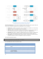
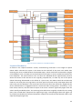
which the executable is running is largely irrelevant. On the MP7, this has been achieved using the
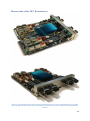
layers of abstraction shown in Figure 1; a concrete example of the distinct regions is shown in Figure
2.
Figure 1 : The model of abstraction used in defining the MP7 firmware
Figure 2 : Firmware implementation in an MP7-R1 690 used in a CERN integration test. The firmware clearly
demonstrates the same segregation shown in the abstract model, with the “MGTs and DAQ buffers” regions
corresponding to the blue and green “layers” in Figure 1, and the “DAQ” and “Communication” regions corresponding to
the grey control block. The central, unlabelled part of the firmware is the firmware dedicated to the user’s algorithms.
10
Core firmware
Link control
The top level entity mp7_mgt provides access to the serial links in groups of 4 links called “quads”.
The number of quads is set by the generic NQUAD. The other generics, CLOCK_RATIO and
LHC_BUNCH_COUNT, refer to the ratio between the LHC clock (40MHz) and the data rate in/out of
the transceiver (e.g. the CLOCK_RATIO = 6 if the data is clocked at 240MHz). The
LHC_BUNCH_COUNT is simply the number of bunch crossing per orbit (3564 for LHC, but for
debugging it can be useful to reduce this).
The core has 4 ipbus interfaces for controlling: channel functionality, channel alignment, and the
internal transceiver characteristics at both the channel level and the characteristics common to all
channels via the Dynamic Reconfiguration Ports (DRP). The signal qsel selects which quad is selected
for ipbus communication ant any given time.
The utility clock sysclk should always be present. It is used to drive startup state machines in the
transceiver. At present this is sourced from the 125MHz free running clock clk_fr.
The reset signals rst_p and rst_cntrl are all in the processing clock clk_p domain (i.e. typically
160MHz or 240MHz). The reset signal is provided to each quad with rst_p. The alignment
mechanism that is performed at a global level is controlled by rst_cntrl.
Data to/from the quad (d and q) is presented in the form of an array of links of type ldata that is
made up of the record type lword than contains a 32bit data word and data valid signal. The serial
interface to the transceiver is presented by refclkp/n, Rxp/n and Txp/n.
Link control at a global level (i.e. latency and alignment)
Components quad_wrapper_gth and Rxdata_simple_cdc_ctrl are the significant components within
mp7_mgt. The former simply wraps the main quad code ext_align_gth_spartan with an ipbus
interface. The latter, Rxdata_simple_cdc_ctrl allows control of the cdc – clock domain crossing
buffer that is instantiated for each channel. This buffer bridges from the transceiver Rxuserclk2 clock
domain, whether it be asynchronous or synchronous to the LHC clock, to the processing clock
domain. In the synchronous case the Rxuserclk2 clock may be the processing clock and a dual port
ram would not be needed; however, there would still need to be a FIFO like object to align links and
provide the option of latency control. The buffer (dual port ram) relaxes the operational
characteristics of the transceiver and makes the system more flexible, albeit with a small increase in
latency that can be offset by running the links at a slightly faster asynchronous rate (internal
transceiver logic runs faster).
Originally there was a dedicated buffer control logic for each channel, but because of concern over
logic resource usage it was extracted and placed at a global level (Rxdata_simple_cdc_ctrl). The
advantage of this is that automatically minimising latency across channels becomes simple; however,
it is necessary to have intermediate FFs to meet timing, particularly when sending the align_marker
signal (i.e. the marker in each link that other links should be aligned to) from the buffer to the
central logic because the signal is travelling from the periphery to the centre and thus clock skew is
not negligible.
11
The buffer control is intended to be quite simple. There are just 4 signals; buf_ptr_inc and
buf_ptr_dec which increment or decrement the buffer read pointer (i.e. adjusting latency); buf_rst
which resets the read and write pointers; and buf_master which indicates to the channel if it is the
master link. If the channel is the master then the buffer read pointer is set to 50 rather than 0 upon
buf_rst. This guarantees that the read pointer from all links other than the master link will need to
be incremented, rather than decremented to achieve alignment.
The write pointer is set to 110 (i.e. far end of the buffer to ensure no overlap with read pointer after
reset). Hence, after reset the buffer data is valid (i.e. no read/write pointer clash), but the links are
not aligned and the latency is large.
Upon receipt of the align_marker signal from the master link (i.e. align_master) all links are checked
for alignment. If a link is not aligned the buffer read pointer is incremented. This process repeats
until all the links are aligned.
Next, all read pointers, including the master, are incremented until the pointer read/write clash
occurs (i.e. we have reduced the latency too much so that the read occurs before the write has
completed). This is detected by a jump in the position of the master alignment marker and/or by loss
of alignment. While it is highly likely with 72 channels that loss of alignment will occur in the
read/write pointer overlap area this may not be the case for a few channels and will not work at all if
just the master link is selected. Hence, the only way to detect the read/write pointer overlap area is
to monitor if the master link position moves; this in turn requires that we can predict the next
master link alignment marker; which forces the master alignment signal to be periodic. This is
normally the case for CMS experiments, in which there is generally 1 marker per orbit; however,
care must be taken in more complex arrangements (e.g. Time Multiplexed Trigger).
When the read/write pointer clash has been detected the firmware decrements to read pointers of
all links so that there is some margin between the read/write pointers. This is the align_margin
parameter and some experimentation may be required to see how small this can be made and for
the links to be stable.
Note that at present this firmware simply minimises latency. It may be necessary to augment the
functionality of the block so that the latency (i.e. read pointer location) is set in relation to TTC and
thus fixed.
Link control at a local level (i.e. protocols, line rates, error checking)
The main link functionality (i.e. error checking, line protocol definition and the Rx buffer) is defined
in the entity ext_align_gth_spartan, which is wrapped by the entity quad_wrapper_gth so that an
ipbus interface can be added and the object used at the global level.
The process of transmitting data out of the transceiver consists of the following steps: a CRC is
appended at the end of the data stream, as defined by the end of the data valid signal; the data is
bridged from the processing clock domain (i.e. typically 160MHz or 240MHz) to that necessary for
the line rate (i.e. 250MHz for 10Gb/s) with padding words inserted if necessary; the data words are
replaced with 8b/10b k-codes where data valid is de-asserted so that the 8b/10b byte alignment can
be performed (comma = 0x505050BC with “charisk” set to 0b0001) or where padding words have
been inserted (padding word = 0xF7F7F7F7 with “charisk” set to 0b1111);
12
The receive data path consists of is first passing the data through the Rx buffer entity
Rxdata_simple_cdc_buf, which allows the data to be delayed for link alignment and latency control.
It also performs the clock bridging from the link clock domain, which is defined by the line rate to the
processing clock domain by stripping out any padding words; lastly the CRC is then checked and
stripped from the packet. The align marker (i.e. the event within the data stream that is used for
alignment) is also defined here, although it could be overwritten at a higher level if a user wanted to
use something other than the start of the packet.
Coming in the next version of this document. In the meantime, please
contact [email protected] or [email protected]
User firmware
As stated previously, the firmware model used is one where the user’s algorithms firmware is fully
abstracted from the details of the hardware implementation. The entity declaration for the user’s
code is shown here:
use work.mp7_data_types.all;
use work.ipbus.all;
entity algo is
generic(
NCHAN: positive
);
port(
ipbus_clk: in std_logic;
ipbus_in:
in ipb_wbus;
ipbus_out: out ipb_rbus;
data_clk:
in std_logic;
data_in:
in ldata(NCHAN - 1 downto 0);
data_out:
out ldata(NCHAN - 1 downto 0)
);
end algo;
Where:
NCHAN is the number of optical data channels available. For MP7 cards built with an
XC7VX485T FPGA, this is always 48. For MP7 cards built with an XC7VX690T FPGA, this is
always 72.
13
ipbus_clk, ipbus_in and ipbus_out are the IPbus control bus for configuring the algorithms.
The use of these signals is described elsewhere.
Reference for use of IPbus is coming in the next version of this
document. In the meantime, please contact [email protected]
data_in and data_out are the input and output pipes which are externally connected to the
optical links, with data being clocked through both pipes on the rising edge of signal
data_clk.
Type ldata is an unconstrained array of type lword, where lword is a record with entries:
o data – a 32-bit std_logic_vector
o valid – a std_logic flag indicating whether or not the accompanying data is valid.
In theory the interface to the QDR ram could also be exposed, although the use case for this has not
yet been demonstrated. There may also be a use case for a reset line.
Dave – is there a use case for a reset line?
Coming in the next version of this document. In the meantime, please
contact [email protected]
Building Firmwares
Because of the complexities involved in collaboratively building firmwares, a TCL-based build system
is used for building firmwares which are based on components in the CACTUS library.
To create a new firmware for the MP7, perform the following operations:
1. If you do not already have a copy, check out the CACTUS trunk. Either:
Full Checkout:
svn co https://svn.cern.ch/reps/cactus/trunk \
/opt/cactus
Minimal Checkout (just firmware components):
svn co https://svn.cern.ch/reps/cactus/trunk/boards \
https://svn.cern.ch/reps/cactus/trunk/components \
/opt/cactus/trunk
Where the /opt/cactus may be set to whichever location you wish to install CACTUS in.
2. Run the following BASH commands:
14
export MP7_VERSION="mp7_485" # or "mp7_690es"
export CACTUS_TRUNK="/opt/cactus/trunk"
ln -sf ${CACTUS_TRUNK}/boards/mp7/base_fw/${MP7_VERSION}/ .
ln -sf ${CACTUS_TRUNK}/components/ipbus/ .
ln -sf ${CACTUS_TRUNK}/components/mp7_ctrl/ .
ln -sf ${CACTUS_TRUNK}/components/mp7_counters/ .
ln -sf ${CACTUS_TRUNK}/components/mp7_xpoint/ .
ln -sf ${CACTUS_TRUNK}/components/opencores_i2c/ .
ln -sf ${CACTUS_TRUNK}/components/mp7_ttc/ .
ln -sf ${CACTUS_TRUNK}/components/mp7_mgt/ .
ln -sf ${CACTUS_TRUNK}/components/mp7_buffers/ .
cp -rf ${CACTUS_TRUNK}/components/mp7_algo/ main
ln -sf main mp7_algo
export REPOS_FW_DIR=`pwd`
export REPOS_BUILD_DIR=`pwd`/${MP7_VERSION}/ise14
mkdir work
cd work
source $REPOS_FW_DIR/ipbus/firmware/example_designs/scripts/setup.sh
cd ..
Making sure to set the CACTUS_TRUNK and MP7_VERSION environment variables
appropriately.
3. Change into the work directory and open the generated xise file using ISE.
4. Add your algorithm code to the file main/firmware/hdl/null_algo.vhd
Coming in the next version of this document. In the meantime, please
contact [email protected]
15
Programming the MP7
The board has the multiple means of programming:
JTAG
Remote programming over IPbus
Direct programming of the SD card
The JTAG chain is described in the section “JTAG chain” on page 37 in the chapter “Hardware – full
specification”. If you cannot see the XC7VX690T in your JTAG chain, please see the section “Trying to
reprogram the FPGA gives me a wrong or unknown device in IMPACT!” on page 50 in the section
“Hardware trouble-shooting”.
Loading new firmwares over GbE has recently been achieved and is currently in the final stages of
testing. When this is complete, a new version of this document will be released. The MMC will need
updating before remote uploading will work.
TO DO: Documentation on how to program over GbE.
Directly programming the SD card can be a little awkward:
1. Using IMPACT, create a PROM file, using the parameters:
Generic Parallel PROM
Auto Select PROM
File Format: BIN (Swap Bits ON)
2. From SVN, check out:
svn co https://svn.cern.ch/reps/cactus/trunk/components/imperial_mmc
3. Change into the “imperial_mmc/tools/imgtool” directory and run “make” to create the
“imgtool” executable
16
4. If using an external card-reader, plug it into your linux PC WITHOUT THE SD CARD INSERTED.
5. Insert the SD card.
6. Run “sudo /sbin/fdisk -l”. There should be an entry that says “Disk XXX doesn't contain a
valid partition table”. Note the name of this disk.
7. Run “sudo chmod 777 XXX”
8. The “imgtool” executable has several options. The usage options can be seen by running
“./imgtool ?”:
Command
format <label>
list
add <name> <file>
get <name> <file>
del <name>
check <name>
swap
9. Usage of “imgtool” is, then,
Description
Formats an image
List files in an image
Adds a file to an image
Gets a file from an image
Deletes a file from an image
Verifies the checksum of a file
Byte swap an image
./imgtool XXX Command [parameters]
10. To prepare an SD card do:
./imgtool XXX format Firmware
./imgtool XXX add YYY.bin ZZZ.bin
./imgtool XXX swap
Where XXX is the name of the SD card as reported by “fdisk” in step 6, YYY.bin is the name
you wish the firmware to have on the SD card and ZZZ.bin is the name of the PROM file
created in step 1. This formats the SD and gives it the volume name “Firmware”.
On old versions of the MMC, only one firmware image is supported and that image must
always be called “ipbus2.bin”; if this file does not exist on the SD card, the FPGA will not be
programmed.
On the latest version of the MMC, the name of the firmware image from which the card is
booted at power-up must always be “GoldenImage.bin”; if this file does not exist on the SD
card, the FPGA will not be programmed at power-up and so Ethernet access will not be
available.
11. To list the contents of an existing SD card:
./imgtool XXX swap
./imgtool XXX list
./imgtool XXX swap
17
The swap command is (currently) required as the file allocation table is read NATIVE endian. The
Atmel UC3A3256, is big-endian, whereas most PCs are little-endian and so the endianness must be
swapped before it may be read by a PC and then swapped back before it is given to the
microcontroller. It is proposed that this will change in future and the endianness handled
automatically in “imgtool”.
The checksum functionality currently has a bug in the implementation and should not be used.
To boot from the SD card, dip-switch 5 on the MP7-R0 and dip-switch 4 on the MP7-R1 or MP7-XE
must be down.
18
Software Overview
Coming in the next version of this document. In the meantime, please
contact [email protected]
Core software: Standard scripts provided for quick configuration
For instructions on how to get the standard MP7 scripts, please see section “Getting started:
Software Installation” on page 7 in the chapter “Getting started”.
Setting clock and TTC inputs
The MP7 can either generate the 40 MHz clock internally, use an external clock generator or the TTC
clock from the AMC13. TTC signals and in particularly BC0s are used in synchronization and data
capture procedures. The MP7 can generate BC0 signals internally, in case no external generator is
available. The mp7-test-reset.py script shows how to reset an MP7 board and configure 40 MHz
clock and reference clock. Two clock configurations are supported by mp7-test-reset.py:
External 40 Mhz clock and external TTC signals
mp7-test-reset.py --clk40=external
TTC inputs are enabled as well.
Internal 40 MHz clock and BC0
mp7-test-reset.py --clk40=internal
External TTC inputs are disabled whilst the internal BC0 generator is active.
In case the MP7 responds on a different ip address, the connection uri can be set using the –uri flag.
The configuration is completed if clock 40 and BC0 are successfully locked.
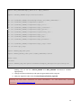
---------------------------------------MP7 Reset and Clock configuration script
---------------------------------------MP7_TEST access successful
WARNING
| Resetting board MP7_LAB_TEST
INFO
| Reset done
INFO
| Configuring clock 40 external
INFO
| Configuring Xpoint
INFO
| Configuring SI5326
INFO
|
Using
etc/config/mp7/si5326/
MP7_SI5326_20130606_40.1MHz_CKIN1_to_160.4MHz_CKOUT1_NoIncDec_Regs.Txt
INFO
| Measuring clk40 frequency. Give me a second...
19
INFO
|
Clock 40 frequency: 39.999720 Mhz
INFO
| Configuring ttc
INFO
| Resetting algos
INFO
|
Measured f40 : 39.999720 Mhz
INFO
|
BC0 reg
INFO
|
BC0 Internal : 0
INFO
|
BC0 Lock
: 1
INFO
|
BC0 Error
: 0
INFO
|
Status: 00000001 BC0 stat: dec14, Bunch 569 Evt: 1, Orb 23
: dec1
Link configuration and alignment in loopback mode
The MP7 links have 2 operation modes: standard and loopback. In loopback mode, for each link the
output data stream is rerouted to the input after the link serialization stage. The input data must be
aligned when entering the algorithm block. The MP7 core firmware provides a mechanism to
automatically align the incoming data from all channels.
An example on how to configure and align the MP7 links is in the mp7-test-mgtconfig.py script.
mp7-test-configlinks.py MP7_TEST --loopback
The command line syntax slightly differs from mp7-test-reset.py. The script first argument is the
name of the board to connect to as specified in the connection file, tests/etc/uhal/connectionstest.xml by default.
The script includes two stages: link configuration and input link alignment. Both need to be
completed for the configuration to be considered successful. The --loopback option enables the
loopback mode. When in loopback mode a self-generated pattern from the Tx buffers is used to
align the Rx inputs. After alignment completion, all the channels are checked for CRC errors and
alignment errors. If required, the board can be reset before configuring the links, using --reset
option.
------------------------------------------MP7 Link configuration and alignment script
------------------------------------------MP7_TEST access successful
INFO
| MP7_TEST built
INFO
| Rx buffer disabled
INFO
| Tx buffer configured for pattern generation
INFO
| Configuring Quads [0]
INFO
| Done
INFO
| Clearing counters
20
INFO
| Alignment
INFO
| --Status: c0000018
INFO
| Checking Quads for errors
INFO
| Clock 40 is locked
INFO
|
+ Alignment: Ok
INFO
|
+ CRCs: []
Capturing input and output data stream
A basic introduction of the MP7 buffer system is provided here. For a more comprehensive
description please refer to the “Core firmware” section on page “11”.
Figure 3: Link buffers and generators
For each link, the incoming data can be routed to a buffer where to be capture. Alternatively the
same buffer can operate in playback mode: the pattern loaded via IPbus is played back every orbit
into the algorithm block. Eventually, a generator is included as well, that produces a hardcoded
pattern every orbit. The same structure is replicated on the output line, after the algorithm block as
shown in Figure 3.
Each buffer is 1024 entries deep. Each entry has 33bits. The first 32 bits are the data payload; bit 33
is the data-valid bit.
The buffers operation mode is configurable via IPbus. When set to capture, the buffers are filled with
data over a user-selected bunch crossing range. When the buffer block is in playback mode, the user
must define a bunch crossing range as well: within the range the data valid bit is used, outside data
valid is forcefully set to low. The data capture is triggered via IPbus. The capture data is accessible via
IPbus as well.
21
a)
b)
c)
d)
Figure 4: Schematic view of the available link buffer configurations.
a) Simple loop b) Link loop c) Algorithm test d) Data capture
mp7-test-datacapture.py is a test script to configure the MP7 link buffer system, capture data and
save it to file. The buffers configurations can be grouped in 4 main categories:
Simple loop: Tx buffers are the data source, connected to Rx buffers via an direct loop
(Figure 4a). Used to test the buffer system functionalities.
Link loop: similar to the previous category, but the loopback connection goes through the
links serialization/deserialization stage (Figure 4b). Requires the --loopback option.
Algorithm test: Useful to validate the algorithm block with user pattern or Monte-Carlo
data. The data is generated by the Rx buffers, and captured by the Tx buffers (Figure 4c).
Data capture: As in standard operation mode, the data is received from an external source.
Tx buffers, Rx buffers or both are configured for capture (see Figure 4c).
The details command line syntax is
mp7-test-datacapture.py MP7_TEST -m <mode>
The -m/--mode option selects the operation mode
Mode
disabled
algoPlay
algoPatt
loopPlayB2B
loopPlayMGT
loopPattB2B
22
Description
No capture. Both Tx and Rx buffers are disabled.
Rx buffer data played back into the algorithm
block.
Hardcoded pattern into the algorithm block
Direct buffer to buffer loop, with data playback
Buffer to buffer loop via the MGT loopback,
with data playback.
Requires --loopback
Direct buffer to buffer loop, with hardcoded
Tx
disabled
capture
Rx
disabled
playback
capture
playback
pattern
pattern
capture
capture
playback
capture
pattern
loopPattMGT Buffer to buffer loop via the MGT loopback,
with hardcoded pattern.
Requires –loopback.
captureRx
Rx buffer capture
captureTx
Tx buffer capture
captureRxTx
Rx and Tx capture
'Rx': receiving buffers, 'Tx': transmitting buffers
pattern
capture
disabled
capture
capture
capture
disabled
capture
Additional options are:
--inject: to specifies what data to upload to the buffers configured for playback.
--path: to select in what folder the captured data is saved.
--reset, --align and --loopback with the same functionality as in mp7-test-configlinks.py.
The capture and playback bunch crossing ranges are temporarily hard-coded to bunch-crossings 0 to
170.
Data format
The mp7 software uses a standard format to export and import data from the board buffers. This
format is used both for data injection and data capture, and automatically converted by the mp7
library into the native buffer format.
An example of data file is shown below (4 channels only)
Board MP7_TEST
Quad/Chan :
Link :
q00c0
q00c1
q00c2
q00c3
00
01
02
03
Frame 0000 : 0v00000000 0v00010000 0v00020000 0v00030000
Frame 0001 : 0v00000001 0v00010001 0v00020001 0v00030001
Frame 0002 : 0v00000002 0v00010002 0v00020002 0v00030002
Frame 0003 : 0v00000003 0v00010003 0v00020003 0v00030003
Frame 0004 : 0v00000004 0v00010004 0v00020004 0v00030004
Frame 0005 : 0v00000005 0v00010005 0v00020005 0v00030005
Frame 0006 : 0v00000006 0v00010006 0v00020006 0v00030006
Frame 0007 : 0v00000007 0v00010007 0v00020007 0v00030007
Frame 0008 : 0v00000008 0v00010008 0v00020008 0v00030008
Frame 0009 : 0v00000009 0v00010009 0v00020009 0v00030009
Frame 0010 : 0v0000000a 0v0001000a 0v0002000a 0v0003000a
Frame 0011 : 0v0000000b 0v0001000b 0v0002000b 0v0003000b
Frame 0012 : 0v0000000c 0v0001000c 0v0002000c 0v0003000c
The first 3 rows are the header. Multiple data blocks can be stored in the same file, if necessary. The
Board field is used to identify the block in the file. The Quad/Chan and Link rows are included to
23
increase readability and are not used. The rows starting with Frame dddd: (dddd is the frame
number in decimal representation), are the payloads. The elements in the row have the format
XvYYYYYYY, where YYYYYYYY a the 32-bit word in hex format and X is the data-valid bit.
Configuring AMC13 to generate clock and L1A/BC0s signals
The AMC13 board has the capability to generate internal clock 40 and feed them to the AMCs in the
uTCA crate. L1As and BC0s can be generated as well connecting the TTS output to the TTC input. See
the AMC13 documentation for further information. A basic script to configure the AMC13 is
included in the MP7 tests package
amc13-setupInternalTTC.py -N <serialNumber>
Checking TTC input
In case debugging the TTC inputs is needed, the MP7 can capture and store up to 2048 L1As and B
commands. For each signal, bunch crossing, orbit and command are recorded as well as the
command type.
The mp7-test-ttchistory.py script allows to capture the TTChistory from command line.
mp7-test-ttccapture.py MP7_TEST
In addition, the --maskBC0 option can be used to avoid storing BC0s in the TTC history,
---------------------------------------MP7 TTC capture script
---------------------------------------MP7_TEST access successful
INFO
| MP7_TEST built
0 | V:1 L1A:0 orb:0x000001 bx:0xd3e cmd:74
1 | V:1 L1A:0 orb:0x000001 bx:0xd3e cmd:75
2 | V:1 L1A:0 orb:0x000001 bx:0xd3e cmd:76
3 | V:1 L1A:0 orb:0x000001 bx:0xd3e cmd:77
4 | V:1 L1A:0 orb:0x000001 bx:0xd3e cmd:78
5 | V:1 L1A:0 orb:0x000001 bx:0xd3e cmd:79
6 | V:1 L1A:0 orb:0x000001 bx:0xd3e cmd:7a
7 | V:1 L1A:0 orb:0x000001 bx:0xd3e cmd:7b
8 | V:1 L1A:0 orb:0x000001 bx:0xd3e cmd:7c
9 | V:1 L1A:0 orb:0x000001 bx:0xd3e cmd:7d
10 | V:1 L1A:0 orb:0x000001 bx:0xd3e cmd:7e
11 | V:1 L1A:0 orb:0x000001 bx:0xd3e cmd:7f
12 | V:1 L1A:0 orb:0x000001 bx:0xd3e cmd:80
24
13 | V:1 L1A:0 orb:0x000001 bx:0xd3e cmd:8
14 | V:1 L1A:0 orb:0x000001 bx:0xd3e cmd:82
15 | V:1 L1A:0 orb:0x000001 bx:0xd3e cmd:83
Legend:
V: data valid
L1A: the command is a L1A
orb: orbit number
bx: bunch crossing
cmd: BGo command
Core software: The C++ components
Coming in the next version of this document. In the meantime, please
contact [email protected]
Description of the core software
o Briefly cover principle of uHAL operation
o Cover derived nodes provided for MP7
Description of the programs provided for standard functions and out-of-the-box testing
User software
Coming in the next version of this document. In the meantime, please
contact [email protected]
Guide for how to write a program which uses and extends the core software
25
MMC, monitoring and IPMI
The Atmel AT32-UC3A-3256 [17] 32-bit microcontroller (MMC) manages the power supplies on the
MP7, provides IPMI functionality and configures the sensor readout. It supports both USB-2 and a
microSDHC card interfaces, such that the MMC can be programmed via USB, and firmware
uploaded to the FPGA from a microSD card. It is responsible for configuring network settings on the
MP7, which allows the FPGA to be programmed via the gigabit ethernet connection on the
backplane. The firmware that provides this functionality is pre-installed onto the MMC before
distribution. The MMC has a single user flash page dedicated to user data storage. This is used to
store the FRU info and persistent user settings such as the IP address or the FPGA boot image file
name. This section provides details on how to utilize the MMC functionality to set up the MP7 for
operation and monitor its sensors.
Firmware upload to FPGA from microSD card
The SD-card is formatted with a file-system known as simple firmware file-system (SFWFS). The
storage medium is divided into “slots” around the size of a firmware image, guaranteeing an image
can be stored without fragmentation. An index table at the front of the disk stores whether a slot is
in use, a file name, file size and checksum, which allows access by name. A full library of SFWFS
operations is included. The image files are stored in the blocks after the header. They do not require
their own header and just start at the appropriate block (slot) and end before the next image. Any
unused space in the slot should be padded with 0xFFFFFFFF if the images are being used to configure
the FPGA.
Sensor monitoring
In the course of debugging the sensors on the MP7, it has come to light that there is a bug in
“ipmitool” which can cause sensors to incorrectly appear as “Disabled”. When using “ipmiutil” or
“NatView”, these sensors are seen to operate correctly.
There are 8 LTC2990 sensors on the MP7 that are monitored using the IPMI out-of-band
management protocol. The raw values from the sensors are converted according to settings in the
sensor data repository (SDR) written to the MMC. The sensor readings can be retrieved using the
ipmitool software [34] or the NatView program [35].
With ipmitool, the sensors can be readout from the command line with:
ipmitool -H [address1] -A none sdr entity [address2]
where the first address is that of the MCH module, and the second address is the board location in
the μTCA crate. The rest of the options shown above are explained in the ipmitool manual. Please
note that use of the ipmitool software requires the OpenIPMI package [36] (included in standard
distributions). The command above returns a list detailing the sensors names and corresponding
measurements. If the sensor reading is outside of the range nominal value ± nominal value, the
command will return status ns (not set) and Disabled for that sensor. This does not necessarily mean
that the sensor is not operating but that the value is not within the correct range to be converted
and sent as a 8-bit signed int over IPMI. Details of all boards in the crate, including the board address
(address2 above) and the status of sensors can be listed using the command:
26
ipmitool -H 192.168.0.41 -A none sensor
To monitor the sensor output in NatView, one must open the program and first connect to the MCH
module by clicking on the “Connect” icon at the top left, and enter the MCH IP address. Once
successfully connected, the program will display all boards running in that crate, and the complete
list of sensor readings is then available. Natview also has the ability to record and log events, as well
as set alarms (depending on what thresholds are set in the SDR).
Setting the IP and Mac addresses
To configure the board addresses, first set the Mac address by running ipmitool with the command:
ipmitool -H [address1] -P "" -B 0 -T 0x82 -b 7 -t [address3] raw [Mac
address]
where address3 is the position of the board in the crate, according to the μTCA specification [37]:
Addr = 0x70 + (S * 2)
e.g. the address of slot AMC08 is 0x80. The Mac address is input using hexadecimal numerals
separated with a space.
The 0x82 address in the command above is the IPMB-0 address of the carrier manager and this
should not be changed.
The IP address should then be set using:
ipmitool -H [address1] -P "" -B 0 -T 0x82 -b 7 -t [address3] raw [IP
address]
where the IP address is again input using hexadecimal numerals separated by a space.
The settings should then be saved by writing to the EEPROM to ensure that the addresses are not
reset to default when the board is power cycled. This is done with the command:
ipmitool -H 192.168.0.41 -P "" -B 0 -T 0x82 -b 7 -t 0x86 raw 0x30 0x01
0xFE 0xEF
The data bytes at the end of this command are a magic word to prevent accidental EEPROM writes.
To display the current network settings of the board, use the command:
ipmitool -H 192.168.0.41 -P "" -B 0 -T 0x82 -b 7 -t 0x86 raw 0x30 0x04
which returns the IP and Mac addresses in the format IP[0].. IP[3]
MAC[0].. MAC[5] FLAGS.
27
Flags is a bitmask. The only bit that is currently used is 0x80. If this is returned, the network
parameters have been modified but not written to the EEPROM.
Power cycling
Coming in the next version of this document. In the meantime, please
contact [email protected]
IPbus to MMC interface
Coming in the next version of this document. In the meantime, please
contact [email protected] or [email protected]
28
Hardware – overview
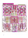
The board layout of the top and bottom faces of the MP7-R0 and MP7-R1 cards can be seen in Figure
5. ...
Coming in the next version of this document. In the meantime, please
contact [email protected] or [email protected]
29
a : Top face
30
b : Bottom face (projected through board)
Figure 5 : Annotated layout of the MP7-R0 and MP7-R1 cards. The MP7-XE layout is similar, except that many of the
clocking components are relocated to the top face of the card.
31
Hardware – full specification
PCB
Whilst the Mini-T5 was built on an FR4 PCB, the MP7-R0 and MP7-R1 are built on a Nelco N4000-13
EP SI, substrate [7] because of the latter’s superior high-frequency characteristics. A 16-layer stackup is used, as shown in Figure 6.
Figure 6 : Layer stack-up for the MP7. Nelco N4000-13 EP SI is used, rather than FR4, because of its superior highfrequency characteristics. Thicknesses measured in thousandths of an inch unless otherwise stated.
To prevent skew across the members of the high-speed differential pairs, the alignment of the
weave of the PCB is to be at an angle of 22 degrees relative to the orientation of the board, so that
neither the horizontal, the vertical nor the diagonal traces are aligned with the PCB weave.
Due to issues with material availability and problems with the hydrophilic properties of NELCO, for
the MP7-XE, … was chosen as the preferred material.
Greg – can you comment please?
In
the
meantime,
[email protected]
32
please
contact
[email protected]
or
FPGA
The MP7 uses a mid-range Xilinx Virtex-7 FPGAs of one of four pin-compatible parts:
•
•
•
•
XC7VX415T (48 GTH links)
XC7VX485T (56 GTX links)
XC7VX550T (80 GTH links)
XC7VX690T (80 GTH links)
With all being available in a 45mm × 45mm, FFG1927 package.
GTX transceivers support selected line-rates up to 12.5 Gb/s in the “-3E” and “-2GE” speed-grades
and up to 10.3125 Gb/s in the “2C”, “-2LE”, and “-2l” speed-grades. GTH transceivers support
selected line-rates up to 13.1 Gb/s in the “-3E” and “-2GE” speed-grades, up to 11.3 Gb/s in the “2C”
and “-2LE” speed-grades and up to 10.3125 Gb/s in the “-2l” speed-grade.
The wide range of pin-compatible parts and speed-grades allows for flexibility in balancing cost and
performance. A comparison of the four pin-compatible parts can be seen in Figure 7.
Figure 7 : Comparison of the Xilinx Virtex-7 series FPGAs which can be used on the MP7 board. Adapted from [8].
The engineering silicon for the Virtex-7 series is the XC7VX485T part with 56 GTX links. The MP7
board has, however, been designed from the outset to accept the XC7VX690T part with 80 GTH links.
The high-speed serial links are divided as:
1 link – Gigabit Ethernet (Backplane)
1 link – Data Acquisition Pathway (Backplane)
1 link – SATA/SAS (Backplane)
1 link – PCI-express/SRIO (Backplane)
4 links – Extended FAT-PIPEs (Backplane)
72 links (XC7VX550T or XC7VX690T) or 48 links (XC7VX485T) – Optical transceivers
33
Optical interface
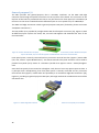
Whilst the Mini-T5 used PPOD optics, there is insufficient front-panel space on a μTCA board to
mount enough PPODs to take full advantage of the Virtex-7’s serial-link capability. Instead, new midboard optics designed for the super-computing industry are used, namely, the Avago MiniPOD [9],
Figure 8.
Figure 8 : Avago MiniPOD optics with unruggedized (left) and ruggedized (right) optical ribbons.
Figure 9 : An example of Avago MiniPODs in use showing how unruggedized optical ribbons can be threaded through
sequential devices.
MiniPODs are pluggable optical devices whose electro-mechanical interface for is a 9×9 MegArray
connector [10], very similar to the 10×10 MegArray connector used by the PPODs on the Mini-T5.
Each MiniPOD device provides 12 serial channels at line-rates of 10.3125Gb/s. Because MiniPODs
are mid-board devices, they may be positioned to minimize the trace-length and maximize signalintegrity. When used with unruggedized fibres, MiniPOD devices can be placed close together and
the ribbons threaded through sequential devices, Figure 9, allowing for a very high data-density.
The MP7 board has 6 MiniPOD transmitter sites and 6 MiniPOD receiver sites giving 72 links in each
direction. For use with an XC7VX485T FPGA, only 4 transmitters and 4 receivers need be fitted,
further reducing cost.
34
Manufacturing constraints on the length of optical ribbon cables constrains the optics to be located
at the back-half of the μTCA card. The optical ribbons enter and leave the MiniPOD devices
approximately 10.5mm above the surface of the PCB; To avoid any risk of the optical ribbons
becoming delaminated in the airflow of a μTCA crate, it was proposed that the ribbons be
mechanically fixed to a structural plane (please see section “Layout & Mechanics”) carrying them to
the front-panel connection at the same height above the PCB as they exit the MiniPOD. It transpires,
however, that the non-peelable optical ribbon [11] used are sufficiently robust so as to eliminate this
risk without the need for additional mechanical support.
The front-panel optical connections are four 48-way MTP connectors [12], of which 36-channels on
each connector are utilized. All channels within each MTP carry data in the same direction. The
interface to external fibres is via MTP-MTP adaptors which are mounted on the front-panel of the
board. The board has been designed to also accept Molex Circular-MT connectors [13], requiring
only a different design of front-panel, should that option be necessary or desirable in future.
Backplane connections
The MP7 uses the same AMC card-edge connector as the Mini-T5, rather than using a component
connector, since space on the board is limited and because such an approach reduces design risk.
As well as Telecoms Clock-A, Fabric Clock-A, geographic addressing, IPMI and JTAG, the AMC cardedge connector features differential connections as shown in Table 1.
Port 0
Port 1
Port 2
Port 3
Port 4
Port 5
Port 6
Port 7
Port 8
Port 9
Port 10
Port 11
Port 12
Port 13
Port 14
Port 15
Port 16
Port 17
Port 18
Port 19
Port 20
Gigabit Ethernet
DAQ
SATA/SAS
TTC/TTS
PCI-express/SRIO
PCI-express/SRIO
PCI-express/SRIO
PCI-express/SRIO
Extended FAT-PIPE
LVDS
LVDS
LVDS
LVDS
LVDS
LVDS
LVDS
Telecoms clock C
Currently Unassigned
Currently Unassigned
Currently Unassigned
Currently Unassigned
Table 1 : Differential connections of the AMC card-edge connector. Ports shaded orange (0, 1, 2 and 4 to 8) are routed to
multi-gigabit transceivers on the FPGA. Ports shaded green (12 to 15) are routed to the general I/O of the FPGA. Ports
shaded red (17 to 20) are currently unassigned. Other AMC card-edge connections not included in this table are
Telecoms Clock-A, Fabric Clock-A, geographic addressing, IPMI and JTAG.
35
General-purpose I/O
The MP7 provides two general-purpose, that is non-MGT, interfaces: via the AMC card-edge
connector and through low-profile connectors on the top-face of the board. The connector on the
top-face of the board is positioned such that it may also be used as front-panel I/O. The Select-I/O
resources on the Virtex-7 FPGA allow each differential pair to run at speeds of up to 1.866 Gbit/s.
The AMC card-edge connection include 7 general-purpose LVDS pairs (for details, please see section
“Backplane connections”).
The low-profile I/O is provided by a single Samtec SS4 ultra-fine-pitch connector [15], Figure 10, with
30 differential pairs to/from the FPGA, 3v3, 2v5 and 1v8 supplies and dedicated I2C lines to the
microcontroller.
Figure 10 : Samtec SS4-ST4 ultra-fine pitch, high-speed connectors. A single such connector provides 30 differential pairs
to/from the FPGA, 3v3, 2v5 and 1v8 supplies and dedicated I2C lines to the microcontroller.
Front-panel space is severely restricted and any connector must be less than (approx.) 37mm wide
(see, also, section “Layout & Mechanics”). The Samtec SS4 ultra-fine-pitch connector can be used to
provide front-panel I/O by means of a miniature (smaller than approx. 37mm × 53mm) daughtercard.
Since the front-panel I/O is mounted on a daughter-card, the user has many options open to them. It
is perhaps worth reemphasizing, that front-panel space is severely restricted and any connector
must be less than (approx.) 37mm wide. One possibility is to use Samtec Edge Rate connectors [16],
Figure 11, providing 16 general-purpose LVDS pairs, although mechanical considerations must still be
checked for this.
Figure 11 : Samtec Edge Rate connector and cable assembly: one proposed solution for front-panel I/O on the MP7
36
MMC-Controller
The MP7 implements MMC functionality using the same 32-bit microcontroller as the Mini-T5,
namely an Atmel AT32-UC3A-3256 [17]. The microcontroller implements IPMI communications and
management and monitoring of the μTCA extraction handle, the temperature & humidity sensors
and the μTCA indicator LEDS. The microcontroller also provides a USB-2 interface to the board, a
serial console and sets the IP-address of the board. The USB connector on the MP7 is a micro-B type
connector, rather than the mini-B type on the Mini-T5, so that it fits on the bottom face of the
board.
The Atmel AT32-UC3A-3256 also supports a microSDHC card interface, and a microSDHC card
connector is also included at the front-panel of the MP7. This is again on the bottom face of the
board.
The software for the MMC-controller has been tested on the Mini-T5 and the board-level
connections of the microcontroller are to be kept as similar as possible, such that the same software
may be used on both boards.
Because of changes in the powering of the Virtex-7 FPGA, it was necessary to reroute the FPGA-tomicrocontroller bus through the CPLD to provide level-translation. This change does not affect the
microcontroller software.
CPLD
As per the Mini-T5, the MP7 uses a Xilinx XC2C256 CoolRunner II CPLD [18]. On the Mini-T5, the
CPLD was primarily used for programmable routing of the JTAG chains. On the MP7, the CPLD is also
be used as a level-translator for various other components, due to the changes in the powering of
the Virtex-7 FPGA.
JTAG chain
The JTAG chain of the MP7 is routed through the CPLD, allowing components to be switched in and
out of the chain and to allow switching between sources, Figure 12. Because the CPLD is itself
programmed via JTAG, the MP7 has two JTAG headers: One for programming the CPLD, which is at
the TOP edge of the board and labelled “CPLD JTAG” and one for programming the components in
the JTAG chain, which is at the BOTTOM edge of the board and is labelled “SWITCHED JTAG”. The
switched JTAG chain is controlled by the DIP-switches, Table 2.
FPGA
Switch
(MP7-R0)
1
Switch
(MP7-R1 and MP7-XE)
8
MMC
2
7
SRAM 1
3
6
SRAM 2
4
5
7
2
Function
UP to exclude from JTAG chain
DOWN to include in JTAG chain
JTAG source
UP for “SWITCHED JTAG” local header
DOWN for AMC connector
Table 2 : Assignment of DIP-switch functionality for selecting the JTAG source and controlling the inclusion/exclusion of
targets from the JTAG chain.
37
Figure 12 : Connections of the JTAG network on the MP7. Two JTAG source, the “Switched JTAG” header and the AMC
connector can be connected to any of four JTAG targets, with the configuration of the chain controlled by the DIP
switches. The CPLD is, itself, programmed by a dedicated JTAG header, labelled “CPLD JTAG”.
To boot from the SD card, dip-switch 5 on the MP7-R0 and dip-switch 4 on the MP7-R1 or MP7-XE
must be down. To boot from the SPI PROM, dip-switch 5 on the MP7-R0 and dip-switch 4 on the
MP7-R1 or MP7-XE must be up.
RAM
The MP7 provides up to 288Mbit of QDR II+ SRAM in the form of 2 × 144Mbit Cypress
CY7C2663KV18-550BZXC (8M×18bit) [19] chips, giving memory access of up to 550MHz DDR
(1100MHz) per chip. The SRAM chosen is pin-compatible with lower-capacity parts and so cost and
performance may be balanced.
The pin compatible parts1 are:
1
18Mbit – CY7C2163KV18 (1M × 18bit)
36Mbit – CY7C2263KV18 (2M × 18 bit)
72Mbit – CY7C25632KV18 (4M x 18 bit)
144Mbit – CY7C2663KV18 (8M × 18 bit)
Although the BGA package of the 18, 36 and 72Mbit parts are physically smaller than the 144Mbit part, the
ball-pitch and electrical connections are identical.
38
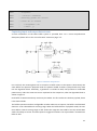
Clocking
The clocking architecture of the MP7-R0 and MP7-R1 cards is based on that of the Mini-T5, with
minor changes to accommodate the difference between the Virtex-5 and the Virtex-7.
The MP7 has LVDS clock inputs from AMC card-edge connections TCLKA, FCLKA and TCLKC. Unlike
the Mini-T5, FCLKA is available for use as a PCIe clock, as well as for distribution of the LHC machine
clock from an AMC13 card located in the redundant slot of a standard dual star μTCA crate. Any of
the AMC clocks may be passed through a Silicon Labs SI5326 [20] jitter attenuator which can also act
in a standalone frequency synthesis mode. The MP7 also accepts a clock input through the front
panel on a pair of SMP connectors[22]. The clocking architecture for the MP7-R0 and MP7-R1 can be
seen in Figure 13.
Figure 13 : Clocking architecture of the MP7-R0 and MP7-R1
On the MP7-R0 and MP7-R1, there are several shortcomings in the clocking architecture which limit
the performance of the board2; The clocking architecture of the MP7-XE has been modified to
rationalize the design, and to provide more flexibility and significantly higher performance.
The shortcomings of the MP7-R0 and MP7-R1 are:
2
I use “limit” here in the most perfectionist way possible. The MP7-R0 and MP7-R1 can run the links at any
speed up to in-excess-of 10Gbps, synchronous or asynchronous. It works.
39
There are two cross-point switches and a fan-out buffer between the SI5326 clock
synthesizer and the MGTs, each component contributing to the additive jitter.
Only one clock is available to each MGT quad
The clock traces are run between power planes, rather than between ground planes
The clocking logic is powered directly from the general-purpose regulators
On the MP7-XE, two independent SI5326 clock-synthesizers are each fanned out through their own
Silicon Labs Si53314 1-to-6 Low Jitter Universal Buffer [21], minimizing additive jitter. Furthermore,
each group of three MGT quads receives two independent clocks allowing mixed clocking modes.
Finally, all clock traces have been routed purely between ground planes and all clocking logic has
been driven by dedicated high-precision LDO regulators, with the option for additional ferrites, to
ensure the cleanest possible clocking environment. The clocking architecture for the MP7-XE can be
seen in Figure 14.
Figure 14 : Clocking architecture of the MP7-XE
40
Power
The MP7 uses a similar power architecture to the Mini-T5, Figure 15.
Figure 15 : Power architecture of the MP7-R0 board. For the MP7-R1, the LTM4628 providing 1v0 is replaced by an
LTM4620, and the LTM4606s providing 1v0 are replaced by LTM4601s.
The main power supplies on the MP7-R0 are Linear Technologies LTM4628 µModule Buck Regulators
[22], each providing two independent supplies at 8A or one supply at 16A. On the MP7-R1 and MP7XE, the 1V core supply is replaced with a Linear Technologies LTM4620 µModule Buck Regulator
[24], which is footprint-compatible with the LTM4628 used on the MP7-R0, but capable of providing
two independent supplies at 13A or one supply at 26A.
On the MP7-R0, power for the MGT banks on the Virtex-7 are provided by Linear Technologies
LTM4606 Ultralow EMI regulators [25], as used on the Mini-T, with dedicated supplies for each of
the two banks. The primary switching supplies are phased to reduce transient loads. On the MP7-R1
and MP7-XE, the 1.0V supplies for the MGT banks were changed to Linear Technologies LTM4601
regulators [26] because of the need for a higher current rating. Naturally, the possibility of power
supply changes introducing noise was a major concern, so several test cards, which could be
41
mounted on a revision-0 card, were produced to test alternative power supply designs. Noise was
measured both electrically and by its effect on the error-rate of the 10Gbps optical links. The noise
performance of all the tested designs was similar, and the design based on the Linear LTM4601
switch-mode regulator was chosen since the LTM4601 is the same size as the LTM4606 and uses
similar external components, making it the simplest and safest replacement.
On the Mini-T5, it is possible to bridge the +3.3V supply to the management-power supply for bench
top operation using a single, +12V supply, by means of a 0.1” header/jumper. This presents the risk
of shorting the power-supplies if the jumper is not removed before the card is inserted into a μTCA
crate. To avoid this possibility on the MP7, the design has been changed to switch between the two
supplies, rather than bridging the two, by using a double throw switch. For convenience, the enable
signal for the switching supplies has been routed from either +12V or the microcontroller by the
same switch.
The CPLD I/O power and the FPGA transceiver-aux power has been supplied by Micrel MIC5319
regulators [27], chosen for their low noise and ultra-small footprint. Specialist regulators are used
for the QDR-termination voltage on the SRAM [28].
To improve the performance of the clocking on the MP7-XE, the clocking components on that board
are also supplied by dedicated Micrel MIC5319 regulators, again chosen for their low noise and
ultra-small footprint The power architecture of the MP7-XE can be seen in Figure 16.
Flash PROM
The MP7 is to use a Micron N25Q256A13ESF40G, 256Mb SPI NOR Flash[29] which is pin compatible
with parts up to 1Gb. Investigations are also on-going into the feasibility of using the microSDHC
card (see, also, section “MMC-Controller”) to store firmware images and to use the MMC-controller
as a boot-loader for the FPGA. Even if this method works satisfactorily, a Flash PROM is still included
in the design.
On-board Monitoring
Systems monitoring is particularly important on the MP7 because of the board’s extreme
performance and the complexity of, and tight requirements placed on, the power supply network.
Linear Technologies LTC2990 Quad I2C Voltage, Current and Temperature Monitors [30] are used to
monitor:
the temperature, output-voltage and current-draw on each of the LTM4628 regulators
the temperature, output-voltage and current-draw on each pair of the LTM4606 regulators
the temperature and supply voltages at the centre of each group of optics
the SRAM termination voltages
It has been suggested that the primary cause of the failure of optical components in the ATLAS
experiment may be the humidity of the operating environment [31] and that the same may apply to
optical failures seen by CMS. Given the high density of optics on the MP7, a SHT21 humidity and
temperature sensor by Sensirion [32] is used to monitor atmospheric humidity.
42
Figure 16 : Power architecture of the MP7-XE board.
Layout & Mechanics
As stated in the “Optical interface” section, manufacturing constraints on the length of optical
ribbon cables constrains the optics to be located at the back-half of the μTCA card. Rather than
mounting the Virtex-7 FPGA between the MiniPOD optics, which would have minimized the lengths
of the 10Gbit/s traces, the FPGA is mounted forward of the optics to ensure unobstructed airflow for
heat dissipation. The optical ribbons enter and leave the MiniPOD devices approximately 10.5mm
above the surface of the PCB and it was originally proposed that, to avoid any risk of the optical
ribbons becoming delaminated in the airflow of a μTCA crate, the ribbons would be mechanically
fixed to a structural plane carrying them to the front-panel connection at the same height above the
PCB as they exit the MiniPOD. It has since been found that the fibres are sufficiently rugged that the
threat of delamination is negligible and that a mechanical fibre routing plane is unnecessary. It has
been found, however, that the thermal output of the Virtex-7 FPGA is significantly higher than the
values initially provided by Xilinx. The mounting holes which were originally included for the routing
plane, have instead been repurposed for supporting a large, custom-designed heat-sink (Figure 21)
to provide considerable extra thermal dissipation compared to the off-the-shelf heatsink used on the
original prototype (Figure 20).
43
The front-panel layout can be seen in Figure 17.
Figure 17 : Front-panel layout of the MP7. Yellow regions indicate μTCA infrastructure zones; red regions contains LEDs,
etc., the purple region contains the micro-USB connector and microSDHC card connector whilst the orange region
indicates the approx. 37mm wide zone available for general-purpose I/O connections. Screw-mount MTP adapters are
required to take up any slack in the ribbon cables manufacturing tolerances. Board layout as of 08/02/2012.
The front-panels for the MP7 are based on front-panel and extraction handle kits by Schroff, part
number 20849-132 [33]. The panels provided with standard MP7 cards will be laser etched with the
decal shown in Figure 18.
Figure 18 : The front-panel design provided with a standard MP7 card.
A prototype front panel is shown in Figure 19.
Figure 19 : Prototype laser-etched front panel
44
Photographs of the MP7-R0 prototype
Figure 20 : Two photographs of the first prototype Imperial MP7 processor card. The optical ribbons used are samples
with an additional prizm connector that is not required in the final design. The Virtex-7 FPGA is located under the blue
heat-sink.
45
Photographs of the MP7 R1
Figure 21 : Two photographs of the Imperial MP7-R1 processor card. The Virtex-7 FPGA is located under the customdesigned black heat-sink.
46
Parts Summary
Part
PCB material
(MP7-R0 & MP7-R1)
PCB material
(MP7-XE)
FPGA
Optics – Transmitter
Optics – Receiver
General-purpose I/O – Topsurface/front-panel
MMC-Controller
CPLD
QDR SRAM
Clocking – Frequency
Synthesiser /Jitter Attenuator
Clocking – 4:4Cross-point
switch
Clocking – 1:4 Fanout Buffers
(MP7-R0 & MP7-R1)
Clocking – 1:6 Fanout Buffers
(MP7-XE)
Front-panel clock inputs
Power – General 3.3V / 2.5V
Power – General 1.8V / 1.5V
Power - General 1.0V (MP7-R0)
Power - General 1.0V (MP7-R1
& MP7-XE)
Power - Transceiver 1.2V
3
Component
Nelco N4000-13 EP SI
Datasheet
http://www.parkelectro.com/parkelectro/im
ages/n4000-13ep.pdf
Xilinx Virtex-7
XC7VX415T, XC7VX485T,
XC7VX550T, XC7VX690T
Avago Technologies MiniPOD
AFBR-81uVxyZ
Avago Technologies MiniPOD
AFBR-82uVxyZ
Samtec SS4 - .4mm (.0157”)
Super Low Profile Socket Strip
SS4-50 - .4mm (.0157”)
Atmel
AT32-UC3A-3256
Xilinx CoolRunner II
XC2C256-6FT256C
Cypress
CY7C2163KV18-550BZXI,
CY7C2263KV18-550BZXI,
CY7C25632KV18-550BZXI,
CY7C2663KV18-550BZXC
Silicon Labs
SI5326
http://www.xilinx.com/support/documentat
ion/data_sheets/ds180_7Series_Overview.p
df
http://www.avagotech.com/pages/minipod_
micropod
http://www.avagotech.com/pages/minipod_
micropod
http://www.samtec.com/documents/webfil
es/cpdf/SS4-XX-X.XX-X-D-X-XX-TR-MKT.pdf
Micrel
SY89540U
Micrel
SY89833AL
Silicon Labs
SI53314
Samtec
SMP-EM - 50 Ohm SMP RF
Plug, Edge Mount
Linear Technology
LTM4628
Linear Technology
LTM4628
Linear Technology
LTM4628
Linear Technology
LTM4620
Linear Technology
LTM4606
http://www.atmel.com/dyn/resources/prod
_documents/doc32072.pdf
http://www.xilinx.com/support/documentat
ion/data_sheets/ds094.pdf
http://www.cypress.com/?docID=32757,
http://www.cypress.com/?docID=31966,
http://www.cypress.com/?docID=27917,
http://www.cypress.com/?docID=33228
http://www.silabs.com/pages/DownloadDoc
.aspx?FILEURL=Support
Documents/TechnicalDocs/Si5326.pdf&src=
DocumentationWebPart3
http://www.micrel.com/_PDF/HBW/sy8954
0u.pdf
http://www.micrel.com/_PDF/HBW/sy8983
3al.pdf
http://www.silabs.com/Support%20Docume
nts/TechnicalDocs/Si53314.pdf
http://www.samtec.com/documents/webfil
es/cpdf/SMP-PX-P-XX-ST-EM3-MKT.pdf
http://cds.linear.com/docs/Datasheet/4628f
b.pdf
http://cds.linear.com/docs/Datasheet/4628f
b.pdf
http://cds.linear.com/docs/Datasheet/4628f
b.pdf
http://cds.linear.com/docs/Datasheet/4620f
a.pdf
http://cds.linear.com/docs/Datasheet/4606f
b.pdf
You may need to manually copy this link into your internet browser
47
Power - Transceiver 1.0V (MP7R0)
Power - Transceiver 1.0V (MP7R1 & MP7-XE)
Power – Transciever aux 1.8V
Power - CPLD 2.5V
Power - CPLD 1.8V
Power - SRAM 0.9V
Flash PROM
Linear Technology
LTM4606
Linear Technology
LTM4601
Micrel
MIC5319
Micrel
MIC5319
Micrel
MIC5319
Richtec
RT9040
Micron Serial NOR Flash
Memory, 3V, Multiple I/O, 4KB
Sector Erase
N25Q256A13ESF40G
Monitoring - Temperature,
Current & Voltage
Monitoring - Humidity
Linear Technology
LTC2990
Sensirion
SHT21
Front-panel
Schroff
20849-132
http://cds.linear.com/docs/Datasheet/4606f
b.pdf
http://cds.linear.com/docs/en/datasheet/46
01fc.pdf
http://www.micrel.com/_PDF/MIC5319.pdf
http://www.micrel.com/_PDF/MIC5319.pdf
http://www.micrel.com/_PDF/MIC5319.pdf
http://tw.richtek.com/download_ds.jsp?s=5
23
http://www.micron.com/parts/norflash/serial-norflash/~/media/Documents/Products/Data%2
0Sheet/NOR%20Flash/Serial%20NOR/N25Q/
5989n25q_256mb_3v_65nm.ashx
http://cds.linear.com/docs/Datasheet/2990f
c.pdf
http://www.sensirion.com/en/pdf/product_i
nformation/Datasheet-humidity-sensorSHT21.pdf
Table 3 : A summary of the component parts for the MP7 board and links to their datasheets. Where there is a choice of
part numbers, the target part is underlined.
48
Hardware trouble-shooting
I was reprogramming the MMC in the Crate and now the MMC is powered
but the rest of the board is not and without the CPLD I cannot JTAG the
MMC!
This is an unfortunate by-product of using the CPLD to route the JTAG chain and of the fact that the
CPLD draws too much current to be safely run on the management power.
The double-pole, double-throw switch mechanism on the power-supply means that the card has two
modes: Desktop mode and Crate mode:
In Crate mode, the MMC enables the bulk supplies and is, itself, enabled by the enable signal from
the AMC connector. If the MMC is bricked by uploading a “bad” program, then it can disable the
power-supplies, breaking the JTAG chain and thus preventing reprogramming of the MMC!
In Desktop mode, the bulk supplies are enabled automatically, since the MMC must be powered
from the bulk 3v3 supply.
The only solution to restore a bricked MMC is to put the card in Desktop mode and reprogram it
with a good image.
Trying to reprogram the MMC gives me errors in AVR32STUDIO!
Does your error look like this?
Your JTAG chain is broken! Three possible causes:
Are the dip-switches correctly? On the MP7-R0, switch 2 should be down and switches 1, 3,
4 and 7 should be up. On the MP7-R1 and MP7-XE, switch 7 should be down and switches 8,
6, 5 and 2 should be up.
You are connected to the wrong JTAG header. Make sure that you are connected to the
“SWITCHED JTAG” header at the bottom edge of the card, not the “CPLD JTAG” header at
the top edge of the card.
Your dongle for adapting the ATMEL-style JTAG header to the Xilinx-style JTAG socket is
broken/faulty.
49
Trying to reprogram the FPGA gives me a wrong or unknown device in
IMPACT!
Does your error look like this?
Your dip-switches are most likely set incorrectly and you are connected to the MMC, not the FPGA.
On the MP7-R0, switch 1 should be down and switches 2, 3, 4 and 7 should be up. On the MP7-R1
and MP7-XE, switch 8 should be down and switches 7, 6, 5 and 2 should be up.
Does your error look like this?
This is the CPLD: you are connected to the wrong JTAG header. Make sure that you are connected to
the “SWITCHED JTAG” header at the bottom edge of the card, not the “CPLD JTAG” header at the
top edge of the card.
My board is booting from the PROM rather than the SD card!
To boot from the SD card, dip-switch 5 on the MP7-R0 and dip-switch 4 on the MP7-R1 or MP7-XE
must be down.
50
References
1
G. Iles and A. Rose, CMS IN2011_008, “A Time-Multiplexed Calorimeter Trigger for CMS” 22
March 2011.
http://cms.cern.ch/iCMS/jsp/openfile.jsp?type=IN&year=2011&files=IN2011_008.pdf.
2
Xilinx Inc., UG190, “Virtex-5 FPGA User Guide” 17 May 2010.
http://www.xilinx.com/support/documentation/user_guides/ug190.pdf.
3
Avago Technologies, “QSFP Pluggable, Parallel Fiber-Optics Module” 18 September 2009.
http://www.avagotech.com/docs/AV02-1839EN.
4
Reflex Photonics Inc., “InterBOARD 40 Gbps SNAP 12 Parallel Fiber Optic Transmitter and
Receiver Board Edge Modules” December 2010. http://reflexphotonics.com/PDFs/SN-970004-00_Rev_3-6_InterBoard_Board-Edge_Data_Sheet.pdf.
5
Avago Technologies, “AFBR-775BxxxZ / AFBR-785BxxxZ Twelve-Channel Transmitter and
Receiver Pluggable, Parallel-Fiber-Optics Modules” 07 August 2009.
http://www.avagotech.com/docs/AV02-2179EN.
6
Xilinx Inc., DS180, “7 Series FPGAs Overview” 13 September 2011.
http://www.xilinx.com/support/documentation/data_sheets/ds180_7Series_Overview.pdf.
7
Park Advanced Circuitry Materials Corp., “Nelco N4000-13 EP SI” Rev 4-11, 2011.
http://www.parkelectro.com/parkelectro/images/n4000-13ep.pdf.
8
Xilinx Inc., “Virtex7 Product Table” http://www.xilinx.com/publications/prod_mktg/Virtex7Product-Table.pdf.
9
Avago Technologies, MiniPOD Twelve-Channel Transmitter, Twelve-Channel Receiver High
Density, Pluggable, Parallel-Fiber-Optics Modules Product Brief, AV02-2842EN, 2011.
10 FCI connect, “MEG-ARRAY CONNECTOR SYSTEM”
http://portal.fciconnect.com/Comergent//fci/documentation/950554-007_meg-array.pdf.
11 Corning Cable Systems LLC , EVO-996-EN , “Non-Peelable Fiber Optic Ribbon, 12 Fibers”
November 2009.
12 US Conec Ltd., “MTP brand connectors” 2011.
http://www.usconec.com/pages/products/connect_adapter/connector/mtpconnector_rev4
.pdf.
13 Molex Inc., “Circular MT Optical Cable Assemblies” 2010.
http://www.molex.com/elqNow/elqRedir.htm?ref=http://rhu004.smapromail.com/SQLImages/kelmscott/Molex/PDF_Images/987650-3051.PDF.
51
14 Larsen, R.S., “PICMG xTCA standards extensions for Physics: New developments and future
plans,” Real Time Conference (RT), 17th IEEE-NPSS , vol., no., pp.1-7, 24-28 May 2010
http://ieeexplore.ieee.org/stamp/stamp.jsp?tp=&arnumber=5750327&isnumber=5750311
15 Samtec Inc., “SS4 - .4mm (.0157”) Super Low Profile Socket Strip” 19 April 2007.
http://www.samtec.com/documents/webfiles/cpdf/SS4-XX-X.XX-X-D-X-XX-TR-MKT.pdf.
16 Samtec Inc., “ERF8-RA - .8mm (.0315”) Edge Rate Socket Strip, Right Angle” 10 August 2010.
http://www.samtec.com/documents/webfiles/cpdf/ERF8-XXX-XX-X-D-RA-XXX-TR-MKT.pdf.
17 Atmel Corp., “AT32UC3A3/A4 Series,” November 2011.
http://www.atmel.com/dyn/resources/prod_documents/doc32072.pdf.
18 Xilinx Inc., DS094, “XC2C256 CoolRunner-II CPLD” 11 September 2008.
http://www.xilinx.com/support/documentation/data_sheets/ds094.pdf.
19 Cypress Semiconductor Corp., “144-Mbit QDR II+ SRAM 4-Word Burst Architecture (2.5 Cycle
Read Latency) with ODT” 6 December 2011. http://www.cypress.com/?docID=33228
20 Silicon Labs Inc. “Si5326 Any Frequency Precision Clock Multiplier/Jitter Attenuator”
September 2010. http://www.silabs.com/pages/DownloadDoc.aspx?FILEURL=Support
Documents/TechnicalDocs/Si5326.pdf&src=DocumentationWebPart4
21 Silicon Labs Inc. “Si53314 1:6 Low Jitter Universal Buffer/Level Translator With 2:1 Input Mux
And Individual OE (<1.25 GHz)” October 2012,
http://www.silabs.com/Support%20Documents/TechnicalDocs/Si53314.pdf
22 Samtec Inc., “SMP-EM - 50 Ohm SMP RF Plug, Edge Mount” 29 October 2010.
http://www.samtec.com/documents/webfiles/cpdf/SMP-PX-P-XX-ST-EM3-MKT.pdf
23 Linear Technology Corp., “LTM4628 Dual 8A or Single 16A DC/DC µModule Regulator” July
2011. http://cds.linear.com/docs/Datasheet/4628fb.pdf
24 Linear Technology Corp., “LTM4620 Dual 13A or Single 26A DC/DC µModule Regulator”
October 2013. http://cds.linear.com/docs/Datasheet/4620fa.pdf
25 Linear Technology Corp., “LTM4606 Ultralow EMI 28VIN, 6A DC/DC µModule Regulator”
March 2011. http://cds.linear.com/docs/Datasheet/4606fb.pdf
26 Linear Technology Corp., “LTM4601/LTM4601-1 12A μModule Regulators with PLL, Output
Tracking and Margining ” March 2012, http://cds.linear.com/docs/en/datasheet/4601fc.pdf
27 Micrel Inc., “MIC5319 500mA μCap Ultra-Low Dropout High PSRR LDO Regulator” May 2010.
http://www.micrel.com/_PDF/MIC5319.pdf
4
You may need to manually copy this link into your internet browser
52
28 Richtek Technology Corp., “RT9040 DDR Termination Regulator” July 2011.
http://tw.richtek.com/download_ds.jsp?s=523
29 Micron Technology, Inc., “Micron Serial NOR Flash Memory, 3V, Multiple I/O, 4KB Sector
Erase” January 2012. http://www.micron.com/parts/nor-flash/serial-norflash/~/media/Documents/Products/Data%20Sheet/NOR%20Flash/Serial%20NOR/N25Q/59
89n25q_256mb_3v_65nm.ashx
30 Linear Technology Corp., “LTC2990 Quad I2C Voltage, Current and Temperature Monitor”
December 2011. http://cds.linear.com/docs/Datasheet/2990fc.pdf
31 Weidberg, T., “Electrical Tapes & Optical Links” Quality Workshop 2011, CERN, 4 November
2011.
https://indico.cern.ch/getFile.py/access?contribId=10&sessionId=9&resId=1&materialId=slid
es&confId=148944
32 Sensirion AG., “SHT21 Humidity and Temperature Sensor IC” May 2010.
http://www.sensirion.com/en/pdf/product_information/Datasheet-humidity-sensorSHT21.pdf
33 Schroff 20849-132 “AdvancedMC module mechanism, pull-handle mechanism, PIGMG
AMC.0 R2.0RC1.2”
34 J. Audet et. al., “IPMItool: open source command-line interface to IPMI-enabled devices”,
http://sourceforge.net/projects/ipmitool/, October 2013.
35 N.A.T. Europe, “NATview: Visualization tool for any MicroTCA system”,
http://www.nateurope.com/products/NATview.html, December 2013.
36 C. Minyard, “IPMI – A Gentle Introduction with OpenIPMI”,
http://openipmi.sourceforge.net/ , February 2006.
37 PICMG, “μTCA Micro Telecommunications Computing Architecture Short Form
Specification”, September 2006.
53
List of Figures
Figure 1 : The model of abstraction used in defining the MP7 firmware ............................................. 10
Figure 2 : Firmware implementation in an MP7-R1 690 used in a CERN integration test. The firmware
clearly demonstrates the same segregation shown in the abstract model, with the “MGTs and DAQ
buffers” regions corresponding to the blue and green “layers” in Figure 1, and the “DAQ” and
“Communication” regions corresponding to the grey control block. The central, unlabelled part of
the firmware is the firmware dedicated to the user’s algorithms........................................................ 10
Figure 3: Link buffers and generators ................................................................................................... 21
Figure 4: Schematic view of the available link buffer configurations. a) Simple loop b) Link loop c)
Algorithm test d) Data capture ............................................................................................................. 22
Figure 5 : Annotated layout of the MP7-R0 and MP7-R1 cards. The MP7-XE layout is similar, except
that many of the clocking components are relocated to the top face of the card. ............................. 31
Figure 6 : Layer stack-up for the MP7. Nelco N4000-13 EP SI is used, rather than FR4, because of its
superior high-frequency characteristics. Thicknesses measured in thousandths of an inch unless
otherwise stated. .................................................................................................................................. 32
Figure 7 : Comparison of the Xilinx Virtex-7 series FPGAs which can be used on the MP7 board.
Adapted from [8]. ................................................................................................................................. 33
Figure 8 : Avago MiniPOD optics with unruggedized (left) and ruggedized (right) optical ribbons. .... 34
Figure 9 : An example of Avago MiniPODs in use showing how unruggedized optical ribbons can be
threaded through sequential devices. .................................................................................................. 34
Figure 10 : Samtec SS4-ST4 ultra-fine pitch, high-speed connectors. A single such connector provides
30 differential pairs to/from the FPGA, 3v3, 2v5 and 1v8 supplies and dedicated I2C lines to the
microcontroller. .................................................................................................................................... 36
Figure 11 : Samtec Edge Rate connector and cable assembly: one proposed solution for front-panel
I/O on the MP7 ..................................................................................................................................... 36
Figure 12 : Connections of the JTAG network on the MP7. Two JTAG source, the “Switched JTAG”
header and the AMC connector can be connected to any of four JTAG targets, with the configuration
of the chain controlled by the DIP switches. The CPLD is, itself, programmed by a dedicated JTAG
header, labelled “CPLD JTAG”. .............................................................................................................. 38
Figure 13 : Clocking architecture of the MP7-R0 and MP7-R1 ............................................................. 39
Figure 14 : Clocking architecture of the MP7-XE .................................................................................. 40
Figure 15 : Power architecture of the MP7-R0 board. For the MP7-R1, the LTM4628 providing 1v0 is
replaced by an LTM4620, and the LTM4606s providing 1v0 are replaced by LTM4601s. ................... 41
Figure 16 : Power architecture of the MP7-XE board. .......................................................................... 43
Figure 17 : Front-panel layout of the MP7. Yellow regions indicate μTCA infrastructure zones; red
regions contains LEDs, etc., the purple region contains the micro-USB connector and microSDHC card
connector whilst the orange region indicates the approx. 37mm wide zone available for general-
54
purpose I/O connections. Screw-mount MTP adapters are required to take up any slack in the ribbon
cables manufacturing tolerances. Board layout as of 08/02/2012. ..................................................... 44
Figure 18 : The front-panel design provided with a standard MP7 card. ............................................. 44
Figure 19 : Prototype laser-etched front panel .................................................................................... 44
Figure 20 : Two photographs of the first prototype Imperial MP7 processor card. The optical ribbons
used are samples with an additional prizm connector that is not required in the final design. The
Virtex-7 FPGA is located under the blue heat-sink. .............................................................................. 45
Figure 21 : Two photographs of the Imperial MP7-R1 processor card. The Virtex-7 FPGA is located
under the custom-designed black heat-sink......................................................................................... 46
List of Tables
Table 1 : Differential connections of the AMC card-edge connector. Ports shaded orange (0, 1, 2 and
4 to 8) are routed to multi-gigabit transceivers on the FPGA. Ports shaded green (12 to 15) are
routed to the general I/O of the FPGA. Ports shaded red (17 to 20) are currently unassigned. Other
AMC card-edge connections not included in this table are Telecoms Clock-A, Fabric Clock-A,
geographic addressing, IPMI and JTAG. ................................................................................................ 35
Table 2 : Assignment of DIP-switch functionality for selecting the JTAG source and controlling the
inclusion/exclusion of targets from the JTAG chain. ............................................................................ 37
Table 3 : A summary of the component parts for the MP7 board and links to their datasheets. Where
there is a choice of part numbers, the target part is underlined. ........................................................ 48
55
Revision History
Revision
0.1
0.2
56
Release Date
15.01.2014
11.02.2014
Notes
Initial release
Add Alessandro’s getting started guide
Add how to program the FPGA