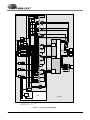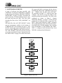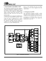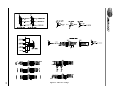
1
CDB49400 Evaluation Board for CS49400 Family DSP Features Description 8 Discrete analog inputs using CS5360 The CDB49400 is an evaluation board for the CS49400 (144 Pin) family of DSPs. It allows customers to develop, download and test custom algorithms on the CS49400. The onboard PLD on the UDSP can route data to any of the audio data inputs and supply clocks in many different combinations to the CS49400. The board interfaces to a PC via a ECP parallel port. Optical and RCA connectors are used to interface with DVD players, powered speakers and other test equipment. Compressed data can be delivered in IEC61937 format via the S/PDIF port. PCM data can be accepted through the digital input connector or from the on-board ADCs. Together these boards supports all the decoding algorithms developed by Cirrus Logic. ADCs 8 Discrete analog outputs using CS4392 DACs Supports 16 Channel decoding capability of the CS49400 1Digital input using the CS8415A S/PDIF receiver 3 Digital outputs using the CS8405 S/PDIF transmitter On board memories for special post processing needs On board debug functionality for DSPC ORDERING INFORMATION CDB49400 Evaluation Board I PARALLEL PORT INTERFACE RS 422 INTERFACE J46 P8 UDSP BOARD REV B MODE SEL RS232 INTERFACE J6 AIO16 P7 CS8405 SPDIF TMTR CS8405 SPDIF TMTR AIO15 CS8405 SPDIF TMTR CS5360 A/D SRAM 512K X 8 AIO14 MICRO AIO13 AUDIO PORT SELECT CS5360 A/D CS5360 A/D AIO10 CS8415 SPDIF RCVR AIO9 TX1 CS5360 A/D FLASH 512K X 8 DSP C DSP AB BOOT BOOT MODE MODE AIO8 AIO7 J11 SW2 CS4392 DAC CS4392 DAC CS4392 DAC AIO6 CS4392 DAC DEBUG PORT SW4 SW3 AIO5 CDB49400 B.0 BOARD SW1 J4 ANALOG INPUTS AIO12 AIO11 SDRAM 512K X 16 CS49400 J26 J29 DIGITAL INPUT HEAD PHONE J5 J3 J2 J1 ANALOG OUTPUTS AIO4 AIO3 AIO2 RX3 DIGITAL OUTPUTS Preliminary Product Information P.O. Box 17847, Austin, Texas 78760 (512) 445 7222 FAX: (512) 445 7581 http://www.cirrus.com RX4 PWR POWER +2.5V RX2 +3.3V RX1 +5 -15 +15 GND AIO1 AUX POWER This document contains information for a new product. Cirrus Logic reserves the right to modify this product without notice. Copyright Cirrus Logic, Inc. 2002 (All Rights Reserved) MAR’ 02 DS536DB1 1 TABLE OF CONTENTS FEATURES .................................................................................................................................... 1 DESCRIPTION ............................................................................................................................... 1 1. QUICK START........................................................................................................................... 4 2. HARDWARE OVERVIEW.......................................................................................................... 5 3. SOFTWARE OVERVIEW .......................................................................................................... 7 4. AUDIO DATA AND CLOCK ROUTING..................................................................................... 8 4.1 SPDIF_ANA_IN_DIG_ANA_OUT.BAT ............................................................................... 8 5. BOOT MODES AND DEBUG PORT ......................................................................................... 9 5.1 Debug Port for DSPC.......................................................................................................... 9 6. EXTERNAL MEMORY INTERFACE ....................................................................................... 10 6.1 SDRAM (U8) ..................................................................................................................... 10 6.2 SRAM (U5)........................................................................................................................ 10 6.3 FLASH (U9) ...................................................................................................................... 10 7. DEFAULT JUMPER SETTINGS ON THE CDB49400 ............................................................ 11 7.1 Host Interface / Boot Modes ............................................................................................. 11 7.2 Host Interface / Boot Mode Jumpers ................................................................................ 11 7.3 Debug Port Interface Jumpers .......................................................................................... 12 7.4 Communication ................................................................................................................ 12 7.5 Serial Audio ...................................................................................................................... 12 7.6 Other Settings ................................................................................................................... 13 8. DEFAULT JUMPER SETTINGS ON UDSP ............................................................................ 14 APPENDIX A: PCM_49400.BAT................................................................................................. 15 APPENDIX B: SPDIF_ANA_IN_DIG_ANA_OUT.BAT ............................................................... 17 APPENDIX C: CDB49400.INI...................................................................................................... 19 APPENDIX D: RESET.BAT......................................................................................................... 20 APPENDIX E: BOARD CONTROL SOFTWARE ........................................................................ 21 APPENDIX F: INSTALLATION OF BOARD CONTROL SOFTWARE....................................... 24 APPENDIX G: CDB49400 SCHEMATICS ........................................................................ 26 APPENDIX H: BILL OF MATERIALS -CDB49400 ..................................................................... 38 APPENDIX I: UDSP SCHEMATICS ................................................................................... 43 APPENDIX J: BILL OF MATERIALS - UDSP............................................................................. 52 2 LIST OF FIGURES Figure 1. Audio Data/Clock Routing................................................................................................ 6 Figure 2. Software Overview........................................................................................................... 7 Figure 3. Sample Data/Clock Routing............................................................................................. 9 Figure 4. Sheet 1 - DSP ................................................................................................................ 26 Figure 5. Sheet 2 - Memory .......................................................................................................... 27 Figure 6. Sheet 3 - ADC - 1........................................................................................................... 28 Figure 7. Sheet 4 - ADC - 2........................................................................................................... 29 Figure 8. Sheet 5 - S/PDIF RCVR................................................................................................. 30 Figure 9. Sheet 6 - DAC - 1........................................................................................................... 31 Figure 10. Sheet 7 - DAC - 2......................................................................................................... 32 Figure 11. Sheet 8 - S/PDIF XCVR............................................................................................... 33 Figure 12. Sheet 9 - Buffers .......................................................................................................... 34 Figure 13. Sheet 10 - Configs. ...................................................................................................... 35 Figure 14. Sheet 11 - UDSP Interface. ......................................................................................... 36 Figure 15. Sheet 12 - Power Supplies .......................................................................................... 37 Figure 16. Sheet 1 - Universal DSP System Platform................................................................... 43 Figure 17. Sheet 2 - Digital Audio Port.......................................................................................... 44 Figure 18. Sheet 3 - Headphone Amplifier.................................................................................... 45 Figure 19. Sheet 4 - Microcontroller.............................................................................................. 46 Figure 20. Sheet 5 - Power ........................................................................................................... 47 Figure 21. Sheet 6 - Parallel Port Interface................................................................................... 48 Figure 22. Sheet 7 - RS232 Interface ........................................................................................... 49 Figure 23. Sheet 8 - RS422 Interface ........................................................................................... 50 Figure 24. Sheet 9 - S/PDIF Receivers/Transmitters.................................................................... 51 Contacting Cirrus Logic Support For a complete listing of Direct Sales, Distributor, and Sales Representative contacts, visit the Cirrus Logic web site at: http://www.cirrus.com/corporate/contacts/sales.cfm IMPORTANT NOTICE “Preliminary” product information describes products that are in production, but for which full characterization data is not yet available. “Advance” product information describes products that are in development and subject to development changes. Cirrus Logic, Inc. and its subsidiaries (“Cirrus”) believe that the information contained in this document is accurate and reliable. However, the information is subject to change without notice and is provided “AS IS” without warranty of any kind (express or implied). Customers are advised to obtain the latest version of relevant information to verify, before placing orders, that information being relied on is current and complete. All products are sold subject to the terms and conditions of sale supplied at the time of order acknowledgment, including those pertaining to warranty, patent infringement, and limitation of liability. No responsibility is assumed by Cirrus for the use of this information, including use of this information as the basis for manufacture or sale of any items, or for infringement of patents or other rights of third parties. This document is the property of Cirrus and by furnishing this information, Cirrus grants no license, express or implied under any patents, mask work rights, copyrights, trademarks, trade secrets or other intellectual property rights. Cirrus owns the copyrights of the information contained herein and gives consent for copies to be made of the information only for use within your organization with respect to Cirrus integrated circuits or other parts of Cirrus. This consent does not extend to other copying such as copying for general distribution, advertising or promotional purposes, or for creating any work for resale. An export permit needs to be obtained from the competent authorities of the Japanese Government if any of the products or technologies described in this material and controlled under the “Foreign Exchange and Foreign Trade Law” is to be exported or taken out of Japan. An export license and/or quota needs to be obtained from the competent authorities of the Chinese Government if any of the products or technologies described in this material is subject to the PRC Foreign Trade Law and is to be exported or taken out of the PRC. CERTAIN APPLICATIONS USING SEMICONDUCTOR PRODUCTS MAY INVOLVE POTENTIAL RISKS OF DEATH, PERSONAL INJURY, OR SEVERE PROPERTY OR ENVIRONMENTAL DAMAGE (“CRITICAL APPLICATIONS”). CIRRUS PRODUCTS ARE NOT DESIGNED, AUTHORIZED, OR WARRANTED TO BE SUITABLE FOR USE IN LIFE-SUPPORT DEVICES OR SYSTEMS OR OTHER CRITICAL APPLICATIONS. INCLUSION OF CIRRUS PRODUCTS IN SUCH APPLICATIONS IS UNDERSTOOD TO BE FULLY AT THE CUSTOMER'S RISK. Cirrus Logic, Cirrus, and the Cirrus Logic logo designs are trademarks of Cirrus Logic, Inc. All other brand and product names in this document may be trademarks or service marks of their respective owners. 3 1. QUICK START A PC with an ECP parallel port, an optical S/PDIF data source, and powered speakers are required to use the CDB49400. 1) Install the drivers supplied with the board on the PC. Refer to “INSTALLATION OF BOARD CONTROL SOFTWARE” on page 24 for details on installing the drivers. 2) Connect the supplied parallel port cable to J46 and to the computer’s parallel port. 3) Connect the optical output from a DVD player to RXI. 4) Connect a powered speaker to AIO1 [The output channels are mapped as follows: AIO1 Left, AIO2 - Center, AIO3 - Right, AIO4 - Left Surround, AIO5 - Right Surround, AIO6 Surround Back Left, AIO7 - Surround Back Right, AIO8 - Subwoofer]. More speakers can be connected to the line level outputs as required by each application. 5) Connect the supplied power supply to the power connector on the board. 6) Verify that LEDs D1, D7, D9, D11 on the UDSP board and D9, D13, D17, D20 on CDB49400 daughter card are lit. LED D2 will flash to indicate that the PLD on the UDSP is functional. 7) Open a DOS window and navigate to the C:\ CS49400\CDB49400\Configs directory. 8) Type in “setpld -r 99” on the DOS prompt. (This reads the PLD version register and verifies that the PC can communicate with the board). If the driver generates the error message “!!! Board does not appear to be connected !!!”, then your parallel port address may not be 0x378 or your port is not ECP capable. If your parallel port address is not 0x378, depress the reset switch S3 and type in “setpld -r 99 -p3bc” or “setpld -r 99 -p278” to communicate using a different parallel port address. 4 9) Verify that the value returned is not 0, 99 or 0xff, and LED D1 has turned OFF. 10) If the above steps give an error, check all the jumpers and switches as described in “DEFAULT JUMPER SETTINGS ON THE CDB49400” on page 11 and repeat the above procedure. Refer to “BOARD CONTROL SOFTWARE” on page 21 and verify that the drivers and PC have been set up as described. 11) If the above steps give the expected results, type in “PCM_49400”, “PCM_49400 -p3bc”, or “PCM_49400 -p278” (depending on your parallel port address) at the DOS prompt, This batch file will configure the PLD, boot the DSP, and configure all the peripherals. 12) If the batch file loads successfully, the GPIO20 LED will flash. This indicates that the DSP is running the downloaded code. 13) Play a CD to send PCM data to the DSP via the RX1 optical connector, GPIO21 will turn on and audio will be heard on the output. The batch file use various files to configure the software, board, and the DSP code. Each text file has been commented. A sample batch file has been included in “PCM_49400.BAT” on page 15 for reference. Various batch files for the commonly used applications have been supplied with the software. These batch files can be run from the DOS prompt like the “PCM_49400.BAT” file. Use caution while editing and making changes to these files. DO NOT move any jumpers or switches unless it is required for additional testing, or instructed to do so by a Cirrus Logic FAE. 2. HARDWARE OVERVIEW The CDB49400 board is designed to allow the user to fully evaluate the CS49400 user programmable audio DSP. As seen in block diagram on page 1, the CDB49400 board consists of daughter card plugged into a mother board. The mother board referred to as the UDSP has a microcontroller, Programmable Logic Device (PLD), power conditioning, input/output connectors, jumpers, switches and many other circuits as seen in “UDSP SCHEMATICS” on page 43. The microcontroller enables the board to run in stand alone mode and control all the devices on the mother board as well as daughter card. The PLD has number of multiplexers which enable the data/clocks and control logic to be routed to the DSP in a number of combinations. The PLD is controlled by the microcontroller if SW1 is in the OFF position or by the parallel port if SW1 is in the ON (default) position. Input/output connectors enable digital or analog data to be sent to/from the daughter card. Switches enable the microcontroller to perform various operations in standalone mode. Currently the standalone features of the board are not supported and a PC must be used to communicate with the board. The UDSP has many devices and connectors that are not used for the CDB49400 board. The daughter card that plugs into the UDSP has a CS49400 DSP, four CS5360 ADCs, one CS8415A S/PDIF Receiver, three CS8405A S/PDIF Transmitters, four CS4392 DACs, SRAM, SDRAM and Flash as seen in “CDB49400 SCHEMATICS” on page 26. The CS49400 has 3 cores in it. The decoder core is referred to as DSPAB and the postprocessor is referred to as DSPC. Both DSPs can be booted from a PC via a parallel port. They can be configured to communicate via SPI or I2C®, serial interfaces or Motorola® or Intel® parallel interfaces. However all the other devices on the board are configured in SPI mode as this is the default configuration of the CDB49400. As seen in “Audio Data/Clock Routing” on page 6, the Compressed Data Input (CDI), Digital Audio Input (DAI) and Serial Audio Input (SAI) inputs of the DSP are connected to the PLD. The output of the ADC, and S/PDIF receiver are connected to the PLD. The PLD on the UDSP can be configured to route clocks, data from the ADC, S/PDIF receiver to any input port on the DSP. Configuration files for the PLD are supplied for common clocking and data delivery schemes. Custom configuration files for data delivery are available on request. Four DAC and three S/PDIF transmitters are connected to the Digital Audio Output (DAO) ports of the DSP. Data sent to these output devices are selected by jumpers J26 and J29. Three types of memory are available. On the CDB49400 SDRAM and SRAM are available for use by applications with any special processing needs. FLASH is available to store application code and boot the DSP in a Host Controlled Boot operation. Details of the External memory interface will be discussed in “External Memory Interface” on page 10. LEDs are connected to GPIO20 and GPIO21 and used to indicate the status of application code on the DSP. Other LEDs indicate power. All signals entering or leaving the DSP are accessible via headers. A debug port accessible to a PC via the parallel port, is used to develop and debug code on DSPC. The CDB49400 board is powered off +15V, -15V and 5V DC supplies. These are regulated and filtered to meet the various voltage requirements of the individual circuits. The power supply supplied with the system, connected to J35 can be used to power the board. Additionally power can be supplied to the board via the binding posts to aid in debug, or isolation of noise generation. 5 DA O MCLK x0C DA O2 SLRCLK MUX UDSP OSC x 05 DA O1 SLRCLK MUX x 05 DA O1 MCLK MUX x 05 OSC DA O MCLK RS422 J26,J 29 x 07 DAP MCLK DAP SCLK DAP LRCLK DAP SDIN1 DAP SDIN2 DAP SDIN3 DAP SDIN4 CS 5360 #1 A DC SCLK A DC LRCLK A DC SDOUT1 CS 8415 SPDIF SDOUT SPDIF MCLK SPDIF SCLK SPDIF LRCLK DA O LRCLK0 DA O SCLK0 DA O LRCLK1 DA O SCLK1 CDI1 SCLK MUX CDI1_SCLK CDI1_LRCLK CDI1_SDIN GENESIS CDI J26,J 29 CDI1 LRCLK MUX UNA GA I DAO x 07 CS 4392 A UDA T[3..0] CDI1 SDIN MUX A UDA T[7..4] J 26,J 29 x 07 CS 8405 DA I1 SCLK MUX x 08 DA I1_SCLK DA I1_LRCLK DA I1_SDIN GENESIS DA I DA I1 LRCLK MUX TR ID E N T x 08 CS 5360 #2 DA I1 SDIN MUX A DC SCLK A DC LRCLK A DC SDOUT2 A DC SCLK x 08 J25 A DC SCLK CS 5360 #3 A DC SCLK A DC LRCLK A DC SDOUT3 x0 A DA I2 LRCLK MUX DA I2_SCLK DA I2_LRCLK SDA TA N3 SDA TA N4 SDA TA N2 SDA TA N1 J08 DA O MCLK A DC MCLK UNA GI SA I x0 A CS 5360 #4 CDI1 SDIN MUX A DC SCLK A DC LRCLK A DC SDOUT4 x 07 DA I2 SDIN MUX P A R A L L E L x0 A SDA TA ENABLE P O R T SHIFT REGISTER P LD R S 2 3 2 MICRO P O R T U D SP CONTROL C D B 49400 Note: 1. DA O_MCLK is the Mas ter CLK f or the s ys tem ex ecpt the A DC 2. AUDA T3 and A UDA T7, ar e r outed to XMT c onnec tor 3. Change PLD code f or new routing. Figure 1. Audio Data/Clock Routing 6 CS 8405 A DC SDOUT1 A DC SDOUT2 A DC SDOUT3 A DC SDOUT4 DA I2 SCLK MUX J28 3. SOFTWARE OVERVIEW A suite of software has been provided with CDB49400. Currently the CDB49400 is controlled by the software described in “BOARD CONTROL SOFTWARE” on page 21. Figure 2 describes the typical structure of a batch file that used to setup the board and boot the DSP. This flow chart describes the flow of the “PCM_49400.BAT” on page 15. All batch files first call “SET_INI.BAT” which gets an environment variable to the location of “CDB49400.INI” file described on page 19. This INI file contains the board configuration of all the devices on the CDB49400 to the software drivers. The “SET_INI.BAT” batch file must be executed every time a new DOS session is started. Next the file “RESET.BAT” on page 20 is called. This batch file mutes the DACs and resets all the devices including the DSP on the CDB49400 board. Next the “SPDIF_ANA_IN_DIG_ANA_OUT.BAT” file described on page 17 is called to boot and configure each device (except the DSP) in the modes described in the batch file. The PLD is also configured as shown in Figure 3, “Sample Data/Clock Routing,” on page 9. At this time all peripherals are setup and ready to accept data. The DSP is then booted using the “u40ld” command. This command follows the “Host Boot Procedure” described in the CS49400 datasheet. Once code has been downloaded to both DSPAB and DSPC, DSPC is configured and kickstarted first. Next DSPAB is configured and kickstarted. START R UN S ET_ IN I.BAT R UN RESE T.BAT R UN SP DIF_AN A_IN _DIG_ANA_OU T.BAT R UN U40LD.EXE SEND HW /SW C ON FIG MSG TO DSP C KICK STAR T D SPC SEN D HW /SW CON FIG MSG TO DSPAB KICK STAR T DS PAB STOP Figure 2. Software Overview 7 4. AUDIO DATA AND CLOCK ROUTING The audio data and clocks are routed via the PLD. The PLD configuration file has been included in “SPDIF_ANA_IN_DIG_ANA_OUT.BAT” on page 17 describes how the PLD is set up. Depending on the application, the appropriate board config batch file needs be called from the main batch file. The following commonly used batch file is included with the kit. Please contact your FAE for additional batch files if necessary. 4.1 SPDIF_ANA_IN_DIG_ANA_OUT.BAT This batch file configures the board to accept digital data from the RX1 (optical connector) and analog data on AIO11 and AIO12 (RCA connectors). The clock and data routing is shown in Figure 3, “Sample Data/Clock Routing,” on page 9. Few of the signals are routed via the UDSP PLD. The S/PDIF receiver accepts digital data from RX1 and recovers MCLK for the system. If a stream is not present, the S/PDIF receiver switches to the local 12.288 Mhz oscillator. The ADC is set to master SCLK and LRCLK for the input ports. Data from the ADC is routed to the DAI port. The S/PDIF receiver slaves to SCLK and LRCLK generated by the ADC, and sends data to the CDI port of the DSP. MCLK is also routed to the DSP. The DSP slaves to MCLK from the S/PDIF 8 receiver, and masters SCLK and LRCLK for the output ports. Data routed to the DACs and S/PDIF transmitters is selected by jumpers J26 and J29. The digital data is output on RX1, RX2, RX3 and RX4 (optical connector). For RX4 to transmit data, DSP must be configured to be a S/PDIF transmitter. Analog data is output on AIO1 to AIO8 (RCA connectors) with the following mapping: • AIO1-Left • AIO2 - Center • AIO3 - Right • AIO4 - Left Surround • AIO5 - Right Surround • AIO6 - Left Surround Back • AIO7 - Right Surround Back • AIO8 - Sub woofer The batch file configures the S/PDIF receiver, DACs and the S/PDIF transmitter for I2S data format. Please refer to the CS8415A, CS4392 and CS8405A data sheets for more info on configuring these devices. The batch file use, the drivers documented in “BOARD CONTROL SOFTWARE” on page 21. Please see the CS49400 data sheet for further information on the various supported boot and control modes. 5. BOOT MODES AND DEBUG PORT The CS49400 has 4 possible boot modes, which are selected by appropriately strapping the FHS[2..0] and UHS[2..0] mode select pins. Jumper settings for the various boot modes are documented in Table 1 on page 11 and Table 2 on page 11. Both DSPAB and DSPC must have the same host interface mode. 5.1 Debug Port for DSPC The command line debugger for DSPC is called CID and uses the parallel port interface on the CDB49400. CID is included as part of the software development kit CD-ROM. Please refer to the documentation in the Software User manual for details on how to use CID. Currently the board is configured for SPI host boot and SPI control on both DSPAB and DSPC. Please contact the factory if additional boot or control modes are required. Other audio devices such as the CS8415A, CS8405A and the CS4392 are configured for SPI control and their SPI device addresses are set in the CDB49400.ini file. ON UDS P M CLK ON UDSP PL D ON UDSP AIO 11 AN ALOG IN PUT AIO 12 AU DIO P ORT S ELEC T ` CS5360 A/D DAI DIGITAL IN PUT R X1 CS8415 SPDIF RCVR ` C OM PRESSED D ATA CDI TX1 CS8405 SPDIF TM TR TX2 DIGITAL OU TPU TS CS8405 SPDIF TM TR TX3 ` DAO 0 CS4 9400 CS8405 SPDIF TM TR 4 TX4 ` DAO 1 4 AIO 8 J26 J29 CS4392 DAC AIO 7 LEGEN D AIO 6 M CLK SCLK CS4392 DAC AIO 5 LR CLK ` ANALOG OU TPU TS AIO 4 DATA CS4392 DAC AIO 3 AIO 2 CS4392 DAC AIO 1 Figure 3. Sample Data/Clock Routing 9 6. EXTERNAL MEMORY INTERFACE 6.2 SRAM (U5) The CDB49400 supports all 3 types of memory that can be interfaced to CS49400, SRAM, SDRAM and FLASH. SDRAM and SRAM can be used for additional X-data memory on DSPC. Use of external SDRAM or SRAM is application dependent. Please refer to the relevant application code documentation to determine if external memory is required. FLASH is used to store application code images for both DSPAB and DSPC. The following sections describe these memory types in more detail. The CDB49400 board includes 4 MBits (512K X 8) of SRAM connected to the external memory interface of the CS49400. Like SDRAM, SRAM is memory mapped into the external X-memory space. Please see the CS49400 data sheet for detailed SRAM timing information. Both FLASH and SRAM use the same external memory interface on the CS49400. The CDB49400 uses address bit 19 of the CS49400 external address bus to map FLASH into the lower half of the external memory space and SRAM into the upper half of the external memory space. 6.1 SDRAM (U8) The CDB49400 board includes a 16-MBIT (1M X 16 bit) of 100 MHz SDRAM connected to the glueless SDRAM interface of the CS49400. SDRAM is memory mapped into the internal X memory space and runs at DSP core speed. The SDRAM interface shares the same address and data pins as the SRAM and FLASH interface but has separate control pins. Although the CS49400 can support using all 3 memories in a given design, a typical application would include SDRAM and FLASH or SRAM and FLASH. 10 6.3 FLASH (U9) The CDB49400 board includes 4 Mbits (512K X 8) of byte-wide FLASH EPROM connected to the external memory interface of the CS49400. FLASH is used to store application code images for DSPAB and DSPC. DSPC also supports in-circuit FLASH programming. Please contact your FAE for more information on FLASH programming details. 7. DEFAULT JUMPER SETTINGS ON THE CDB49400 The following tables list the default settings of all the jumpers and switches. Do not move any switches or jumpers unless required for a specific application. 7.1 Host Interface / Boot Modes FHS2 FHS1 FHS0 Host Interface/Boot Mode J34 J27 J17 UHS2 UHS1 UHS0 Host Interface/Boot Mode J15 J16 J20 1 0 0 Serial I2C® /Via External Host 1 0 0 Serial I2C® /Via DSPC 1 0 1 Serial SPI /Via DSPC 1 0 1 1 1 0 1 1 0 1 1 1 8-bit Intel® /Via DSPC 8-bit Motorola® /Via DSPC Serial SPI /Via External Host 8-bit Intel® /Via External Host 1 8-bit Motorola® /Via External Host Table 1: DSPAB Boot Modes/ Host Interface 1 1 Table 2: DSPC Boot Modes/ Host Interface 7.2 Host Interface / Boot Mode Jumpers Jumper Purpose J20 J16 J15 J17 J27 J34 Position Function Boot mode select - UHS0 1-2* 2-3 High Low Boot mode select - UHS1 1-2 2-3* High Low Boot mode select - UHS2 1-2* 2-3 High Low Boot mode select - FHS0 1-2* 2-3 High Low Boot mode select - FHS1 1-2 2-3* High Low Boot mode select - FHS2 1-2* 2-3 High Low Table 3: Boot Mode Jumpers 11 7.3 Debug Port Interface Jumpers Jumper Purpose J10 J12 Position Function Select Debug Port Clock interface for DSPC. 1-2 2-3* Debug using Debug Dongle on J11 Debug using Parallel Port on UDSP Select Debug Port Data interface for DSPC. 1-2 2-3* Debug using Debug Dongle on J11 Debug using Parallel Port on UDSP Table 4: Debug Port Interface Jumpers 7.4 Communication Jumper Purpose Position Function Connects the Rx SDA/CDOUT pin to either the I2C® or SPI bus. 1-2* 2-3 SDA/CDOUT = SPI MISO bus SDA/CDOUT = I2C® SDA bus Connects the Rx AD1/CDIN pin to the SPI bus 1-2* 2-3 ADI/CDIN =SPI MOSI bus ADI/CDIN = LO J38 Select the AD0 Address Bit for I2C® mode (CS8415A) 1-2* 2-3 ADO = HI ADO = LO J47 Select the AD0 Address Bit for I2C® mode (CS8405) 1-2* 2-3 ADO = HI ADO = LO J35 J36 Table 5: CS8415A S/PDIF Receiver and CS8405 S/PDIF Transmitter Communications Jumper Purpose J9 Position Function Select the AD0 Address Bit for I2C® mode (CS4392) 1-2* 2-3 ADO = HI ADO = LO Table 6: CS4392 DAC Communications 7.5 Serial Audio Jumper Purpose Position Function Selects LRCLK/SCLK source for CS8405 (U44) 1-2* 3-4 5-6* 7-8 LRCLK = DSP LRCLK (see J26,J29) LRCLK = ADC LRCLK SCLK = DSP LRCLK (see J26,J29) SCLK = ADC SCLK Selects MCLK source for CS8405 (U44) 1-2* 3-4 MCLK = DSP MCLK LRCLK = ADC MCLK Selects Data source for CS8405 (U44) 1-2* 3-4 5-6 7-8 9-10 SDIN = DSP DAO C (see J26,J29) SDIN = ADC SDOUT1 SDIN = ADC SDOUT2 SDIN = ADC SDOUT3 SDIN = ADC SDOUT4 J25 J28 J8 Table 7: CS8405 Clocks/ Data Input 12 7.6 Other Settings Jumper Purpose Position Function Select CLKIN/XTAL1 input to the DSP 1-2* 2-3 External 12.288 OSC to CLKIN 12.288 XTAL to XTAL1 Note: J33 must be installed if XTAL1 is used Connect XTAL0 to an external oscillator 1-2 12.288 XTAL to XTAL0 Note: J30, 2-3 must be installed if XTAL0 is used J31 Select clock source for DSP 1-2 2-3* DSP uses external 12.288 MHz clock DSP uses internal PLL J24 Select 3.3V / 2.5V power supply for DSP I/O 1-2* 2-3 3.3V for DSP I/O 2.5V for DSP I/O J32 Measure core current 1-2* Use DMM to measure current J7 Set the ADC to Master/Slave SCLK and LRCLK 1-2 2-3* ADC slaves to SCLK and LRCLK ADC masters SCLK and LRCLK Select the Data/Clock source to the CS4392 and CS8405 J29-2,J26-4* J26-3,J26-4 J29-3,J26-6* J26-5,J26-6 J29-4,J26-8* J26-7,J26-8 J29-5,J26-10* J26-9,J26-10 J29-6,J26-12* J26-11,J26-12 J29-7,J26-14* J26-13,J26-14 DAO_SCLK0 to DAO_SCLK DAO_SCLK1 to DAO_SCLK DAO_LRCLK0 to DAO_LRCLK DAO_LRCLK1 to DAO_LRCLK DAO_AUDAT0 to DAO_AUDATA DAO_AUDAT4 to DAO_AUDATA DAO_AUDAT1 to DAO_AUDATB DAO_AUDAT5 to DAO_AUDATB DAO_AUDAT2 to DAO_AUDATC DAO_AUDAT6 to DAO_AUDATC DAO_AUDAT3 to DAO_AUDATD DAO_AUDAT7 to DAO_AUDATD J30 J33 J26,J29 Table 8: Miscellaneous Jumpers Note: “ * ” - Indicates default position. 13 8. DEFAULT JUMPER SETTINGS ON UDSP The UDSP board has many jumpers and switches. All jumpers and switches applicable the CDB49400 daughter card are listed in the table below. Do not move any switches or jumpers unless required for a specific application. Jumper Purpose JP1 Position Function Enable/Disable clock for the PLD Select voltage level for chip selects J40 J44 JP2 1-2* 2-3 Enable Clock for PLD Disable Clock for PLD 1-9 9-17* 2-10 10-18* 3-11 11-19* 4-12 12-20* 5-13 13-21* 6-14 14-22* 7-15 15-23* 8-16 16-24* CS0 pulled up to 3.3 V CS0 pulled up to 2.5 V CS1 pulled up to 3.3 V CS1 pulled up to 2.5 V CS2 pulled up to 3.3 V CS2 pulled up to 2.5 V CS3 pulled up to 3.3 V CS3 pulled up to 2.5 V CS4 pulled up to 3.3 V CS4 pulled up to 2.5 V CS5 pulled up to 3.3 V CS5 pulled up to 2.5 V CS6 pulled up to 3.3 V CS6 pulled up to 2.5 V CS7 pulled up to 3.3 V CS7 pulled up to 2.5 V Select communication mode for daughter card 1-2 2-3* Daughter card set for I2C® mode Daughter card set for SPI mode Set the micro in Run/Program mode 1-2* 2-3 Set the micro in Run mode Set the micro in Program mode Select control mode for DSP ON* OFF CDB49400 controlled by Parallel port CDB49400 controlled by RS232 port Note: The RS232 control is not yet supported Select which debug port is accessed by the parallel port ON* DSPC debug port accessed by parallel port. Reserved SW1 SW2 OFF Table 9: Miscellaneous Jumper/Switch Default Settings for UDSP Note: “ * ” - Indicates default position. 14 APPENDIX A: PCM_49400.BAT REM Version: $Name: $ @echo off echo INPUT: RX1 to CDI echo ANA.OUTPUTS:(AIO1=L,AIO2=C,AIO3=R,AIO4=Ls,AIO5=Rs,AIO6=Sbl,AIO7=Sbr,AIO8=SUB) echo DIG.OUTPUTS:(TX1=L C, TX2=R Ls, TX3=Rs Sbl) REM Set Environment variable for command line drivers @call set_ini.bat REM Reset all devices, DSP and initialize debugger; Mute DACs @call board\reset.bat %1 %2 REM Configure board for SPDIF IN, Digital/analog out @call board\spdif_ana_in_dig_ana_out.bat %1 %2 REM Load these images to DSPAB and DSPC u40ld ..\..\release\uld\cos_6dot1_ab_494xx1_04.uld ..\..\release\uld\spp_c_494xx1_01.uld %1 REM Configure DSPC REM Slave MCLK master SCLK/LRCLK ucmd -f..\..\hw\output_a1_c.cfg -ddspc %1 REM Set clock dividers for SCLK=MCLK/4 and LRCLK=SCLK/64 ucmd -f..\..\hw\mclkb4sclkb64_c.cfg -ddspc %1 REM Remap channels (AIO1=L, AIO2=C, AIO3=R, AIO4=Ls, AIO5=Rs, AIO6=Sbl, AIO7=Sbr, AIO8=SUB) ucmd -f..\..\hw\mode011_c.cfg -ddspc %1 REM Kickstart for DSPC ucmd -f..\..\sw\ks_c.cfg -ddspc %1 REM DSPC Configured and running REM Configure DSPAB REM Set CDI port for PCM ucmd -f..\..\hw\inputa2.cfg -ddspab %1 REM Enable PCM Decoding ucmd -f..\..\sw\pcm_ab.cfg -ddspab %1 REM Set PLL for 75 MHz ucmd -f..\..\hw\pll75_ab.cfg -ddspab %1 REM Kickstart DSPAB with the PLL Enabled ucmd -f..\..\sw\ks_pll_ab.cfg -ddspab %1 REM DSPAB Configured and running 15 REM Unmute the DACs setpld -w 02 00 %1 @echo on 16 APPENDIX B: SPDIF_ANA_IN_DIG_ANA_OUT.BAT @ ECHO OFF REM Version: $Name: $ echo Configuring Peripherals............ REM Set up the Board for Compressed/Analog In Analog/Digital Out REM Inputs:CDI RX1 REM Inputs: DAI AIO11 & AIO12 REM Outputs (ANALOG): AIO [1..8] REM Outputs (DIGITAL): TX [1..4] REM Data format to/from DSP: I2S 24 Bit REM Clocks:SDIF RCVR generates MCLK. REM ADC masters SCLK and LRCLK for the SPDIF RCVR, DAI and CDI port REMDSP Slaves to MCLK and masters SCLK and LRCLK on DAO REM Set the clock source for ADC to SPDIF from DC and set MCLK as an output setpld -w 0c 09 %1 %2 REM set the 8415 in slave mode and the output format to to I2S -16 bit ucmd 0604 -d8415a %1 %2 REM This sets the Run bit in the CS8415 ucmd 0440 -d8415a %1 %2 REM This sets the SWCLK bit in the CS8415 to switch to osc when there is no SPDIF source. ucmd 0180 -d8415a %1 %2 REM Set the source for the SPDIF SCLK/LRCLK to the ADC SCLK/LRCLK setpld -w 0d 05 %1 %2 REM Set the source for the DAO_MCLK to 8415 setpld -w 05 01 %1 %2 REM Set the direction of the DAO_MCLK as an output from the PLD setpld -w 06 01 %1 %2 REM Set data source for the CDI Port to SPDIF and SLCK/LRCLK to ADC setpld -w 07 ca %1 %2 REM Set data source for the DAI Port to ADC2 and SLCK/LRCLK to ADC setpld -w 08 da %1 %2 REM Set 4392 in control port mode and sets power down bit ucmd 0530 -d4392 %1 %2 REM Set 4392 in I2S mode ucmd 0190 -d4392 %1 %2 17 REM Set 4392 in control port mode and diables power down bit ucmd 0520 -d4392 %1 %2 REM This sets I2S in the 8405 ucmd 0504 -d8405a %1 %2 REM This sets the Run bit in the 8405 ucmd 0440 -d8405a %1 %2 18 APPENDIX C: CDB49400.INI # Horizontal Fields: # [part] [I2Caddr] [SPIaddr] [SPI CSn] # # [reset(bit to drop in PLD addr 0x01)] [INTREQ_NUM] [Print Format] #[Parallel word length] [Parallel CSn] #[Read_Type] # # Vertical Fields: #board - first non-comment, non-blank line #parts - other lines # note: reset can only take on values 01,02 # # Default is CS4930 interface # # INTREQ_NUM is the bit position within the INT register in the PLD # # Read_Type can be DSP or normal # # Word Length is in bytes # # these settings are for J47=hi, J38=lo, J9=lo CDB49400 8415a 2A 20 02 02 ff 01 00 00 normal 8405a 20 20 06 02 ff 01 00 00 normal 4392 22 20 04 02 ff 01 00 00 normal DSPC 82 82 01 01 03 04 04 03 DSP DSPAB 00 00 00 01 02 03 01 00 DSP default 82 82 01 01 03 04 04 03 DSP 19 APPENDIX D: RESET.BAT echo Reset DSP and board......... REM Mute the DACs setpld -w 02 20 %1 %2 REM reset the board (CS8415 shares reset with DACs and ADCs) urst -d8415a %1 %2 REM reset the DSP urst -ddspc %1 %2 20 APPENDIX E: BOARD CONTROL SOFTWARE There is a suite of programs used to control the UDSP from a PC DOS command line. peripherals on the daughter card are configured for SPI serial communication mode. The software tools are designed to operate from a DOS prompt so that they can be scripted using the MS-DOS batch language. They will work with any of the 3 parallel port addresses (0x378, 0x3bc, 0x278). The default address for all of the programs is 0x378 (typically LPT1), but the port address can be changed by using the '-p' option provided with every tool. Each time a program is executed, the address that was used is echoed to the screen. If a program seems to fail, verification of the parallel port address should the first step in troubleshooting. The usage of each program will vary, depending on the type of card that is installed. The programs retrieve a valid list of targets for the current card from a file specified in the uINI_path environment variable. This file will list all of the recognized mnemonics for the UDSP parallel port drivers, along with each target’s I2C® address, SPI address, chip select number, and reset number (for reset capable devices). It also specifies how messages from the device should be read. For DSP-style reads, the driver will read until the INTREQ line goes high. For non-DSP devices, the read operation will read out 1 byte. Please note that most non-DSP devices require an aborted write operation to properly set the MAP pointer before reading. The target list file, called CDB49400.INI, must follow a very specific format. An example of this can be found “CDB49400.INI” on page 19. A list of available drivers and their usage is found below: All of these programs are designed to access the daughter card connected to the UDSP board using SPI/I2C® serial communication and Intel®/Motorola® parallel communication. The communication mode can be chosen from the command line with the '-m' option. It should be remembered that the mode chosen must correspond to the communication mode used by the devices on the daughter card. If the device on the board is set up for one communication mode and the drivers are used with another, results will be unpredictable. All UCMD.exe - Send commands or configuration files to a target device. Usage: ucmd <[ABCDEF..] or [-fX]> [-dZZZZ..] [-mY] [-pWWW] [-v] -d = device ZZZZ.. = device designator, eg dspab, dspc, 8415a, etc. -m = communication mode Y = mode designator (i=I2C, s=SPI*, m=MOT, n=INT) ABCDEF.. = hex data (1-100 bytes) -f = send configuration file X = .cfg file containing configuration parameters -p = parallel port address WWW = address in hex (278, 378* or 3bc) -v = enable verbose mode * = default value Example: ucmd 000001 -d4341 -p3bc Notes: A configuration file is a list can be any length, and should list the line. Comments can be made in the file line will be interpreted as a comment. a configuration file. of commands, contained in an ASCII text file. This file commands in hex, with an even number of characters per by putting a # at the beginning of the line. The entire Please see the accompanying *.cfg files for examples of 21 URD.exe - Program used to read back responses from a target device. If the INTREQ pin is not low when URD.exe is executed, the program will wait until INTREQ drops. Press the ‘Enter’ key to exit the read wait loop. Usage: urd [-dZZZZ..] [-mY] [-pXXX] [-v] [-h] -d = device ZZZZ = device designator, eg dspab, dspc, 8415a, etc. -m = communication mode Y = mode designator (i=I2C, s=SPI*, m=MOT, n=INT) -p = parallel port address XXX = address in hex (278, 378* or 3bc) -v = enable verbose mode -h = this message * = default value EXAMPLE: urd -d4940c -p378 Notes: If the associated INTREQ pin is not low when URD is executed, the program will wait until INTREQ drops for DSP devices ONLY. Press the ‘Enter’ key to exit the read wait loop in this case. URST.exe - Program used to perform hard reset or soft reset on the target device. Usage: urst [-dZZZZ..] [-mY] [-s] [-pXXX] [-v] [-h] -d = device ZZZZ = device designator, eg dspab, dspc, 8415a -m = communication mode Y = mode designator (i = I2C, s = SPI*, n = INTEL, m = MOTOROLA) -s = Soft Reset -p = parallel port address XXX = address in hex (278, 378* or 3bc) -v = enable verbose mode -h = this message * = default value U40LD.exe - Program used to load code onto a DSP. Usage: u40ld <dspab_input_file.uld> <dspc_input_file.uld> [-mY] [-pXXX] [-v] -m = communication mode Y = mode designator (i = I2C, s = SPI*, n = INTEL, m = MOTOROLA) -p = parallel port address XXX = address in hex (278, 0x378* or 0x3bc) -v = disable verbose mode * = default value 22 SetPLD.exe - Program used to read and write PLD registers. Usage: setpld -r/-w RR [DD] Where -r is to read from register RR, -w is to write data DD into register RR. RR and DD are in hex. 23 APPENDIX F: INSTALLATION OF BOARD CONTROL SOFTWARE The UDSP PC driver utility set comes in two versions. The Direct Hardware version will communicate directly with the PC’s parallel port to control the UDSP board. The DLPortIO version uses the DLPortIO driver to access the parallel port on hardware protected operating systems. In general, direct hardware capable operating systems (such as Microsoft® Windows 95®, Windows 98®, and Windows ME®) allow any program to directly control any of the PC’s peripherals. With the UDSP board, this allows for faster interface speeds (up to 4 times faster). For protected operating systems (such as Microsoft® Windows NT®, Windows 2000®, and Windows XP®), the UDSP driver set requires the use of the DLPortIO driver. This utility allows the UDSP drivers to access the parallel port safely. The UDSP driver set requires bidirectional communication with the UDSP board, and hence a bidirectional capable parallel port is needed. An ECP-type port is required. Please note that an SPPtype port will not work with the UDSP board. The type and location (I/O address) of the parallel port installed can be found in the Windows Control Panel (please see Windows Help for more information on these settings). The UDSP drivers assume by default that the parallel port address is 0x378. Other ports may be used with the -pXXX option, where XXX is 3bc or 278. Installation on Microsoft® Windows 95®, 98®, ME® and other direct hardware capable Windows® versions 1. Copy the contents of the udsp_1-4-directhw directory to a suitable location. The folder c:\udsp is recommended. 2. Copy the contents of cs49400 directory to c:\cs49400. 3. Edit your c:\autoexec.bat file to include the path to the UDSP drivers. This will allow you to use the drivers in any directory without specifying the path to the executables. The following line should be added: “set PATH=your_path;%PATH%;”, where your_path the directory chosen in step 1. 4. Again, edit your c:\autoexec.bat file to add the line “set uINI_PATH=your_CDB_path\CDB49400.ini”, where your_CDB_path is the folder chosen in step 2. For the folder c:\cs49400\cdb49400 this would read “set uINI_PATH=c:\cs49400\cdb49400\CDB49400.ini”. This will allow the drivers to locate the CDB49400 configuration file, which contains information about the various devices on this board. 5. For the previous few steps to have an effect on your computer (for the drivers to be available in any DOS window in any location), you will need to reboot it at this time. The UDSP drivers have now been successfully installed. The CDB49400 kit is now ready for use. Several demonstration batch files (*.bat) are available in the CDB49400\Configs directory. Please see the“Quick Start” on page 4 for information on the use of these batch files. 24 Installation on Microsoft® Windows NT®, Windows 2000®, and Windows XP® and other protected Windows® versions 1. Install the DLPortIO driver included with the CDB49400 driver kit. This can be done by running the program port95nt.exe and following the instructions given. 2. Copy the contents of udsp_1-5-dlportio directory to a suitable location. The folder c:\udsp is recommended. 3. Copy the contents of cs49400 directory to c:\cs49400. 4. Edit your c:\autoexec.bat file to include the path to the UDSP drivers. This will allow you to use the drivers in any directory without specifying the path to the executables. The following line should be added: “set PATH=your_path;%PATH%;”, where your_path is the directory chosen in step 1. 5. Again, edit your c:\autoexec.bat file to add the line “set uINI_PATH=your_CDB_path\CDB49400.ini”, where your_CDB_path is the folder chosen in step 2. For the folder c:\cs49400\cdb49400 this would read “set uINI_PATH=c:\cs49400\cdb49400\CDB49400.ini”. This will allow the drivers to locate the CDB49400 configuration file, which contains information about the various devices on this board. 6. For the previous few steps to have an effect on your computer (for the drivers to be available in any DOS window in any location), you will need to reboot it at this time. The UDSP drivers have now been successfully installed. The CDB49400 kit is now ready for use. Several demonstration batch files (*.bat) are available in the CDB49400\Configs directory. Please see “Quick Start” on page 4 for information on the use of these batch files. 25 Figure 4. Sheet 1 - DSP APPENDIX G: CDB49400 SCHEMATICS 26 27 Figure 5. Sheet 2 - Memory 28 Figure 6. Sheet 3 - ADC - 1 29 Figure 7. Sheet 4 - ADC - 2 30 Figure 8. Sheet 5 - S/PDIF RCVR 31 Figure 9. Sheet 6 - DAC - 1 32 Figure 10. Sheet 7 - DAC - 2 33 Figure 11. Sheet 8 - S/PDIF XCVR 34 Figure 12. Sheet 9 - Buffers 35 Figure 13. Sheet 10 - Configs. 36 Figure 14. Sheet 11 - UDSP Interface. 37 Figure 15. Sheet 12 - Power Supplies 38 APPENDIX H: BILL OF MATERIALS -CDB49400 Item 1 Qty Reference Part Number Manufacturer 1 C1 C0805C473J5RAC KEMET Description CAP 0.047UF X7R 0805 50V 5% CAP 0.1UF X7R 0805 50V 10% 2 85 C2 C4 C9 C10 C13 C14 C15 C16 C18 C20 C22 C23 C24 C27 C31 C32 C35 C36 C37 C39 C42 C50 C52 C55 C56 C57 C58 C59 C61 C63 C64 C65 C66 C67 C68 C69 C70 C71 C72 C74 C75 C76 C77 C78 C79 C80 C83 C84 C85 C96 C100 C101 C105 C109 C118 C119 C122 C123 C130 C132 C140 C167 C169 C172 C174 C176 C178 C180 C207 C209 C212 C214 C215 C216 C217 C219 C220 C221 C222 C225 C226 C232 C234 C235 C240 C0805C104K5RAC KEMET 3 5 C3 C38 C51 C233 C241 ECE-V1VA470WP PANASONIC 4 1 C5 C1206C222J5GAC KEMET 5 24 C6 C7 C8 C12 C17 C21 C25 C28 C29 C33 C34 C40 C43 C44 C45 C47 C48 C86 C88 C89 C91 C94 C98 C99 C0805C103J5RAC KEMET 6 5 C11 C54 C73 C104 C173 ECE-V1VA100P PANASONIC 7 10 C19 C26 C30 C41 C46 C49 C87 C90 C92 C93 ECE-V1HA0R1R PANASONIC 8 1 C53 C1206C332J5GAC KEMET CAP 3300PF COG 1206 50V 5% 9 2 C60 C62 C0805C220J5GAC KEMET CAP 22PF COG 0805 50V 5% 10 40 C81 C82 C97 C110 C115 C117 C120 C121 C124 C126 C137 C142 C143 C152 C153 C154 C155 C164 C165 C170 C171 C175 C179 C182 C183 C192 C193 C194 C195 C204 C205 C210 C211 C213 C218 C223 C224 C227 C228 C239 ECE-V1CA100R PANASONIC 11 1 C102 C0805C820J5GAC KEMET CAP 47uF ELEC VS SERIES SMT CASE-D 35V 20% CAP 2200PF COG 1206 50V 5% CAP 0.01UF X7R 0805 50V 5% CAP 10uF ELEC VA SERIES SMT CASE-C 35V 20% CAP 0.1uF ELEC VA SERIES SMT CASE-B 50V 20% CAP 10uF ELEC VA SERIES SMT CASE-B 16V 20% CAP 82PF COG 0805 50V 5% Item Qty Reference Part Number Manufacturer 1 C103 C1206C224J5RAC KEMET 13 16 C106 C108 C111 C112 C114 C116 C127 C128 C133 C135 C136 C138 C229 C230 C237 C238 C0805C100J5GAC KEMET 14 8 C107 C113 C125 C129 C131 C134 C231 C236 C0805C222J5GAC KEMET 15 8 C139 C141 C166 C168 C177 C181 C206 C208 ECE-V1HS010SR PANASONIC 16 C144 C147 C148 C151 C156 C159 C160 C163 C185 C186 C187 C191 C196 C199 C200 C203 17 16 C145 C146 C149 C150 C157 C158 C161 C162 C184 C188 C189 C190 C197 C198 C201 C202 C1206C272J5GAC KEMET 18 8 D1 D2 D3 D4 D5 D6 D7 D8 LL4148DI DIODES INC 19 7 D9 D10 D11 D12 D13 D17 D20 LN1351C PANASONIC LED SMT 3216 GREEN 20 1 D18 LN1251C PANASONIC LED SMT 3216 RED 21 1 J1 87089-3216 MOLEX STAKE HEADER 2MM PITCH 16X2 22 4 J2 J3 J5 J6 87089-4016 MOLEX STAKE HEADER 2MM PITCH 20X2 23 1 J4 87089-1417 MOLEX 24 19 J7 J9 J10 J12 J13 J14 J15 J16 J17 J20 J24 J27 J30 J31 J34 J35 J36 J38 J47 TSW-07-103-G-S SAMTEC 25 1 J8 TSW-105-07-G-D SAMTEC STAKE HEADER 5X2 0.1""CTR GOLD 26 2 J11 J29 TSW-110-07-G-S SAMTEC HEADER 10X1 0.1""CTRS GOLD 27 6 J18 J19 J21 J22 J23 J26 TSW-110-07-G-D SAMTEC HEADER 10X2 0.1"" CTR GOLD 28 1 J25 TSW-104-07-G-D SAMTEC STAKE HEADER 4X2 0.1"" CTR GOLD 29 1 J28 TSW-102-07-G-D SAMTEC STAKE HEADER 2X2 0.1"" CTR GOLD 30 2 J32 J33 TSW-102-07-G-S SAMTEC STAKE HEADER 2X1 0.1""CTR GOLD 31 3 L1 L2 L3 EXC-ML45A910U PANASONIC 8 Q1 Q6 Q7 Q14 Q17 Q18 Q23 Q24 12 16 32 Description CAP 0.22UF X7R 1206 50V 5% CAP 10pF COG 0805 50V 5% CAP 2200PF COG 0805 50V 5% CAP 1uF ELEC VS SERIES SMT CASE-A 50V 20% CAP 560PF COG 0805 50V 5% C0805C561J5GAC KEMET CAP 2700PF COG 1206 50V 5% GENERAL PURPOSE SIGNAL DIODE SOD-80 STAKE HEADER 2MM PITCH 7X2 STAKE HEADER 3X1 0.1"" CTR GOLD FERRITE BEAD 1806 TRANSISTOR NPN EPITAXIAL TYPE SC59 2SC3326 TOSHIBA 39 40 Item Qty Reference 33 8 Q2 Q5 Q8 Q11 Q15 Q16 Q19 Q22 MMUN2111LT1 MOTOROLA TRANSISTOR PNP SILICON SMT WITH MONOLITHIC BIAS RES NET SOT23 34 8 Q3 Q4 Q9 Q10 Q12 Q13 Q20 Q21 MMUN2211LT1 MOTOROLA TRANSISTOR NPN SILICON TRANSISTOR WITH MONOLITHIC BIAS RES NET S0T23 35 1 Q25 MMBT3904LT1 MOTOROLA TRANSISTOR NPN SOT23 36a 6 R26 R28 R29 R32 R33 R34 CRCW08053301F DALE 59 R1 R7 R8 R58 R59 R79 R80 R81 R82 R83 R84 R85 R86 R87 R116 R121 R123 R124 R126 R127 R128 R136 R137 R138 R199 R201 R203 R204 R206 R211 R212 R213 R214 R216 R217 R232 R233 R234 R235 R236 R243 R244 R245 R246 R247 R248 R255 R256 R257 R259 R261 R262 R263 37 36 R2 R3 R4 R6 R11 R16 R17 R20 R21 R22 R23 R24 R25 R27 R30 R31 R41 R42 R43 R44 R45 R46 R47 R48 R51 R53 R60 R61 R62 R63 R68 R70 R71 R72 R73 R74 CRCW06031000F DALE 38 1 R5 CRCW08053011F DALE RES 3.01K 0805 1/10W 1%. 100ppm 39 3 R9 R15 R18 CRCW080522R1F DALE RES 22.1 OHMS 0805 1/10W 1%. 100ppm 8 R10 R55 R131 R133 R239 R240 R251 R252 CRCW08051003F DALE 17 R12 R13 R14 R35 R37 R39 R40 R64 R65 R66 R67 R69 R200 R210 R215 R231 R260 16 R19 R56 R57 R125 R129 R130 R134 R135 R237 R238 R241 R242 R249 R250 R253 R254 CRCW08051500F DALE 36 40 41 42 Part Number Manufacturer Description . 100ppmDALERANSISTOR NPN SOT23 RES 10K 0805 1/10W 1%. 100ppmDALE CRCW08051002F DALE RES 100-OHM 0603 1/16W 1% 200ppm RES 100K 0805 1/10W 1%. 100ppm RES 0 0805 1/10W CRCW0805000FT DALE RES 150 OHMS 0805 1/10W 1%. 100ppm 43 4 R36 R264 R265 R266 CRCW12062R0J DALE RES 2 OHMS 1206 1/8W 5% 300ppm 44 5 R38 R75 R76 R77 R78 TBD DALE RES TBD 0805 1/8W 1% 100ppm 45 2 R49 R50 CRCW08051401FT DALE RES 1.4K 0805 1/10W 1% 100ppm 46 4 R52 R182 R202 R205 CRCW08051240F DALE RES 124 OHMS 0805 1/10W 1%. 100ppm 47 1 R54 CRCW12063300F DALE RES 330 1206 1/10W 1% 100ppm Item Qty Reference 7 R117 R120 R122 R140 R207 R208 R209 49 32 R118 R119 R142 R143 R146 R148 R149 R151 R154 R155 R156 R157 R160 R162 R163 R165 R168 R171 R173 R174 R176 R179 R180 R181 R185 R186 R189 R191 R192 R194 R197 R198 CRCW08055621F DALE 50 1 R132 CRCW0805473J DALE RES 47K 0805 1/8W 5% 200ppm 51 1 R139 CRCW06032002F DALE RES 20.0K 0603 1/16W 1% 200ppm 52 1 R141 CRCW1206511J DALE RES 510 1206 1/8W 5% 200ppm 53 16 R144 R145 R152 R153 R158 R159 R166 R167 R169 R170 R177 R178 R187 R188 R195 R196 CRCW08051181F DALE 54 8 R147 R150 R161 R164 R172 R175 R190 R193 CRCW08055600F DALE 55 1 R183 CRCW08051001F DALE RES 1K 0805 1/10W 1%. 100ppm 56 1 R184 CRCW08056040F DALE RES 604 OHMS 0805 1/10W 1%. 100ppm 57 1 R258 CRCW08054322F DALE RES 43.2K 0805 1/10W 1%. 100ppm 58 2 RN1 RN2 4816P-T01-220 BOURNS 59 42 TP1 TP2 TP3 TP5 TP6 TP7 TP8 TP9 TP10 TP11 TP12 TP13 TP14 TP15 TP17 TP18 TP21 TP22 TP23 TP24 TP25 TP26 TP27 TP28 TP29 TP31 TP32 TP33 TP34 TP36 TP37 TP38 TP39 TP40 TP42 TP43 TP44 TP45 TP46 TP47 TP48 TP49 60 1 U1 IC149-144-145-S5 61 1 U2 CS8415-CZ 62 1 U3 48 Part Number Manufacturer Description RES 20.0K 0805 1/10W 1%. 100ppm CRCW08052002F DALE RES 5.62K 0805 1/10W 1%. 100ppm RES 1.18K 0805 1/10W 1%. 100ppm RES 560 0805 1/10W 1% 100ppm RES NETWORK 22 8 ISOLATED SO16-220 .062 PAD.042 HOLE NO POP YAMAICHI SOCKET QFP PROTOTYPING SMT SOCKET WITH POS. PIN SOLDER TAB CIRRUS LOGIC IC S/PDIF RECEIVER TSSOP28-173 CX21AF-12.2880MHZ CAL CRYSTAL CLOCK OSCILLATOR 12.288MHZ FULL SIZE CASE 63 1 U4 74AC04SC FAIRCHILD IC HEX INVERTERS SOIC-150 64 1 U5 KM416S1120DT-GF8 SAMSUNG IC SDRAM 512K X 16 TSOP 50 41 42 Item 65 Qty Reference Part Number Manufacturer 1 U6 AT24C128N-10SC ATMEL CRYSTAL IC 24 BIT STEREO ADC CONVERTER FOR DIGITAL SEMICONDUC- AUDIO SSOP20-209 TOR 66 4 U7 U16 U27 U32 CS5360-KS 67 1 U8 CY7C1049BV33-12ZC 68 1 U9 AT29LV040A-20TC ATMEL 69 1 U10 SN74HC541DW TEXAS INST 70 1 U11 AT25F1024N-10SC2.7 ATMEL 71 1 U12 74AC00SC FAIRCHILD 16 U13 U14 U15 U17 U18 U19 U20 U21 U22 U23 U24 U25 U26 U28 U29 U40 72 Description IC 2-WIRE SERIAL EEPROM 128K SO8-150 CYPRESS IC SRAM (512X8) TSOP IC FLASH MEMORY (512X8). PLCC32 OCTAL BUFFERS AND LINE DRIVERS SO20-300 SPI SERIAL EEPROM IM BIT SO8-150 QUAD 2-INPUT POS-NAND GATES SOIC-150 IC DUAL LOW NOISE OP-AMP SO8-150 MC33078D MOTOROLA CRYSTAL IC 24 BIT 192KHZ STEREO DAC WITH VOLUME SEMICONDUC- CONTROL TSSOP20-173 TOR 73 4 U30 U31 U37 U41 CS4392-KZ 74 3 U42 U43 U44 CS8405A-CZ CIRRUS LOGIC IC S/PDIF TRANSMITTER TSSOP27-173 75 1 Y1 CCL-6S12.288C5XFC CAL CRYSTAL CRYSTAL PARALLEL CUT 12.288MHZ 20PF HC49S 76 1 CDB49400B.0 Cirrus Logic PRINTED CIRCTUIT BOARD 77 1 UDSP-1 Cirrus Logic Assy, Universal DSP Development platform AIO[16..1] IRQn[5..0] AIO13 RS232 PARALLEL PORT GND J22 PHONO JACK RA PP_D[7..0] PP_CTRL[2..0] PP_STROBEn PP_ACKn PP_STATUS[3..0] AIO14 RXD TXD CTS RTS ADDR15 ADDR16 ADDR17 ADDR18 CTS RTS EMAD[7..0] DSP_WRn EMOEn EXTMEMn BMCTRL0 BMCTRL1 MUTECTRL0 MUTECTRL1 MUTECTRL2 EMAD[7..0] DSP_WRn DSP_RDn EXTMEMn PP_D[7..0] PP_CTRL[2..0] PP_STROBEn PP_ACKn PP_STATUS[3..0] PP_D[7..0] PP_CTRL[2..0] PP_STROBEn PP_ACKn PP_STATUS[3..0] PPORT Digital Audio Port (DAP) GND J24 PHONO JACK RA DAP_MCLK DAP_SCLK DAP_LRCLK DAP_SDOUT[8..1] DAP_SDIN[4..1] AIO15 DAP GND J26 PHONO JACK RA AIO16 DAP_MCLK DAP_SCLK DAP_LRCLK DAP_SDOUT[8..1] DAP_SDIN[4..1] SPDIF_RX1 SPDIF_RX2 SPDIF_RX3 SPDIF_TX1 SPDIF_TX2 SPDIF_TX3 SPDIF_TX4 SPDIF_MCLK SPDIF_SCLK SPDIF_LRCLK SPDIF_SDOUT DIP_MODE_SEL[7..0] SPARE[6..0] RS422_DATA1 RS422_CLK1 RS422_CLK2 +15V SPDIF_RX1 SPDIF_RX2 SPDIF_RX3 SPDIF_TX1 SPDIF_TX2 SPDIF_TX3 SPDIF_TX4 SPDIF_MCLK SPDIF_SCLK SPDIF_LRCLK SPDIF_SDOUT DIP_MODE_SEL[7..0] SPARE[6..0] GND ADC_DIF[1..0] HACK DC_OSC J28 TERMINAL BLUE DAP_MCLK DAP_SCLK DAP_LRCLK DAP_SDOUT[8..1] DAP_SDIN[4..1] 2V_DBDA 2V_DBCK1 2V_DBCK2 2V_MRESETn 5V_MRESETn 2V_DSP1_RESETn 2V_DSP2_RESETn ADC_MCLK ADC_SCLK ADC_LRCLK ADC_SDOUT[4..1] DSP1_CDI_SCLK DSP1_CDI_LRCLK DSP1_CDI_SDIN DSP1_DAI_SCLK DSP1_DAI_LRCLK DSP1_DAI_SDIN DSP1_DAO_MCLK DSP1_DAO_SCLK DSP1_DAO_LRCLK DSP1_DAO_SDOUT[4..1] DSP2_CDI_SCLK DSP2_CDI_LRCLK DSP2_CDI_SDIN RS422_DATA1 RS422_CLK1 RS422_CLK2 DSP2_DAI_SCLK DSP2_DAI_LRCLK DSP2_DAI_SDIN ADC_DIF[1..0] HACK DC_OSC DSP2_DAO_MCLK DSP2_DAO_SCLK DSP2_DAO_LRCLK DSP2_DAO_SDOUT[4..1] 1 ADDR15 ADDR16 ADDR17 ADDR18 SPARE[6..0] AIO3 GND J20 PHONO JACK RA 1 IRQn[5..0] AIO4 GND J21 PHONO JACK RA 1 AIO5 GND J23 PHONO JACK RA 1 AIO6 GND J25 PHONO JACK RA 1 AIO7 J27 PHONO JACK RA 1 AIO8 J29 PHONO JACK RA 1 AIO9 J31 PHONO JACK RA 1 AIO10 J33 PHONO JACK RA 1 2 GND SOCKET 16X2-2MM ANALOG I/O SPARE[6..0] BMCTRL0 BMCTRL1 MUTECTRL0 MUTECTRL1 MUTECTRL2 2V_DBDA 2V_DBCK1 2V_DBCK2 2V_MRESETn 5V_MRESETn 2V_DSP1_RESETn 2V_DSP2_RESETn P2 SPARE2 SPARE0 MUTECTRL2 MUTECTRL0 BMCTRL0 ADDR15 ADDR17 SPARE4 IRQn5 IRQn3 IRQn1 IRQn0 CSn6 CSn4 CSn2 CSn0 2V_SCK 2V_MOSI 5V_SCK 5V_MOSI IRQn[5..0] CSn[7..0] ADC_MCLK ADC_SCLK ADC_LRCLK ADC_SDOUT[4..1] DSP1_CDI_SCLK DSP1_CDI_LRCLK DSP1_CDI_SDIN 1 3 5 7 9 11 13 15 17 19 21 23 25 27 29 31 33 35 37 39 GND SPARE3 SPARE1 MUTECTRL1 BMCTRL1 DSP_WRn GND ADDR16 ADDR18 GND IRQn4 IRQn2 GND CSn7 CSn5 CSn3 CSn1 GND 2V_MISO GND 5V_MISO 2 4 6 8 10 12 14 16 18 20 22 24 26 28 30 32 34 36 38 40 2 CTS RTS RXD TXD J18 PHONO JACK RA 1 CSn[7..0] 2 RXD TXD AIO2 2 J19 PHONO JACK RA CSn0 CSn1 CSn2 CSn3 CSn4 CSn5 CSn6 CSn7 J16 PHONO JACK RA 1 SOCKET 20X2-2MM CONTROL1 DSP1_DAI_SCLK DSP1_DAI_LRCLK DSP1_DAI_SDIN P3 DSP1_DAO_MCLK DSP1_DAO_SCLK DSP1_DAO_LRCLK DSP1_DAO_SDOUT[4..1] EMAD[7..0] DSP2_CDI_SCLK DSP2_CDI_LRCLK DSP2_CDI_SDIN DSP2_DAI_SCLK DSP2_DAI_LRCLK DSP2_DAI_SDIN DSP2_DAO_MCLK DSP2_DAO_SCLK DSP2_DAO_LRCLK DSP2_DAO_SDOUT[4..1] +2.5V +3.3V +5VD 2V_DSP1_RESETn 2V_MRESETn 2V_DBDA 2V_DBCK1 2V_DBCK2 EMAD0 EMAD2 EMAD4 EMAD6 EMOEn GND +15VBUS GND -15VBUS GND +2.5V GND +3.3V GND +5VD 1 3 5 7 9 11 13 15 17 19 21 23 25 27 29 31 33 35 37 39 2V_DSP2_RESETn 5V_MRESETn GND GND EMAD[7..0] GND EMAD1 EMAD3 EMAD5 EMAD7 EXTMEMn GND +15VBUS GND -15VBUS GND +2.5V GND +3.3V GND +5VD 2 4 6 8 10 12 14 16 18 20 22 24 26 28 30 32 34 36 38 40 2 IRQn[5..0] RS232 Interface GND CSn0 CSn1 CSn2 CSn3 CSn4 CSn5 CSn6 CSn7 2V_MOSI 2V_MISO 2V_SCK AIO1 2 4 6 8 10 12 14 16 18 20 22 24 26 28 30 32 GND 2 5V_MOSI 5V_MISO 5V_SCK 2V_MOSI 2V_MISO 2V_SCK AIO12 1 3 5 7 9 11 13 15 17 19 21 23 25 27 29 31 2 MICROCONTROLLER 5V_MOSI 5V_MISO 5V_SCK GND J17 PHONO JACK RA P1 AIO1 AIO2 AIO3 AIO4 AIO5 AIO6 AIO7 AIO8 AIO9 AIO10 AIO11 AIO12 AIO13 AIO14 AIO15 AIO16 AIO11 GND SOCKET 20X2-2MM POWER/CONTROL2 1 GND SPDIF I/O GND -15VBUS -15VBUS J32 TERMINAL GREEN -15V SPDIF_TX1 SPDIF_TX2 SPDIF_TX3 SPDIF_TX4 SPDIF_TX1 SPDIF_TX2 SPDIF_TX3 SPDIF_TX4 +5VD SPDIF_RXN0 SPDIF_RXP0 SPDIF_RX1 SPDIF_RX2 SPDIF_RX3 SPDIF_RX4 SPDIF_RXN0 SPDIF_RXP0 SPDIF_RX1 SPDIF_RX2 SPDIF_RX3 SPDIF_RX4 DSP1_DAO_SDOUT[4..1] J34 TERMINAL RED RS422 BUFFER +5VD 1 RS422_DATA1 RS422_CLK1 RS422_CLK2 RS422_DATA1 RS422_CLK1 RS422_CLK2 DSP2_DAO_SDOUT[4..1] SPARE[6..0] RS422 6 J35 DIN5M FOR PHIHONG PSA-46-304 1 3 +5VD 4 5 +15VBUS DSP1_CDI_SCLK DSP1_CDI_LRCLK DSP1_DAI_SCLK DSP1_DAI_LRCLK DSP1_DAO_MCLK DSP1_DAO_SCLK DSP1_DAO_LRCLK DSP1_DAO_SDOUT2 DSP1_DAO_SDOUT4 DSP2_CDI_SCLK DSP2_CDI_LRCLK DSP2_DAI_SCLK DSP2_DAI_LRCLK DSP2_DAO_MCLK DSP2_DAO_SCLK DSP2_DAO_LRCLK DSP2_DAO_SDOUT2 DSP2_DAO_SDOUT4 SPARE4 SPARE6 P5 1 3 5 7 9 11 13 15 17 19 21 23 25 27 29 31 33 35 37 39 2 4 6 8 10 12 14 16 18 20 22 24 26 28 30 32 34 36 38 40 GND DSP1_CDI_SDIN GND DSP1_DAI_SDIN GND GND DSP1_DAO_SDOUT1 DSP1_DAO_SDOUT3 GND GND DSP2_CDI_SDIN GND DSP2_DAI_SDIN GND GND DSP2_DAO_SDOUT1 DSP2_DAO_SDOUT3 GND SPARE5 ADC_MCLK ADC_LRCLK ADC_SDOUT1 ADC_SDOUT3 SPDIF_MCLK SPDIF_SCLK SPDIF_SDOUT DIP_MODE_SEL7 DIP_MODE_SEL6 DIP_MODE_SEL5 DIP_MODE_SEL4 DIP_MODE_SEL3 DIP_MODE_SEL2 DIP_MODE_SEL1 DIP_MODE_SEL0 GND ADC_DIF[1..0] ADC_DIF0 ADC_DIF1 HACK +2.5V P6 1 3 5 7 9 11 13 15 17 19 21 23 25 27 29 31 33 35 37 39 2 4 6 8 10 12 14 16 18 20 22 24 26 28 30 32 34 36 38 40 SOCKET 20X2-2MM 4.7k 4.7k 4.7k J36 1 3 5 2 SPARE[6..0] GND ADC_SCLK ADC_SDOUT2 ADC_SDOUT4 GND SPDIF_LRCLK GND GND GND DC_OSC GND SERIAL AUDIO I/O 2 R11 R12 R13 GND DSP2_DAO_SDOUT[4..1] SERIAL AUDIO I/O 1 HEADPHONE GND 2V_DBDA 2V_DBCK1 2V_DBCK2 GND DSP1_DAO_SDOUT[4..1] SOCKET 20X2-2MM AIO[10..1]] 2 -15VBUS HEADPHONE AIO[10..1] GND SPDIF I/O SPDIF +5V GND GND SPDIF_RX2 SPDIF_RX4 SPDIF_TX2 SPDIF_TX4 GND 2 4 6 8 10 12 14 SOCKET 7X2-2MM Power 1 1 3 5 7 9 11 13 SPDIF_TX1 SPDIF_TX3 2 GND 2 GND MICRO +15VBUS P4 SPDIF_RXN0 SPDIF_RXP0 SPDIF_RX1 SPDIF_RX3 Power +15VBUS J30 TERMINAL BLACK 2 4 6 HEADER 3X2 GND 43 Figure 16. Sheet 1 - Universal DSP System Platform DC_OSC APPENDIX I: UDSP SCHEMATICS J15 PHONO JACK RA 44 pg(4) DAP_SDOUT[8..1] DAP_SDOUT1 DAP_SDOUT2 DAP_SDOUT3 DAP_SDOUT4 DAP_SDOUT5 DAP_SDOUT6 DAP_SDOUT7 DAP_SDOUT8 U17 2 3 4 5 6 7 8 9 A1 A2 A3 A4 A5 A6 A7 A8 Y1 Y2 Y3 Y4 Y5 Y6 Y7 Y8 18 17 16 15 14 13 12 11 GND 1 19 G1 G2 VCC GND 20 10 1 2 3 4 5 6 7 8 RP8 22 RPACK8 16 15 14 13 12 11 10 9 DAP_SDOUT1_B DAP_SDOUT2_B DAP_SDOUT3_B DAP_SDOUT4_B DAP_SDOUT5_B DAP_SDOUT6_B DAP_SDOUT7_B DAP_SDOUT8_B J47 C39 0.1uf 74ACT541 1 3 5 +5VD +3.3V +2.5V 2 4 6 HEADER 3X2 DAP VL SEL JP4 pg(4) DAP_MCLK pg(4) DAP_LRCLK pg(4) DAP_SCLK pg(4) DAP_SDIN[4..1] U18 DAP_SDIN1 DAP_SDIN2 DAP_SDIN3 DAP_SDIN4 R52 R53 R54 R55 33 33 33 33 3 6 8 11 1A 2A 3A 4A 2 5 9 12 1OE 2OE 3OE 4OE 1 4 10 13 VCC 14 1Y 2Y 3Y 4Y 74ACT125 DAP_SDOUT1_B DAP_SDOUT2_B DAP_SDOUT3_B DAP_SDOUT4_B DAP_SDOUT5_B DAP_SDOUT6_B DAP_SDOUT7_B DAP_SDOUT8_B DAP_SDIN1_B DAP_SDIN2_B DAP_SDIN3_B DAP_SDIN4_B 1 3 5 7 9 11 13 15 17 19 21 23 25 27 29 31 2 4 6 8 10 12 14 16 18 20 22 24 26 28 30 32 HEADER 16X2 DIGITAL AUDIO PORT C40 0.1uf Figure 17. Sheet 2 - Digital Audio Port A pg(1) AIO[10..1] C79 C80 J51 1 2 3 4 5 HEADPHONE JACK + J48 2 4 6 8 10 12 14 16 18 20 1uf/50 +5VD 100uf/16 C81 C82 R65 4.7k 1uf/50 + U21 + 1 3 5 7 9 11 13 15 17 19 + AIO1 AIO2 AIO3 AIO4 AIO5 AIO6 AIO7 AIO8 AIO9 AIO10 2 8 VIN1 VIN2 4 7 6 CLOCK SHUTDWN UP/DWN VOUT1 VOUT2 GND 1 9 100uf/16 HEADER 10X2 BYPASS VDD GND 3 10 5 VCC C83 + 0.1uf LM4811 GND +5VD +5VD R82 10k R83 10k U24 A 1 B 2 N/C 3 GND 4 ENCODER GND 45 Figure 18. Sheet 3 - Headphone Amplifier C84 1uf/50 46 R84 330 RPACK9 JP5 DIP_PWR 1 2 3 +3.3V U2 +3.3V HEADER 3X1 10k RPACK9 R86 330 R85 330 5V_CSn 7 5V_CSn 6 5V_CSn 5 5V_CSn 4 5V_CSn 3 5V_CSn 2 5V_CSn 1 5V_CSn 0 R14 1 2 3 4 5 6 7 8 9 10 +3.3V +5VD 2 2 2 2 2 2 2 2 1 1 1 1 1 1 1 1 D1 RED LED GREEN LED GREEN LED GREEN LED GREEN LED GREEN LED GREEN LED D19 D16 D17 D20 D18 D21 5V_MOSI 5V_MISO 5V_SCK CSn8 1 2 3 4 5 6 7 8 9 10 2 2 U3 GREEN LED GREEN LED D15 D14 D2 GREEN LED 5 2 6 1 DIP_PWR 8 7 3 4 VCC nHOLD nWP VSS 25LC640-SN SI SO SCK nCS 2 3 4 5 6 7 8 9 C13 0.1uf 1 19 GND 1 2 3 4 5 6 7 8 1 1 S1 +5VD R18 10k 1 2 3 4 5 6 7 8 9 10 5V_MRESET n CSn11 CSn10 GND IRQn5 5V_MISO 5V_MOSI 5V_SCK GND +5VD +5VD TP2 TP3 TP4 TP5 GND GND HEADER 10X1 +5VD C15 0.1uf 5V_CSn 0 5V_CSn 1 5V_CSn 2 5V_CSn 3 5V_CSn 4 5V_CSn 5 5V_CSn 6 5V_CSn 7 U4 1 2 3 4 HEADER 8X1 GND 3 A0 A1 A2 GND VCC WC SCL SDA 8 7 6 5 5V_SCK 5V_MOSI GND 24LC128-SN 1 2 3 4 5 6 7 8 DISPLAY/CONTROL HEADERS SW SPDT 20 +3.3V C14 0.1uf 10 GND J39 1 2 3 4 5 6 7 8 2 GND OE2 GND J38 TP1 PP_CTRL_SEL_PIN 1 OE1 VCC 2V_CSn 7 2V_CSn 6 2V_CSn 5 2V_CSn 4 2V_CSn 3 2V_CSn 2 2V_CSn 1 2V_CSn 0 18 17 16 15 14 13 12 11 GND DIP_MODE_SEL[7..0]pg(1) DIP_MODE_SEL7 DIP_MODE_SEL6 DIP_MODE_SEL5 DIP_MODE_SEL4 DIP_MODE_SEL3 DIP_MODE_SEL2 DIP_MODE_SEL1 DIP_MODE_SEL0 16 15 14 13 12 11 10 9 SW DIP-8 GND SW1 ON GREEN_LED Y1 Y2 Y3 Y4 Y5 Y6 Y7 Y8 74LVC541A GND RED_LED A1 A2 A3 A4 A5 A6 A7 A8 J40A J40B 1 2 3 4 5 6 7 8 1 2 3 4 5 6 7 8 HEADER 8X3 J40C R17 9 10 11 12 13 14 15 16 1 2 3 4 5 6 7 8 16 15 14 13 12 11 10 9 CSn0 CSn1 CSn2 CSn3 CSn4 CSn5 CSn6 CSn7 pg(1) pg(1) pg(1) pg(1) pg(1) pg(1) pg(1) pg(1) 22 RPACK8 HEADER 8X3 2V_CSn 0 2V_CSn 1 2V_CSn 2 2V_CSn 3 2V_CSn 4 2V_CSn 5 2V_CSn 6 2V_CSn 7 17 18 19 20 21 22 23 24 1 2 3 4 5 6 7 8 HEADER 8X3 +5VD NOTES: R19 10k 1. SHORTING TRACES ACROSS HEADER PINS MUST BE CUT BEFORE DEBUG HEADER INSTALATION AND USE +5VD +3.3V +3.3V SW2 +3.3V +3.3V JP1 REMOTE_LOCALn_SEL 1 ON 2 SW SPDT R90 10k R89 10k +5VD OFF HEADER 3X1 S2 RDIP_MODE_SEL1 4 GND 5 RDIP_MODE_SEL3 6 R21 10k R88 10k R87 10k 3 GND 1 2 3 2 C1 8 4 C2 1 OSC PWR RDIP_MODE_SEL2 GND RDIP_MODE_SEL0 3 2 1 U5 14 C16 0.1uf +5V 7 CLKOUT 1 PP_CTRL[2..0] pg(6) R20 MCLK_OSC 8 PP_CTRL0 PP_CTRL1 PP_CTRL2 TP6 33 12.288MHZ SWITCH3 1 NC GND SWITCH, ROTARY DIP SW3 GND 2 3 GND SW SPDT +5VD VL +5VD pg(6) PP_D[7..0] R22 10k SWITCH4 1 R24 2.2k 1 R23 2.2k SW4 2 3 GND 2 pg(1) 2V_DBDA 5V_DBDA 3 SW SPDT Q1 BSS138ZX pg(6) PP_STATUS[3..0] pg(6) PP_ACKn +5VD R25 2.2k pg(1) DSP1_CDI_LRCLK pg(1) DSP1_CDI_SCLK pg(1) DSP1_CDI_SDIN pg(1) DSP1_DAI_SCLK +5VD +5VD 5V_MRESET n pg(1) 2 S3 PTS645TL50 1 2 VDD 1 OUT 5 1N4148 212 213 214 215 217 218 219 220 221 222 223 225 226 227 228 229 230 231 233 234 235 236 237 238 239 240 +3.3V 3 VSS C17 TP25 0.1uf pg(1) DSP1_DAI_LRCLK +5VD U6 D4 2 1 4 3 GND D3 1N4148 R26 4.7k 1 2 PP_CTRL1 PP_CTRL2 PP_D0 MCLK_OSC PP_D1 PP_D2 PP_D3 PP_D4 PP_D5 PP_D6 PP_D7 PP_ACKn PP_STATUS 0 PP_STATUS 1 PP_STATUS 2 PP_STATUS 3 DSP1_ABO OT DSP1_CDI_LRCLK DSP1_CDI_SCLK DSP1_CDI_SDIN DSP1_DAI_SCLK HS_BUS4 DSP1_DAI_LRCLK HS_BUS3 HS_BUS2 HS_BUS1 MN13821T 211 210 209 208 207 206 204 203 202 201 200 199 198 196 195 194 193 192 191 190 188 187 186 185 184 183 182 181 PP_CTRL0 PP_STROB En HS_BUS5 HS_BUS6 HS_BUS7 RS422_DAT A1 RS422_CLK 1 RS422_CLK 2 RED_LED GREEN_LED SPARE3 SPARE2 SPARE1 SPARE0 MUTECTRL2 MUTECTRL1 MUTECTRL0 BMCTRL1 BMCTRL0 PP_STROB En pg(6) RS422_DAT A1 pg(8) RS422_CLK 1 pg(8)TP13 TP14 TP15 TP16 RS422_CLK 2 pg(8) SPARE[6..0] pg(1) MUTECTRL2 pg(1) MUTECTRL1 pg(1) MUTECTRL0 pg(1) BMCTRL1 pg(1) BMCTRL0 pg(1) SPDIF_TX4 pg(1,9) REMOTE_LOCALn_SEL SWITCH4 SWITCH3 PP_CTRL_SEL_PIN DSP1_ABO OT ADC_DIF[1..0] pg(1) HACK pg(1) ADC_DIF0 ADC_DIF1 GND RESET GND 2 240 239 238 237 236 235 234 233 232 231 230 229 228 227 226 225 224 223 222 221 220 219 218 217 216 215 214 213 212 211 210 209 208 207 206 205 204 203 202 201 200 199 198 197 196 195 194 193 192 191 190 189 188 187 186 185 184 183 182 181 D5 PP_RESETn 1 NCS CS NWS I/O NRS I/O I/O I/O GND18 I/O I/O I/O I/O I/O I/O I/O VCC19 I/O I/O I/O I/O I/O I/O I/O GND17 I/O I/O DEV_OE INPUT GCLK2 INPUT DEV_CLRN I/O I/O I/O VCC18 I/O I/O I/O I/O I/O I/O I/O GND16 I/O I/O I/O I/O I/O I/O DATA7 VCC17 DATA6 I/O DATA5 DATA4 I/O DATA3 DATA2 DATA1 GND 1N4148 R27 10k RPACK9 C19 33nf 330K R30 10M PTA7 PTA6 PTA5 PTA4 PTA3 PTA2 UC_PWR GND GND 1 3 2 Y1 32.768 KHZ GND GND TP34 TP36 TP39 TP40 TP41 TP42 TP43 TP44 pg(7) RXD pg(7) TXD TP50 5V_MRESET n PTC0 PTC1 PTC2 PTC3 PTC4 PTC5 PTC6 1 2 3 4 5 6 7 8 9 10 11 IRQn_1 RST PTC0 PTC1 PTC2 PTC3 PTC4 PTC5 PTC6 PTE0/TxD PTE1/RxD IRQ +5VD R34 2.2k RUN PROG PTC2 DSP2_CDI_SDIN DSP2_CDI_SCLK DSP2_CDI_LRCLK DSP2_DAI_SDIN DSP2_DAI_SCLK HS_BUS0 DSP2_DAI_LRCLK DSP2_DAO_MCLK pg(1) DSP2_DAI_LRCLK pg(1) DSP2_DAO_MCLK TP38 TP35 TP37 HS_BUS7 HS_BUS6 HS_BUS5 HS_BUS4 HS_BUS3 HS_BUS2 HS_BUS1 HS_BUS0 DSP2_DAO_SCLK DSP2_DAO_LRCLK DSP2_DAO_SDOUT1 DSP2_DAO_SDOUT2 pg(1) DSP2_DAO_SCLK pg(1) DSP2_DAO_LRCLK pg(1) DSP2_DAO_SDOUT1 pg(1) DSP2_DAO_SDOUT2 TP45TP46TP47 DSP2_DAO_SDOUT3 DSP2_DAO_SDOUT4 SPARE5 SPARE6 pg(1) DSP2_DAO_SDOUT3 pg(1) DSP2_DAO_SDOUT4 pg(1) SPARE[6..0] SPARE4 ADC_SDOUT4 ADC_SDOUT3 ADC_SDOUT2 ADC_SDOUT1 ADC_SCLK SPDIF_SDOUT ADC_LRCLK SPDIF_SCLK pg(1) ADC_SCLK pg(1) SPDIF_SDOUT pg(1) ADC_LRCLK pg(1) SPDIF_SCLK MC68HC908GP32CFB UC_PWR +5VD PTA1 PTA0 GND pg(1) ADC_SDOUT[4..1] DSP_WRn DSP_RDn pg(1) 5V_MOSI pg(1) 5V_SCK GND 33 32 31 30 29 28 27 26 25 24 23 DSP1_DAO_SDOUT1 DSP1_DAO_SDOUT2 DSP1_DAO_SDOUT3 DSP1_DAO_SDOUT4 pg(1) DSP2_CDI_SDIN pg(1) DSP2_CDI_SCLK pg(1) DSP2_CDI_LRCLK pg(1) DSP2_DAI_SDIN pg(1) DSP2_DAI_SCLK 10k 12 13 14 15 16 17 18 19 20 21 22 UC_SSn MISO HEADER 3X1 uC R35 10k R36 10k 1 2 3 +5VD R31 PTA1/KBD1 PTA0/KBD0 VSSAD/VREFL VDDAD/VREFH PTB7/AD7 PTB6/AD6 PTB5/AD5 PTB4/AD4 PTB3/AD3 PTB2/AD2 PTB1/AD1 +5VD +5VD JP2 U8 PTD0/SS PTD1/MISO PTD2/MOSI PTD3/SPSCK VSS VDD PTD4/T1CH0 PTD5/T1CH1 PTD6/T2CH0 PTD7/T2CH1 PTB0/AD0 4 GND GND TP29 pg(1) DSP1_DAO_SDOUT1 pg(1) DSP1_DAO_SDOUT2 pg(1) DSP1_DAO_SDOUT3 pg(1) DSP1_DAO_SDOUT4 OSC1 OSC2 CGMXFC VSSA VDDA PTA7/KBD7 PTA6/KBD6 PTA5/KBD5 PTA4/KBD4 PTA3/KBD3 PTA2/KBD2 C20 22pf C21 22pf DSP1_DAI_SDIN DSP1_DAO_MCLK DSP1_DAO_SCLK DSP1_DAO_LRCLK pg(1) DSP1_DAI_SDIN pg(1) DSP1_DAO_MCLK pg(1) DSP1_DAO_SCLK pg(1) DSP1_DAO_LRCLK TP26 TP27 TP28 TP30 TP31 TP32 44 43 42 41 40 39 38 37 36 35 34 GND R29 1 2 3 4 5 6 7 8 9 10 11 12 13 14 15 16 17 18 19 20 21 22 23 24 25 26 27 28 29 30 31 32 33 34 35 36 37 38 39 40 41 42 43 44 45 46 47 48 49 50 51 52 53 54 55 56 57 58 59 60 TDO 10k TP55 TP57 CTS pg(7) RTS pg(7) pg(2) DAP_SDIN[4..1] FB1 BEAD SPDIF_MCLK ADC_MCLK DAP_SDIN4 DAP_SDIN3 pg(1) SPDIF_MCLK pg(1) ADC_MCLK DAP_SDIN2 DAP_SDIN1 DAP_SDOUT8 DAP_SDOUT7 +3.3V C22 0.1uf R37 10k C24 0.1uf C23 0.1uf TMS J41 GND GND GND GND OFF ON FPGA_STATU Sn DATA0 DCLK NCE TDI GND15 I/O I/O I/O I/O I/O VCC16 I/O I/O I/O I/O GND14 I/O I/O I/O I/O VCC15 I/O I/O I/O I/O GND13 I/O I/O I/O I/O VCC14 I/O I/O I/O I/O GND12 I/O I/O I/O I/O VCC13 I/O I/O I/O I/O GND11 I/O I/O I/O I/O VCC12 I/O I/O I/O I/O GND10 MSEL0 MSEL1 VCC11 NCONFIG TCK CONF_DONE NCEO TDO VCC1 I/O I/O I/O I/O GND1 CLKUSR I/O I/O I/O I/O VCC2 I/O I/O I/O I/O I/O GND2 RDYNBUSY I/O I/O INIT_DONE VCC3 I/O I/O I/O I/O GND3 I/O I/O I/O I/O VCC4 I/O I/O I/O I/O GND4 I/O I/O I/O I/O VCC5 I/O I/O I/O I/O GND5 I/O I/O I/O I/O VCC6 TMS TRST NSTATUS FPGA_DAT A0 FPGA_DCLK 180 179 178 177 176 175 174 173 172 171 170 169 168 167 166 165 164 163 162 161 160 159 158 157 156 155 154 153 152 151 150 149 148 147 146 145 144 143 142 141 140 139 138 137 136 135 134 133 132 131 130 129 128 127 126 125 124 123 122 121 CONFIG_TDO 10 9 8 7 6 5 4 3 2 1 TCK FPGA_CONFIG_DONE R28 C18 10nf ADDR15 ADDR16 ADDR17 ADDR18 SPARE4 ADDR15 pg(1) ADDR16 pg(1) ADDR17 pg(1) ADDR18 pg(1) +2.5V IRQn[5..0]pg(1) IRQn5 IRQn4 IRQn3 IRQn2 IRQn1 IRQn0 CSn11 CSn10 CSn9 CSn8 5V_CSn 7 5V_CSn 6 5V_CSn 5 5V_CSn 4 5V_CSn 3 5V_CSn 2 5V_CSn 1 5V_CSn 0 DC_OSC pg(1) R32 5V_DSP2_RESET n 5V_DSP1_RESET n 5V_DBCK2 5V_DBCK1 5V_DBDA 10k R33 10k GND EMAD0 EMAD1 EMAD2 EMAD3 TP51 TP52 TP53 TP54 EMAD4 EMAD5 EMAD6 EMAD7 TP56 TP58 TP59 TP60 EXTMEMn DSP_WRn DSP_RDn RTS EXTMEMn pg(1) DSP_WRn pg(1) DSP_RDn pg(1) RTS pg(7) FPGA_CONFIGn 3 2 1 HEADER 3X1 GND I/O I/O I/O I/O I/O I/O I/O I/O GND6 I/O I/O I/O I/O I/O I/O I/O VCC7 I/O I/O I/O I/O I/O I/O I/O GND7 I/O I/O I/O VCC8 INPUT GCLK1 INPUT GND8 I/O I/O VCC9 I/O I/O I/O I/O I/O I/O I/O GND9 I/O I/O I/O I/O I/O I/O I/O VCC10 I/O I/O I/O I/O I/O I/O I/O I/O JTAG I/F C26 0.1uf +3.3V U7 EPF10K20RC240-4 DAP_SDOUT8 DAP_SDOUT7 1 Y1 Y2 Y3 Y4 Y5 Y6 Y7 Y8 OE1 VCC 19 OE2 GND 18 17 16 15 14 13 12 11 1 2 3 4 5 6 7 8 R38 22 RPACK8 16 15 14 13 12 11 10 9 20 +5VD R39 2.2k 2 3 5V_MOSI pg(1) SPDIF_LRCLK Q2 BSS138ZX pg(1,9) SPDIF_TX3 pg(1,9) SPDIF_TX2 pg(1,9) SPDIF_TX1 pg(1,9) SPDIF_RX3 pg(1,9) SPDIF_RX2 pg(1,9) SPDIF_RX1 3 2 1 74LVC541A R40 2.2k 2V_MOSIpg(1) +3.3V C28 0.1uf 10 pg(2) DAP_SCLK pg(2) DAP_LRCLK pg(2) DAP_MCLK VL 2V_DBCK1pg(1) 2V_DBCK2pg(1) 2V_DSP1_RESET n pg(1) 2V_DSP2_RESET n pg(1) 2V_MRESET n pg(1) 2V_SCKpg(1) GND J44 HEADER 3X1 GND SPI/I2C MODE 61 62 63 64 65 66 67 68 70 71 72 73 74 75 76 78 79 80 81 82 83 84 86 87 88 90 91 92 120 119 118 117 116 115 114 113 111 110 109 108 107 106 105 103 102 101 100 99 98 97 95 94 GND PTA0 PTA1 PTA2 PTA3 PTA4 PTA5 PTA6 PTA7 RDIP_MODE_SEL3 PTC0 PTC1 PTC2 PTC3 PTC5 IRQOUTn UC_SSn MISO 2V_MISO 5V_MISO 5V_MOSI RDIP_MODE_SEL0 RDIP_MODE_SEL1 RDIP_MODE_SEL2 5V_SCK TCK DOUT TDO VCC TMS DAP_SDOUT6 DAP_SDOUT5 DAP_SDOUT4 DAP_SDOUT3 DAP_SDOUT2 DAP_SDOUT1 DAP_SCLK DAP_LRCLK DAP_MCLK DIP_MODE_SEL7 DIP_MODE_SEL6 DIP_MODE_SEL5 DIP_MODE_SEL4 DIP_MODE_SEL3 DIP_MODE_SEL2 DIP_MODE_SEL1 DIP_MODE_SEL0 SPDIF_LRCLK PP_RESETn SPDIF_TX3 SPDIF_TX2 SPDIF_TX1 SPDIF_RX3 SPDIF_RX2 SPDIF_RX1 PTC6 PTC4 5V_MRESET n +2.5V FPGA_DCLK 4 5 6 7 8 +3.3V TP61 FPGA_STATU Sn R41 10k DCLK VCCSEL NC1 NC2 OE R42 10k 2V_MISOpg(1) 5V_MISOpg(1) VPP NC5 NC4 NC3 VPPSEL 18 17 16 15 14 +5VD +3.3V GND R72 330 2 A1 A2 A3 A4 A5 A6 A7 A8 U9 EPC2LC20 9 10 11 12 13 2 3 4 5 6 7 8 9 1 U10 5V_DBCK1 5V_DBCK2 5V_DSP1_RESET n 5V_DSP2_RESET n 5V_MRESET n 5V_SCK 5V_MOSI CONFIG_TDO FPGA_DAT A0 TCK C27 0.1uf GND pg(2) DAP_SDOUT[8..1] D12 RED LED FPGA_CONFIGn 5V_SCKpg(1) TDI FPGA_CONFIG_DONE 1 GND 3 2 1 20 19 GND CSn GND TDI CASCn INIT_CONFn C25 0.1uf TMS 61 62 63 64 65 66 67 68 69 70 71 72 73 74 75 76 77 78 79 80 81 82 83 84 85 86 87 88 89 90 91 92 93 94 95 96 97 98 99 100 101 102 103 104 105 106 107 108 109 110 111 112 113 114 115 116 117 118 119 120 VCC +5VD R73 330 GND +3.3V 1 U13 U12 EMAD[7..0] EMAD0 EMAD1 EMAD2 EMAD3 EMAD4 EMAD5 EMAD6 EMAD7 2 3 4 5 6 7 8 9 DSP_RDn 11 D0 D1 D2 D3 D4 D5 D6 D7 Q0 Q1 Q2 Q3 Q4 Q5 Q6 Q7 19 18 17 16 15 14 13 12 F_A0 F_A1 F_A2 F_A3 F_A4 F_A5 F_A6 F_A7 F_A0 F_A1 F_A2 F_A3 F_A4 F_A5 F_A6 F_A7 2 3 4 5 6 7 8 9 D0 D1 D2 D3 D4 D5 D6 D7 U14 Q0 Q1 Q2 Q3 Q4 Q5 Q6 Q7 19 18 17 16 15 14 13 12 F_A8 F_A9 F_A1 0 F_A1 1 F_A1 2 F_A1 3 F_A1 4 F_A1 5 F_A8 F_A9 F_A1 0 F_A1 1 F_A1 2 F_A1 3 F_A1 4 F_A1 5 2 3 4 5 6 7 8 9 D0 D1 D2 D3 D4 D5 D6 D7 19 18 17 16 15 14 13 12 CK VCC OE GND 74HC574A DSP_RDn 20 10 11 1 C30 0.1uf DSP_RDn CK VCC OE GND 74HC574A 1 C31 0.1uf GND 11 +5VD 20 10 U15 F_A0 F_A1 F_A2 F_A3 F_A4 F_A5 F_A6 F_A7 F_A8 F_A9 F_A1 0 F_A1 1 F_A1 2 F_A1 3 F_A1 4 F_A1 5 F_A1 6 F_A1 7 F_A1 8 CK VCC OE GND 74HC574A +5VD 20 10 C32 0.1uf GND GND GND GND IRQn1 2 5 9 12 1 4 10 13 GND F_A[18..0] DSP_RDn CSn9 DSP_WRn 12 11 10 9 8 7 6 5 27 26 23 25 4 28 29 3 2 30 1 24 22 31 A0 A1 A2 A3 A4 A5 A6 A7 A8 A9 A10 A11 A12 A13 A14 A15 A16 A17 A18 DQ0 DQ1 DQ2 DQ3 DQ4 DQ5 DQ6 DQ7 OE CE WE VCC 13 14 15 17 18 19 20 21 R43 10K R74 C29 0.1uf 1Y 2Y 3Y 4Y 3 6 8 11 TCK TDI TMS 1OE 2OE 3OE 4OE VCC 74ACT125 R44 R45 R46 1k 1k 1k TCK TDO TMS R47 1k TDI JP3 1 3 5 7 9 2 4 6 8 10 +5VD VL GND 32 +5VD C33 0.1uf 16 VSS GND GND U23 47 EMAD1 R75 47 EMAD2 R76 47 EMAD3 R77 47 EMAD4 R78 47 EMAD5 R79 47 EMAD6 R80 47 EMAD7 R81 47 GND GND HEADER 5X2 AM29F040-150JC EMAD0 14 VL +5VD 512K X 8 FLASH EMAD[7..0] D[7..0] D0 D1 D2 D3 D4 D5 D6 D7 1A 2A 3A 4A 1 PTC1 PTC3 PTC4 PTC0 F_A1 6 F_A1 7 F_A1 8 18 17 16 15 14 13 12 11 20 10 Y1 Y2 Y3 Y4 Y5 Y6 Y7 Y8 A1 A2 A3 A4 A5 A6 A7 A8 VCC GND 1G DIR 2 3 4 5 6 7 8 9 19 1 D0 D1 D2 D3 D4 D5 D6 D7 DSP_RDn DSP_WRn 74VHC245 +3.3V C89 0.1uf GND Figure 19. Sheet 4 - Microcontroller D13 GREEN LED U11 CSn1 CSn3 GND Q0 Q1 Q2 Q3 Q4 Q5 Q6 Q7 +5VD 1 2 4 6 8 10 12 14 16 18 20 HEADER 10X2 EXTERNAL CONTROL 2 3 4 5 6 7 8 9 10 pg(1) EMAD[7..0] RP1 10k RPACK9 1 3 5 7 9 11 13 15 17 19 2 J45 5V_MOSI 5V_MISO 2V_MISO 5V_SCK CSn0 CSn2 IRQOUTn IRQn0 IRQn2 +15V 1 VIN VOUT C43 100uf/16 D7 GREEN LED + C42 0.1uf R57 121 C41 10uf/16 2 + TP85 TP86 3 GND 2 C44 0.1uf D6 ZMM5248B +3.3V U19 LM39401T-3.3 R56 1k +15VBUS 18V 1 2 C47 0.1uf + C46 100uf/16 VR1 500 POT 2 GND D9 GREEN LED R58 0 C45 10uf/16 + CW D8 ZMM5248B GND 1 GND GND 3 18V 1 R59 J37 GND -15VBUS GND GND VL 1 3 1k 2 4 HEADER 2X2 -15V VL SEL TP88 TP89 TP90 TP91 TP92 TP93 TP94 GND TP95 TP96 TP97 TP98 VCC +5VD + C50 100uf/16 C51 0.1uf + C52 100uf/16 R60 121 C53 0.1uf + 2 D10 ZMM5248B 3 VOUT VIN GND R61 374 TP99 TP100+2.5V U20 LT2937ET-2.5 1 +5VD C54 100uf/16 1 6.3V 2 VR2 500 POT 2 D11 GREEN LED R62 0 C55 10uf/16 + 1 3 CW GND GND +3.3V + C60 0.1uf C61 0.1uf C62 0.1uf C63 0.1uf C64 0.1uf C65 0.1uf C66 0.1uf C67 0.1uf C68 0.1uf C69 0.1uf C70 0.1uf C71 0.1uf C72 0.1uf C73 0.1uf C74 0.1uf C75 0.1uf C76 0.1uf GND 47 Figure 20. Sheet 5 - Power C77 0.1uf C78 0.1uf C56 10uf/16 + C57 10uf/16 + C58 10uf/16 + C59 10uf/16 +3.3V +2.5V 48 RP3 1 1k RPACK5 +5VD RP4 1 1k RPACK5 2 3 4 5 6 +5VD 2 3 4 5 6 RP2 1 1k RPACK5 2 3 4 5 6 TP65 RP5 X_D0 X_D1 X_D2 X_D3 X_D4 X_D5 X_D6 X_D7 1 2 3 4 5 6 7 8 16 15 14 13 12 11 10 9 PP_D0 PP_D1 PP_D2 PP_D3 PP_D4 PP_D5 PP_D6 PP_D7 PP_D[7..0] pg(4) X_nSTROBE nAUTOFEED nINIT nSELECTIN R48 R49 R50 R51 2.2k 2.2k 2.2k 2.2k PP_STROBEn pg(4) PP_CTRL0 pg(4) PP_CTRL1 pg(4) PP_CTRL2 pg(4) 470 RPACK8 +5VD X_nSTROBE nAUTOFEED X_D0 nERROR X_D1 nINIT X_D2 nSELECTIN X_D3 1 14 2 15 3 16 4 17 5 18 6 19 7 20 8 21 9 22 10 23 11 24 12 25 13 J46 DB25M_RA X_D4 X_D5 RP6 1 1k RPACK5 2 3 4 5 6 +5VD X_ACKn TP66 TP68 TP70 nBUSY PE SELECT nERROR X_D6 RP7 1 2 3 4 5 6 7 8 16 15 14 13 12 11 10 9 22 RPACK8 X_D7 X_ACKn nBUSY PE SELECT GND Figure 21. Sheet 6 - Parallel Port Interface PP_STATUS0 PP_STATUS1 PP_STATUS2 PP_STATUS3 PP_ACKn pg(4) TP67 TP69 TP71 PP_STATUS[3..0] pg(4) TP72 TP73 TP74 TP75 RX_IN RTS_IN pg(4) TXD pg(4) CTS C34 1uf/16C U16 13 8 12 10 R1IN R2IN T1IN T2IN 1 C1+ 3 C1- 4 C36 1uf/16C 5 R1OUT R2OUT T1OUT T2OUT RXD pg(4) RTS pg(4) TX_OUT CTS_OUT FB2 BEAD VCC 16 V+ 2 V- 6 C2+ C2- 11 9 14 7 GND C35 1uf/16C TP76 TP77 TP78 TP79 +5VD TP80 TP81 TP82 TP83 SHORT TX_OUT RTS_IN RX_IN CTS_OUT SHORT (CD_O) (DSR_O) (TX) (RTS_I) (RX) (CTS_O) (DTR_I) (RI_O) DB9F-RA 1 6 2 7 3 8 4 9 5 P7 15 GND MAX232CWE C38 1uf/16C C37 1uf/16C GND GND GND 49 Figure 22. Sheet 7 - RS232 Interface 50 DATA1- P8 R66 5 9 4 8 3 7 2 6 1 DB9F-RA CLK2+ CLK2DATA1+ DATA1CLK1+ CLK1- 100 5% U22 15 16 DATA1+ CLK2R67 100 5% GND CLK1- CLK2+ RI1RI1+ RO1 1 RS422_DATA1 pg(4) DO1DO1+ DI1 2 RS422_CLK2 pg(4) 10 09 RI2RI2+ RO2 8 11 12 DO2+ DO2- 13 14 R68 CLK1+ 100 5% DS8922A Figure 23. Sheet 8 - RS422 Interface RS422_CLK1 pg(4) +5VD VCC 3 DEN REN DI2 GND 4 5 7 6 C90 1uf/16C GND J1 J2 5 4 5 SPDIF_TX1 RX_PWR 3 2 J3 PHONO JACK RA 1 C1 0.1uf 3 +5VD SPDIF_RXP0 SPDIF_RXP0 pg(1) R1 C2 0.1uf R2 75 2 1 6 4 2 8.20k 1 6 TORX-173 TOTX-173 SPDIF_RX1 pg(1,4) GND R3 374 U1A pg(1,4) SPDIF_TX1 J6 4 2 C4 0.1uf 0.1uf SPDIF_RXN0 pg(1) 3 4 J5 PHONO JACK RA 1 1 6 1% R4 93.1 1% 74ACT08 HEADER 3X1 GND T1 67129600 5 1 3 2 1 2 3 RX_PWR 3 C3 1 2 5 2 J4 6 TORX-173 SPDIF_RX2 pg(1,4) J7 J8 5 SPDIF_TX2 5 4 4 3 +5VD RX_PWR 3 R5 C5 0.1uf 2 C6 0.1uf 1 2 8.20k 1 6 6 TOTX-173 TORX-173 +5VD 3 4 1 6 J9 PHONO JACK RA 1 1% R7 93.1 1% VCC T2 67129600 5 47uH 2 C8 0.1uf GND TORX-173 J11 SPDIF_RX4 pg(1) 5 SPDIF_TX3 4 3 +5VD 6 TOTX-173 3 U1C 1 C11 9 pg(1,4) SPDIF_TX3 6 TOTX-173 0.1uf 74ACT08 11 0.1uf 4 1 6 1% R71 93.1 1% 5 74ACT08 3 J50 PHONO JACK RA 1 2 C88 R70 374 2 U1D R9 374 8 10 T4 67129600 51 Figure 24. Sheet 9 - S/PDIF Receivers/Transmitters 3 4 1 6 J13 PHONO JACK RA 1 1% R10 93.1 1% 2 2 8.20k 2 R69 C87 0.1uf 13 1 4 +5VD 12 2 8.20k 5 SPDIF_TX4 pg(1,4) SPDIF_TX4 R8 C9 0.1uf J49 5 1 0.1uf 74ACT08 L1 RX_PWR 3 2 6 5 4 6 C7 4 2 pg(1,4) SPDIF_TX2 5 R6 374 U1B SPDIF_RX3 pg(1,4) J10 T3 67129600 APPENDIX J: BILL OF MATERIALS - UDSP Item Qty Reference MFG_PN MFG DESCRIPTION 1 57 C1 C2 C3 C4 C5 C6 C7 C8 C9 C11 C13 C14 C15 C16 C17 C22 C23 C24 C25 C26 C27 C28 C29 C30 C31 C32 C33 C39 C40 C42 C44 C47 C51 C53 C60 C61 C62 C63 C64 C65 C66 C67 C68 C69 C70 C71 C72 C73 C74 C75 C76 C77 C78 C83 C87 C88 C89 C1206C104K5RAC KEMET 2 1 C18 C1206C103K1RAC KEMET CAP CERAMIC 10NF 100V 10% X7R 1206 3 1 C19 C1206C333K1RAC KEMET CAP CERAMIC 33NF 100V 10% X7R 1206 4 2 C21 C20 C1206C220J1GAC KEMET CAP CERAMIC 22PF 100V 5% COG 1206 5 6 C34 C35 C36 C37 C38 C90 C1206C105M4RAC KEMET CAP CERAMIC 1UF 16V 20% 1206 6 5 C41 C56 C57 C58 C59 ECE-V1CA100SR PANASONIC CAP ELECT AL 10UF 16V 20% SM_B 7 7 C43 C46 C50 C52 C54 C80 C82 ECE-V1CA101WP PANASONIC CAP ELECT AL 100UF 16V 20% SM_D 8 2 C55 C45 ECE-V1CA100SR PANASONIC CAP ELECT AL 10UF 16V 20% SM_B 9 3 C79 C81 C84 ECE-V1HS010SR PANASONIC CAP 1uF ELEC VS SERIES SMT CASE-A 50V 20% 10 2 D1 D12 LN1251C-(TR) PANASONIC 11 13 D2 D7 D9 D11 D13 D14 D15 D16 D17 D18 D19 D20 D21 LN1351C-(TR) PANASONIC 12 3 D3 D4 D5 LL4148DI VISHAY DIODE HS SWITCHING MELF SOD-80 13 3 D6 D8 D10 ZMM5248B VISHAY DIODE ZENER 18V 500MW SOD-80 CAP CERAMIC 0.1UF 50V 10% X7R 1206 LED RED DIFF 10MA SM LED GREEN DIFF 10MA SM 14 2 FB1 FB2 EXC-ML45A910U PANASONIC 15 6 JP1 JP2 JP5 J6 J41 J44 TSW-103-07-G-S SAMTEC HEADER MALE 0.1 IN HDR3X1 FERRITE BEAD 1806 16 1 JP3 TSW-105-07-G-D SAMTEC HEADER MALE 0.1 IN HDR5X2 17 1 JP4 TSW-116-07-T-D SAMTEC STAKE HEADER 16X2 .1"" CENTER TIN 18 4 J1 J4 J8 J10 TORX-173 TOSHIBA OPTICAL TOSLINK RECIEVER 19 4 J2 J7 J11 J49 TOTX-173 TOSHIBA OPTICAL TRANSMITTER 20 21 J3 J5 J9 J13 J15 J16 J17 J18 J19 J20 J21 J22 J23 J24 J25 J26 J27 J29 J31 J33 J50 ARJ2018 A/D ELECT 21 1 J28 111-0110-001 E.F.JOHNSON BINDING POST BLUE BPOST 22 1 J30 111-0103-001 E.F.JOHNSON BINDING POST BLACK BPOST PHONO JACK RA GOLD 52 53 Qty Reference MFG_PN MFG 23 Item 1 J32 111-0104-001 E.F.JOHNSON BINDING POST GREEN BPOST DESCRIPTION 24 1 J34 111-0102-001 E.F.JOHNSON BINDING POST RED BPOST 25 4 JX28 JX30 JX32 JX34 "1-1.5 X.25'TIN X.25"" TIN TYPE E" SQUIRES 26 1 J35 SDS-50J CUI STACK 27 2 J36 J47 TSW-103-07-G-D SAMTEC CONNECTOR CIRCULAR DIN5M HEADER MALE 0.1 IN HDR3X2 28 1 J37 TSW-102-07-G-D SAMTEC HEADER MALE 0.1 IN HDR2X2 29 1 J38 TSW-110-07-G-S SAMTEC HEADER MALE 0.1 IN HDR10X1 30 1 J39 TSW-108-07-G-S SAMTEC HEADER MALE 0.1 IN HDR8X1 31 1 J40 TSW-108-07-G-T SAMTEC HEADER MALE 0.1 IN HDR8X3 32 2 J45 J48 TSW-110-07-G-D SAMTEC HEADER MALE 0.1 IN HDR10X2 33 1 J46 747238-4 AMP 34 1 J51 CON-AD3056-50 35 1 L1 ELJ-FA470KF PANASONIC 36 1 P1 ESQT-116-03-G-D-375 SAMTEC HEADER FEMALE 2MM SOK16X2-2MM 37 4 P2 P3 P5 P6 ESQT-120-03-G-D-375 SAMTEC HEADER FEMALE 2MM SOK20X2-2MM 38 1 P4 ESQT-107-03-G-D-375 SAMTEC CONNECTOR DB25 MALE RA A/D ELECTRON- CONNECTOR STEREO HEADPHONE JACK ICS INDUCTOR 47UH 1210 HEADER FEMALE 2MM SOK7X2-2MM CONNECTOR D-SHELL9 RA .318 MOUNT FEMALE 39 2 P8 P7 745781-4 AMP 40 2 Q2 Q1 BSS138ZX ZETEX 41 3 RP1 R14 R27 4610X-101-103 BOURNS RES R-PACK9 10K 1/8W 2% SIP10 42 2 RP2 RP3 4606X-101-102 BOURNS RES R-PACK5 1K 1/8W 2% SIP6 43 2 RP4 RP6 4606X-101-102 BOURNS RES R-PACK5 1K 1/8W 2% SIP6 44 1 RP5 4816P-T01-220 BOURNS RES R-PACK8 221/8W 2% SO16N 45 4 RP7 RP8 R17 R38 4816P-T01-220 BOURNS RES R-PACK8 22 1/8W 2% SO16N 46 4 R1 R5 R8 R69 ERJ-8GEYJ822 PANASONIC RES THICK FILM 8.20K 1/8W 5% 1206 47 1 R2 ERJ-8ENF75R0 PANASONIC RES THICK FILM 75 1/8W 5% 1206 48 5 R3 R6 R9 R61 R70 ERJ-8ENF3740 PANASONIC RES THICK FILM 374 1/8W 1% 1206 49 4 R4 R7 R10 R71 ERJ-8ENF93R1 PANASONIC RES THICK FILM 93.1 1/8W 1% 1206 50 5 R11 R12 R13 R26 R65 ERJ-8GEYJ472 PANASONIC RES THICK FILM 4.7K 1/8W 5% 1206 MOSFET N CH 1.5VT SOT23 Item Qty Reference 51 20 R18 R19 R21 R22 R28 R31 R32 R33 R35 R36 R37 R41 R42 R43 R82 R83 R87 R88 R89 R90 MFG_PN MFG DESCRIPTION ERJ-8ENF1002 PANASONIC 52 5 R20 R52 R53 R54 R55 ERJ-8GEYJ330 PANASONIC 53 10 R23 R24 R25 R34 R39 R40 R48 R49 R50 R51 ERJ-8GEYJ222 PANASONIC 54 1 R29 ERJ-8GEYJ334 PANASONIC RES THICK FILM 330K 1/8W 5% 1206 55 1 R30 ERJ-8GEYJ106 PANASONIC RES THICK FILM 10MEG 1/8W 5% 1206 56 6 R44 R45 R46 R47 R56 R59 ERJ-8GEYJ102 PANASONIC RES THICK FILM 1K 1/8W 5% 1206 57 2 R60 R57 ERJ-8ENF1210 PANASONIC RES THICK FILM 121 1/8W 1% 1206 58 2 R62 R58 ERJ-8GEY0R00V PANASONIC RES THICK FILM 0 1/8W 5% 1206 59 3 R66 R67 R68 CRCW12061000F DALE 60 4 R72 R73 R85 R86 ERJ-8GEYJ331 PANASONIC 61 8 R74 R75 R76 R77 R78 R79 R80 R81 ERJ-8GEYJ470V PANASONIC RES THICK FILM 10K 1/8W 1% 1206 RES THICK FILM 33 1/8W 5% 1206 RES THICK FILM 2.2K 1/8W 5% 1206 RES 100 OHMS 1206 1/8W 1% 100ppm RES THICK FILM330 1/8W 5% 1206 RES 49.9-OHM 1% 0805 1/10W 54 62 1 R84 4610X-101-331 BOURNS 63 4 SW1 SW2 SW3 SW4 TS01CBE C&K RES R-PACK9 330 1/8W 2% SIP10 64 1 S1 76SB08 GRAYHILL SWITCH DIP 8 POS ROCKER DIP16 65 1 S2 94HBB16 GRAYHILL SWITCH DIP ROTARY HEX SM 66 1 S3 PTS645TL50 C&K 67 78 TP1 TP2 TP3 TP4 TP5 TP6 TP13 TP14 TP15 TP16 TP25 TP26 TP27 TP28 TP29 TP30 TP31 TP32 TP34 TP35 TP36 TP37 TP38 TP39 TP40 TP41 TP42 TP43 TP44 TP45 TP46 TP47 TP50 TP51 TP52 TP53 TP54 TP55 TP56 TP57 TP58 TP59 TP60 TP61 TP65 TP66 TP67 TP68 TP69 TP70 TP71 TP72 T NONE NONE 68 4 T1 T2 T3 T4 67129600 SCHOTT 69 1 U1 74ACT08SC FAIRCHILD 70 2 U2 U10 SN74LVC541ADW TI 71 1 U3 25LC640I-SN MICROCHIP IC EEPROM SERIAL SPI 8KX8 SO8N 72 1 U4 24LC128I-SN MICROCHIP IC EEPROM I2C SERIAL 16KX8 SO8N SWITCH SLIDE SPDT SWITCH 6MM TACT W/ ESD PIN 130GF DPST TEST POINT PAD62H40 TRANSFORMER TH IC QUAD AND GATE SO14N IC OCTAL BUFFER SO20-300 55 Item Qty Reference MFG_PN MFG DESCRIPTION IC OSCILLATOR 12.2880MHZ 50PPM OSC14 73 1 U5 CX21AF-12.2880MHZ CAL CRYSTAL 74 4 UX5 8134-HC-5P2 AUGAT 75 1 U6 MN13821T PANASONIC 76 1 U7 EPF10K30AQC240-1 ALTERA 77 1 U8 MC68HC908GP32CFB MOTOROLA 78 1 U9 EPC2LC20 ALTERA 79 1 UX9 540-99-020-17-40000 MILL-MAX S0CKET PLCC-20 SMT 80 2 U11 U18 MM74ACT125AD FAIRCHILD IC QUAD BUFFER W/ 3-STATE SO14-150 81 3 U12 U13 U14 SN74HCT574DW TI IC D-FLOP TRI-STATE OCTAL SO20-300 82 1 U15 AM29F040B-150JC AMD IC FLASH 512KX8 150NS 32PLCC 83 1 U16 MAX232CWE MAXIM IC RS232 TRANSCEIVER SO16W FAIRCHILD S0CKET PIN P0P-INSM IC VOLTAGE DETECTOR OD 4.4-4.7V SC59A IC FPGA -4 PQFP240 IC MICROCONTROLLER 32K PQFP44 IC CONFIG EEPROM PLCC20 84 1 U17 MM74ACT541AD 85 1 U19 LM39401T-3.3 IC BUFFER OCTAL SO20-300 86 1 U20 LT2937ET-2.5 87 1 U21 LM4811MM 88 1 U22 DS8922M 89 1 U23 TC74VHC245FT TOSHIBA 90 1 U24 EVQ-VEMF0224B PANASONIC 91 2 VR2 VR1 3296Y-501 BOURNS RES POTENTIOMETER 500 25 TURN TOP ADJ TH 92 1 Y1 CM200S32.768KDZFT CITIZEN CRYSTAL 32.768 KHZ PARALLEL 12.5PF LOAD 93 8 313-6477-032 E.F. JOHNSON 94 8 H343-ND DIGI-KEY 95 1 UDSP-1B.0 NATIONAL SEMI IC VREG POSITIVE 3.3V TO220AB LINEAR TECH IC VREG POSITIVE 2.5V TO220AB NATIONAL SEMI IC HEADPHONE AMPLIFIER MSOP-8 IC RS422 DIFFERENTIAL LINE DRIVER NATIONAL SEMI SO16-240 BI-DIR OCTAL BUFFER TRI-STATE TSSOP20 ENCODER ROTARY STAND-0FF .875"" HT 1/4 FLAT 4-40 THREAD SCREW 4-40 5/16 MACHINE PRINTED CIRCUIT BOARD