1
Errata for UltraSPARC-IIe and
UltraSPARC-IIi 550/650
Part No. 820-4005-10
Sun Microsystems, Inc.
www.sun.com
Submit comments about this document at: http://www.sun.com/hwdocs/feedback
12/12/07
Copyright 2007 Sun Microsystems, Inc., 4150 Network Circle, Santa Clara, California 95054, U.S.A. All rights reserved.
Sun Microsystems, Inc. has intellectual property rights relating to technology that is described in this document. In particular, and without
limitation, these intellectual property rights may include one or more of the U.S. patents listed at http://www.sun.com/patents and one or more
additional patents or pending patent applications in the U.S. and in other countries.
This document and the product to which it pertains are distributed under licenses restricting their use, copying, distribution, and decompilation.
No part of the product or of this document may be reproduced in any form by any means without prior written authorization of Sun and its
licensors, if any.
Third-party software, including font technology, is copyrighted and licensed from Sun suppliers.
Parts of the product may be derived from Berkeley BSD systems, licensed from the University of California. UNIX is a registered trademark in the
U.S. and in other countries, exclusively licensed through X/Open Company, Ltd.
Sun, Sun Microsystems, the Sun logo, Java, docs.sun.com, Sun Blade, SunVTS, SunSolve, SunService, Sun Fire, and Solaris are trademarks
or registered trademarks of Sun Microsystems, Inc. in the U.S. and in other countries.
All SPARC trademarks are used under license and are trademarks or registered trademarks of SPARC International, Inc. in the U.S. and in other
countries. Products bearing SPARC trademarks are based upon an architecture developed by Sun Microsystems, Inc.
The OPEN LOOK and Sun™ Graphical User Interface was developed by Sun Microsystems, Inc. for its users and licensees. Sun acknowledges
the pioneering efforts of Xerox in researching and developing the concept of visual or graphical user interfaces for the computer industry. Sun
holds a non-exclusive license from Xerox to the Xerox Graphical User Interface, which license also covers Sun’s licensees who implement
OPEN LOOK GUIs and otherwise comply with Sun’s written license agreements.
U.S. Government Rights—Commercial use. Government users are subject to the Sun Microsystems, Inc. standard license agreement and
applicable provisions of the FAR and its supplements.
DOCUMENTATION IS PROVIDED "AS IS" AND ALL EXPRESS OR IMPLIED CONDITIONS, REPRESENTATIONS AND WARRANTIES, INCLUDING
ANY IMPLIED WARRANTY OF MERCHANTABILITY, FITNESS FOR A PARTICULAR PURPOSE OR NON-INFRINGEMENT, ARE DISCLAIMED,
EXCEPT TO THE EXTENT THAT SUCH DISCLAIMERS ARE HELD TO BE LEGALLY INVALID.
Copyright 2007 Sun Microsystems, Inc., 4150 Network Circle, Santa Clara, Californie 95054, États-Unis. Tous droits réservés.
Sun Microsystems, Inc. possède les droits de propriété intellectuels relatifs à la technologie décrite dans ce document. En particulier, et sans
limitation, ces droits de propriété intellectuels peuvent inclure un ou plusieurs des brevets américains listés sur le site http://www.sun.com/
patents, un ou les plusieurs brevets supplémentaires ainsi que les demandes de brevet en attente aux les États-Unis et dans d’autres pays.
Ce document et le produit auquel il se rapporte sont protégés par un copyright et distribués sous licences, celles-ci en restreignent l’utilisation, la
copie, la distribution, et la décompilation. Aucune partie de ce produit ou document ne peut être reproduite sous aucune forme, par quelque
moyen que ce soit, sans l’autorisation préalable et écrite de Sun et de ses bailleurs de licence, s’il y en a.
Tout logiciel tiers, sa technologie relative aux polices de caractères, comprise, est protégé par un copyright et licencié par des fournisseurs de
Sun.
Des parties de ce produit peuvent dériver des systèmes Berkeley BSD licenciés par l’Université de Californie. UNIX est une marque déposée
aux États-Unis et dans d’autres pays, licenciée exclusivement par X/Open Company, Ltd.
Sun, Sun Microsystems, le logo Sun, Java, docs.sun.com, Sun Blade, SunVTS, SunSolve, SunService, Sun Fire, et Solaris sont des marques
de fabrique ou des marques déposées de Sun Microsystems, Inc. aux États-Unis et dans d’autres pays.
Toutes les marques SPARC sont utilisées sous licence et sont des marques de fabrique ou des marques déposées de SPARC International, Inc.
aux États-Unis et dans d’autres pays. Les produits portant les marques SPARC sont basés sur une architecture développée par Sun
Microsystems, Inc.
L’interface utilisateur graphique OPEN LOOK et Sun™ a été développée par Sun Microsystems, Inc. pour ses utilisateurs et licenciés. Sun
reconnaît les efforts de pionniers de Xerox dans la recherche et le développement du concept des interfaces utilisateur visuelles ou graphiques
pour l’industrie informatique. Sun détient une license non exclusive de Xerox sur l’interface utilisateur graphique Xerox, cette licence couvrant
également les licenciés de Sun implémentant les interfaces utilisateur graphiques OPEN LOOK et se conforment en outre aux licences écrites
de Sun.
LA DOCUMENTATION EST FOURNIE "EN L’ÉTAT" ET TOUTES AUTRES CONDITIONS, DÉCLARATIONS ET GARANTIES EXPRESSES
OU TACITES SONT FORMELLEMENT EXCLUES DANS LA LIMITE DE LA LOI APPLICABLE, Y COMPRIS NOTAMMENT TOUTE
GARANTIE IMPLICITE RELATIVE À LA QUALITÉ MARCHANDE, À L’APTITUDE À UNE UTILISATION PARTICULIÈRE OU À L’ABSENCE
DE CONTREFAÇON.
Please
Recycle
Errata for UltraSPARC-IIe and UltraSPARC-IIi 550/650 - 12/12/07
Part No. 820-4005-10
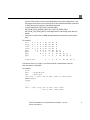
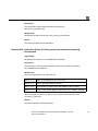
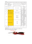
1. Errata Table
Table 1: UltraSPARC-IIe and UltraSPARC-IIi 550/650 Errata
UltraSPARC-IIe
Version 1.4
Errata #
UltraSPARC-IIi
550/650
See ...
1
D
D
page 5
2
D
D
page 7
3
D
D
page 9
4
D
D
page 10
5
D
D
page 11
6
D
D
page 12
7
D
D
page 14
8
D
D
page 15
9
D
D
page 16
10
D
D
page 18
11
D
D
page 20
12
D
D
page 22
13
D
D
page 22
14
D
D
page 23
15
D
D
page 24
16
D
D
page 25
17
D
D
page 25
18
D
D
page 25
19
D
D
page 26
20
D
D
page 27
21
D
D
page 27
Errata for UltraSPARC-IIe and UltraSPARC-IIi 550/650 - 12/12/07
Part No. 820-4005-10
3
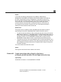
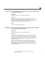
Table 1: UltraSPARC-IIe and UltraSPARC-IIi 550/650 Errata (Continued)
UltraSPARC-IIe
Version 1.4
Errata #
UltraSPARC-IIi
550/650
See ...
22
D
D
page 29
23
D
D
page 30
24
D
D
page 31
25
D
D
page 32
Errata for UltraSPARC-IIe and UltraSPARC-IIi 550/650 - 12/12/07
Part No. 820-4005-10
4
2. Errata Descriptions and Workarounds
Erratum #1:
A load from the Instruction Translation Look-Aside Buffer (ITLB) or
Data Translation Look-Aside Buffer (DTLB) may return wrong data
if the load is after a store instruction that traps or is mispredicted.
Applicability:
UltraSPARC IIe Version 1.4 and UltraSPARC IIi 550/650.
Description:
A load from the Instruction Translation Look-Aside Buffer (ITLB) or Data
Translation Look-Aside Buffer (DTLB) may return wrong data if the load is after
a store instruction to the ITLB or DTLB that traps or is mispredicted. There are
two situations in which this can happen.
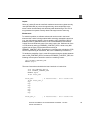
Case1: Need the following to occur:
•
Store to Address Space Identifiers (ASIs) ASI_ITLB_DATA_ACCESS or
ASI_DTLB_DATA_ACCESS_REG that traps.
•
Load from ASIs ASI_ITLB_DATA_ACCESS_REG,
ASI_DTLB_DATA_ACCESS_REG, ASI_ITLB_TAG_READ_REG,
ASI_DTLB_TAG_READ_REG.
•
No stores to Memory Management Unit (MMU) internal registers in between the
store and the load.
For example:
stxa %reg, [..]ASI ;if this instruction traps
;ASI for ITLB is 0x55 and for DTLB is 0x5d
----
;The instructions dispatched following
;store does not contain any store to MMU
;internal registers
ldxa [..]ASI, %reg ;reads TLB entry ASIs 0x55, 0x56 (for
;ITLB) ASIs 0x5d, 0x5e (for DTLB)
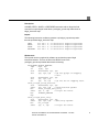
Case2: Following three conditions should be met:
•
Store to ASIs ASI_ITLB_DATA_ACCESS or ASI_DTLB_DATA_ACCESS_REG
Errata for UltraSPARC-IIe and UltraSPARC-IIi 550/650 - 12/12/07
Part No. 820-4005-10
5
(ITLB or DTLB entries) is incorrectly dispatched due to branch misprediction. This
can happen if the store is in the same group as the mispredicted branch instruction
or within the next four groups of the branch instruction.
•
Load from ASIs ASI_ITLB_DATA_ACCESS_REG
ASI_DTLB_DATA_ACCESS_REG, ASI_ITLB_TAG_READ_REG,
ASI_DTLB_TAG_READ_REG is in the target block or fall-through block after the
branch.
•
There are no other stores to MMU internal registers in between the store and the
load.
For example:
bicc
delay
inst1
inst2
grp1
grp2
grp3
grp4
F
F
F
F
D
D
D
D
F
target(ldxa)
G
G
G
G
D
F
E
E
E
E
G
D
F
C
C
C
C
E
G
D
F
N1
N1
N1
N1
C
E
G
D
N2
N2
N2
N2
N1
C
E
G
N3
N3
N3
N3
N2
N1
C
E
W
W
W
W
N3
N2
N1
C
W
N3
N2
N1
W
N3
N2
W
N3
W
F
D
G
E
C
N1
N2
N3
W
If the stxa is inst1 or in groups 1 to 4 and the branch is mispredicted, then the
ldxa can return incorrect data.
For example:
setcc
BPcc
; mispredicted
add
; delay slot
stxa %reg, [..]ASI; ASI is 0x55 (ITLB) or 0x5d (DTLB)
MEMBAR #Sync
target:
---------ldxa [..]ASI, %reg; ASI is 0x55, 0x56 (ITLB)
; ASI is 0x5D, 0x5E (DTLB)
Errata for UltraSPARC-IIe and UltraSPARC-IIi 550/650 - 12/12/07
Part No. 820-4005-10
6
Impact:
In the Instruction Memory Management Unit (I-MMU) or Data Memory
Management Unit (D-MMU), the address of the internal register to be written by
the store is latched after the store is dispatched. A wait state is entered until
the time the data is actually written. If the store instruction doesn't finish, either
due to trap (case 1) or incorrect dispatch (case 2), the control logic doesn't
reset and remains in this wait state. A subsequent load from TLB entries can
be corrupted by this wait state, resulting in the use of the address associated
with the prior store instead of that from the load.
Workaround:
The problem can be avoided by clearing the MMU wait state before the ldxa or
by preventing the stxa from dispatching until the branch resolution (case 2).
•
To clear the stxa state before the ldxa, precede the ldxa with a store to any of the
MMU internal registers (i.e., ASIs 0x50 to 0x57 for ITLB and ASIs 0x58 to 0x5F for
DTLB). Follow this store with a MEMBAR #Sync, FLUSH, or DONE instruction as
specified in section 5.3.10 "UltraSPARC-IIi Internal ASIs" on page 79 of the
UltraSPARC-IIi User's Manual. Case 1 can be fixed by this work-around only.
•
To prevent an stxa from incorrectly dispatching due to branch misprediction, use a
FLUSH (FLUSH behaves as a store) or any store instruction before stxa. The stxa
will not dispatch until the previous store is completed which will give enough time
for branch resolution.
You can use either work-around for case 2.
Status:
This bug will not be fixed in future releases of the silicon.
Erratum #2:
Certain instructions with an illegal fcn field take a
privileged_opcode trap rather than an illegal_instruction trap.
Applicability:
UltraSPARC IIe Version 1.4 and UltraSPARC IIi 550/650.
Errata for UltraSPARC-IIe and UltraSPARC-IIi 550/650 - 12/12/07
Part No. 820-4005-10
7
Description:
A DONE, RETRY, SAVED, or RESTORED instruction with an illegal fcn field
executed in nonprivileged mode takes a privileged_opcode trap rather than an
illegal_instruction trap.
Impact:
The following instruction conditions generate a privileged_opcode trap rather
than the specified illegal_instruction trap.
DONE
RETRY
SAVED
RESTORED
for
for
for
for
fcn
fcn
fcn
fcn
=
=
=
=
2..31
2..31
2..31
2..31
executed
executed
executed
executed
in
in
in
in
nonprivileged
nonprivileged
nonprivileged
nonprivileged
mode
mode
mode
mode
Workaround:
The opcode can be recognized by software to emulate the proper illegal
instruction behavior. This can be done with SPARC code in the
privileged_opcode trap handler that does the following:
PRIVILEGED_OPCODE_HANDLER:
rdpr
%tpc, %g1
ld
[%g1], %g2
setx
0xc1f80000, %g3, %g4
and
%g4, %g2, %g4
! %g4 has op/op3 of trapping
! instr.
setx
0x3e000000, %g3, %g6
and
%g6, %g2, %g6
srl
%g6, 25, %g6
! %g6 has fcn of trapping instr.
check_illegal_saved_restored:
setx
0x81880000, %g3, %g5
subcc
%g4, %g5, %g0
! saved/restored opcode?
bne
check_illegal_done_retry
subcc
%g6, 2, %g0
! illegal fcn value?
bge
ILLEGAL_HANDLER
nop
check_illegal_done_retry:
setx
0x81f00000, %g3, %g5
subcc
%g4, %g5, %g0
! done/retry opcode?
bne
not_illegal
subcc
%g6, 2, %g0
! illegal fcn value?
Errata for UltraSPARC-IIe and UltraSPARC-IIi 550/650 - 12/12/07
Part No. 820-4005-10
8
bge
ILLEGAL_HANDLER
nop
not_illegal:
<handle privileged_opcode exception as desired here>
Status:
This bug will not be fixed in future releases of the silicon.
Erratum #3:
A Jump and Link Instruction (JMPL) instruction at the boundary of
a virtual address hole sign-extends %rd.
Applicability:
UltraSPARC IIe Version 1.4 and UltraSPARC IIi 550/650.
Description:
Virtual addresses between 0x0000 0800 0000 0000 and 0xffff f7ff ffff ffff
inclusive are termed out of range. This range is referred to as the virtual
address hole and is described in Section "Virtual Address Translation" of the
UltraSPARC User’s Manual.
Impact:
The following instruction sequence causes %rd to be loaded with the wrong
value:
pc = 0x000007FF.FFFFFFFC
pc = 0x00000800.00000000
jmpl address, %rd
The %rd is saved as 0xFFFF.F800 0000 0000 when it should be the first
address in the virtual address hole 0x0000 0800 0000 0000. The failure would
been that an erroneous Jump and Link Instruction (JMPL) at the boundary
(which should trap if the correct return address was used) would create a valid
instead of invalid return address. This valid return address wouldn’t trap as a
"virtual address hole" pc.
Errata for UltraSPARC-IIe and UltraSPARC-IIi 550/650 - 12/12/07
Part No. 820-4005-10
9
Workaround:
The operating system must not map the 4 GB of instruction space immediately
above and below the virtual address hole, so the operating system would not
map the following 4 GB ranges:
lower range: 0x0000 0700 0000 0000 to 0x0000 07ff ffff ffff
upper range: 0xffff f800 0000 0000 to 0xffff f8ff ffff ffff
Since the instruction address at the boundary will never be mapped, a valid
instruction will never be executed at that pc.
Status:
This bug will not be fixed in future releases of the silicon.
Erratum #4:
A DONE or RETRY instruction with TL=0 causes a
privileged_opcode rather than an illegal_instruction trap.
Applicability:
UltraSPARC IIe Version 1.4 and UltraSPARC IIi 550/650.
Description:
A DONE or RETRY instruction with TL=0 causes a privileged_opcode rather
than an illegal_instruction trap.
Impact:
The SPARC-V9 architecture manual says an illegal_instruction trap should be
taken. Instead, a privileged_opcode trap is taken.
Workaround:
There is no workaround.
Status:
This bug will not be fixed in future releases of the silicon.
Errata for UltraSPARC-IIe and UltraSPARC-IIi 550/650 - 12/12/07
Part No. 820-4005-10
10
Erratum #5:
Traps on atomic accesses using Address Space Identifiers (ASIs)
0x5c, 0x5d, and 0x5e all cause ft[2] in the Data Memory
Management Unit (DMMU) SFSR to be set according to the Data
Translation Look-Aside Buffer (DTLB) entry.
Applicability:
UltraSPARC IIe Version 1.4 and UltraSPARC IIi 550/650.
Description:
The UltraSPARC User’s Manual says that the ft[2] bit of the Data Memory
Management Unit (DMMU) Synchronous Fault Status Register (which is
loaded on traps) is set for Atomics (including 128-bit atomic load) to a page
marked uncacheable, and that the bit is zero for internal Address Space
Identifier (ASI) accesses, except for atomics to DTLB_DATA_ACCESS_REG
(0x5D), which update according to the TLB entry accessed.
Actually, all ASI’s that access the DMMU TLB, not just 0x5D, have the same
behavior:
0x5C
0x5D
0x5E
ASI_DTLB_DATA_IN_REG
ASI_DTLB_DATA_ACCESS_REG
ASI_DTLB_TAG_READ_REG
Impact:
The documentation is incorrect.
Workaround:
The correction to the documentation is that all ASI’s that access the DMMU
TLB have the same behavior:
0x5C
0x5D
0x5E
ASI_DTLB_DATA_IN_REG
ASI_DTLB_DATA_ACCESS_REG
ASI_DTLB_TAG_READ_REG
For instance,
swapa [%g0] 0x5e, %g0
will trap with ft[3:0] = 1000 if the mapping for VA==0x0 has cp==1 and cv==1.
Errata for UltraSPARC-IIe and UltraSPARC-IIi 550/650 - 12/12/07
Part No. 820-4005-10
11
Status:
This erratum updates the documentation.
Erratum #6:
The result of a read of the Program Counter Register (PC), Trap
Program Counter Register (TPC), or Trap Next Program Counter
Register (TNPC) may not bypass correctly into subsequent
arithmetic instructions that create condition codes, causing an
incorrect setting of the V and/or C bits of CCR.xcc. A CALL or JMPL
followed by use of %o7 can cause a similar problem.
Applicability:
UltraSPARC IIe Version 1.4 and UltraSPARC IIi 550/650.
Description:
Case 1: A failing instruction sequence is:
rdpr %tpc, %i0
subcc %i0, %g2, %i3
The 65th bit of the Arithmetic Logic Unit (ALU) used in the second instruction
can be incorrect. This should only affect the setting of the V and C flags by that
instruction. It may also affect an integer divide that uses the result of the Read
Privileged Register (RDPR) instruction. (The code above might be used when
software is checking for a range of PC values and will use the V or C flag to do
a less-than, greater-than comparison.)
This problem exists if the RDPR value has 1’s in its most significant bits (it
doesn’t fail always because so much depends on bypass conditions).
Case 2: Another failing instruction sequence is a CALL or JMPL (which write to
%o7) branching to an instruction that uses %o7 and sets %ccr. A failure case
is starting at 0xffff.ffff.7f7d.0000 and an actual %o7 is 0xffff.ffff.7f7d.0008:
top:
save %sp, -192, %sp
orcc %g0, %g0, %g0
call 1f
nop
! %ccr reset
! will fail with jmpl also.
Errata for UltraSPARC-IIe and UltraSPARC-IIi 550/650 - 12/12/07
Part No. 820-4005-10
12
1:
taddcc %o7, -191, %g0
rd %ccr, %i0
! correct is 0x93. Incorrect is 0x83
ret
restore
nop
A JMPL or CALL instruction, where the register that gets the return pc is
immediately used as the source operand in an instruction that sets %ccr, can
cause the problem. (This kind of code may be present when the software
wants to compare the current Program Counter Register (PC) to some value. It
may fail intermittently, or in an on/off pattern, because of branch prediction
effects.)
Impact:
In the specified cases, the V and C bits of CCR.xcc may be set incorrectly.
Workaround:
Since the PC doesn’t have 1’s in the upper 32 bits when running in 32-bit
mode, this only occurs in 64-bit mode.
Case 1: Inhibit use of this bypass path by feeding the result of the RDPR
instruction through another operation before doing an instruction on it that sets
condition codes or integer divides. This forces a pipeline slot to be used
between the offending read and use. The example for case 1 would become:
rdpr %tpc, %i0
mov %i0,%i0
subcc %i0, %g2, %i3
Case 2: A similar workaround is feeding %o7 through itself with mov %o7, %o7
before the taddc, or inserting two nops (to consume the two integer instruction
slots).
Status:
This bug will not be fixed in future releases of the silicon.
Errata for UltraSPARC-IIe and UltraSPARC-IIi 550/650 - 12/12/07
Part No. 820-4005-10
13
Erratum #7:
An Instruction Memory Management Unit (I-MMU) miss, with a
mispredicted Delayed Control Transfer Instruction (DCTI) and
delayed issue of a delay slot, can cause instruction issue to stop.
Applicability:
UltraSPARC IIe Version 1.4 and UltraSPARC IIi 550/650.
Description:
UltraSPARC IIe and IIi can stop issuing instructions (but still be interruptible by
XIR and possibly other enabled trap conditions) due to a condition created by
an instruction sequence similar to the following:
STX
<0 or more instructions>
JMPL
MEMBAR #Sync
The Jump and Link Instruction (JMPL) can be replaced by any Delayed Control
Transfer Instruction (DCTI). When executed, the DCTI must be mispredicted
and cause an I-MMU miss. Furthermore, the delay slot instruction must be
delayed at least 8 cycles after the CTI.
A way to get an I-MMU miss is by using a predicted VA from the Return
Address Stack (RAS). An instruction like MEMBAR that waits for loads or
stores to complete may cause the significant delay needed to encounter this
problem.
Impact:
Since we can trap out of this deadlock, it is a performance loss, except when
pstate.ie==0 and timer interrupts can’t happen (e.g., trap handlers). We may
see more of this as compilers move real instructions into delay slots, rather
than NOPs.
Workaround:
Any code that turns off pstate.ie (disabling timer interrupts) or any code that is
performance sensitive and has the possibility of mispredicted JMPL or
branches with delay slots whose issue can be delayed needs to guarantee no
I-MMU miss on any predicted path for the instruction prefetch address. This
needs to be true for all behaviors of the RAS and the next-fetch random access
memory (NFRAM) in generating predicted instruction addresses.
Errata for UltraSPARC-IIe and UltraSPARC-IIi 550/650 - 12/12/07
Part No. 820-4005-10
14
For the operating system, this requires the RAS to be initialized with CALLs to
its known I-MMU-hitting VA space (i.e., CALLs that have return addresses
4 Gbytes away from the boundary of its I-MMU-hit VA space).
User code could still cause this I-MMU stop scenario. Since it's interruptible,
however, execution will resume at the next interrupt (worst case, at the time
slice), but the stop won’t be detected.
Status:
This bug will not be fixed in future releases of the silicon.
Erratum #8:
Little-endian enabled integer LDD and STD don’t register swap.
Applicability:
UltraSPARC IIe Version 1.4 and UltraSPARC IIi 550/650.
Description:
The V9 architecture requirement is given in Section 6.3.1.2.2 “Little-Endian
Addressing Convention” of The SPARC Architecture Manual, Version 9:
doubleword or extended word: For the deprecated integer load/
store double instructions (LDD/STD), two little-endian words
are accessed. The word at the address specified in the
instruction + 4 corresponds to the even register specified in
the instruction. The word at the address specified in the
instruction corresponds to the following odd-numbered
register.
Instead of this requirement, UltraSPARC-IIe and IIi always link the word
address specified in the instruction to the even register. The word address plus
4 is always linked to the odd register.
SPARC International has recently relaxed the requirement to make it
implementation-specific.
The quad load, used for Translation Look-aside Buffer (TLB) miss handling,
has a similar issue. It puts the eight bytes at [address] into the even register
and the eight bytes at [address+8] into the odd register. Each set of eight bytes
is byte-swapped:
LDDA
[address]ASI_NUCLEUS_QUAD_LDD_L, %r-even
Errata for UltraSPARC-IIe and UltraSPARC-IIi 550/650 - 12/12/07
Part No. 820-4005-10
15
behaves like:
LDXA
LDXA
[address]ASI_NUCLEUS_LITTLE, %r-even
[address+8]ASI_NUCLEUS_LITTLE, %r-even+1
Impact:
This applies to pages with the IE bit set in the TLB entry for that page, and to
the ldda and stda instructions used with any of the "LITTLE" Address Space
Identifiers (ASIs), such as:
ASI_AS_IF_USER_PRIMARY_LITTLE
ASI_AS_IF_USER_SECONDARY_LITTLE
ASI_NUCLEUS_LITTLE
ASI_PRIMARY_LITTLE
ASI_SECONDARY_LITTLE
ASI_SECONDARY_NOFAULT_LITTLE
Status:
This erratum updates the documentation.
Erratum #9:
A floating-point store instruction doesn’t synchronize on a block
load data return without an intervening floating point operate
instruction.
Applicability:
UltraSPARC IIe Version 1.4 and UltraSPARC IIi 550/650.
Description:
The first instruction group after a second block load is always stalled,
regardless of what instruction it is, until you get the first piece of data back from
the first block load. After that and the next instruction group issue, the FP
instruction group issue is supposed to throttle based on availability of data (if
data comes back 8 bytes every cycle, there is no throttling). However, this
secondary throttling doesn't occur if the instructions are floating-point store and
the floating-point stores issue every cycle, regardless of when the remaining
block load data arrives.
Errata for UltraSPARC-IIe and UltraSPARC-IIi 550/650 - 12/12/07
Part No. 820-4005-10
16
Impact:
The value written by the floating-point store instruction may be either the old
value of the register or the value from the preceding block load instruction.
Workaround:
The following rules supersede the ones found in the description of the block
load/store instructions on pages 174-176 of the UltraSPARC-IIi User's Manual.
Block load does not provide register dependency interlocks like ordinary load
instructions.
Before referencing block load data, a second block load (to a different set of
registers) or a MEMBAR #Sync must be performed. If a second block load is
used to synchronize against returning data, UltraSPARC will continue
execution before all data has been returned. The programmer is then
responsible for scheduling instructions so registers are only used when they
become valid.
To determine when data is valid, the programmer must count instruction
groups containing FP operate instructions (not FP loads or stores). The lowest
number register being loaded by the first block load may be referenced in the
first instruction group following the second block load, using an FP operate
instruction only.
The second lowest number register may be referenced in the second
instruction group containing an FP operate instruction, and so on. The best
case grouping of FP operates should be assumed (i.e., issuing any M-Class FP
operation in the same group as any possible A-Class FP operation).
(UltraSPARC can issue two FP operate instructions simultaneously, assuming
they are in different classes.)
If this dual block load synchronization mechanism is used, the initial reference
to the block load data must be an FP operate instruction (not a FP store), and
only instruction groups with FP operate instructions are counted when
determining block load data availability.
If these rules are violated, data from before or after the block load may be
returned.
If a MEMBAR #Sync is used to synchronize on block load data, there are no
restrictions on data usage, although this will be lower performance. No other
MEMBAR's can be used to provide data synchronization for a block load.
Errata for UltraSPARC-IIe and UltraSPARC-IIi 550/650 - 12/12/07
Part No. 820-4005-10
17
FP operate instructions can be issued in a single group with FP stores. If dual
block load synchronization is used, FP operates and FP stores can be
interlaced. This allows a FP operate to reference the returning data before
using the data in any FP store (normal store, or block store).
Typically, the FP operate instruction will be a Floating Point Move Double
(FMOVD) or Data Alignment in Floating Point Graphics Adder (FALIGNDATA).
UltraSPARC also continues execution, without register interlocks, before all the
the store data for block stores is transferred from the register file.
If store data registers are overwritten before the next block store or MEMBAR
#Sync instruction, then the following rule must be observed: The first register
can be overwritten in the same instruction group as the block store, the second
register can be overwritten in the instruction group following the block store,
and so on. If this rule is violated, the store may use the old or the new
overwritten data.
When determining correctness for a code sample, be aware that UltraSPARC
implementations may interlock more than required above. There may be partial
register interlocks (for instance on the lowest number register).
Code that doesn't meet the above constraints may appear to work on a
particular platform. However, to be portable across all UltraSPARC
implementations, all of the above rules must be followed.
Status:
This erratum updates the documentation.
Erratum #10: Clarification on manipulation of the Used bit in the Instruction
Translation Look-Aside Buffer (iTLB) and Data Translation LookAside Buffer (dTLB).
Applicability:
UltraSPARC IIe Version 1.4 and UltraSPARC IIi 550/650.
Errata for UltraSPARC-IIe and UltraSPARC-IIi 550/650 - 12/12/07
Part No. 820-4005-10
18
Description:
The Data Translation Look-Aside Buffer (dTLB) and Instruction Translation
Look-aside Buffer (iTLB) support a least-recently-used (LRU) replacement
algorithm. When software does a write of the I/D-TLB Data In Registers using
Address Space Identifier (ASI) 0x54 or 0x5C, the entry used for the write is
selected depending on the state of the Lock, Used, and Valid bits in the TLB.
The Used bit is set to 1 each time an entry is accessed for a translation.
The description of how the hardware selects an entry, and how the Used bits
are cleared, is not accurate enough in the User’s Manual. Ordinarily the exact
behavior of the Used bits is not of interest to software, so this is only of interest
in understanding the hardware.
Impact:
There is a case where software, if it tried to set the Used bit to 1, could result in
an indeterminate value in the Used bit. This could cause "lock-step" CPUs to
get out of sync, since the Used bit manipulations have to be exactly the same
for two CPUs to operate identically.
Workaround:
Software should never write Used==1 (bit 0 of the Diag field, which is bit 41 of
the Data In register), using Data In writes because if a clear of the Used bits is
being done in the same cycle by hardware, the results are indeterminate.
There is no such constraint on Data Access writes.
The exact least-recently-used (LRU) selection algorithm is:
if (there exists x : x.v == 0) {
first such x;
} elseif (there exists y: y.u == 0 && y.l == 0) {
first such y;
} elseif (there exists z: z.l == 0) {
first such z;
} else {
entry 63;
}
Errata for UltraSPARC-IIe and UltraSPARC-IIi 550/650 - 12/12/07
Part No. 820-4005-10
19
A hardware u-clear (i.e., clear of all the used bits) can be triggered in just about
any TLB cycle, even if the TLB is doing say a write. A u-clear is triggered when
all entries are valid and none have Lock==0 and Used==0. So, for example,
locking an entry that never gets the Used bit set won’t inhibit the u-clear
operation.
Status:
This erratum updates the documentation.
Erratum #11: Clarification on the use of CP==1, CV==0 (e.g., ASI_PHYS_USE_EC)
to bypass the Data Cache (D-cache).
Applicability:
UltraSPARC IIe Version 1.4 and UltraSPARC IIi 550/650.
Description:
The Data Cache (D-cache) can return stale data if CP==1, CV==0 is used to
bypass the cache after using CP==1 and CV==1 for loads and stores to a
particular address.
The term "noncacheable" in the User’s Manual does not refer to "non-Dcacheable". The term "virtually noncacheable" does refer to the "non-Dcacheable" CP==1, CV==0 case.
CP==1,
CP==1,
CP==0,
CP==0,
CV==1:
CV==0:
CV==1:
CV==0:
Cacheable, Virtually-cacheable
Cacheable, Virtually-noncacheable
Not Used
Noncacheable
Impact:
Q: When I do a load with a physical address, using ASI=0x14
(ASI_PHYS_USE_EC), causing CP==1 and CV==0, and the address hits in
the D-cache, does the data come from Dcache instead of E-cache?
Errata for UltraSPARC-IIe and UltraSPARC-IIi 550/650 - 12/12/07
Part No. 820-4005-10
20
A: The UltraSPARC-IIi User's Manual (section 3.1.1.2) has a caveat that is
similar to this case: If CP==0 and CV==0, which indicates a "noncacheable"
access, and the address is in the D-cache, data can be returned from the Dcache. The manual warns that the address should be flushed from the D-cache
before changing it’s mapping.
Similarly, if CP==1, and CV==0, and the data is in the D-cache, data may be
returned from the Dcache.
However there are corner cases where it may not be. For instance, with
ASI_PHYS_USE_EC, the physical PA[13] is used to index the D-cache, where
Virtual Address VA[13] would ordinarily be used. So the Dcache data would not
be returned if the real valid data was in VA[13]==0, but PA[13]==1. Ordinarily
the rest of the PA bits will have a difference, so you’ll miss in the D-cache and
go to the E-cache correctly. This takes advantage of knowing that a valid PA
can only exist in one VA[13] mapping at a time in the D-cache. This depends
on how the addresses were mapped earlier, when the line was installed in the
D-cache.
This ASI_PHYS_USE_EC load hitting on the D-cache behavior is not defined
or tested, so software should not rely on it.
Q: When I do a store with a physical address, using ASI=0x14
(ASI_PHYS_USE_EC), causing CP==1 and CV==0, and the address hits in
the D-cache, does the D-cache get updated?
A: It may, but this behavior is not verified or guaranteed. Again, software
should make sure the physical address is not in the D-cache before accessing
that address using CP==1, CV==0, whether by a Translation Look-Aside Buffer
(TLB) mapping, or using one of the special ASIs.
Workaround:
The D-cache should be flushed, after mixing use of any CP/CV settings for a
physical address, including cacheable (DRAM) and noncacheable Input/Output
(IO) physical addresses.
Only two entries in the dcache need be flushed for each physical address
{VA[13]==0,PA[12:0]} and {VA[13]==1,PA[12:0]}.
Status:
This erratum updates the documentation.
Errata for UltraSPARC-IIe and UltraSPARC-IIi 550/650 - 12/12/07
Part No. 820-4005-10
21
Erratum #12: The IP, DV, DP, CD bits aren’t documented in the Load/Store Unit
(LSU) Control Register.
Applicability:
UltraSPARC IIe Version 1.4 and UltraSPARC IIi 550/650.
Description:
•
Bit 43 is the default D-MMU physical cacheability (D-MMU CP) bit. This bit is used
when the D-MMU is disabled.
•
Bit 42 is the default D-MMU virtual cacheability (D-MMU CV) bit. This bit is used
when the D-MMU is disabled.
•
Bit 41 is the default I-MMU physical cacheability (I-MMU CP) bit. This bit is used
when the I-MMU is disabled.
•
Bit 20 is the CD bit. This bit disables store compression by the store buffer when
set.
These bits are reset to 0 and should normally always be written with 0.
Status:
This erratum updates the documentation.
Erratum #13: A Memory Barrier Instruction (MEMBAR) is sometimes needed after
using ASI_PHYS_USE_EC* with a store.
Applicability:
UltraSPARC IIe Version 1.4 and UltraSPARC IIi 550/650.
Description:
A read-after-write (RAW) hazard occurs when a READ transaction has an
address match with a pending WRITE entry address. UltraSPARC's RAW
hazard detection logic uses bits 13:4. For ordinary loads and stores, bit 13 is
VA<13>. However, when ASI_PHYS_USE_EC{_LITTLE} (ASI 0x14 or 0x1C) is
used, bit 13 is PA<13>.
Errata for UltraSPARC-IIe and UltraSPARC-IIi 550/650 - 12/12/07
Part No. 820-4005-10
22
Impact:
If you do a store using ASI_PHYS_USE_EC{_LITTLE} with PA<13> of one
value and then follow immediately with a normal load with VA<13> of another
value (but which maps to the same PA), the RAW hazard will not be detected
and the load may get a stale value. The same problem occurs for an ordinary
store followed by a load with ASI_PHYS_USE_EC{_LITTLE}.
A similar case arises in relaxed memory order (RMO) for loads followed by
stores. In RMO, stores may be performed before earlier loads, so long as they
are to different locations. The write-after-read (WAR) check again relies on
<13> of the address. When VA<13> and PA<13> for the same location have
different values, it is possible that an earlier load would return the value from
the later store.
Workaround:
If accesses to a particular location involve a mixture of normal (VA) and
ASI_PHYS_USE_EC{_LITTLE} and system software doesn't guarantee that
VA<13> == PA<13>, then the following rules need to be followed:
•
Add MEMBAR #StoreLoad following each store with
ASI_PHYS_USE_EC{_LITTLE}.
•
Add MEMBAR #StoreLoad prior to each load with ASI_PHYS_USE_EC{_LITTLE}.
•
In RMO mode, add MEMBAR #LoadStore following each load with
ASI_PHYS_USE_EC{_LITTLE}.
•
In RMO mode, add MEMBAR #LoadStore prior to each store with
ASI_PHYS_USE_EC{_LITTLE}.
Status:
This bug will not be fixed in future releases of the silicon.
Erratum #14: The Instruction Memory Management Unit (IMMU) and Data Memory
Management Unit (DMMU) Synchronous Fault Status Register
(SFSR) Fault Valid (FV) bit is not reset to zero at power-on reset
(POR).
Applicability:
UltraSPARC IIe Version 1.4 and UltraSPARC IIi 550/650.
Errata for UltraSPARC-IIe and UltraSPARC-IIi 550/650 - 12/12/07
Part No. 820-4005-10
23
Description:
The User’s Manual says that the Instruction Memory Management Unit (IMMU)
and Data Memory Management Unit (DMMU) Synchronous Fault Status
Register (SFSR) Fault Valid (FV) bit should be zero at power-on reset (POR).
There is no logic that does this reset, so the bit is unknown at power-on reset
like the rest of the SFSR.
Impact:
Software must already zero this bit at powerup, so there should be no impact.
Workaround:
The software must zero this bit at powerup.
Status:
This erratum updates the documentation.
Erratum #15: The Synchronous Fault Status Register (SFSR) E-bit is not set
properly for some exceptions with
ASI_PHYS_BYPASS_EC_WITH_EBIT{_LITTLE} (0x15 or 0x1D).
Applicability:
UltraSPARC IIe Version 1.4 and UltraSPARC IIi 550/650.
Description:
The Synchronous Fault Status Register (SFSR) E-bit should normally be set to
1 whenever a faulting access occurs using
ASI_PHYS_BYPASS_EC_WITH_EBIT{_LITTLE} (0x15 and 0x1D).
However, if the address is within the VA "hole" (i.e., 0x0000080000000000 to
0xfffff7ffffffffff) and a precise trap occurs (including mem_address_not_aligned
and privileged_action), SFSR.E will be set to 0, not 1.
Status:
This bug will not be fixed in future releases of the silicon.
Errata for UltraSPARC-IIe and UltraSPARC-IIi 550/650 - 12/12/07
Part No. 820-4005-10
24
Erratum #16: The Dispatch Control Register is Ancillary State Register (ASR) 18
decimal, not 18 hexadecimal.
Applicability:
UltraSPARC IIe Version 1.4 and UltraSPARC IIi 550/650.
Description:
The UltraSPARC User’s Manual says that the Ancillary State Register (ASR)
for the Dispatch Control Register is 18 hexadecimal. This is incorrect. It is 18
decimal (12 hexadecimal).
Status:
This erratum updates the documentation.
Erratum #17: ASI_PHYS_USE_EC{_LITTLE} is incorrectly documented as
unrestricted.
Applicability:
UltraSPARC IIe Version 1.4 and UltraSPARC IIi 550/650.
Description:
Table 8-1 in section 8.3.3 of the UltraSPARC IIi User’s Manual incorrectly lists
ASI_PHYS_USE_EC{_LITTLE} as unrestricted.
ASI_PHYS_USE_EC{_LITTLE} is restricted.
Status:
This erratum updates the documentation.
Erratum #18: The documentation incorrectly mentions data_access_protection
rather than fast_data_access_protection.
Applicability:
UltraSPARC IIe Version 1.4 and UltraSPARC IIi 550/650.
Errata for UltraSPARC-IIe and UltraSPARC-IIi 550/650 - 12/12/07
Part No. 820-4005-10
25
Description:
The UltraSPARC User’s Manual incorrectly mentions the
data_access_protection trap.
Workaround:
UltraSPARC actually uses the fast_data_access_protection trap.
Status:
This erratum updates the documentation.
Erratum #19: Instruction Cache (I-Cache) predecode values are incorrectly
documented.
Applicability:
UltraSPARC IIe Version 1.4 and UltraSPARC IIi 550/650.
Description:
The Instruction Cache (I-Cache) predecode values are incorrectly described in
the UltraSPARC User’s Manual.
Workaround:
The correct descriptions of IC_pdec bits are:
Bit<3> == 1
JMPL or RETURN with rs1==%o7 or %i7
Bit<2> == 1
JMPL, RETURN, DONE or RETRY
Bit<1> == 0
A PC-relative CTI (BPcc, Bicc, BPr, FBPfcc, FBfcc or CALL)
Bit<0> == 0
CALL, or the "branch always" case of BPcc, Bicc, FBPfcc, or FBfcc
When clearing the I-Cache (e.g., after a reset), software should write the value
3 to each IC_pdec field.
Status:
This erratum updates the documentation.
Errata for UltraSPARC-IIe and UltraSPARC-IIi 550/650 - 12/12/07
Part No. 820-4005-10
26
Erratum #20: The sign of floating-point subnormal results in non-standard mode
is incorrectly documented.
Applicability:
UltraSPARC IIe Version 1.4 and UltraSPARC IIi 550/650.
Description:
The sign of floating-point subnormal results with Floating-Point Status Register
(FSR.NS)=1 are incorrectly described in the section 14.3.1.1 of the
UltraSPARC-IIi User's Manual. The result is always a positive zero (rather than
zero with the same sign as incorrectly stated in the manual).
Status:
This erratum updates the documentation.
Erratum #21: Enabling Instruction Cache (I-cache) may put the same tag in both
sets, causing unexpected behavior.
Applicability:
UltraSPARC IIe Version 1.4 and UltraSPARC IIi 550/650.
Description:
There are two internal signals which enable the Instruction Cache (I-cache).
One enables I-cache writes and the other enables I-cache tag comparisons for
reads. The first one is delayed until the I-cache fill machine reaches the idle
state. The second one is delayed until the next time the uTLB (micro-TLB) is
reloaded from the I-TLB.
When turning on the I-cache by writing 1 to the Load/Store Unit Control
Register (LSU_CONTROL_REG.IC), I-cache writes may be enabled much
earlier than the I-cache tag comparators. So while the tag comparators are
reporting I-cache misses, the corresponding instruction fills are actually being
written to I-cache as valid.
Errata for UltraSPARC-IIe and UltraSPARC-IIi 550/650 - 12/12/07
Part No. 820-4005-10
27
Impact:
Since an I-cache fill sets the next-fetch random access memory least recently
used (NFRAM.LRU) to point to the opposite way, these multiple fills to the
same I-cache line alternately write both ways with identical tags. The CPU is
not guaranteed to operate correctly when both ways have the same tag.
Workaround:
To avoid this problem, a software workaround can be made in the kernel
whenever the I-cache is being enabled while executing cacheable instructions
(e.g., the deferred trap handler). After re-enabling LSU_CONTROL_REG.IC,
software needs to guarantee that the uTLB is reloaded before two identical
I-cache fills could write both ways of the same I-cache line. Software can force
a uTLB reload by writing to PRIMARY_CONTEXT_REG. A write to any IMU
register has the same uTLB reload effect as writing to
PRIMARY_CONTEXT_REG. (Branching to a new page also reloads the uTLB,
but due to prefetching of instructions, this is not a satisfactory workaround.)
To handle the possibility of two I-cache fill requests during the window between
stxa to LSU_CONTROL_REG.IC and stxa to PRIMARY_CONTEXT_REG, the
following code sequence should be used for re-enabling I-cache:
ldxa PRIMARY_CONTEXT_REG
MEMBAR #Sync
The next 4 instructions should be the last 4 words in an I-cache line:
stxa LSU_CONTROL_REG.IC
stxa PRIMARY_CONTEXT_REG
MEMBAR #Sync
flush flush_adr
flush_adr:
; 8 instructions - one I-cache line
flush flush_adr_2
nop
nop
nop
nop
nop
nop
nop
flush_adr_2:
; 8 instructions - one I-cache line
Errata for UltraSPARC-IIe and UltraSPARC-IIi 550/650 - 12/12/07
Part No. 820-4005-10
28
nop
nop
nop
nop
nop
nop
nop
retry
The nops could be replaced by useful code, such as restoring registers from
memory. Hardware prefetching will continue while the MEMBAR #Sync is
waiting on the stxa to PRIMARY_CONTEXT_REG. Since the IBuffer has only
12 entries and there are more than 12 instructions before the retry, this
ensures that hardware prefetching will not continue past the retry. To be extra
careful, the trap handler only has to worry about duplicate fills for flush_adr and
flush_adr_2. Flushing these two I-cache lines will prevent any future multi-way
I-cache hits.
Status:
This bug will not be fixed in future releases of the silicon.
Erratum #22: A prefetch fcn 1, 2, 3 or 4 may cause the wrong data to be used for
the %g[1-4] operand of a later instruction.
Applicability:
UltraSPARC IIe Version 1.4 and UltraSPARC IIi 550/650.
Description:
A prefetch instruction is handled very much like a load instruction and the fcn
field occupies the same bits of the prefetch instruction that are used as the
destination register in the load instruction. If the Load/Store Unit (LSU) is in
delayed return mode due to an earlier signed load and the prefetch happens to
be completing at the same time that a later instruction uses the appropriate %g
register (the one that matches the fcn of the prefetch) as a source register,
then the register bypass logic incorrectly selects the annex register file as the
source of the data instead of the Integer Core Register File (ICRF).
Errata for UltraSPARC-IIe and UltraSPARC-IIi 550/650 - 12/12/07
Part No. 820-4005-10
29
Impact:
When the fcn of a prefetch is 1, 2, 3 or 4 and the corresponding %g register
appears as the source operand of a later instruction, the annex data for the %g
register may be incorrectly bypassed to the operand of the later instruction.
Workaround:
There are three workarounds available:
1. Do not use a prefetch with fcn 1, 2, 3 or 4. Instead, use fcn 0 for similar functionality
or use fcn 20-23 (treated as a no-op).
2. Make sure there is a load to a different register following the prefetch and a use of
that register before the instruction that uses the %g register (this works because
prefetches and loads complete in order).
3. Add a Memory Barrier Instruction (MEMBAR) #Sync between the prefetch and the
instruction that uses the %g register (this incurs a performance penalty).
A deferred trap waits for outstanding prefetches to complete, so deferred trap
handlers need not worry about this erratum.
Status:
This bug will not be fixed in future releases of the silicon.
Erratum #23: The MVX bit in the Dispatch Control Register can cause incorrect
results.
Applicability:
UltraSPARC IIe Version 1.4 and UltraSPARC IIi 550/650.
Description:
Section I.1.2 of the UltraSPARC-IIi User's Manual says that the MVX bit is in
position 2, but it is really in position 1. In addition, the manual says that this bit
enables a performance improvement for the MOVX instruction, but this
optimization does not work correctly.
Impact:
This MOVX instruction optimization can cause incorrect values to be used for
registers following branch instructions.
Errata for UltraSPARC-IIe and UltraSPARC-IIi 550/650 - 12/12/07
Part No. 820-4005-10
30
Workaround:
System software must always set the MVX bit (bit 1) in the Dispatch Control
Register (ASR 18) to 0.
Status:
This bug will not be fixed in future releases of the silicon.
Erratum #24: A noncacheable load or store using Physical Address PA[40:0] that
maps to the unused PCI Bus Module (PBM) PCI Configuration
Space (function!=0) may result in hang.
Applicability:
UltraSPARC IIe Version 1.4 and UltraSPARC IIi 550/650.
Description:
The 2.1 PCI spec says that references to any unused configuration space
should be a no-op, but there are two situations that may hang the processor.
Impact:
The first is an illegal case: a noncacheable load or store with Physical Address
PA[40:0] in the range 0x1FE.0100.0100–0x1FE.0100.07FF and the ASI is 0x77
or 0x7F (SDB Control Status Registers [CSRs]). Normally, unspecified
addresses like this can alias to other CSRs.
The second case is a noncacheable load or store to the range
0x1FE.0100.0100–0x1FE.0100.07FF. This is the PCI Bus Module’s (PBM’s)
PCI configuration space for function!=0. The PBM has no valid CSRs for
nonzero function ID.
Both of these cases may cause the processor to hang.
Workaround:
Avoid doing a noncacheable load or store to this address space.
Status:
This bug will not be fixed in future releases of the silicon.
Errata for UltraSPARC-IIe and UltraSPARC-IIi 550/650 - 12/12/07
Part No. 820-4005-10
31
Erratum #25: The documentation does not indicate how the operating system
can recognize the processor.
Applicability:
UltraSPARC IIe Version 1.4 and UltraSPARC IIi 550/650.
Workaround:
Read the values of the VER.impl and VER.mask fields (VER.impl identifies the
implementation of the SPARC architecture and VER.mask specifies current
mask set revision):
•
UltraSPARC IIe: VER.impl = 0x13 and VER.mask = 0x14 for version 1.4.
•
UltraSPARC IIi: VER.impl = 0x13 and VER.mask = 0x13 for version 1.3.
Status:
This erratum updates the documentation.
Errata for UltraSPARC-IIe and UltraSPARC-IIi 550/650 - 12/12/07
Part No. 820-4005-10
32