1
microSPARC™-IIep
User’s Manual
April 1997
-
microSPARC-IIep User’s Manual
April 1997
Sun Microelectronics
2550 Garcia Avenue
Mountain View, CA U.S.A. 94043
1-800-681-8845
www.sun.com/sparc
Part Number: 802-7100-01
Copyright © 1997 Sun Microelectronics All Rights Reserved.
THE INFORMATION CONTAINED IN THIS DOCUMENT IS PROVIDED “AS
IS” WITHOUT ANY EXPRESS REPRESENTATIONS OR WARRANTIES. IN
ADDITION, SUN MICROELECTRONICS DISCLAIMS ALL IMPLIED
REPRESENTATIONS AND WARRANTIES, INCLUDING ANY WARRANTY OF
MERCHANTABILITY, FITNESS FOR A PARTICULAR PURPOSE, OR NONINFRINGEMENT OF THIRD PARTY INTELLECTUAL PROPERTY RIGHTS.
This document contains proprietary information of Sun Microelectronics or under
license from third parties. No part of this document may be reproduced in any
form or by any means or transferred to any third party without the prior written
consent of Sun Microelectronics
Sun, Sun Microsystems, and the Sun logo are trademarks or registered
trademarks of Sun Microelectronics in the United States and other countries. All
SPARC trademarks are used under license and are trademarks or registered
trademarks of SPARC International, Inc. in the United States and other countries.
Products bearing SPARC trademarks are based upon an architecture developed
by Sun Microelectronics
The information contained in this document is not designed or intended for use
in on-line control of aircraft, air traffic, aircraft navigation or aircraft
communications; or in the design, construction, operation or maintenance of any
nuclear facility. Sun disclaims any express or implied warranty of fitness for such
uses.
Printed in the United States of America.
Contents
1. microSPARC-IIep Overview . . . . . . . . . . . . . . . . . . . . . . . . . . . . . . . . . . . . . . .
1.1 Introduction . . . . . . . . . . . . . . . . . . . . . . . . . . . . . . . . . . . . . . . . . . . . . . . . .
1.2 microSPARC-IIep Memory Map . . . . . . . . . . . . . . . . . . . . . . . . . . . . . . . .
1.3 Endian Support . . . . . . . . . . . . . . . . . . . . . . . . . . . . . . . . . . . . . . . . . . . . . .
1.3.1 Processor-to-System Memory Endian Conversion. . . . . . . . . . .
1.3.2 Processor-to-PCI Endian Conversion. . . . . . . . . . . . . . . . . . . . . .
1.3.3 Settings for Endian Conversion . . . . . . . . . . . . . . . . . . . . . . . . . .
1.3.3.1 Big Endian Environment . . . . . . . . . . . . . . . . . . . . . . . .
1.3.3.2 Little Endian Environment . . . . . . . . . . . . . . . . . . . . . .
1.4 Block Diagram . . . . . . . . . . . . . . . . . . . . . . . . . . . . . . . . . . . . . . . . . . . . . . .
1
1
3
4
4
6
7
7
8
8
2. CPU Performance. . . . . . . . . . . . . . . . . . . . . . . . . . . . . . . . . . . . . . . . . . . . . . . . .
2.1 Benchmark Test Results . . . . . . . . . . . . . . . . . . . . . . . . . . . . . . . . . . . . . . .
2.1.1 Benchmark Test Setup . . . . . . . . . . . . . . . . . . . . . . . . . . . . . . . . . .
2.1.2 SPECint92 Test Results . . . . . . . . . . . . . . . . . . . . . . . . . . . . . . . . .
2.1.3 SPECfp92 Test Results . . . . . . . . . . . . . . . . . . . . . . . . . . . . . . . . . .
2.1.4 Dhrystone Test Results . . . . . . . . . . . . . . . . . . . . . . . . . . . . . . . . .
2.2 Compiler Optimization Guidelines . . . . . . . . . . . . . . . . . . . . . . . . . . . . .
2.2.1 Branches . . . . . . . . . . . . . . . . . . . . . . . . . . . . . . . . . . . . . . . . . . . . .
2.2.2 Guidelines for Branch Folding . . . . . . . . . . . . . . . . . . . . . . . . . . .
2.2.3 Multicycle Instructions . . . . . . . . . . . . . . . . . . . . . . . . . . . . . . . . .
2.2.4 Pipeline Interlocks . . . . . . . . . . . . . . . . . . . . . . . . . . . . . . . . . . . . .
11
11
12
12
13
13
13
13
14
16
17
microSPARC-IIep User’s Manual — April 1997
i
2.2.5
2.2.6
Other Guidelines . . . . . . . . . . . . . . . . . . . . . . . . . . . . . . . . . . . . . .
Floating-Point Instructions . . . . . . . . . . . . . . . . . . . . . . . . . . . . . .
2.2.6.1 FP Interlocks . . . . . . . . . . . . . . . . . . . . . . . . . . . . . . . . . .
2.2.6.2 Functional Units . . . . . . . . . . . . . . . . . . . . . . . . . . . . . . .
2.2.6.3 FP Queue Details . . . . . . . . . . . . . . . . . . . . . . . . . . . . . .
2.2.7 Loads and Stores . . . . . . . . . . . . . . . . . . . . . . . . . . . . . . . . . . . . . .
2.2.8 General Techniques . . . . . . . . . . . . . . . . . . . . . . . . . . . . . . . . . . . .
Using the Two Page-Hit Registers . . . . . . . . . . . . . . . . . . . . . . . . . . . . . .
17
17
18
18
18
21
22
22
3. Integer Unit. . . . . . . . . . . . . . . . . . . . . . . . . . . . . . . . . . . . . . . . . . . . . . . . . . . . . .
3.1 Overview . . . . . . . . . . . . . . . . . . . . . . . . . . . . . . . . . . . . . . . . . . . . . . . . . . .
3.2 Instruction Pipeline . . . . . . . . . . . . . . . . . . . . . . . . . . . . . . . . . . . . . . . . . .
3.3 Memory Operations . . . . . . . . . . . . . . . . . . . . . . . . . . . . . . . . . . . . . . . . . .
3.3.1 Loads . . . . . . . . . . . . . . . . . . . . . . . . . . . . . . . . . . . . . . . . . . . . . . . .
3.3.2 Stores . . . . . . . . . . . . . . . . . . . . . . . . . . . . . . . . . . . . . . . . . . . . . . . .
3.3.3 Atomic Operations . . . . . . . . . . . . . . . . . . . . . . . . . . . . . . . . . . . . .
3.4 ALU/Shift Operations . . . . . . . . . . . . . . . . . . . . . . . . . . . . . . . . . . . . . . . .
3.5 Integer Multiply . . . . . . . . . . . . . . . . . . . . . . . . . . . . . . . . . . . . . . . . . . . . .
3.6 Integer Divide . . . . . . . . . . . . . . . . . . . . . . . . . . . . . . . . . . . . . . . . . . . . . . .
3.7 Control-Transfer Instructions . . . . . . . . . . . . . . . . . . . . . . . . . . . . . . . . . .
3.7.1 Branches . . . . . . . . . . . . . . . . . . . . . . . . . . . . . . . . . . . . . . . . . . . . .
3.7.2 JMPL . . . . . . . . . . . . . . . . . . . . . . . . . . . . . . . . . . . . . . . . . . . . . . . .
3.7.3 RETT . . . . . . . . . . . . . . . . . . . . . . . . . . . . . . . . . . . . . . . . . . . . . . . .
3.7.4 CALL . . . . . . . . . . . . . . . . . . . . . . . . . . . . . . . . . . . . . . . . . . . . . . . .
3.8 Instruction Cache Interface . . . . . . . . . . . . . . . . . . . . . . . . . . . . . . . . . . . .
3.9 Data Cache Interface. . . . . . . . . . . . . . . . . . . . . . . . . . . . . . . . . . . . . . . . . .
3.10 Interlocks . . . . . . . . . . . . . . . . . . . . . . . . . . . . . . . . . . . . . . . . . . . . . . . . . . .
3.10.1 Load Interlock. . . . . . . . . . . . . . . . . . . . . . . . . . . . . . . . . . . . . . . . .
3.10.2 Floating Point Interlocks . . . . . . . . . . . . . . . . . . . . . . . . . . . . . . . .
3.10.3 Miscellaneous Interlocks . . . . . . . . . . . . . . . . . . . . . . . . . . . . . . . .
3.11 Traps and Interrupts . . . . . . . . . . . . . . . . . . . . . . . . . . . . . . . . . . . . . . . . . .
3.11.1 Traps. . . . . . . . . . . . . . . . . . . . . . . . . . . . . . . . . . . . . . . . . . . . . . . . .
3.11.2 Interrupts. . . . . . . . . . . . . . . . . . . . . . . . . . . . . . . . . . . . . . . . . . . . .
3.11.3 Reset Trap . . . . . . . . . . . . . . . . . . . . . . . . . . . . . . . . . . . . . . . . . . . .
25
25
27
28
28
30
30
31
32
32
33
33
34
35
35
35
36
36
36
36
37
37
37
38
39
2.3
ii
microSPARC-IIep User’s Manual — April 1997
3.11.4 Error Mode . . . . . . . . . . . . . . . . . . . . . . . . . . . . . . . . . . . . . . . . . . . 40
3.12 Floating-Point Interface . . . . . . . . . . . . . . . . . . . . . . . . . . . . . . . . . . . . . . . 40
3.13 Compliance With SPARC Version 8 . . . . . . . . . . . . . . . . . . . . . . . . . . . . . 41
4. Floating-Point Unit . . . . . . . . . . . . . . . . . . . . . . . . . . . . . . . . . . . . . . . . . . . . . . .
4.1 Overview . . . . . . . . . . . . . . . . . . . . . . . . . . . . . . . . . . . . . . . . . . . . . . . . . . .
4.2 Deviations from SPARC version 8 . . . . . . . . . . . . . . . . . . . . . . . . . . . . . .
4.3 Implementation Specific Features . . . . . . . . . . . . . . . . . . . . . . . . . . . . . . .
4.3.1 fp_execute State . . . . . . . . . . . . . . . . . . . . . . . . . . . . . . . . . . . . . . .
4.3.2 fp_exception_pending State . . . . . . . . . . . . . . . . . . . . . . . . . . . . .
4.3.3 fp_exception State . . . . . . . . . . . . . . . . . . . . . . . . . . . . . . . . . . . . .
4.3.4 STDFQ Instruction . . . . . . . . . . . . . . . . . . . . . . . . . . . . . . . . . . . . .
4.4 Software Considerations . . . . . . . . . . . . . . . . . . . . . . . . . . . . . . . . . . . . . .
4.5 FP Performance Factors . . . . . . . . . . . . . . . . . . . . . . . . . . . . . . . . . . . . . . .
43
44
49
50
51
51
52
52
52
54
5. Memory Management Unit . . . . . . . . . . . . . . . . . . . . . . . . . . . . . . . . . . . . . . . .
5.1 Overview . . . . . . . . . . . . . . . . . . . . . . . . . . . . . . . . . . . . . . . . . . . . . . . . . . .
5.2 MMU Programming Interface . . . . . . . . . . . . . . . . . . . . . . . . . . . . . . . . . .
5.3 Reference MMU Registers (ASI=0x04) . . . . . . . . . . . . . . . . . . . . . . . . . . .
5.3.1 Processor Control Register (VA[12:8]=0x00) . . . . . . . . . . . . . . . .
5.3.2 Context Table Pointer Register (VA[12:8]=0x01). . . . . . . . . . . . .
5.3.3 Context Register (VA[12:8]=0x02) . . . . . . . . . . . . . . . . . . . . . . . .
5.3.4 Synchronous Fault Status Register (VA[12:8]=0x03,
VA[12:8]=0x13) . . . . . . . . . . . . . . . . . . . . . . . . . . . . . . . . . . . . . . . .
5.3.5 Synchronous Fault Address Register (VA[12:8]=0x04,
VA[12:8]=0x14) . . . . . . . . . . . . . . . . . . . . . . . . . . . . . . . . . . . . . . . .
5.3.6 TLB Replacement Control Register (VA[12:8]=0x10) . . . . . . . . .
5.4 TLB Table Walk . . . . . . . . . . . . . . . . . . . . . . . . . . . . . . . . . . . . . . . . . . . . . .
5.5 Translation Lookaside Buffer (TLB) . . . . . . . . . . . . . . . . . . . . . . . . . . . . .
5.5.1 TLB Replacement . . . . . . . . . . . . . . . . . . . . . . . . . . . . . . . . . . . . . .
5.5.2 TLB Entry . . . . . . . . . . . . . . . . . . . . . . . . . . . . . . . . . . . . . . . . . . . .
5.5.3 CPU TLB Lookup . . . . . . . . . . . . . . . . . . . . . . . . . . . . . . . . . . . . . .
5.6 Address Space Decodes . . . . . . . . . . . . . . . . . . . . . . . . . . . . . . . . . . . . . . .
5.7 Reference MMU Diagnostic (ASI=0x06) . . . . . . . . . . . . . . . . . . . . . . . . .
57
58
60
60
61
63
64
Contents
64
69
70
71
73
74
75
75
76
76
iii
5.8
5.9
5.10
5.11
5.12
5.13
5.7.1 Page Table Entry . . . . . . . . . . . . . . . . . . . . . . . . . . . . . . . . . . . . . . .
5.7.2 Page Table Pointer . . . . . . . . . . . . . . . . . . . . . . . . . . . . . . . . . . . . .
5.7.3 TLB Tag . . . . . . . . . . . . . . . . . . . . . . . . . . . . . . . . . . . . . . . . . . . . . .
CPU TLB Flush and Probe Operations(ASI=0x03) . . . . . . . . . . . . . . . . .
5.8.1 CPU TLB Flush . . . . . . . . . . . . . . . . . . . . . . . . . . . . . . . . . . . . . . . .
5.8.2 CPU TLB Probe. . . . . . . . . . . . . . . . . . . . . . . . . . . . . . . . . . . . . . . .
Control Space MMU Registers . . . . . . . . . . . . . . . . . . . . . . . . . . . . . . . . .
5.9.1 Asynchronous Memory Fault Status Register
(PA[30:0]=0x1000.1000) . . . . . . . . . . . . . . . . . . . . . . . . . . . . . . . . .
5.9.2 Asynchronous Memory Fault Address Register
(PA[30:0]=0x1000.1004) . . . . . . . . . . . . . . . . . . . . . . . . . . . . . . . . .
5.9.3 Memory Fault Status Register (PA[30:0]=0x1000.1050) . . . . . . .
5.9.4 Memory Fault Address Register (PA[30:0]=0x1000.1054) . . . . .
5.9.5 MID Register (PA[30:0]=0x1000.2000) . . . . . . . . . . . . . . . . . . . . .
5.9.6 Trigger A Enable Register (PA[30:0]=0x1000.3000) . . . . . . . . . .
5.9.7 Trigger B Enable Register (PA[30:0]=0x1000.3004) . . . . . . . . . . .
5.9.8 Assertion Control Register (PA[30:0]=0x1000.3008). . . . . . . . . .
5.9.9 MMU Breakpoint Register (PA[30:0]=0x1000.300C) . . . . . . . . .
5.9.10 Performance Counter A (PA[30:0]=0x1000.3010) . . . . . . . . . . . .
5.9.11 Performance Counter B (PA[30:0]=0x1000.3014) . . . . . . . . . . . .
5.9.12 Virtual Address Mask Register (PA[30:0]=0x1000.3018) . . . . . .
5.9.13 Virtual Address Compare Register (PA[30:0]=0x1000.301C) . .
Arbitration . . . . . . . . . . . . . . . . . . . . . . . . . . . . . . . . . . . . . . . . . . . . . . . . . .
Translation Modes . . . . . . . . . . . . . . . . . . . . . . . . . . . . . . . . . . . . . . . . . . .
Reference MMU Bypass (ASI=0x20). . . . . . . . . . . . . . . . . . . . . . . . . . . . .
Errors and Exceptions . . . . . . . . . . . . . . . . . . . . . . . . . . . . . . . . . . . . . . . .
77
78
78
81
82
82
84
84
85
86
87
88
88
90
91
91
94
94
94
95
96
97
97
98
6. Data Cache . . . . . . . . . . . . . . . . . . . . . . . . . . . . . . . . . . . . . . . . . . . . . . . . . . . . . . 99
6.1 Overview . . . . . . . . . . . . . . . . . . . . . . . . . . . . . . . . . . . . . . . . . . . . . . . . . . . 99
6.2 Data Cache Data Array . . . . . . . . . . . . . . . . . . . . . . . . . . . . . . . . . . . . . . . 100
6.3 Data Cache Tags . . . . . . . . . . . . . . . . . . . . . . . . . . . . . . . . . . . . . . . . . . . . . 101
6.4 Write Buffers . . . . . . . . . . . . . . . . . . . . . . . . . . . . . . . . . . . . . . . . . . . . . . . . 102
6.5 Data Cache Fill . . . . . . . . . . . . . . . . . . . . . . . . . . . . . . . . . . . . . . . . . . . . . . 102
6.6 Endian Conversion . . . . . . . . . . . . . . . . . . . . . . . . . . . . . . . . . . . . . . . . . . . 103
iv
microSPARC-IIep User’s Manual — April 1997
6.7
6.8
6.9
6.10
6.11
6.12
6.13
Data Cache Flushing. . . . . . . . . . . . . . . . . . . . . . . . . . . . . . . . . . . . . . . . . . 103
Data Cache Protection Checks. . . . . . . . . . . . . . . . . . . . . . . . . . . . . . . . . . 104
Cacheability of Memory Accesses . . . . . . . . . . . . . . . . . . . . . . . . . . . . . . 104
Data Cache Streaming . . . . . . . . . . . . . . . . . . . . . . . . . . . . . . . . . . . . . . . . 105
PTE Reference Bit Clearing . . . . . . . . . . . . . . . . . . . . . . . . . . . . . . . . . . . . 105
Powerdown . . . . . . . . . . . . . . . . . . . . . . . . . . . . . . . . . . . . . . . . . . . . . . . . . 106
Parity Errors . . . . . . . . . . . . . . . . . . . . . . . . . . . . . . . . . . . . . . . . . . . . . . . . 106
7. Instruction Cache. . . . . . . . . . . . . . . . . . . . . . . . . . . . . . . . . . . . . . . . . . . . . . . . . 107
7.1 Overview . . . . . . . . . . . . . . . . . . . . . . . . . . . . . . . . . . . . . . . . . . . . . . . . . . . 107
7.2 Instruction Cache Data Array . . . . . . . . . . . . . . . . . . . . . . . . . . . . . . . . . . 109
7.3 Instruction Cache Tags . . . . . . . . . . . . . . . . . . . . . . . . . . . . . . . . . . . . . . . . 109
7.4 Instruction Hit/Miss . . . . . . . . . . . . . . . . . . . . . . . . . . . . . . . . . . . . . . . . . 110
7.5 Instruction Cache Flushing . . . . . . . . . . . . . . . . . . . . . . . . . . . . . . . . . . . . 111
7.6 Cacheability of Memory Accesses . . . . . . . . . . . . . . . . . . . . . . . . . . . . . . 112
8. Memory Interface . . . . . . . . . . . . . . . . . . . . . . . . . . . . . . . . . . . . . . . . . . . . . . . . 113
8.1 Overview . . . . . . . . . . . . . . . . . . . . . . . . . . . . . . . . . . . . . . . . . . . . . . . . . . . 113
8.1.1 Memory Organization . . . . . . . . . . . . . . . . . . . . . . . . . . . . . . . . . . 114
8.1.2 Access to Unused or Unpopulated Memory Regions . . . . . . . . 115
8.1.3 Arbitration for Memory Access and MEMIF Priority Scheme . 115
8.1.4 Dual-RAS Mode . . . . . . . . . . . . . . . . . . . . . . . . . . . . . . . . . . . . . . . 116
8.1.5 Address Mapping For System DRAM . . . . . . . . . . . . . . . . . . . . . 117
8.2 Data Alignment and Parity Check/Generate Logic . . . . . . . . . . . . . . . . 118
8.3 RAM Refresh Control . . . . . . . . . . . . . . . . . . . . . . . . . . . . . . . . . . . . . . . . . 119
8.4 Clock Speeds . . . . . . . . . . . . . . . . . . . . . . . . . . . . . . . . . . . . . . . . . . . . . . . . 120
8.5 Summary of Cycles . . . . . . . . . . . . . . . . . . . . . . . . . . . . . . . . . . . . . . . . . . . 120
8.6 Memory Configurations. . . . . . . . . . . . . . . . . . . . . . . . . . . . . . . . . . . . . . . 121
9.
PCI Controller . . . . . . . . . . . . . . . . . . . . . . . . . . . . . . . . . . . . . . . . . . . . . . . . . . . 125
9.1 Overview . . . . . . . . . . . . . . . . . . . . . . . . . . . . . . . . . . . . . . . . . . . . . . . . . . . 125
9.2 Address and Data Byte Ordering . . . . . . . . . . . . . . . . . . . . . . . . . . . . . . . 126
9.2.1 Address Byte Ordering . . . . . . . . . . . . . . . . . . . . . . . . . . . . . . . . . 127
9.2.2 Data Byte Ordering . . . . . . . . . . . . . . . . . . . . . . . . . . . . . . . . . . . . 127
Contents
v
9.3
9.4
9.5
9.6
vi
Memory Map and Address Translation . . . . . . . . . . . . . . . . . . . . . . . . . . 129
9.3.1 System Memory Address to PCI Address Translation . . . . . . . 129
9.3.2 PCI address to System Memory Address Translation . . . . . . . . 132
PCI Bus Interface. . . . . . . . . . . . . . . . . . . . . . . . . . . . . . . . . . . . . . . . . . . . . 134
9.4.1 PCI Host/Satellite Mode . . . . . . . . . . . . . . . . . . . . . . . . . . . . . . . . 135
9.4.2 PCI Bus Commands . . . . . . . . . . . . . . . . . . . . . . . . . . . . . . . . . . . . 136
PCIC Control . . . . . . . . . . . . . . . . . . . . . . . . . . . . . . . . . . . . . . . . . . . . . . . . 138
9.5.1 Configuration Register Accessing . . . . . . . . . . . . . . . . . . . . . . . . 139
9.5.2 PCI Configuration Register Definitions. . . . . . . . . . . . . . . . . . . . 140
9.5.2.1 PCI Device Identification. . . . . . . . . . . . . . . . . . . . . . . . 140
9.5.2.2 PCI Device Control Field Name . . . . . . . . . . . . . . . . . . 141
9.5.2.3 PCI Device Status . . . . . . . . . . . . . . . . . . . . . . . . . . . . . . 142
9.5.3 PCI Miscellaneous Functions . . . . . . . . . . . . . . . . . . . . . . . . . . . . 143
9.5.4 Processor to PCI Translation Registers (PIO) . . . . . . . . . . . . . . . 145
9.5.4.1 PCI Memory Cycle Translation Register Set 0 . . . . . . 145
9.5.4.2 PCI Memory Cycle Translation Register Set 1 . . . . . . 146
9.5.4.3 PCI I/O Cycle Translation Register Set . . . . . . . . . . . . 147
9.5.5 PCI to DRAM Translation Registers and Operation . . . . . . . . . 149
9.5.5.1 PCI Base Address Registers. . . . . . . . . . . . . . . . . . . . . . 149
9.5.5.2 PCI Base Size Registers . . . . . . . . . . . . . . . . . . . . . . . . . 150
9.5.6 PCIC IOTLB Operation (DVMA) . . . . . . . . . . . . . . . . . . . . . . . . . 152
9.5.7 PCIC IOTLB Write Registers . . . . . . . . . . . . . . . . . . . . . . . . . . . . . 153
9.5.7.1 PCI IOTLB Control Register . . . . . . . . . . . . . . . . . . . . . 154
9.5.7.2 PCI IOTLB RAM Input Register . . . . . . . . . . . . . . . . . . 155
9.5.7.3 PCI IOTLB CAM Input Register . . . . . . . . . . . . . . . . . . 156
9.5.8 PCIC IOTLB Read Registers . . . . . . . . . . . . . . . . . . . . . . . . . . . . . 157
9.5.8.1 PCI IOTLB RAM Output Register . . . . . . . . . . . . . . . . 157
9.5.8.2 PCI IOTLB CAM Output Register . . . . . . . . . . . . . . . . 158
9.5.8.3 PCIC DVMA Address Register . . . . . . . . . . . . . . . . . . . 158
9.5.9 PCIC PIO Error Command and Address Registers . . . . . . . . . . 159
PCI Arbitration and Control . . . . . . . . . . . . . . . . . . . . . . . . . . . . . . . . . . . 159
9.6.1 PCIC Arbitration Assignment Select Register . . . . . . . . . . . . . . 160
9.6.2 PCI Arbitration Algorithm . . . . . . . . . . . . . . . . . . . . . . . . . . . . . . 161
microSPARC-IIep User’s Manual — April 1997
9.6.3 PCIC PIO Control Register . . . . . . . . . . . . . . . . . . . . . . . . . . . . . . 162
9.6.4 PCIC DVMA Control Register . . . . . . . . . . . . . . . . . . . . . . . . . . . 164
9.6.5 PCIC Arbitration Control Register . . . . . . . . . . . . . . . . . . . . . . . . 165
9.7 PCIC Interrupts . . . . . . . . . . . . . . . . . . . . . . . . . . . . . . . . . . . . . . . . . . . . . . 166
9.7.1 PCIC Interrupt Assignment Select Registers . . . . . . . . . . . . . . . 167
9.7.2 PCIC System Interrupt Pending Register . . . . . . . . . . . . . . . . . . 169
9.7.3 PCIC Clear System Interrupt Pending Register . . . . . . . . . . . . . 171
9.7.4 PCIC System Interrupt Target Mask Register . . . . . . . . . . . . . . . 172
9.7.5 PCIC Processor Interrupt Pending Register . . . . . . . . . . . . . . . . 173
9.7.6 PCIC Software Interrupts . . . . . . . . . . . . . . . . . . . . . . . . . . . . . . . 174
9.7.7 PCIC Hardware Interrupt Outputs . . . . . . . . . . . . . . . . . . . . . . . 175
9.8 Counters - Timers . . . . . . . . . . . . . . . . . . . . . . . . . . . . . . . . . . . . . . . . . . . . 176
9.8.1 Processor Counter Limit Register or User Timer MSW . . . . . . . 178
9.8.2 Processor Counter Register or User Timer LSW. . . . . . . . . . . . . 179
9.8.3 Processor Counter Limit Pseudo Register. . . . . . . . . . . . . . . . . . 180
9.8.4 System Counter Limit Register. . . . . . . . . . . . . . . . . . . . . . . . . . . 180
9.8.5 System Counter Register . . . . . . . . . . . . . . . . . . . . . . . . . . . . . . . . 180
9.8.6 System Counter Limit Pseudo Register . . . . . . . . . . . . . . . . . . . . 181
9.8.7 User Timer Start/Stop Register . . . . . . . . . . . . . . . . . . . . . . . . . . 181
9.8.8 Processor Counter or User Timer Configuration Register . . . . 182
9.8.9 Counter Interrupt Priority Assignment Register . . . . . . . . . . . . 182
9.9 System Status and System Control (Reset) Register . . . . . . . . . . . . . . . . 183
9.10 PCI Control Space Registers . . . . . . . . . . . . . . . . . . . . . . . . . . . . . . . . . . . 185
9.10.1 Local Bus (PCIC Interface) Queue Level Register
(PA=0x1000.4000, 0x1000.6000). . . . . . . . . . . . . . . . . . . . . . . . . . . 185
9.10.2 Local Bus (PCIC Interface) Queue Status Register
(PA=0x1000.7000) . . . . . . . . . . . . . . . . . . . . . . . . . . . . . . . . . . . . . . 186
9.11 PCI Interface Signal Description . . . . . . . . . . . . . . . . . . . . . . . . . . . . . . . . 186
9.12 PCI Protocol Fundamentals . . . . . . . . . . . . . . . . . . . . . . . . . . . . . . . . . . . . 186
10. Flash Memory Interface . . . . . . . . . . . . . . . . . . . . . . . . . . . . . . . . . . . . . . . . . . . 187
10.1 Flash Memory Programming Interface . . . . . . . . . . . . . . . . . . . . . . . . . . 187
10.2 Flash Memory Speed . . . . . . . . . . . . . . . . . . . . . . . . . . . . . . . . . . . . . . . . . 188
Contents
vii
11. Mode, Timing, and Test Controls . . . . . . . . . . . . . . . . . . . . . . . . . . . . . . . . . . . 189
11.1 Overview . . . . . . . . . . . . . . . . . . . . . . . . . . . . . . . . . . . . . . . . . . . . . . . . . . . 189
11.2 Reset Logic. . . . . . . . . . . . . . . . . . . . . . . . . . . . . . . . . . . . . . . . . . . . . . . . . . 189
11.2.1 General Reset and Watchdog Reset . . . . . . . . . . . . . . . . . . . . . . . 189
11.2.2 Reset Controller State Machine. . . . . . . . . . . . . . . . . . . . . . . . . . . 192
11.3 Phase-Locked Loop. . . . . . . . . . . . . . . . . . . . . . . . . . . . . . . . . . . . . . . . . . . 193
11.4 Power Management . . . . . . . . . . . . . . . . . . . . . . . . . . . . . . . . . . . . . . . . . . 194
11.5 Clock Control Logic . . . . . . . . . . . . . . . . . . . . . . . . . . . . . . . . . . . . . . . . . . 195
11.5.1 Stopping Clocks . . . . . . . . . . . . . . . . . . . . . . . . . . . . . . . . . . . . . . . 197
11.5.2 Starting Clocks . . . . . . . . . . . . . . . . . . . . . . . . . . . . . . . . . . . . . . . . 197
11.5.3 Single-Step. . . . . . . . . . . . . . . . . . . . . . . . . . . . . . . . . . . . . . . . . . . . 197
11.5.4 Counting Clocks . . . . . . . . . . . . . . . . . . . . . . . . . . . . . . . . . . . . . . . 198
11.5.5 Issuing N Clocks. . . . . . . . . . . . . . . . . . . . . . . . . . . . . . . . . . . . . . . 199
11.5.6 Stop Clocks on Internal Event . . . . . . . . . . . . . . . . . . . . . . . . . . . 200
11.5.7 Stop Clocks N Cycles after Internal Event . . . . . . . . . . . . . . . . . 200
11.5.8 Stop Clocks after N Internal Events . . . . . . . . . . . . . . . . . . . . . . . 202
11.5.9 Clock Control Register (CCR) Bits . . . . . . . . . . . . . . . . . . . . . . . . 203
11.6 JTAG Architecture. . . . . . . . . . . . . . . . . . . . . . . . . . . . . . . . . . . . . . . . . . . . 204
11.6.1 Board Level Architecture. . . . . . . . . . . . . . . . . . . . . . . . . . . . . . . . 204
11.6.2 Test Access Port (TAP) . . . . . . . . . . . . . . . . . . . . . . . . . . . . . . . . . . 204
11.6.3 JTAG Instructions . . . . . . . . . . . . . . . . . . . . . . . . . . . . . . . . . . . . . . 206
11.6.4 JTAG Interface to MISC . . . . . . . . . . . . . . . . . . . . . . . . . . . . . . . . . 207
11.6.4.1 Clock Controller Interface . . . . . . . . . . . . . . . . . . . . . . . 207
11.6.4.2 microSPARC-IIep Core Interface . . . . . . . . . . . . . . . . . 207
11.6.4.3 Boundary Control Interface. . . . . . . . . . . . . . . . . . . . . . 208
11.6.4.4 RESET Mechanism . . . . . . . . . . . . . . . . . . . . . . . . . . . . . 208
11.6.5 JTAG Operation . . . . . . . . . . . . . . . . . . . . . . . . . . . . . . . . . . . . . . . 209
11.6.6 CLK_RST TAP Instruction. . . . . . . . . . . . . . . . . . . . . . . . . . . . . . . 211
11.7 Boot Options . . . . . . . . . . . . . . . . . . . . . . . . . . . . . . . . . . . . . . . . . . . . . . . . 213
12. Error Handling . . . . . . . . . . . . . . . . . . . . . . . . . . . . . . . . . . . . . . . . . . . . . . . . . . . 215
A. ASI Map . . . . . . . . . . . . . . . . . . . . . . . . . . . . . . . . . . . . . . . . . . . . . . . . . . . . . . . . 217
viii
microSPARC-IIep User’s Manual — April 1997
B. Physical Memory Address Map . . . . . . . . . . . . . . . . . . . . . . . . . . . . . . . . . . . . 223
Contents
ix
x
microSPARC-IIep User’s Manual — April 1997
List of Figures
Figure 1-1
Figure 1-2
Figure 1-3
Figure 1-4
Figure 1-5
Figure 1-6
Figure 1-7
Figure 3-1
Figure 4-1
Figure 4-2
Figure 4-3
Figure 4-4
Figure 4-5
Figure 4-6
Figure 4-7
Figure 4-8
Figure 4-9
Figure 4-10
Figure 4-11
Figure 4-12
Figure 5-1
Figure 5-2
Figure 5-3
Big Endian vs. Little Endian Example (Processor Double Word Store) . . . . . . . . . . .5
Required Shadow Instruction at Processor Endian Mode Switch . . . . . . . . . . . . . . . .5
Big Endian vs. Little Endian Example (PCI Master Double Word Transfer) . . . . . . .6
Required Readback Instruction at PCI Master Endian Mode Switch . . . . . . . . . . . . .7
Typical microSPARC-IIep System Block Diagram . . . . . . . . . . . . . . . . . . . . . . . . . .8
microSPARC-IIep Block Diagram . . . . . . . . . . . . . . . . . . . . . . . . . . . . . . . . . . . . . . .9
microSPARC-IIep Pipeline Diagram . . . . . . . . . . . . . . . . . . . . . . . . . . . . . . . . . . . . .10
IU Block Diagram . . . . . . . . . . . . . . . . . . . . . . . . . . . . . . . . . . . . . . . . . . . . . . . . . . .26
FPU Block Diagram . . . . . . . . . . . . . . . . . . . . . . . . . . . . . . . . . . . . . . . . . . . . . . . . .45
Meiko FPP Block Diagram . . . . . . . . . . . . . . . . . . . . . . . . . . . . . . . . . . . . . . . . . . . .46
microSPARC-IIep Multiplier Mantissa Block Diagram . . . . . . . . . . . . . . . . . . . . . .47
microSPARC-IIep Multiplier Exponent Block Diagram . . . . . . . . . . . . . . . . . . . . . .48
Untrapped FP Result in Same Format as Operands . . . . . . . . . . . . . . . . . . . . . . . . .49
Untrapped FP Result in Different Format . . . . . . . . . . . . . . . . . . . . . . . . . . . . . . . . .50
FPU Operation Modes . . . . . . . . . . . . . . . . . . . . . . . . . . . . . . . . . . . . . . . . . . . . . . . .51
FP Add Peak Performance . . . . . . . . . . . . . . . . . . . . . . . . . . . . . . . . . . . . . . . . . . . . .55
FP Mul Peak Performance (No Dependencies) . . . . . . . . . . . . . . . . . . . . . . . . . . . . .56
FP Mul Peak Performance (Dependency) . . . . . . . . . . . . . . . . . . . . . . . . . . . . . . . . .56
FP Mul-Add Peak Performance (No Dependencies) . . . . . . . . . . . . . . . . . . . . . . . . .56
FP Mul-Add Peak Performance (Dependency) . . . . . . . . . . . . . . . . . . . . . . . . . . . . .56
MMU Address and Data Path Block Diagram . . . . . . . . . . . . . . . . . . . . . . . . . . . . .59
Processor Control Register . . . . . . . . . . . . . . . . . . . . . . . . . . . . . . . . . . . . . . . . . . . .61
Context Table Pointer Register . . . . . . . . . . . . . . . . . . . . . . . . . . . . . . . . . . . . . . . . .63
microSPARC-IIep User’s Manual — April 1997
xi
Figure 5-4
Figure 5-5
Figure 5-6
Figure 5-7
Figure 5-8
Figure 5-9
Figure 5-10
Figure 5-11
Figure 5-12
Figure 5-13
Figure 5-14
Figure 5-15
Figure 5-16
Figure 5-17
Figure 5-18
Figure 5-19
Figure 5-20
Figure 5-21
Figure 5-22
Figure 5-23
Figure 5-24
Figure 5-25
Figure 5-26
Figure 5-27
Figure 6-1
Figure 6-2
Figure 7-1
Figure 7-2
Figure 8-1
Figure 8-2
Figure 8-3
Figure 9-1
Figure 9-2
Figure 9-3
Figure 9-4
Figure 9-5
xii
Context Register . . . . . . . . . . . . . . . . . . . . . . . . . . . . . . . . . . . . . . . . . . . . . . . . . . . .64
Synchronous Fault Status Register . . . . . . . . . . . . . . . . . . . . . . . . . . . . . . . . . . . . . .65
Synchronous Fault Address Register . . . . . . . . . . . . . . . . . . . . . . . . . . . . . . . . . . . . .69
TLB Replacement Control Register . . . . . . . . . . . . . . . . . . . . . . . . . . . . . . . . . . . . .70
CPU Address Translation Using Table Work . . . . . . . . . . . . . . . . . . . . . . . . . . . . . .72
Possible TLB Replacement . . . . . . . . . . . . . . . . . . . . . . . . . . . . . . . . . . . . . . . . . . . .75
CPU Diagnostic TLB PTE Format . . . . . . . . . . . . . . . . . . . . . . . . . . . . . . . . . . . . . .77
CPU Diagnostic TLB PTP Format . . . . . . . . . . . . . . . . . . . . . . . . . . . . . . . . . . . . . .78
CPU Diagnostic TLB Upper Tag Access Format . . . . . . . . . . . . . . . . . . . . . . . . . . .79
CPU Diagnostic TLB Lower Tag Access Format . . . . . . . . . . . . . . . . . . . . . . . . . . .80
CPU TLB Flush or Probe Address Format . . . . . . . . . . . . . . . . . . . . . . . . . . . . . . . .81
Asynchronous Memory Fault Status Register . . . . . . . . . . . . . . . . . . . . . . . . . . . . . .84
Asynchronous Memory Fault Address Register . . . . . . . . . . . . . . . . . . . . . . . . . . . .85
Memory Fault Status Register . . . . . . . . . . . . . . . . . . . . . . . . . . . . . . . . . . . . . . . . . .86
Memory Fault Address Register . . . . . . . . . . . . . . . . . . . . . . . . . . . . . . . . . . . . . . . .87
MID Register . . . . . . . . . . . . . . . . . . . . . . . . . . . . . . . . . . . . . . . . . . . . . . . . . . . . . . .88
Trigger A Enables Register . . . . . . . . . . . . . . . . . . . . . . . . . . . . . . . . . . . . . . . . . . . .89
Trigger B Enables Register . . . . . . . . . . . . . . . . . . . . . . . . . . . . . . . . . . . . . . . . . . . .91
Assertion Control Register . . . . . . . . . . . . . . . . . . . . . . . . . . . . . . . . . . . . . . . . . . . .91
MMU Breakpoint Register . . . . . . . . . . . . . . . . . . . . . . . . . . . . . . . . . . . . . . . . . . . .92
Performance Counter A . . . . . . . . . . . . . . . . . . . . . . . . . . . . . . . . . . . . . . . . . . . . . . .94
Performance Counter B . . . . . . . . . . . . . . . . . . . . . . . . . . . . . . . . . . . . . . . . . . . . . . .94
Virtual Address Mask Register . . . . . . . . . . . . . . . . . . . . . . . . . . . . . . . . . . . . . . . . .94
Virtual Address Compare Register . . . . . . . . . . . . . . . . . . . . . . . . . . . . . . . . . . . . . .96
Data Cache Block Diagram . . . . . . . . . . . . . . . . . . . . . . . . . . . . . . . . . . . . . . . . . . .100
Data Cache Tag Entry . . . . . . . . . . . . . . . . . . . . . . . . . . . . . . . . . . . . . . . . . . . . . . .101
Instruction Cache Block Diagram . . . . . . . . . . . . . . . . . . . . . . . . . . . . . . . . . . . . . .108
Instruction Cache Tag Entry . . . . . . . . . . . . . . . . . . . . . . . . . . . . . . . . . . . . . . . . . .109
Dual-RAS Mode: Fast-Page Mode, 16 MByte SIMMs (SIMM32_SEL=0) . . . . . .122
Single-RAS Mode: Fast-Page Mode, 32MByte SIMMs (SIMM32_SEL=1) . . . . .123
Single-RAS Mode: EDO, 32 MByte DIMMs (SIMM32_SEL=1) . . . . . . . . . . . . .124
System Overview With PCIC . . . . . . . . . . . . . . . . . . . . . . . . . . . . . . . . . . . . . . . . .126
PCIC Byte Twisting . . . . . . . . . . . . . . . . . . . . . . . . . . . . . . . . . . . . . . . . . . . . . . . . .128
System Memory to PCI Addressing . . . . . . . . . . . . . . . . . . . . . . . . . . . . . . . . . . . .131
PCI to microSPARC-IIep DRAM Mapping . . . . . . . . . . . . . . . . . . . . . . . . . . . . . .133
IOTLB Block Diagram With Control Registers . . . . . . . . . . . . . . . . . . . . . . . . . . .153
microSPARC-IIep User’s Manual — April 1997
Figure 9-6
Figure 9-7
Figure 9-8
Figure 9-9
Figure 9-10
Figure 11-1
Figure 11-2
Figure 11-3
Figure 11-4
Figure 11-5
Figure 11-6
Figure 11-7
Three Level Arbitration Algorithm . . . . . . . . . . . . . . . . . . . . . . . . . . . . . . . . . . . . .162
PCIC Interrupt Controller Block Diagram . . . . . . . . . . . . . . . . . . . . . . . . . . . . . . .168
Counter-Timer Block Diagram . . . . . . . . . . . . . . . . . . . . . . . . . . . . . . . . . . . . . . . .177
Local Bus Queue Level Register . . . . . . . . . . . . . . . . . . . . . . . . . . . . . . . . . . . . . . .185
Local Bus Queue Status Register . . . . . . . . . . . . . . . . . . . . . . . . . . . . . . . . . . . . . .186
Reset State Machine . . . . . . . . . . . . . . . . . . . . . . . . . . . . . . . . . . . . . . . . . . . . . . . .191
Phase-Locked Loop Block Diagram . . . . . . . . . . . . . . . . . . . . . . . . . . . . . . . . . . . .193
Divide-by-3 Example . . . . . . . . . . . . . . . . . . . . . . . . . . . . . . . . . . . . . . . . . . . . . . .198
JDevice ID Register Contents . . . . . . . . . . . . . . . . . . . . . . . . . . . . . . . . . . . . . . . . .205
JTAG Logic Block Diagram . . . . . . . . . . . . . . . . . . . . . . . . . . . . . . . . . . . . . . . . . .210
JTAG Data & Instruction Registers . . . . . . . . . . . . . . . . . . . . . . . . . . . . . . . . . . . . .211
JTAG Clk Reset Operation . . . . . . . . . . . . . . . . . . . . . . . . . . . . . . . . . . . . . . . . . . .213
List of Figures
xiii
xiv
microSPARC-IIep User’s Manual — April 1997
List of Tables
Table 1-1
Table 1-2
Table 1-3
Table 2-1
Table 2-2
Table 2-3
Table 2-4
Table 2-5
Table 2-6
Table 3-1
Table 4-1
Table 4-2
Table 5-1
Table 5-2
Table 5-3
Table 5-4
Table 5-5
Table 5-6
Table 5-7
Table 5-8
Table 5-9
Table 5-10
Table 5-11
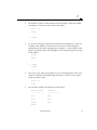
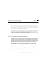
Feature Comparison of microSPARC-II and microSPARC-IIep . . . . . . . . . . . . . . . . . . 1
Big Endian Example . . . . . . . . . . . . . . . . . . . . . . . . . . . . . . . . . . . . . . . . . . . . . . . . . . . 7
Little Endian Example . . . . . . . . . . . . . . . . . . . . . . . . . . . . . . . . . . . . . . . . . . . . . . . . . . 8
microSPARC-II CPU Performance Summary . . . . . . . . . . . . . . . . . . . . . . . . . . . . . . . 11
Benchmark Test Setup . . . . . . . . . . . . . . . . . . . . . . . . . . . . . . . . . . . . . . . . . . . . . . . . . 12
Test Results for SPECint92 . . . . . . . . . . . . . . . . . . . . . . . . . . . . . . . . . . . . . . . . . . . . . 12
Test Results for SPECfp92. . . . . . . . . . . . . . . . . . . . . . . . . . . . . . . . . . . . . . . . . . . . . . 13
Cycles for a Branch . . . . . . . . . . . . . . . . . . . . . . . . . . . . . . . . . . . . . . . . . . . . . . . . . . . 14
Instructions Taking Multiple Cycles . . . . . . . . . . . . . . . . . . . . . . . . . . . . . . . . . . . . . . 16
Cycles per Instruction . . . . . . . . . . . . . . . . . . . . . . . . . . . . . . . . . . . . . . . . . . . . . . . . . 28
Floating-Point State Register (FSR) Summary . . . . . . . . . . . . . . . . . . . . . . . . . . . . . . 53
FPU Instruction Cycle Counts . . . . . . . . . . . . . . . . . . . . . . . . . . . . . . . . . . . . . . . . . . . 54
Address Map for MMU Registers . . . . . . . . . . . . . . . . . . . . . . . . . . . . . . . . . . . . . . . . 60
Parity Control Definition . . . . . . . . . . . . . . . . . . . . . . . . . . . . . . . . . . . . . . . . . . . . . . . 62
Store Allocate Setting . . . . . . . . . . . . . . . . . . . . . . . . . . . . . . . . . . . . . . . . . . . . . . . . . 63
SFSR Level Field . . . . . . . . . . . . . . . . . . . . . . . . . . . . . . . . . . . . . . . . . . . . . . . . . . . . . 66
SFSR Access Type Field . . . . . . . . . . . . . . . . . . . . . . . . . . . . . . . . . . . . . . . . . . . . . . . 66
SFSR Fault Type Field . . . . . . . . . . . . . . . . . . . . . . . . . . . . . . . . . . . . . . . . . . . . . . . . . 67
Setting of SFSR Fault Type Code . . . . . . . . . . . . . . . . . . . . . . . . . . . . . . . . . . . . . . . . 67
Priority of Fault Types on Single Access . . . . . . . . . . . . . . . . . . . . . . . . . . . . . . . . . . . 68
Overwrite Operations . . . . . . . . . . . . . . . . . . . . . . . . . . . . . . . . . . . . . . . . . . . . . . . . . . 69
PCI Speed Select . . . . . . . . . . . . . . . . . . . . . . . . . . . . . . . . . . . . . . . . . . . . . . . . . . . . . 70
TLB Entry Address Mapping. . . . . . . . . . . . . . . . . . . . . . . . . . . . . . . . . . . . . . . . . . . . 76
microSPARC-IIep User’s Manual — April 1997
Table 5-12
Table 5-13
Table 5-14
Table 5-15
Table 5-16
Table 5-17
Table 5-18
Table 5-19
Table 5-20
Table 5-21
Table 5-22
Table 5-23
Table 5-24
Table 5-25
Table 5-26
Table 6-1
Table 6-2
Table 7-1
Table 7-2
Table 8-1
Table 8-2
Table 8-3
Table 8-4
Table 8-5
Table 9-1
Table 9-2
Table 9-3
Table 9-4
Table 9-5
Table 9-6
Table 9-7
Table 9-8
Table 9-9
Table 9-10
Table 9-11
Table 9-12
xvi
Page Table Entry Level in TLB . . . . . . . . . . . . . . . . . . . . . . . . . . . . . . . . . . . . . . . . . . 77
Page Table Access Permission . . . . . . . . . . . . . . . . . . . . . . . . . . . . . . . . . . . . . . . . . . . 78
Size of Page Tables . . . . . . . . . . . . . . . . . . . . . . . . . . . . . . . . . . . . . . . . . . . . . . . . . . . 79
Virtual Tag Match Criteria . . . . . . . . . . . . . . . . . . . . . . . . . . . . . . . . . . . . . . . . . . . . . . 80
TLB Entry Flushing . . . . . . . . . . . . . . . . . . . . . . . . . . . . . . . . . . . . . . . . . . . . . . . . . . . 82
Return Value for MMU Probes . . . . . . . . . . . . . . . . . . . . . . . . . . . . . . . . . . . . . . . . . . 83
MISC MMU, and Performance Counter Control Space . . . . . . . . . . . . . . . . . . . . . . . 84
Memory Request Type . . . . . . . . . . . . . . . . . . . . . . . . . . . . . . . . . . . . . . . . . . . . . . . . . 87
MMU Breakpoint Register MT Field Decode . . . . . . . . . . . . . . . . . . . . . . . . . . . . . . . 92
MMU Breakpoint Register TWS Field Decode. . . . . . . . . . . . . . . . . . . . . . . . . . . . . . 93
MMU Breakpoint Register VAM Field Decode . . . . . . . . . . . . . . . . . . . . . . . . . . . . . 93
MMU Breakpoint Register VAS Field Decode . . . . . . . . . . . . . . . . . . . . . . . . . . . . . . 93
Mask ID . . . . . . . . . . . . . . . . . . . . . . . . . . . . . . . . . . . . . . . . . . . . . . . . . . . . . . . . . . . . 95
TLB Reference Priority . . . . . . . . . . . . . . . . . . . . . . . . . . . . . . . . . . . . . . . . . . . . . . . . 96
Translation Modes . . . . . . . . . . . . . . . . . . . . . . . . . . . . . . . . . . . . . . . . . . . . . . . . . . . . 97
Data Cache Fill Ordering . . . . . . . . . . . . . . . . . . . . . . . . . . . . . . . . . . . . . . . . . . . . . . 103
Flush Criteria for ASI 0x10-0x14 . . . . . . . . . . . . . . . . . . . . . . . . . . . . . . . . . . . . . . . 104
Instruction Cache Fill Ordering . . . . . . . . . . . . . . . . . . . . . . . . . . . . . . . . . . . . . . . . . 110
Flush Criteria for ASI 0x10-0x14 . . . . . . . . . . . . . . . . . . . . . . . . . . . . . . . . . . . . . . . 112
Memory Bank Population . . . . . . . . . . . . . . . . . . . . . . . . . . . . . . . . . . . . . . . . . . . . . 114
Physical Address Decode for System Memory . . . . . . . . . . . . . . . . . . . . . . . . . . . . . 117
Refresh Rate Control Bits . . . . . . . . . . . . . . . . . . . . . . . . . . . . . . . . . . . . . . . . . . . . . 119
Processor Core Clock Speeds Available . . . . . . . . . . . . . . . . . . . . . . . . . . . . . . . . . . 120
Number of Cycles for Different Interfaces . . . . . . . . . . . . . . . . . . . . . . . . . . . . . . . . 121
PCI Controller Fixed Memory Map (0x3000.0000 to 0x30ff.ffff). . . . . . . . . . . . . . . 129
Basic PCI Bus Operations and Restrictions . . . . . . . . . . . . . . . . . . . . . . . . . . . . . . . . 134
PCI Bus Commands . . . . . . . . . . . . . . . . . . . . . . . . . . . . . . . . . . . . . . . . . . . . . . . . . . 136
Configuration/Control Register Addresses . . . . . . . . . . . . . . . . . . . . . . . . . . . . . . . . 138
PCI Vendor ID Register (4 bytes @ offset = 00) . . . . . . . . . . . . . . . . . . . . . . . . . . . . 140
PCI Revision Register (1 byte @ offset = 08) . . . . . . . . . . . . . . . . . . . . . . . . . . . . . . 140
PCI Class Code Register (3 bytes @ offset = 09) . . . . . . . . . . . . . . . . . . . . . . . . . . . 140
PCI Header Type Register (1 byte @ offset = 0E). . . . . . . . . . . . . . . . . . . . . . . . . . . 140
PCI Command Register (2 bytes @ offset = 04) . . . . . . . . . . . . . . . . . . . . . . . . . . . . 141
PCI Status Register (2 bytes @ offset = 06) . . . . . . . . . . . . . . . . . . . . . . . . . . . . . . . 142
PCI Cache Line-Size Register (1 byte @ offset = 0D) . . . . . . . . . . . . . . . . . . . . . . . 143
PCI Latency Timer Register (1 byte @ offset = 0C) . . . . . . . . . . . . . . . . . . . . . . . . . 143
microSPARC-IIep User’s Manual — April 1997
Table 9-13
Table 9-14
Table 9-15
Table 9-16
Table 9-17
Table 9-18
Table 9-19
Table 9-20
Table 9-21
Table 9-22
Table 9-23
Table 9-24
Table 9-25
Table 9-26
Table 9-27
Table 9-28
Table 9-29
Table 9-30
Table 9-31
Table 9-32
Table 9-33
Table 9-34
Table 9-35
Table 9-36
Table 9-37
Table 9-38
Table 9-39
Table 9-40
Table 9-41
Table 9-42
Table 9-43
Table 9-44
Table 9-45
Table 9-46
Table 9-47
Table 9-48
PCI BIST Register (1 byte @ offset = 0F). . . . . . . . . . . . . . . . . . . . . . . . . . . . . . . . .
PCI Counters (4 bytes @ offset = 40) . . . . . . . . . . . . . . . . . . . . . . . . . . . . . . . . . . . .
PCI Discard Counter (2 bytes @ offset = 68) . . . . . . . . . . . . . . . . . . . . . . . . . . . . . .
System Memory Base Address Register 0 (SMBAR0) (1 byte @ offset = A0) . . . .
System Memory Size Register 0 (MSIZE0) (1 byte @ offset = A1) . . . . . . . . . . . . .
PCI Memory Base Address Register 0 (PMBAR0) (1 byte @ offset = A2) . . . . . . .
System Memory Base Address Register 1 (SMBAR1) (1 byte @ offset = A4) . . . .
System Memory Size Register 1 (MSIZE1) (1 byte @ offset = A5) . . . . . . . . . . . . .
PCI Memory Base Address Register 1 (PMBAR1) (1 byte @ offset = A6) . . . . . . .
System I/O Base Address Register (SIBAR) (1 byte @ offset = A8) . . . . . . . . . . . .
System I/O Size Register (ISIZE) (1 byte @ offset = A9). . . . . . . . . . . . . . . . . . . . .
PCI I/O Base Address Register (PIBAR) (1 byte @ offset = AA) . . . . . . . . . . . . . .
PCI Base Address Register (PCIBASE0) (4 bytes @ offset = 10,14,18,1C,20,24). .
PCI Memory Size Register (PCISIZE0) (4 bytes @ offset = 44,48,4C,50,54,58) . .
PCI IOTLB Control Register (PCICR) (1 byte @ offset = 84) . . . . . . . . . . . . . . . . .
PCI IOTLB RAM Input Register (PCIRIR) (4 bytes @ offset = 90) . . . . . . . . . . . .
PCI IOTLB CAM Input Register (PCICIR) (4 bytes @ offset = 94) . . . . . . . . . . . .
PCI IOTLB RAM Output Register (PCIROR) (4 bytes @ offset = 98) . . . . . . . . . .
PCI IOTLB CAM Output Register (PCICOR) (4 bytes @ offset = 9C) . . . . . . . . . .
PCIC IOTLB Translation Error Address Register (4 bytes @offset = CC). . . . . . . .
PCIC PIO Error Command Register (1 byte @offset = C7) . . . . . . . . . . . . . . . . . . .
PCIC PIO Error Address Register (4 byte @offset = C8) . . . . . . . . . . . . . . . . . . . . .
PCIC Arbitration Assignment Select Register (2 bytes @ offset = 8A) . . . . . . . . . .
PCIC PIO Control Register (1 byte @ offset = 60) . . . . . . . . . . . . . . . . . . . . . . . . . .
PCIC DVMA Control Register (1 byte @ offset = 62) . . . . . . . . . . . . . . . . . . . . . . .
PCIC Arbitration/Interrupt Control Register (1 byte @ offset = 63) . . . . . . . . . . . . .
PCIC Interrupt Assignment Select Register (2 bytes @ offset = 88). . . . . . . . . . . . .
PCIC Interrupt Assignment Select Register (2 bytes @ offset = 8C) . . . . . . . . . . . .
PCIC System Interrupt Pending Register (4 bytes @ offset = 70). . . . . . . . . . . . . . .
PCIC Clear System Interrupt Pending Register (1 byte @ offset = 83) . . . . . . . . . .
PCIC System Interrupt Target Mask Register (4 bytes @ offset = 74) . . . . . . . . . . .
PCIC System Interrupt Target Mask Clear Register (4 bytes @ offset = 78) . . . . . .
PCIC System Interrupt Target Mask Set Register (4 bytes @ offset = 7C) . . . . . . . .
PCIC Processor Interrupt Pending Register (4 bytes @ offset = 64). . . . . . . . . . . . .
PCIC Default (Reset) Interrupt Assignments. . . . . . . . . . . . . . . . . . . . . . . . . . . . . . .
PCIC Software Interrupt Clear Register (2 bytes @ offset = 6A) . . . . . . . . . . . . . . .
List of Tables
143
143
144
145
145
145
146
146
147
147
148
148
149
151
154
155
156
157
158
158
159
159
160
162
164
165
167
167
169
171
172
172
173
173
174
175
xvii
Table 9-49
Table 9-50
Table 9-51
Table 9-52
Table 9-53
Table 9-54
Table 9-55
Table 9-56
Table 9-57
Table 9-58
Table 9-59
Table 9-60
Table 9-61
Table 9-62
Table 9-63
Table 10-1
Table 11-1
Table 11-2
Table 11-3
Table 12-1
Table A-1
Table B-1
xviii
PCIC Software Interrupt Set Register (2 bytes @ offset = 6E) . . . . . . . . . . . . . . . . . 175
PCIC Software Interrupt Output Register (2 bytes @ offset = 8E) . . . . . . . . . . . . . . 176
PCIC Counter-Timers Address Map . . . . . . . . . . . . . . . . . . . . . . . . . . . . . . . . . . . . . 178
Processor Counter Limit or User Timer MSW (Word only @ offset = AC) . . . . . . . 178
User Timer Read/Write Sequence Required . . . . . . . . . . . . . . . . . . . . . . . . . . . . . . . 179
Processor Counter or User Timer LSW (Word Only @ offset = B0) . . . . . . . . . . . . 179
Processor Counter Limit Pseudo Register (Word Only @ offset = B4) . . . . . . . . . . 180
System Counter Limit Register (Word Only @ offset = B8). . . . . . . . . . . . . . . . . . . 180
System Counter Register (Word Only @ offset = BC) . . . . . . . . . . . . . . . . . . . . . . . 180
System Counter Limit or User Timer MSW (Word Only @ offset = C0) . . . . . . . . . 181
User Timer Start/Stop Register (1 byte @ offset = C4) . . . . . . . . . . . . . . . . . . . . . . . 181
Processor Counter/User Timer Configuration Register (1 byte @ offset = C5) . . . . 182
Counter Interrupt Priority Assignment Register (1 byte @ offset = C6) . . . . . . . . . . 182
System Status and Control Register (1 byte @ offset = D0) . . . . . . . . . . . . . . . . . . . 183
PCI Control Space Registers . . . . . . . . . . . . . . . . . . . . . . . . . . . . . . . . . . . . . . . . . . . 185
Flash ROM Interface Support . . . . . . . . . . . . . . . . . . . . . . . . . . . . . . . . . . . . . . . . . . 188
Internal Clock Divide Control . . . . . . . . . . . . . . . . . . . . . . . . . . . . . . . . . . . . . . . . . . 196
JTAG Instructions. . . . . . . . . . . . . . . . . . . . . . . . . . . . . . . . . . . . . . . . . . . . . . . . . . . . 206
Boot Mode Select (BM_SEL) . . . . . . . . . . . . . . . . . . . . . . . . . . . . . . . . . . . . . . . . . . 213
Error Summary. . . . . . . . . . . . . . . . . . . . . . . . . . . . . . . . . . . . . . . . . . . . . . . . . . . . . . 215
ASI’s Supported by microSPARC-IIep . . . . . . . . . . . . . . . . . . . . . . . . . . . . . . . . . . . .218
Physical Address Space . . . . . . . . . . . . . . . . . . . . . . . . . . . . . . . . . . . . . . . . . . . . . . . .223
microSPARC-IIep User’s Manual — April 1997
Preface
The microSPARCTM-IIep is an extension of the SPARCTM processor family targeted for low-cost applications. The microSPARC-IIep RISC processor allows systems designers to take advantage of a highly integrated SPARC system on a chip
and achieve industry-leading performance.
The microSPARC-IIep integrates a 32-bit SPARC processor with floating-point
unit, memory management unit, separate instruction and data caches, PCI bus
controller, DRAM and flash memory controller, and clock generator using phaselocked loop on to a single device. Implemented with state-of-the-art CMOS technology, the microSPARC-IIep provides an ideal low-cost, high-performance, and
low-power-consumption solution.
Like all SPARC processors, microSPARC-IIep processors are supported by the industry’s largest installed base of native RISC development environments, applications, and support tools. SPARC is the leading microprocessor technology
supporting the information superhighway infrastructure in terms of hardware
and software. These tools and technology make SPARC ideal for your embedded
and networked computing applications.
microSPARC-IIep Version
Refer to the contents of the device ID register (see Figure 11-4 on page 205) for the
version of the microSPARC-IIep covered by this manual.
microSPARC-IIep User’s Manual — April 1997
xix
References
xx
1.
The SPARC Architecture Manual, Version 8, of December 11, 1990.
2.
PCI Local Bus Specification, Revision 2.1 June 1, 1995.
3.
microSPARC Microprocessor User’s Manual, STP1010TAB50, Rev. 1.0, June
1994.
4.
microSPARC-II Microprocessor User’s Guide, STP1012PGA-UG, Rev 1.1, July
1994.
5.
microSPARC-II Microprocessor User’s Guide Errata, STP1012-UGE.
6.
microSPARC-IIep Highly Integrated 32-bit RISC/PCI Microprocessor Data Sheet,
802-7327-03, February, 1997.
7.
IEEE standard 1149.1, IEEE Standard Test Access Port and Boundary Scan
Architecture, IEEE, 1990.
microSPARC-IIep User’s Manual — April 1997
1
microSPARC-IIep Overview
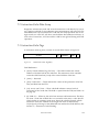
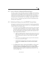
1.1 Introduction
The microSPARC-IIep CPU is a highly integrated, low-cost implementation of the
SPARC version 8 RISC architecture with a PCI interface. Its implementation
evolved from Sun’s microSPARC architecture.
•
High performance is achieved by the high level of integration, including onchip instruction and data caches, built-in DRAM controller, and PCI local bus
controller.
•
A full-custom implementation allows for a target frequency of 100-133MHz
providing sustained performance.
•
The design is highly testable with support of full JTAG scan.
•
The microSPARC-IIep chip supports up to 256MBytes of DRAM and 4
external PCI slots.
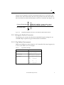
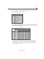
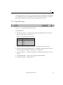
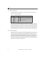
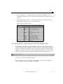
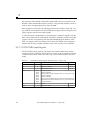
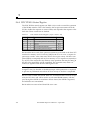
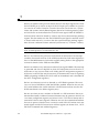
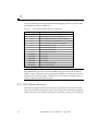
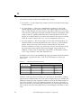
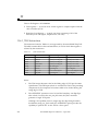
Table 1-1 lists the key differences between microSPARC-IIep and microSPARC-II.
Table 1-1
Feature Comparison of microSPARC-II and microSPARC-IIep
Feature
Overall
Frequency
microSPARC-II
microSPARC-IIep
•
32-bit SPARC Architecture version 8
•
Supports big-endian byte ordering
•
Supports little- and big-endian byte
ordering
•
110MHz
•
100MHz - 133MHz
microSPARC-IIep User’s Manual — April 1997
1
1
Table 1-1
Feature Comparison of microSPARC-II and microSPARC-IIep (Continued)
Feature
Integer Unit
Floating-Point Unit
Memory Management
Unit
Data Cache
microSPARC-II
microSPARC-IIep
•
136-word register file with 8 windows and 8 global registers
•
5-stage pipeline
•
Supports branch folding
•
4-deep instruction queue supporting instruction prefetching
•
Support instruction and data cache streaming
•
Support big-endian byte ordering
•
Supports all single- and double-precision floating-point SPARC version 8 instructions
•
Traps all quad-precision floating-point instructions
•
Datapath contains Meiko floating-point engine, fast multiply unit.
•
Support of simultaneous execution of fast multiplications and other floating-point
operations such as floating-point add.
•
3-entry floating-point deferred trap queue
•
32 floating-point registers of 32 bits wide
•
SPARC version 8 Reference MMU
•
Translates 32-bit virtual address to 31-bit physical address
•
Supports 8 different 256MByte address spaces
•
Supports 256 contexts
•
64-entry fully-associative TLB with
pseudo random replacement algorithm
•
32-entry fully-associative TLB with
pseudo random replacement algorithm
•
Unified memory TLB and IO TLB
•
Separate memory TLB and IO TLB
•
Supports hardware table-walks
•
8KByte, direct-mapped, virtually-indexed, virtually-tagged, write-through with
write-allocate
•
512 lines of 16 bytes
•
Support little- and big-endian byte
ordering
•
4-deep write buffer of 64 bits wide
Instruction Cache
•
16KByte, direct-mapped, virtually-indexed, virtually-tagged
•
512 lines of 32 bytes
Graphics Bus Interface
•
High-speed local bus
2
•
Not supported
microSPARC-IIep User’s Manual — April 1997
1
Table 1-1
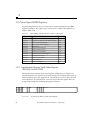
Feature Comparison of microSPARC-II and microSPARC-IIep (Continued)
Feature
Memory Interface
Local Bus Controller
Flash Memory Interface
microSPARC-II
microSPARC-IIep
•
Programmable DRAM controller
•
Supports up to 256MBytes of system memory
•
64-bit data and 2-bit parity
•
8 RAS lines
•
4 CAS lines
•
Supports 2 pages at a time
•
Supports 5V/3V standard/slow refresh, self-refresh
•
Supports fast-page mode DRAM only
•
Supports FPM or EDO DRAM that
meets fast-page mode timing
•
SBus
•
PCI revision 2.1
•
32-bit, 33MHz
•
Supports up to 4 external bus masters
or slaves
•
Supports host and satellite modes.
•
Address translation from 32-bit local
bus address to main memory space
assisted by dedicated 16-entry IO TLB
•
Supports little- and big-endian byte
ordering
•
Interrupt controller with programmable priority assignments and programmable output pins
•
Programmable local bus to chip frequency
•
Supports 8-bit or 32-bit interface
•
Pin-selectable boot choice
•
Not supported
Boundary Scan JTAG
TAP Controller
Packaging
•
321 pins pin grid array
Performance
Voltage
•
272 pins plastic ball grid array
•
72 SPECint92
•
59 SPECfp92
•
208K Dhrystone
•
Core operating voltage of 3.3V
1.2 microSPARC-IIep Memory Map
The microSPARC-IIep physical memory address mapping is shown in
Appendix B, Physical Memory Address Map.
microSPARC-IIep Overview
3
1
1.3 Endian Support
The microSPARC-II works only with big endian data. The microSPARC-IIep
works with either big endian or little endian data. To do so, the microSPARC-IIep
has built-in endian conversion logic. When operating on little endian data, the
endian conversion logic performs byte swapping to convert external little endian
data to internal big endian data and internal big endian data to external little endian data. The endian conversion logic is enabled by bits 15 and 16 of the processor state register (PSR) and bit 2 of the PCI controller PIO control register.
1.3.1 Processor-to-System Memory Endian Conversion
The microSPARC-IIep supports little endian system memory data for both supervisory and user modes. PSR bits 16 and 15 enable little endian conversion during
supervisor and user modes, respectively:
•
PSR [16]: When set, the default byte ordering for supervisor data references is
little endian. When clear, the default byte ordering for supervisor data
references is big endian.
•
PSR[15]: When set, the default byte ordering for user data references is little
endian. When clear, the default byte ordering for user data references is big
endian.
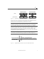
For example (see Figure 1-1):
4
•
Processor operating little endian mode: If the contents of a double word
register (r2,r3) = 0001.0203.0405.0607 and a double word store to memory
location 0 is issued, the double word at memory location 0 would contain
0706.0504.0302.0100 after the transfer.
•
Processor operating in big endian mode: If the same double word register was
transferred to memory location 0 while operating in big endian mode, the
double word at memory location 0 would contain 0001.0203.0405.0607 after
the transfer.
microSPARC-IIep User’s Manual — April 1997
1
Big Endian Mode
Little Endian Mode
(r2,r3)
00010203 04050607
00010203 04050607
(mem0,mem1)
00010203 04050607
07060504 03020100
Figure 1-1
Big Endian vs. Little Endian Example (Processor Double Word Store)
All loads and stores, including ones using address space identifiers (ASI), are
handled in the mode designated by the PSR endian control bit.
Note: Please remember to check the PSR endian control bits while performing
maintenance operations in little endian mode. Failure to do so may result in
erroneous failure indications because the data may appear to be scrambled.
Switching of endian modes does not take effect until after completion of the instruction immediately following the PSR endian control bits update. When
switching between endian modes, the instruction following the PSR modification
will operate in the previous endian mode.
Note: When switching modes, the software must include a NOP, non-memory,
or ASI shadow instruction following an update to the PSR (see Figure 1-2).
Previous Endian Mode
New Endian Mode
Figure 1-2
...
instr
LOAD PSR /* change endian mode */
NOP/non-memory/ASI instruction /* required */
instr
instr
...
Required Shadow Instruction at Processor Endian Mode Switch
microSPARC-IIep Overview
5
1
Caching of data is allowed while operating in little endian mode, but there is no
hardware mechanism in the data cache to determine if a particular datum is
stored in big or little endian format. The endian mode of the cached data is determined by the context identity value of the process. By tracking the context identity, the user can determine the endian mode of the cached data.
Note: Certain hardware operations of the microSPARC-IIep processor assume
the byte ordering of the data references to be big endian only. For example,
independent of the PSR settings, the data references for table walks are treated as
big endian data.
There is no performance penalty while operating in little endian mode.
1.3.2 Processor-to-PCI Endian Conversion
The endian conversion logic across the processor-to-PCI interface is controlled by
bit 2 of the PCI controller PIO control register (PA=0x300C.0060). On reset, the endian conversion logic is enabled. Therefore, data on the PCI bus is little endian.
For example (see Figure 1-3):
•
If the processor is operating in big endian mode, has contents
0001.0203.0405.0607 in the double word register (r2,r3), and bit 2 is set to 0,
then a PIO initiated PCI memory write would place the data 0302.0100 then
0706.0504 on the PCI bus in consecutive transactions.
•
With bit 2 set to 1, no twisting is done. If the processor is operating in big
endian mode with bit 2 set and has contents 0001.0203.0405.0607 in the double
word register (R2,R3), then a PIO initiated PCI memory write would place the
data 0001.0203 then 0405.0607 on the PCI bus in consecutive transactions.
Big Endian Mode
Little Endian Mode
(r2,r3)
00010203 04050607
00010203 04050607
(PCI Bus)
00010203 04050607
03020100 07060504
Figure 1-3
6
Big Endian vs. Little Endian Example (PCI Master Double Word Transfer)
microSPARC-IIep User’s Manual — April 1997
1
This bit can be changed on the fly. The preferred method is to set the bit to the
desired value, then read back the bit. This will guarantee that other PIO transactions are locked out while the PIO endian control is in transition (see Figure 1-4).
Previous Endian Mode
New Endian Mode
Figure 1-4
...
instr
LOAD PCIC CONFIG /* change endian mode */
READ PCIC CONFIG instruction /* required */
instr
instr
...
Required Readback Instruction at PCI Master Endian Mode Switch
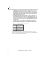
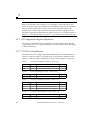
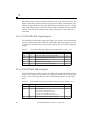
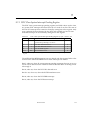
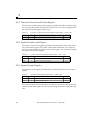
1.3.3 Settings for Endian Conversion
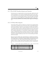
The following two sections describe the recommended register settings for microSPARC-IIep to operate in big and little endian environments.
1.3.3.1 Big Endian Environment
PSR[16] and PSR[15] are both cleared to 0. PCI controller PIO control register [2]
is set to 1. See Table 1-3 for an example.
Table 1-2
Big Endian Example
Location
Data
microSPARC-IIep register
r2
r3
00010203 04050607
System memory
addr 0
7
data 00010203 04050607
PCI local bus
AD
CBE
data
31
0
3
0
00010203
AD
CBE
data
31
0
3
0
04050607
microSPARC-IIep Overview
7
1
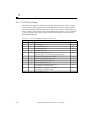
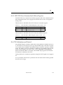
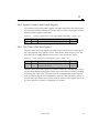
1.3.3.2 Little Endian Environment
PSR[16] and PSR[15] are set to 1 depending on whether data access is in supervisor or user mode. PCI controller PIO control register [2] is set to 0. See Table 1-3
for an example.
Table 1-3
Little Endian Example
Location
Data
microSPARC-IIep register
r2
r3
00010203 04050607
System memory
addr 7
0
data 00010203 04050607
PCI local bus
AD
CBE
data
31
0
3
0
03020100
AD
CBE
data
31
0
3
0
07060504
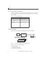
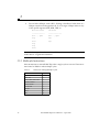
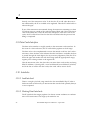
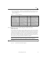
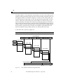
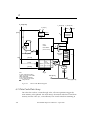
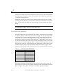
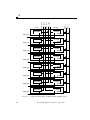
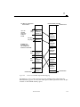
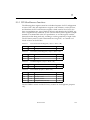
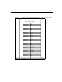
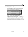
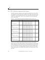
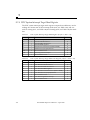
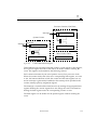
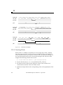
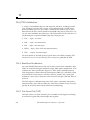
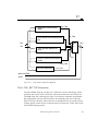
1.4 Block Diagram
Figure 1-5 shows the typical microSPARC-IIep system block diagram.
Flash
Memory
PCI Bus
microSPARC-IIep
Up to 4
PCI Bus
loads
Local Bus
32 MB DRAM SIMM Module
32 MB DRAM SIMM Module
32 MB DRAM SIMM Module
32 MB DRAM SIMM Module
Figure 1-5
Up to
256 MB
DRAM
SIMMs
Typical microSPARC-IIep System Block Diagram
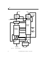
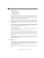
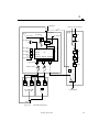
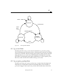
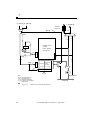
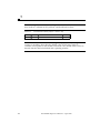
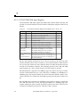
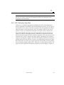
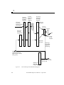
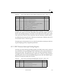
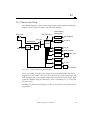
Figure 1-6 shows the microSPARC-IIep:
•
•
•
8
Integer unit (IU)
Floating-point unit (FPU)
Instruction and data caches
microSPARC-IIep User’s Manual — April 1997
1
•
Memory management unit (MMU) with 32-entry translation lookaside buffer
(TLB)
•
•
•
•
•
•
•
•
•
•
DRAM controller
PCI controller
PCI bus interface
IOMMU with 16-entry IOTLB
Flash memory interface
Interrupt controller
2 timers
Internal and boundary scan JTAG interface
Power management
Clock generation
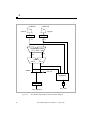
Figure 1-7 shows the microSPARC-IIep pipeline.
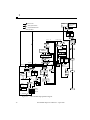
inst [31:0]
Integer Unit
PLL Clock
Generator
dpc [31:2]
Floating Point Unit
fp_dout [63:0]
d_va [31:0]
i_va [31:0]
64
instr
iu_dout [63:0]
Flash Memory
Interface
Instruction Cache
Data Cache
16K
8K
Write Buffer
4 Entry
Memory
Management Unit
32 Entry TLB
64-Bit Cache Fill Bus
Misc_bus [31:0]
Phy_addr [27:0]
Memory Interface
PCI Controller
Memory Data Bus <63:0>
Memory Address [11:0]
32-Bit PCI Bus
16-entry IOTLB
Addr
Figure 1-6
microSPARC-IIep Block Diagram
microSPARC-IIep Overview
9
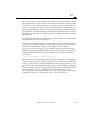
1
I/D VA<31:0>
PCQ
epc
Cache_fill bus<63:0>
branch folding
logic Pc
Physical Address<27:0>
Cache_fill<63:0>
ld_iu
iva
32
va
data
tag
I$ 16K
ld_fpu_w 64
prefetch
queue x4
32
fsr
R
R
bypass mux
alignment
bypass/signext mux
E
iu_dout
Cache_fill
64
E
E
dva
DIR
fpu regfile
32*32
IU regfile
8 windows
alu/sh
Meiko multiplier
fp
fpp
EIR
64
64
sb_ioa
fp_dout_e
va mux
TLB
wr buf x4
phy
32
entry add
cam sram
MEMIF
va
data
tag
D$ 8k
W
WIR
fpq
3 entry
32 bit PCI
b_memdata
MEMIF
PCIC
32 IOTLB
mm_pa 30
Misc_bus 32
par
Herbulator &
64b aligner
dpar
ipar
64
DRAM
3 cycle
access
b_memdata 64
Figure 1-7
10
microSPARC-IIep Pipeline Diagram
microSPARC-IIep User’s Manual — April 1997
RIR
2
CPU Performance
The performance projections for the microSPARC-IIep CPU is extrapolated from
the actual performance figures for the microSPARC-II. This is possible because
the microSPARC-IIep CPU is based on the design of the microSPARC-II core.
There are, however, minor differences in the I/O subsystem and the translation
lookaside buffer (TLB) of the microSPARC-II and microSPARC-IIep (i.e., the microSPARC-II CPU has a 64-entry TLB with 16 entries dedicated for IOTLB use,
while the microSPARC-IIep CPU has a 32-entry TLB). As a result, adjustments
have to be made to the microSPARC-II data to account for these differences.
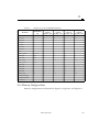
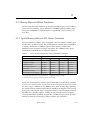
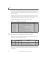
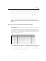
2.1 Benchmark Test Results
The results of these benchmark tests at 100MHz on microSPARC-II machines is
presented in Table 2-1.
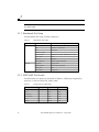
Table 2-1
microSPARC-II CPU Performance Summary
Benchmark
100MHz
SPECint92
72.29
SPECfp92
59.28
Dhrystone
208.33K
MIPS
118.57
MFLOPS
8.89
microSPARC-IIep’s SPECint92 is anticipated to drop in performance by 4.5% and
its SPECfp92 by 0.9% from these microSPARC-II results.
microSPARC-IIep User’s Manual — April 1997
11
2
Note: Performance of programs that overflow the available TLB entries will be
less than listed.
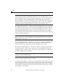
2.1.1 Benchmark Test Setup
The benchmark test setup is listed in Table 2-2.
Table 2-2
Benchmark Test Setup
Item
Hardware
Software
Configuration
Model Number
SPARCstation 5-100
CPU
100MHz microSPARC II
FPU
Integrated
Number of CPUs
1
Primary Cache
16KByte instruction + 8KByte data on chip
Other Cache
None
Memory
64MByte
Disk Subsystem
1GByte single-ended SCSI
Compilers
Apogee 3.051
Other Software
Kuck & Associates KAP
File System
UFS
System State
Single User
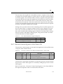
2.1.2 SPECint92 Test Results
The SPECint92 test results are presented in Table 2-3. SPECint92 computed by
best runs is 72.29 and SPECrate_int92 is 1864.
Table 2-3
Test Results for SPECint92
Benchmark
12
Copies
Elapsed Time
Best Runs
008.espresso
1
35.70
70.28
022.li
1
87.00
75.82
023.eqntott
1
7.80
154.93
026.compress
1
70.80
41.22
072.sc
1
36.80
135.22
085.gcc
1
117.90
51.12
microSPARC-IIep User’s Manual — April 1997
2
2.1.3 SPECfp92 Test Results
The SPECfp92 test results are presented in Table 2-4. SPECfp92 computed by best
runs is 59.28.
Table 2-4
Test Results for SPECfp92
Benchmark
Copies
lapsed Time
Best Runs
013.spice2g6
1
542.90
44.21
015.doduc
1
37.10
50.13
034.mdljdp2
1
97.70
72.57
039.wave5
1
99.50
37.19
047.tomcatv
1
44.80
59.15
048.ora
1
79.30
93.57
052.alvinn
1
68.20
112.76
056.ear
1
285.00
89.47
077.mdljsp2
1
81.40
41.15
078.swm256
1
311.90
40.72
089.su2cor
1
207.40
62.20
090.hydro2d
1
298.00
45.97
093.nasa7
1
245.80
68.35
094.fpppp
1
152.20
60.45
2.1.4 Dhrystone Test Results
This machine benchmarks at 208,333 Dhrystone/second.
2.2 Compiler Optimization Guidelines
This section explains some of the code scheduling issues that affect the performance of the microSPARC-IIep processor.
2.2.1 Branches
Integer branches are either folded with their delay slot instructions or allowed to
enter the integer pipeline.
Branch folding is supported by a four-deep instruction queue. The queue is filled
each cycle by a double word fetch. For a branch to be folded, the branch, delay
slot, and delay slot+1 instructions must be in the queue or is streaming to the in-
CPU Performance
13
2
teger unit (IU) from the instruction cache. In addition, the instruction preceding
the branch cannot be a multi-cycle instruction or a control transfer instruction
(CTI), and there cannot be a WRspec (write to a special register) in the pipe.
All branches are predicted taken. The target instruction is fetched in the D-stage
of the delay slot instruction (or branch-delay slot pair).
bicc 1f
delay
delay+1
...
1: target
...
Table 2-5 summarizes the cycles taken for a branch.
Table 2-5
Cycles for a Branch
Branch
Taken
Not Taken
Folded
0
1
Not Folded
1
1 or 2
If the branch can be folded, the branch and delay slot will be executed at cycle x.
If the branch is taken, the target will execute at cycle x+1. If the branch is not taken, the target must be killed and delay+1 will be executed at cycle x+2. Thus,
folded taken branches take 0 cycles, while folded untaken branches take 1 cycle.
If the branch cannot be folded, it enters into the pipeline at cycle x, and the delay
slot instruction enters at cycle x+1. If the branch was taken, the target will execute
at cycle x+2. If the branch was not taken, but the delay instruction+1 was in the
instruction queue, it will execute at cycle x+3; otherwise it must be fetched and
will execute at cycle x+4.
2.2.2 Guidelines for Branch Folding
1.
14
Try to make as many BICC's taken as possible since microSPARC-IIep
always predicts taken and fetches the target. If the branch is untaken, it
will cost a cycle if it was folded, and may cost an additional cycle if it was
not folded.
microSPARC-IIep User’s Manual — April 1997
2
2.
Avoid BICC to BICC control transfers. The target BICC cannot be folded
since delay+1 will not be in the instruction queue.
bicc
1f
delay
...
1:
bicc2f
...
3.
Try to have CTI target instructions be double word aligned (e.g., label 1 is
a double word address). This allows the odd word to enter the queue
immediately. If the odd word happens to be a BICC, it can be folded. If the
target is an odd word, the following BICC will not enter the queue and will
not be folded.
bicc1f
delay
...
1:
target
bicc2f
...
4.
Do not put save/restore in the delay slot of an annulling BICC. If the save/
restore is annulled, microSPARC-IIep must take a cycle to fix the current
window pointer (CWP).
bicc,a 1f
save
5.
Do not follow multicycle instructions with a BICC.
Will not Fold
Can Fold
--------------
---------------
std
std
bicc
add
delay
bicc
delay
CPU Performance
15
2
6.
Do not follow WRspec with a BICC. Folding is disallowed when there is a
WRspec anywhere in the pipeline's D, E, or W stages. WRspec refers to any
of the special registers (PSR, WIM, TBR, Y).
Will not Fold
Can Fold
--------------
---------------
mov .., %psr
mov .., %psr
nop
nop
bicc
nop
nop
nop
bicc
Note: Only integer branches are folded. FP branches are not. Calls are not
folded due to a register file limitation.
2.2.3 Multicycle Instructions
Most instructions in microSPARC-IIep take a single cycle to execute. The instructions listed in Table 2-6 take multiple cycles.
Table 2-6
Instructions Taking Multiple Cycles
Instruction
16
Cycles
JMP, RETT
2
LDA, STA
2
LDD, LDDA, STD, STDA
2
LDSTB, LDSTBA
2
SWAP, SWAPA
2
STA FLUSH
3
IFLUSH
3
IMUL
19
IDIV
39
microSPARC-IIep User’s Manual — April 1997
2
2.2.4 Pipeline Interlocks
microSPARC-IIep has several pipeline interlocks that may be avoided with improved code scheduling. The following operations will result in interlocks:
1.
An integer load immediately followed by an instruction that uses the load
destination as a source operand.
2.
A CALL followed by an instruction that uses r[15] of the register file as a
source operand.
3.
A RD to a special register followed by a dependent operation.
4.
A folded SAVE/RESTORE that was annulled.
5.
An unfolded CTI branch which is not taken and the delay slot + 1
instruction is not in the instruction queue.
2.2.5 Other Guidelines
Usage of the IMUL instruction, instead of a kernel routine, is preferred due to
higher performance. However, the performance gain of the IDIV instruction over
a kernel routine is highly dependent on the operand types. Therefore, usage of
the IDIV instruction may not always provide higher performance than a kernel
routine.
2.2.6 Floating-Point Instructions
Scheduling of floating-point (FP) instructions can have a large impact on FP performance. The most important thing to consider when scheduling FP code is
making efficient use of the floating-point queue. The FP unit has a three-entry
floating-point queue and two independent functional units (multiplier and everything else).
microSPARC-IIep does not interlock for FP loads, including double-word loads,
followed by dependent FP operations. Since operands for floating-point operations are read in W-stage, the result from the previous floating-point load can be
bypassed to the floating-point units.
Refer to Section 4.5, “FP Performance Factors for more information about floating-point performance.
CPU Performance
17
2
2.2.6.1 FP Interlocks
1.
FP queue full - if an FPOP is in E-stage and the FP queue is full, the pipe
must be held until the first instruction in the queue completes.
2.
FP store waiting for data from FPOP in queue - held in E-stage.
3.
FP load writing register used by FPOP in queue - held in W-stage. This
applies whether the FPOP register is RS1, RS2, or RD.
4.
FPLD followed by FPST - single cycle interlock if the FP register (modulo
2) being loaded is the same as the FP register being stored (modulo 2).
5.
FPLDFSR/FPSTDFQ followed by any FPOP/FPMEMOP/FPCMP - single
cycle interlock.
6.
FPOP followed by FPLDFSR/FPSTDFQ - LDFSR or STFSR must wait for
FPOP to complete.
7.
FP branch in decode and FCCV (FP condition code valid) deasserted. The
IU pipe will interlock until FCCV is reasserted. FCCV is deasserted when
an FCMP is started and reasserted when the FCMP completes. The branch
is held in D-stage.
2.2.6.2 Functional Units
There are two functional units: the multiplier and the Meiko core, which handles
all other operations. The multiplier can start an operation every three cycles, but
operations dependent on the multiplier results must wait five cycles for the result
to be written. The initial multiply must also be in the first queue entry if the second multiply is to be started before the first results are written. The Meiko core is
not pipelined; when an operation completes, the data and functional unit are
both available. See Chapter 4, “Floating-Point Unit for details on instruction cycle
count.
2.2.6.3 FP Queue Details
The FP queue is three entries deep. It allows out-of-order issue, but forces in-order completion. Only one operation can be started per cycle, and only one operation may complete per cycle. An operation does not leave the queue until it has
written its results. The following examples demonstrate how dependencies affect
the pipeline.
18
microSPARC-IIep User’s Manual — April 1997
2
1.
2.
3.
4.
5.
Out-of-order issue, no dependencies - data written back in-order, issued
out of order because of functional unit availability.
Unit
Issued
Written
fmuld
%f0, %f2, %f4
Mult
x
x+5
fmuld
%f6, %f8, %f10
Mult
x+3
x+8
faddd
%f12, %f14, %f16
Adder
x+2
x+9
FADD throughput - dependencies have no effect, 5 cycles per operation,
due to a single functional unit.
Unit
Issued
Written
faddd
%f0, %f2, %f2
Adder
x
x+5
faddd
%f2, %f2, %f0
Adder
x+5
x+10
FMUL throughput - no dependency, 3 cycles per operation.
Unit
Issued
Written
fmuld
%f0, %f2, %f4
Mult
x
x+5
fmuld
%f6, %f8, %f10
Mult
x+3
x+8
FMUL throughput - with dependency, 5 cycles per operation.
Unit
Issued
Written
fmuld
%f0, %f2, %f2
Mult
x
x+5
fmuld
%f0, %f2, %f2
Mult
x+5
x+10
FMUL/FADD pair - no dependency, 5 cycles per pair. The second multiply
cannot enter the queue until the first add has completed, at which time the
second add is being started.
Unit
Issued
Written
faddd
%f0, %f2, %f4
Adder
x
x+5
fmuld
%f6, %f8, %f10
Mult
x+1
x+6
faddd
%f0, %f2, %f4
Adder
x+5
x+10
fmuld
%f6, %f8, %f10
Mult
x+6
x+11
CPU Performance
19
2
6.
7.
8.
20
FMUL/FADD pair - one dependency, 6 cycles per pair. It doesn't matter
which way the dependency goes.
Unit
Issued
Written
faddd
%f0, %f2, %f4
Adder
x
x+5
fmuld
%f4, %f6, %f8
Mult
x+5
x+10
faddd
%f0, %f2, %f4
Adder
x+6
x+11
fmuld
%f4, %f6, %f8
Mult
x+11
x+16
Unit
Issued
Written
fmuld
%f0, %f2, %f4
Mult
x
x+5
faddd
%f4, %f6, %f8
dder
x+5
x+11
fmuld
%f0, %f2, %f4
Mult
x+6
x+11
faddd
%f4, %f6, %f8
Adder
x+11
x+16
FMUL/FADD/FMUL - two dependencies, 10 cycles per pair.
Unit
Issued
Written
faddd
%f0, %f2, %f4
Adder
x
x+5
fmuld
%f4, %f6, %f0
Mult
x+5
x+10
faddd
%f0, %f2, %f4
Adder
x+10
x+15
fmuld
%f4, %f6, %f8
Mult
x+15
x+20
Longer instructions (divide, square root) - other instructions can enter the
pipeline, but none will complete out of order. The integer pipe will not be
held unless a fourth FPop tries to enter the queue. Note that the second
multiply cannot start until the first advances to the first queue entry.
Unit
Issued
Written
fdivd
%f0, %f2, %f4
Adder
x
x+35
fmuld
%f6, %f8, %f10
Mult
x+1
x+36
fmuld
%f12, %f14, %f16
Mult
x+36
x+41
microSPARC-IIep User’s Manual — April 1997
2
2.2.7 Loads and Stores
Load and store ordering was found to have a large impact on microSPARC-IIep’s
performance. The microSPARC-IIep has a 8 KByte write through with write allocate data cache. If all accesses hit the cache, the order of accesses makes little difference. The order of access can have a large effect on the latency of cache misses
though. The following guidelines may help improve performance:
1.
Group memory accesses by DRAM page — Cache misses require reads
from DRAM. The DRAM access is faster if it can be accessed in page mode.
Therefore, loads and stores to the same page should be grouped together.
One way to do this is to group accesses which use the same base register
together, since these are likely to be in the same page. For instance:
Poor order:
Good order:
ld
[%o0], %f3
ld
[%o0], %f3
ld
[%i5-12], %f4
ld
[%o0+8], %f5
ld
[%o0+8], %f5
ld
[%i5-12], %f4
ld
[%i5-8], %f2
ld
[%i5-8], %f2
See Section 2.3, “Using the Two Page-Hit Registers for further
improvement by effectively using the page-hit registers.
2.
Minimize write buffer full penalty — microSPARC-IIep has four write
buffers. At higher frequencies, the write buffers will take more cycles to
flush. So, use fewer store instructions if possible, and reduce clustering of
stores to allow the buffers a chance to empty. One technique is to maximize
the use of store double (std). A double word store occupies only one write
buffer entry and takes one memory access. Storing the two registers
separately would require two write buffer entries and two memory
accesses.
Since microSPARC-IIep has four write buffers, up to four stores can be
clustered together without stalling the pipe if the stores hit. However, all
issued stores must be written to memory before the next cache miss can be
processed. It is recommended that the number of instructions between the
stores and the next memory access be roughly proportional to the number
of stores, to allow time for the write buffer to empty.
3.
Minimize usage of STB and STH — Memory accesses have word write
enables, so these instructions are implemented as a read-modify-write
memory operation. This is slower than a normal store.
CPU Performance
21
2
2.2.8 General Techniques
The following things will help performance, but are not microSPARC-IIep specific optimizations.
1.
Decrease instruction count.
2.
Reduce integer load use interlock through better instruction scheduling.
3.
Reduce register window overflow/underflow.
4.
Reduce cache miss rates, especially store miss rates.
2.3 Using the Two Page-Hit Registers
You can improve microSPARC-IIep’s performance by using the two page-hit registers. See Section 5.3.1, “Processor Control Register (VA[12:8]=0x00) for information on how to enable page-mode operations.
Each time a virtual address (VA) is translated for a memory operation, the resulting physical address (PA) is compared to the PA of the previous memory operation stored in the page-hit registers. If the two PAs are within the same 4KByte
physical address space, the MMU signals that the current operation is a page hit.
This indicates to the memory interface logic that there is no need to toggle the
RAS lines to the memory, and the overall access is therefore much faster. Every
memory access puts its page address into the page hit register.
In microSPARC-IIep, there are two page-hit registers. This allows the saving of
two PAs for possible page hits. This also requires the memory interface to divide
its memory into two groups, one for each page-hit register. Each group has its
own RAS lines also. The actual banks of memory are setup so that every other
bank/SIMM belongs to a given page-hit register.
The two page-hit registers will especially help applications that alternate a large
number of accesses between text and data. If there were only a single page-hit
register, text and data accesses would thrash the page hit register and reduce its
effectiveness.
With the existing page allocation software, the first group of pages have to be entirely used or allocated before any of the second group of pages are used. This
means that the benefit of having two page-hit registers is not seen until that point
is reached. This also means that when an application is mapped, the banks will
be used serially, one bank after another.
22
microSPARC-IIep User’s Manual — April 1997
2
To maximize the benefit of the page-hit register scheme, the two registers have to
be used as much as possible. This means dividing all of the available pages into
two groups that correspond to the two page-hit registers. After this is done, a
number of allocation preferences can be used. One group can be used for text and
the other for data, or simply alternate between the two groups. In microSPARCIIep, the DRAM page size is 4KByte, so alternating will make available a total of
8KByte of fast-access memory at any given time.
The difference between page and non-page access in microSPARC-IIep is 4 cycles
for a page hit versus 11 cycles for non-page hit.
Note: When the microSPARC-IIep accesses main memory on behalf of the PCIC
for PCI DMA accesses, the page-hit registers are marked invalid prior to the
DMA access to prevent hitting in these registers incorrectly.
CPU Performance
23
2
24
microSPARC-IIep User’s Manual — April 1997
3
Integer Unit
The microSPARC-IIep integer unit (IU) implements SPARC integer instructions as
defined in SPARC Architecture Manual version 8. It is derived from the integer
unit of the microSPARC-II. This implementation balances the needs of high-performance and low-cost while maintaining software compatibility. The only differences between the microSPARC-II and microSPARC-IIep integer units are noted
in Section 3.13, “Compliance With SPARC Version 8 in this chapter.
3.1 Overview
The microSPARC-IIep integer unit is a CMOS implementation of the SPARC 32bit RISC architecture version 8. Important features include:
•
•
•
•
•
•
•
•
5-stage instruction pipeline
Branch folding
Instruction and data cache streaming support
Hardware implementation of IMUL and IDIV
136-register register file supporting 8 register windows
Interface to on-chip floating-point unit
4-deep instruction queue supporting instruction prefetching
Little and big endian byte ordering support
microSPARC-IIep User’s Manual — April 1997
25
3
From I$
To I$
To FPU
I$
addr gen
Inst
Queue
To FPU
IRegs
Pipeline
Control
To/From
MMU
Execute
Datapath
To/From
FPU
8 -window
register
file
From FPU
D$ data/adr
From D$
Figure 3-1
26
To D$
IU Block Diagram
microSPARC-IIep User’s Manual — April 1997
3
3.2 Instruction Pipeline
The microSPARC-IIep IU uses a double (1 branch, 1 other) instruction issue pipeline with 5 stages.
1.
F (Instruction Fetch): Instruction fetch occurs in this stage. Instructions
may be fetched either from the 4-instruction deep queue or directly from
the instruction cache. The instruction is valid at the end of this stage and is
registered inside the IU.
2.
D (Decode): This stage decodes the instruction and reads the necessary
operands. Operands may come from the register file or from internal data
bypasses. The register file has 3 independent read ports — two for operand
or address calculation, and one for store operand read in the E-stage. For
situations where the necessary operand is in the pipeline and has not been
written to the register file yet, internal bypasses are supplied to prevent
pipeline interlocks. In addition, addresses are computed for CALL and
Branch in this stage.
3.
E (Execute): This stage performs ALU, logical, and shift operations. For
memory operations (e.g., LD) and for JMPL/RETT, the address is
computed in this stage. Store operand read is done in this stage from
register file’s third read port and sent to the data cache.
4.
W (Write): This stage accesses the data cache. For cache reads, the data will
be valid by the end of this stage, at which point it is aligned as appropriate.
Store data read out in the E-stage is written to the data cache at this time.
5.
R (Result): This stage loads the result of any ALU, logical, shift, or cache
read operation into the register file.
Integer Unit
27
3
Table 3-1 lists the cycles per instruction.
Table 3-1
Cycles per Instruction
Instruction
CALL
Cycles
1
Single Loads
1
Jump/Rett
2
Double Loads
2
Single Stores
1
Double Stores
2
LDF/LDDF
1
STF/STDF
1
LDA/STA
2
LDDA/STDA
2
STA FLUSH
3
IFLUSH
3
Taken Trap
3
Atomic Load/Store
2
3.3 Memory Operations
3.3.1 Loads
All load operations take 1 cycle in the microSPARC-IIep IU except for LDD which
takes 2. For LD, LDB, and LDH, the pipeline does the following:
28
1.
D — Register operands are read from the register file or are bypassed from
instructions still in the pipe. An immediate operand is sign extended.
2.
E — Address operands are added to compute the memory address. This
address is presented to the cache in this stage.
3.
W — Address is registered in the cache and access is started. Data is
expected at the end of this stage. Any necessary alignment and sign
extension is done by the data cache prior to being registered by the IU.
4.
R — Data is registered in the IU and is written into the register file.
microSPARC-IIep User’s Manual — April 1997
3
In the event of a cache miss, the miss signal is given to the IU in the W stage. The
miss signal holds the pipeline. Once the miss data is available, the cache signals
the IU to release the pipeline. The IU also registers the miss data into the appropriate R-stage register and writes it into the register file. As the cache line is being
filled, the IU can accept additional data either from within the filling line or from
another line that exists in the data cache.
An integer LDD takes 2 cycles to complete because of the use of 32-bit datapaths.
The pipeline does the following:
1.
D — Register operands are read from the register file or are bypassed from
instructions still in the pipe. An immediate operand is sign extended.
2.
E — Address operands are added to compute the even memory address.
This address is presented to the data cache in this stage.
3.
W (E2) — The even memory address is registered in the cache and access is
started. This data is sent to the IU. At the same time, the odd address is
generated by the IU and sent to the cache.
4.
R (W2) — The even word is registered in the IU and written to the register
file. The odd word address is registered in the cache and its access is
started.
5.
R2 — The odd word is registered in the IU and written to the register file.
In the event of a cache miss, the miss signal is generated in the W-stage of the
LDD. The miss holds the pipeline. When the cache receives the miss data, the IU
control releases the pipeline, registers the even data into the R register, and writes
it to the register file. It picks up the odd data in the next stage. As the cache line
is being filled, the IU can accept additional data either from the filling line or
from another line that exists in the data cache.
Floating-point load-single and load-double instructions (LDF/LDDF) operate like
an integer load, except that the floating-point register file is loaded with the data
coming from the data cache. In the case of LDDF, the instruction is executed in
only one stage using the 64-bit datapath that exists between data cache and FPU.
Integer Unit
29
3
3.3.2 Stores
The microSPARC-IIep IU register file has three independent read ports. As a result, store operations take 1 cycle, except integer STD which takes 2. For integer
stores and floating point single stores, the IU duplicates the store data on both
words of the 64-bit bus from IU to data cache. For floating point store double, the
words are aligned correctly.
1.
D — Register operands are read from the register file or are bypassed from
instructions still in the pipe. An immediate operand is sign extended.
2.
E — The store virtual address is computed in the ALU. The store operand
is read from the third read port of the register file — this includes potential
bypassing of results and a store aligner. If it is a floating point store of any
size, operands are read from the floating-point file instead. Integer and
floating point store data are correctly selected and sent to the data cache.
3.
W — The store data is registered by the data cache and written.
4.
R — The store is complete.
For integer STD the pipeline does the following:
1.
D — Register operands are read from the register file or are bypassed from
instructions still in the pipe. An immediate operand is sign extended.
2.
E (D2) — The address operands are added to compute the even memory
address and sent to the data cache. This address will be registered within
the IU to provide the data cache with the odd address in the next stage. At
the same time, the even store data is read from the register file’s port 3 or
bypassed from instructions still in the pipe and is sent to the data cache.
3.
W (E2) — The odd address is sent to the data cache. Odd word is read
from register file or bypassed from instructions still in the pipe and is sent
to the data cache. Even word is written to data cache.
4.
R (W2) — The odd word is written to the data cache.
5.
R2 — The STD complete.
3.3.3 Atomic Operations
SWAP and LDSTUB each take two cycles to complete. The pipeline does the following on the SWAP instruction:
30
microSPARC-IIep User’s Manual — April 1997
3
1.
D — Register operands are read from the register file or are bypassed from
instructions still in the pipe. An immediate operand is sign extended.
2.
E (D2) — The address operands are added to compute the swap memory
address. This address is sent to the data cache to start the cache read
portion of the operation. The register to be swapped is read out in this
stage and sent to the data cache.
3.
W (E2) — The data cache returns the memory location accessed. The
register to be swapped is sent to the data cache again. (The store address is
not sent to the data cache again).
4.
R (W2) — The IU registers the read data and writes it to the register file.
5.
R2 — The SWAP complete.
The pipeline does the following on the LDSTUB instruction:
1.
D — Register operands are read from the register file or are bypassed from
instructions still in the pipe. An immediate operand is sign extended.
2.
E (D2) — The address operands are added to compute the LDST address.
This address is sent to the data cache to start the cache read portion of the
operation. 0xffff.ffff is sent to the data cache along with the appropriate
bytemarks for the store.
3.
W (E2) — The data cache returns the memory location accessed and it is
shifted appropriately and sent to the IU. 0xffff.ffff is sent to the data cache
again. (The store address is not sent to the data cache again.)
4.
R (W2) — The IU registers the read data and writes it to the register file.
5.
R2 — LDSTUB complete.
3.4 ALU/Shift Operations
Most ALU and shift operations take a single cycle to complete. The exceptions are
integer multiply and integer divide. On add, subtract, boolean, and shift operations, the pipeline does the following:
1.
D — Operands are read from the register file or bypassed from instructions
still in the pipe.
Integer Unit
31
3
2.
E — Appropriate operation is executed in ALU or shifter. There is a
selective inverter on the B input of the ALU to allow for subtracts and
certain Boolean operation (e.g. ANDN).
3.
W — Result of operation is forwarded to the next stage.
4.
R — Result is stored in the register file.
3.5 Integer Multiply
Integer multiply normally takes 22 cycles to complete, but may complete in 19 cycles if the 3 instructions preceding the multiply instruction do not write into the
integer register file. The algorithm implemented in the microSPARC-IIep IU is a
modified Booth’s (2-bit) multiply. The multiply process can be broken up into 4
distinct steps:
Initialization:
1 - 4 cycles
Booth’s iteration:
16 cycles
Correction (ala Booth):
1 cycle
Writeback:
1 cycle
The first cycle is used to set up the registers used in the multiply. The RS1 and
RS2 registers are initialized to the operands of the multiply. The W-stage result
register and the RS2 register are used as accumulators. At the completion of the
multiply, the W-stage register contains the most significant 32 bits of the result
and the RS2 register contains the least significant 32 bits of the result. The Wstage register contents are then written to the Y register and the RS2 contents to
the destination register in the register file.
3.6 Integer Divide
Integer divide normally takes 42 cycles to complete, but may complete in 39 cycles if the 3 instructions preceding the divide instruction do not write into the integer register file. If an overflow is detected, however, the instruction completes
in 6 cycles. The algorithm implemented in the microSPARC-IIep IU is non-restoring binary division (add and shift). The divide process can be broken into 5 distinct steps:
Divide by zero detection:
32
1 - 4 cycles
microSPARC-IIep User’s Manual — April 1997
3
Initialization/Ovf detection:
3 cycles
Non-restoring division iteration: 33 cycles
Correction (for non-restoring):
1 cycle
Writeback:
1 cycle
Because the microSPARC-IIep IU does not allow traps to be taken in the middle
of instructions, the first step is to determine if we have a divide by 0 condition.
The high order bits of the dividend are in the Y register. The low order bits are in
the RS1 operand. The divisor is in the RS2 operand. In the initialization step, the
Y register is read out and put into the RS1 register in the datapath. The RS1 operand is passed through to the W-stage register. The RS2 operand is passed to the
RS2 register. The W-stage and RS1 registers are used as accumulators. At the
completion of the divide, the W-stage register contains the final quotient.
There are two overflow options for signed divide with a negative result as defined in the SPARC version 8 manual. The microSPARC-IIep IU generates overflow when result is less than -231 with a remainder of 0.
If an overflow condition is detected, the divide terminates early with the appropriate result being written to the destination register.
If no overflow is detected, the non-restoring (sub and shift) divide stage is started. A correction step is provided to correct the quotient (necessary for this algorithm). After the correction step, the quotient is written to the correct destination
register.
3.7 Control-Transfer Instructions
3.7.1 Branches
Branches are handled in two ways in microSPARC-IIep. A branch may be folded
with its delay slot instruction or it may flow down the integer pipeline. Refer to
Section 5.3.1, “Processor Control Register (VA[12:8]=0x00) for information on
how to enable branch folding.
Integer Unit
33
3
In order for a branch to be folded with its delay slot, several criteria must be met.
Among these are:
•
The branch, delay slot instruction, and the instruction following the delay slot
must all be in the instruction queue or at the inputs of the IU from the
instruction cache.
•
•
No other control-transfer instruction (CTI) may be in the D-stage.
No multi-cycle instruction may proceed the branch.
A target instruction fetch is immediately started in the D-stage of the BICC/delay-slot pair. In addition, the delay slot + 1 instruction is sent to a special alternate buffer. All folded branches are predicted taken. In the next cycle, the target
instruction may begin execution (if the delay slot is not a multi-cycle instruction).
In this cycle, it may be determined that the branch was not taken, which will result in the target instruction being ignored and the delay slot +1 instruction being
fetched from the alternate buffer. Taken folded branches require 0 cycles to execute, while untaken folded branches require 1 cycle to execute.
Nonfolded branches usually take a single cycle to execute. There is no penalty for
taken vs. untaken branches, even if the instruction prior to the branch sets the
condition codes provided the delay slot + 1 instruction is in the instruction
queue. In the event that the branch is untaken and the delay slot + 1 is not in the
instruction queue, the branch takes two cycles.
In the D-stage, the IU evaluates the condition codes and branch condition to determine whether it is taken or untaken. The IU outputs the correct instruction address for either the target or fall through paths in time to be registered by the
instruction cache for the fetch occurring in the next cycle. Refer to Section 2.2,
“Compiler Optimization Guidelines for more information.
3.7.2 JMPL
JMPL is a two cycle instruction in the microSPARC-IIep IU.
34
1.
D — Read operands from register file or bypass from instructions still in
the pipe. Sign extend immediate operands. The delay slot instruction is
fetched in this stage.
2.
E (D2) — Compute target address and send this to the instruction cache.
3.
W(E2) — Fetch target.
microSPARC-IIep User’s Manual — April 1997
3
4.
R (W2) — Load the program counter (PC) of the JMPL instruction into the
destination register.
3.7.3 RETT
RETT is a two cycle instruction in the microSPARC-IIep IU.
1.
D — Read operands from register file or bypass from instruction still in the
pipe. Sign extend immediate operands. The delay slot instruction is fetched
in this stage.
2.
E(D2) — Compute target address and send this to the instruction cache.
3.
W(E2) — Fetch target.
4.
R(W2) — Set PSR.ET to 1, move PSR.PS to PSR.S, and increment PSR.CWP.
3.7.4 CALL
CALL is a single cycle instruction in the microSPARC-IIep IU.
1.
D — Add PC and disp30 to form target address. Send this address to
instruction cache. The delay slot instruction is fetched in this stage.
2.
E — The CALL target is fetched.
3.
W — No action.
4.
R — The program counter (PC) of the CALL is written to r[15].
3.8 Instruction Cache Interface
In the event of an instruction cache miss, the IU is informed of the miss early in
the F-stage to prevent the pipeline from moving the missed instruction into Dstage. The IU then waits for the instruction to be fetched. Once the missed instruction is returned, the IU releases the pipe and the execution continues.
The instruction cache is implemented so that the missed word of the cache line is
returned first. The IU is free to stream instructions from the instruction cache as
the cache is doing its line fill. This means that the IU is not held for the entire duration of the cache fill, but it can use the instructions as soon as either the instruction cache receives it or, when fetching out of the filling line and that line is valid,
Integer Unit
35
3
directly out of the instruction cache. To do this, the IU is told when the instruction addressed by the IU is available to be registered. Then the IU either holds or
releases the pipe.
If one of the instructions encountered during the instruction streaming is a taken
CTI whose target is outside of the cache line being filled, and if that cache line is
valid in the instruction cache, the fetch may take place. If the line is not in the
cache, the IU will hold and wait for that line to be filled after the previous line
filling is completed.
3.9 Data Cache Interface
The data cache interface is roughly similar to the instruction cache interface. In
the event of a data cache miss, the IU will hold the pipeline in the W-stage.
The data cache is also implemented to return the missed word first. On Load instructions, when the data cache indicates that the load data is available, the data
is passed through the load aligner (for any necessary alignment). Then the IU releases the pipe and strobes data into the R-stage (and the appropriate E-stage)
register prior to being written to the register file.
Like the instruction cache, the data cache can return data words as they are being
filled. In addition, if, during a fill, a word is addressed from a different cache line,
and if the line is valid in the data cache, that word will be sent to the IU.
3.10 Interlocks
3.10.1 Load Interlock
There is a single-cycle load usage interlock in the microSPARC-IIep IU when a
load instruction is followed by an instruction that uses the load operand (data) as
a source operand.
3.10.2 Floating Point Interlocks
The IU interlocks the integer pipeline if it detects certain conditions in combinations of FP instructions. The single-cycle interlocks are:
36
microSPARC-IIep User’s Manual — April 1997
3
•
Floating-point load or load double in the E-stage of the pipe, a floating-point
store or store double in the D-stage of the pipe and the FP register number
(modulo 2) to be loaded is the same as the FP register number (modulo 2) to
be stored.
•
A LDFSR or STDFQ operation in the E-stage of the pipe and the D-stage has
any FP math operation, an FP compare, or any FP memory operation.
In addition, the IU interlocks when the FPU deasserts the FCCV (floating point
condition code valid) signal and the IU has a floating-point branch in D-stage.
The IU continues to interlock the pipe until FCCV is reasserted. The FPU will
deassert FCCV when it begins an FCMP instruction and reasserts it when the
FCMP is complete.
3.10.3 Miscellaneous Interlocks
Due to the datapath design, the microSPARC-IIep IU is unable to bypass special
register read data to the instruction immediately following it in the pipeline. A
single-cycle interlock occurs in those cases.
A CALL instruction followed by an instruction that reads R15 (destination register for the CALL), will cause a one-cycle interlock.
IMUL and IDIV require datapath structures associated with the register file ports.
As a result, they cannot use datapath bypass paths. If the three instructions preceding the IMUL or IDIV write the register file, the IU interlocks until these instructions have completed. The maximum length of this interlock is 3 cycles. The
minimum is 0. (Examples of instructions that do not write the integer register file
are: stores, FPops, integer and floating point branches, IFLUSH, etc. NOP does
write the register file, into Register 0.)
There are also interlocks associated with branch folding. These are dependent on
queue, cache, and pipeline state.
3.11 Traps and Interrupts
3.11.1 Traps
The microSPARC-IIep IU implements all SPARC V8 traps except the following
optional traps:
Integer Unit
37
3
•
•
•
•
•
Data store error
R-register access error
Unimplemented FLUSH
Watchpoint detected
Coprocessor exception
Trap priorities are defined in SPARC version 8. If multiple traps occur during one
instruction, only the highest priority trap is taken. Lower priority traps are ignored since it is assumed that lower priority traps will persist, recur, or are meaningless due to the presence of the higher priority trap.
In the pipeline, the trap indication always occurs when the trapping instruction
reaches the W-stage of the pipeline. Note that traps may be detected as early as
the D-stage of the instruction. The trap indication is then piped to the W-stage of
that instruction.
After the assertion of the TRAP signal, instructions following the trapped instruction in the pipeline and any instructions in the instruction queue are flushed out.
The processor status register (PSR) is set as follows:
•
•
•
•
Bit ET (enable trap) = 0
Bit PS (previous status) = S (i.e., the state of the S bit at the time of the trap)
Bit S = 1 (supervisor mode)
Bits CWP = value of current window pointer at the time of the trap
Also field TT (trap type) of the TBR (trap base register) is set to the corresponding
trap code and the PC and nPC values at the time of the trap are written into r17
and r18. Instruction fetches then transfer operation to the trap vector as defined
in the TBR.
The microSPARC-IIep IU does not allow traps during execution of multi-cycle instructions. There are no deferred integer traps. The IU detects and acts on deferred floating-point traps.
3.11.2 Interrupts
The microSPARC-IIep IU is interrupted via the PCI controller and the PCI interrupt request lines. The interrupt controller in the PCI controller selects the highest priority interrupting device. It then signals to the IU which is the highest
priority interrupt on the IRL lines.
The interrupts levels for the PCI interrupt controller are programmable by software.
38
microSPARC-IIep User’s Manual — April 1997
3
Two 32-bit timers in the PCI controller can be programmed to generate interrupts
at any level desired. Refer to Chapter 11, “Mode, Timing, and Test Controls.
The PCI interrupt controller can be disabled and bypassed, which allows an external interrupt controller to generate the IRL lines directly to the microSPARCIIep IU.
To ignore glitches on the IRL lines, the IRL signals must be stable for at least 2 cycles. Only then does the IU initiate an interrupt request to the processor. This request is pipelined by one cycle. The interrupt will be taken by the instruction
currently in the W stage of the pipeline (or, if that instruction is a help instruction, by the next non-help W stage) if the IRL level is greater than the current processor interrupt level (PIL) and there are no higher priority traps that take
precedence. A help instruction is a dummy instruction inserted whenever additional cycles are required to complete execution of certain instructions, like the
second cycle on LDD. The help instruction propagates through the pipeline and
maintains its integrity and consistency.
Note: Due to the one cycle delay existing between them when the IRL and PIL
are compared and when the trap priorities are checked, this could create a
problem where back to back PSR writes could cause an interrupt to occur when
the existing value in PSR.PIL is greater than the IRL. The microSPARC-IIep IU
prevents this from happening by hardware.
3.11.3 Reset Trap
On reset, the following steps occur:
•
Traps are disabled (i.e., PSR.ET <= 0) and supervisor mode is entered (i.e.,
PSR.S <= 1)
• If the reset occurs during power-up, then PSR.PS, PSR.CWP, TBR.TT, r[17],
and r[18] are undefined
• Otherwise, PSR.PS, PSR.CWP, TBR.TT, r[17], and r[18] are unchanged
•
Execution begins at location PC=0 and nPC=4
For more information, refer to Section 9.9, “System Status and System Control
(Reset) Register on programmable reset generation and Chapter 11, “Mode, Timing, and Test Controls on the reset controller.
Integer Unit
39
3
3.11.4 Error Mode
Error mode is entered when a trap occurs and PSR.ET = 0. Entry into error mode
causes the following to occur:
•
•
•
PSR.S <= 1; PSR.PS and PSR.CWP remain unchanged
The contents of PC and nPC are stored into r[17] and r[18]
PC and nPC are set to 0 and 4 respectively and the IU_ERROR signal is
asserted
In addition, the TBR.TT may be changed if the trapping instruction is an RETT.
The TBR.TT will reflect:
•
•
•
Privileged instruction trap when PSR.S = 0
Underflow trap when a window underflow occurred
Misaligned trap when a misaligned target address occurred
The IU remains in error mode until it is reset. For more information, refer to Section 9.9, “System Status and System Control (Reset) Register on programmable
reset generation and Chapter 11, “Mode, Timing, and Test Controls on the reset
controller.
3.12 Floating-Point Interface
The microSPARC-IIep IU controls the addresses for all instructions and floatingpoint memory operations. The IU supplies the fetched instruction directly to the
FPU from the instruction queue. The IU also informs the FPU if the instruction
just loaded into the instruction register is valid.
For floating-point loads, the IU starts the cache access and the FPU reads the data. If the FPLOAD causes a data cache miss, the IU will sequence the cache miss.
The FPU will pick up the missed data once the IU releases the pipeline. For floating-point stores, the IU starts the cache access and picks up the store data from
the FPU. The IU then forwards this data to the data cache store bus.
The IU detects FP resource conflicts and interlocks the pipeline. In addition, the
FPU may assert FHOLD to hold the IU pipeline when it detects an internal resource conflict. It will deassert FHOLD once the conflict is resolved.
FCC and FCCV are used by the IU to determine taken and untaken options for
floating-point branches. If a floating-point branch is detected in decode stage and
FCCV is not asserted, the IU stalls the pipeline until FCCV is asserted.
40
microSPARC-IIep User’s Manual — April 1997
3
The FPU asserts the FEXC line when it detects a floating-point exception. The IU
acknowledges the floating-point exception (FXACK) when the floating-point instruction is in the W-stage of the pipe. Then the IU takes a floating-point exception trap.
Floating-point operations take one cycle in the IU plus additional cycles in the
FPU. For the number of cycles in the FPU, please refer to Chapter 4, “FloatingPoint Unit.
3.13 Compliance With SPARC Version 8
The microSPARC-IIep IU has been designed to comply with the SPARC version 8
architecture, including hardware integer multiply and divide. However, it deviates from full support of SPARC version 8 features in the following areas:
1.
The microSPARC-IIep has two additional bits to the PSR register for endian
control. See Section 1.3.1, “Processor-to-System Memory Endian
Conversion for more information.
2.
Instead of decoding the 8 bits of ASI for alternate space memory
operations, the microSPARC-IIep MMU only decodes 6 bits and ignores the
remaining 2 most significant bits. Therefore, out-of-bound ASI encodings
are not detected.
3.
The microSPARC-IIep IU does not implement the STBAR instruction since
there is no need to force store ordering in this system. STBAR is interpreted
as a read Y register operation with destination being the bit bucket (%g0).
4.
The microSPARC-IIep IU does not support reads and writes to the ancillary
state registers. All reads act like read Y register operations. All writes act
like NOPs.
5.
When entering error mode, the microSPARC-IIep IU decrements the
current window pointer (CWP) and updates R17 and R18. While not in
conflict with the SPARC version 8 specification, it is noted here.
6.
The value read from the implementation field (IMPL) of the processor state
register (PSR) for microSPARC-IIep is (hexadecimal) 0x0. The value read
from the version (VER) field of the PSR is (hexadecimal) 0x4.
Integer Unit
41
3
42
microSPARC-IIep User’s Manual — April 1997
Floating-Point Unit
4
The microSPARC-IIep floating-point unit (FPU) serves multiple purposes: it executes floating-point instructions, detects data dependencies among those instructions, and handles floating-point related exceptions.
The FPU is consisted of a fast multiply unit, the Meiko core, and state machines
to control the two datapaths. The Meiko core is licensed from Meiko, Inc.
Note: The floating-point unit of the microSPARC-IIep is identical to that of the
microSPARC-II, which has been in production and has gone through extensive
laboratory and field testing.
This chapter covers the inner workings of the floating-point unit. For information
relating to floating-point performance, refer to Section 2.2.6, “Floating-Point Instructions.
microSPARC-IIep User’s Manual — April 1997
43
4
4.1 Overview
The microSPARC-IIep floating-point unit (FPU) consists of the Meiko floatingpoint core and a fast multiplier.
The Meiko floating-point design implements the following algorithms which result in an optimized implementation of the floating-point engine:
•
•
•
•
•
8-bit multiply
2-bit division
1-bit square root
Short distance (0-15 bits) shifter/normalizer
Separate single-cycle rounding
The fast multiplier implements FMULS, FMULD, and FSMULD. In most cases,
these operations can be executed in parallel while the Meiko core executes other
floating-point instructions such as FADD. This ability in executing floating-point
instructions in parallel provides significant instruction throughput.
In certain corner cases, the fast multiplier may not be able to complete multiplications. In such cases, the operation is aborted and restarted in the Meiko core instead. Nonetheless, the correct sequence of execution is maintained.
44
microSPARC-IIep User’s Manual — April 1997
4
dc_data[63:0]
epc[31:2] inst_for_int[31:0]
19
fp_fpc
fprf_din[63:0]
fp_rf
IR_D
fprf_we[1:0]
ss_scan_mode
fprf_hold_din
64
25
fprf_wa[3:0]
2
IR_E
write data
wr_data[63:0]
fprf_ra1[3:0]
fprf_ra2[3:0]
WA[3:0] WE[1:0]
RA1[3:0]
RA2[3:0]
fprf_ra3[3:0]
55
64
WD[63:0]
64
ram
FQ_2
RA3[3:0]
RD1[63:0]
RD2[63:0] RD3[63:0]
fprf_hold_ra3
FQ_1
bypass muxes
FQ_0
alignment muxes
FSR
fprf_dout3[63:0]
Meiko FPP
FP Multiplier
fp_dataout[63:0]
[63:0]
Figure 4-1
FPU Block Diagram
Floating-Point Unit
45
4
MicroInstruction
Floating point Register File Interface
Control
ROM
256x64
Operand A
Frac_Result
Operand B
Exp_Result
MI_ptr
AregFrac
SL1
SL1
SR1
SL2
4:1
4:1
Treg
8:1
5:1
Breg
Areg
Breg
constant
Areg
normalizer
constant
3:1
2:1
Y
X
4:1
CRY
Shift
Right
2:1
4:1
Y
X
Exp_adder
Frac_adder
Shift
Left
“0”
“0”
SR1
‘1’s SUM
Exponent Datapath [13-bits]
InitCry 2 : 1
SL2
2:1
Creg
2:1
2:1
Sign Datapath
4-level Carry-save
Adder 8-bits/cycle
CARRY
SUM
Multiplier
Fractional Datapath [58-bits]
Figure 4-2
46
Meiko FPP Block Diagram
microSPARC-IIep User’s Manual — April 1997
4
rs1[54:0]
rs2[54:0]
opxmux
opymux
xReg
yReg
[52:28]
[27:0]
fbsum
fbcarry
array
(53x28)
carry[79:1]
sum[79:0]
[27:0]
[27:1]
carryReg
sumReg
add28
[79:28]
or28
[79:28]
half_adder_55
c51
sticky
[53:51]
[53:52]
add52
sum_0
sum_1
RoundingLogic
mux4to1
zReg
fpm_frac[51:0]
Figure 4-3
microSPARC-IIep Multiplier Mantissa Block Diagram
Floating-Point Unit
47
4
rs1[62:52]
rs2[62:52]
opxmux
opymux
xReg
yReg
11
11
cnstAdd (carry-save)
(-127, -1023, +769)
13
13
adder13_2
sum_0
sum_1
resMux
frac_ovf
fpmSpecial
zReg
fpm_exp[10:0]
Figure 4-4
48
fpm_unfin
microSPARC-IIep Multiplier Exponent Block Diagram
microSPARC-IIep User’s Manual — April 1997
4
4.2 Deviations from SPARC version 8
The microSPARC-IIep FPU supports all single- and double-precision floatingpoint (FP) instructions as defined in the SPARC Architecture version 8. Quad-precision floating-point instructions are not supported and execution of these instructions will result in assertion of unimplemented trap in the floating-point
trap type (FTT) of the FSR. All implemented instructions except FSMULD will
complete in hardware. Therefore, the unfinished exception can only be generated
by the execution of FSMULD.
The microSPARC-IIep floating-point unit also differs from the SPARC IEEE 754
Implementation Recommendations defined in Appendix N of the SPARC version 8
Architecture Manual in the NaN format. The following figures show the value returned for an untrapped floating-point result which is in the same format as the
operands.
In Figure 4-5, all QNaN results will have their sign bit set to zero.
rs2 operand
rs1
operand
none
number
QNaN1
SNaN1
number
QNaN2
SNaN2
IEEE 754
IEEE 754
QNaN1
ME_NaN
QNaN2
QNaN2
QNaN1
ME_NaN
ME_NaN
ME_NaN
ME_NaN
ME_NaN
ME_NaN: 0x7fff.0000 (single-precision)
0x7fff.e000.0000.0000 (double-precision)
Figure 4-5
Untrapped FP Result in Same Format as Operands
Floating-Point Unit
49
4
In Figure 4-6, QNaN2 is a copy of the mantissa bits of the operand with the extra
low order bits zeroed and the sign bit zeroed.
operand (rs2)
operation
fstoi
fstod
fdtos
fdtoi
+QNaN
ME_NaN
(QNaN2)
ME_NaN
ME_NaN
-QNaN
-imax
(QNaN2)
ME_NaN
-imax
+SNaN
+imax
ME_NaN
ME_NaN
+imax
-SNaN
-imax
ME_NaN
ME_NaN
-imax
+imax = 0x7fff.ffff
-imax = 0x8000.000
Figure 4-6
Untrapped FP Result in Different Format
4.3 Implementation Specific Features
The microSPARC-IIep FPU implements a 3-entry floating-point deferred trap
queue. When a floating-point instruction generates an fp_exception, microSPARCIIep delays the handling of the fp_exception trap until the next floating-point instruction is encountered in the instruction stream. This implementation can be
modeled as a state machine of having three states (see Figure 4-7): fp_execute,
fp_exception_pending, and fp_exception.
50
microSPARC-IIep User’s Manual — April 1997
4
RESET
EXECUTION
FP EXCEPTION
EMPTY
FP
QUEUE
SEQUENCE ERROR
PENDING
EXCEPTION
EXCEPTION
FXACK
Figure 4-7
FPU Operation Modes
4.3.1 fp_execute State
Normally, the FPU is in fp_execute state. It transitions to fp_exception_pending
when an floating-point operation results in a floating-point exception. If a STDFQ
instruction is executed when the floating-point queue is empty, the FPU immediately generates an fp_exception trap while setting the Floating-point Trap Type
(FTT) field of floating-point state register (FSR) (bits 16 to 14) to sequence_error.
However, in this case, the FPU remains in the fp_execute state.
4.3.2 fp_exception_pending State
The FPU moves from fp_exception_pending to fp_exception when the integer unit
dispatches any floating-point instruction (including FBCC). The transition to
fp_exception triggers a fp_exception trap. At this time, the first entry on the float-
Floating-Point Unit
51
4
ing-point queue contains the instruction and address of the floating-point operation that caused the fp_exception originally. fp_exception traps can only be
triggered when the FPU transitions from fp_exception_pending to fp_exception.
4.3.3 fp_exception State
While in the fp_exception state, the FPU can only execute floating-point store instructions such as STDFQ and STFSR. However, these instructions will not cause
another fp_exception trap.
The FPU remains in the fp_exception state until the floating-point queue is emptied by STDFQ instructions. Once the queue is empty, the FPU returns to the
fp_execute state. While in the fp_exception state, if the FPU encounters floatingpoint operations or floating-point load instructions, it will return to the
fp_exception_pending state while setting the floating-point trap type (FTT) field in
FSR (bits 16 to 14) to sequence_error, i.e. 0x4. However, the instruction triggering
this sequence_error is not entered into the floating-point queue.
4.3.4 STDFQ Instruction
STDFQ stores the address and instruction from the floating-point queue to the effective address and effective address + 4 respectively.
4.4 Software Considerations
This section describes the software visible features of the microSPARC-IIep floating-point unit.
The floating-point trap type (FTT) field is set whenever a floating-point operation
completes or causes an exception. This field remains unchanged until another
floating-point operation completes or causes a sequence_error. The FTT field can
be cleared by executing a non-trapping floating-point operation such as
fmovs %f0, %f0.
52
microSPARC-IIep User’s Manual — April 1997
4
Table 4-1 describes the bits in the floating-point state register (FSR).
Table 4-1
Bits
Floating-Point State Register (FSR) Summary
Field
Description
Values
Writable by LDFSR
31:30
RD
Rounding Direction
0 — Round to nearest (tie even)
1 — Round to zero
2 — Round to +infinity
3 — Round to -infinity
Yes
29:28
res
reserved
Always 0
No
27:23
TEM
Trap Enable Mask
0 — Disables corresponding trap
1 — Enables corresponding trap
Yes
22
NS
Nonstandard FP
Always 0
No
21:20
res
reserved
Always 0
No
19:17
ver
FPU Version Number
Always 4
No
16:14
FTT
FP Trap Type
0 — None
1 — IEEE Exception
2 — Unfinished FPop
3 — Unimplemented FPop
4 — Sequence error
No
13
QNE
Queue Not Empty
0 — Queue empty
1 — Queue not empty
No
12
res
reserved
Always 0
No
11:10
FCC
FP Condition Codes
0 — ==
1—<
2—>
3 — ? (unordered)
Yes
9:5
AEXC
Accrued Exception Bits
0 — No corresponding exception
1 — Corresponding exception
Yes
4:0
CEXC
Current Exception Bits
0 — No corresponding exception
1 — Corresponding exception
Yes
Floating-Point Unit
53
4
4.5 FP Performance Factors
The microSPARC-IIep FPU instruction cycle counts are provided in Table 4-2. The
counts are in processor core clock cycles.
Table 4-2
FPU Instruction Cycle Counts
Instruction
Min
Typ
Max
FADDS
4
5
17
FADDD
4
5
17
FSUBS
4
5
17
FSUBD
4
5
17
FMULS
3
3
28
FMULD
3
3
35
FSMULD
3
3
3
FDIVS
6
20
36
FDIVD
6
35
51
FSQRTS
6
37
56
FSQRTD
6
65
80
FNEGS
2
2
2
FMOVS
2
2
2
FABSS
2
2
2
FSTOD
2
2
14
FDTOS
3
3
16
FITOS
5
6
13
FITOD
4
6
13
FSTOI
6
6
13
FDTOI
7
7
14
FCMPS
4
5
15
FCMPD
4
5
15
FCMPES
4
5
15
FCMPED
4
5
15
unimplemented
3
3
13
Because of the limited shifter size (0-15 bits was chosen to save hardware), the FP
instruction cycle counts are data dependent. There are 5 ways in which operations may take longer than the typical cycle count:
54
microSPARC-IIep User’s Manual — April 1997
4
1.
Exceptional operands (such as NaN, etc.) may add several cycles to the
typical cycle count. In a normal environment, these are rare events
probably caused by ill-conditioned data and will be trapped (if traps are
enabled).
2.
Possible exceptional results (results which are very close to underflow or
overflow) may add up to 5 cycles to the typical cycle count. In a normal
environment these are rare events, probably caused by ill-conditioned data.
3.
Denormalized operands will add 1 extra cycle for each 15-bit shift required
to normalize before the operation, and 1 extra cycle for each 15-bit shift
required to denormalize the result after the operation (if necessary).
Because operations on denormalized numbers will always complete in
hardware (except for the FSMULD instruction), the overall performance
will be greater than for an FPU which traps on denormalized operands.
4.
Add or subtract which require an initial alignment of more than 15 bits will
add 1 extra cycle for each 15 bit shift. Also, a subtract result which requires
a shift of more than 15 bits to normalize will add 1 extra cycle for each 15
bit shift.
5.
Non-standard rounding modes (RZ and RN are the typical operating
modes) may require up to 3 additional cycles for some corner cases and
exceptions.
Statistical analysis shows that, on average, 90% of FPU instructions will complete
with the typical cycle count.
For a more detailed description of the Meiko FPP, please refer to the Meiko FPU
specification, provided by Meiko Limited of Bristol, England.
The figures below show the peak performance (cached) of the microSPARC-IIep
FPU for certain interesting FPOP combinations.
faddd
faddd
faddd
.
.
.
faddd
%f0, %f2, %f4
%f6, %f8, %f10
%f12, %f14, %f16
5 cycles per instruction =
20.0 MFLOPS @ 100MHz
%f0, %f2, %f4
Figure 4-8
FP Add Peak Performance
Floating-Point Unit
55
4
fmuld
fmuld
fmuld
.
.
.
fmuld
%f0, %f2, %f4
%f6, %f8, %f10
%f12, %f14, %f16
3 cycles per instruction =
33.3 MFLOPS @ 100MHz
%f0, %f2, %f4
Figure 4-9
fmuld
fmuld
fmuld
.
.
.
fmuld
%f0, %f2, %f2
%f0, %f2, %f2
%f0, %f2, %f2
5 cycles per instruction =
20.0 MFLOPS @ 100MHz
%f0, %f2, %f2
Figure 4-10
fmuld
faddd
fmuld
.
.
.
fmuld
5 cycles per instruction pair =
40.0 MFLOPS @ 100MHz
%f0, %f30, %f0
FP Mul-Add Peak Performance (No Dependencies)
%f0, %f30, %f0
%f0, %f12, %f12
%f2, %f30, %f2
6 cycles per instruction pair =
33.3 MFLOPS @ 100MHz
%f0, %f30, %f0
Figure 4-12
56
FP Mul Peak Performance (Dependency)
%f0, %f30, %f0
%f10, %f12, %f12
%f2, %f30, %f2
Figure 4-11
fmuld
faddd
fmuld
.
.
.
fmuld
FP Mul Peak Performance (No Dependencies)
FP Mul-Add Peak Performance (Dependency)
microSPARC-IIep User’s Manual — April 1997
Memory Management Unit
5
The microSPARC-IIep memory management unit (MMU) provides the functionalities specified in the SPARC version 8 Reference MMU Architecture. The implementation of the microSPARC-IIep MMU is based on the microSPARC-II MMU
design. However, minor changes were made which include a separate dedicated
IOTLB for translating I/O memory references. The I/O translation lookaside
buffer (IOTLB) resides in the PCI controller and is separate from the CPU translation lookaside buffer (TLB).
Note: The changes to the microSPARC-II that resulted in processor-visible
differences for the microSPARC-IIep are reflected in the MMU and MMU
registers. This chapter details most of those changes. The addition of the endian
control bits for the processor, however are defined in the processor state register
(PSR) and described in Section 3.13, “Compliance With SPARC Version 8 in
Chapter 3, “Integer Unit.
microSPARC-IIep User’s Manual — April 1997
57
5
5.1 Overview
The microSPARC-IIep MMU provides four primary function:
1.
It translates 32-bit virtual addresses of each running process to a 31-bit
physical address. This translation is sped up with the assistance of a 32entry translation lookaside buffer (TLB). The MMU uses the 3 most
significant bits of the physical address (i.e., PA[30:28]) to map to eight
separate address spaces (see Appendix B, Physical Memory Address Map). It
also supports 256 contexts.
2.
It provides memory protection to prevent unauthorized processes from
reading or writing address space of another process.
3.
It implements virtual memory by maintaining page tables in the main
memory. When an address translation miss occurs, it performs a table-walk
in the hardware and the resulting page-table entry is cached in the TLB.
4.
It arbitrates memory references among the instruction and data caches, the
I/O and TLB.
The address and data path block diagram of the microSPARC-IIep MMU is
shown in Figure 5-1.
58
microSPARC-IIep User’s Manual — April 1997
5
i_vaddr[31:2]
[31:0]
[22:6]
data_pa[27:2]
[7:0]
•
VA_TAG
va_mux
[26:10]
vtag_out[41:0]
Virtual
Tag
CAM
(20)
Context
Tag
CAM
(8)
LEVEL S PTP IO
Prot
(3)
(1) (1) (1)
(6) L1,L2,L3
(L1=Vld)
bypass_
bp_paddr
[30:0]
tlb_data_in[26:2]
mm_pa[30:00] [30:0]
Page Table Field (RAM)
PTE Physical Page No. (19)
TLB
Physical Page No. (19)
PTP Page Table Pointer (23)
C M
0 0
1
0
0
ACC(3)
0 W
0 0
tb_out
[26:2]
brkpt
logic
•
PA_MUX
data_pa[30:00]
dp_mux1_out
cspace
par_mux1[30:0]
mm_pa[30:00]
pa_mux_rd
page-hit detection
mm_pa[30:0] mm_caddr[11:3]
page_hit0
page_hit1
local page-hit detection
page_hit
Figure 5-1
fb_page (PCI accesses)
MMU Address and Data Path Block Diagram
Memory Management Unit
59
5
5.2 MMU Programming Interface
The MMU internal can be accessed by the user via load and store from alternate
space with the following address space identifiers (ASI):
•
ASI = 0x03: Reference MMU flush or probe (see Section 5.8, “CPU TLB Flush
and Probe Operations(ASI=0x03))
•
ASI = 0x04: Reference MMU registers (see Section 5.3, “Reference MMU
Registers (ASI=0x04))
•
ASI = 0x06: Reference MMU diagnostics (see Section 5.7, “Reference MMU
Diagnostic (ASI=0x06))
•
ASI = 0x20: Reference MMU bypass (see Section 5.12, “Reference MMU
Bypass (ASI=0x20))
To better explain the functionality of the MMU, programming interface related to
ASI=0x4 and ASI=0x6 will be covered first followed by ASI=0x3 and ASI=0x20.
5.3 Reference MMU Registers (ASI=0x04)
There is a total of eight MMU registers that are visible to the user. They are referenced based on bit 12 to bit 8 of the virtual address (i.e., VA[12:08]). While accessing these registers, VA[31:13] and VA[7:0] must be set to zero, even though these
bits are ignored. See Table 5-1.
Table 5-1
Address Map for MMU Registers
VA[12:08]
Register
0x00
Control register
0x01
Context table pointer register
0x02
Context register
0x03
Synchronous fault status register
0x04
Synchronous fault address register
0x05-0x0F
Reserved
0x10
TLB replacement control register
0x11-0x12
Register
0x13
Synchronous fault status register1
0x14
Synchronous fault address register1
0x15-0x1F
Register
1. Writable for diagnostic purposes.
60
microSPARC-IIep User’s Manual — April 1997
5
5.3.1 Processor Control Register (VA[12:8]=0x00)
The processor control register (PCR) contains general CPU control and status
flags. The PCR is defined in Figure 5-2.
IMPL
31
VER
28 27
ST WP BF PMC PE PC AP AC BM
24 23 22 21 20 19 18 17 16 15 14 13
Figure 5-2
RC
IE DE SA
10 09 08 07
Reserved
NF EN
02 01 00
Processor Control Register
Field Definitions:
•
[31:28]: Implementation (IMPL) — This 4-bit field stores the implementation
number of this SPARC version 8 Reference MMU. It is hard-wired to 0x0 and
is READ-ONLY.
•
[27:24]: Version (VER) — This 4-bit field stores the version number of this
SPARC version 8 Reference MMU. It is hard-wired to 0x4 and is READ-ONLY.
•
[23]: Software Table-walk enable (ST) — This bit enables the
instruction_access_MMU_miss and data_access_MMU_miss traps for instruction
and data table-walks respectively for table walks done by software.
•
[22]: Watch Point enable (WP) — When set, this bit enables the watch point
trap logic within the MMU.
•
[21]: Branch Folding (BF) — This bit enables integer unit to perform branchfolding operations. See Section 3.7.1, “Branches for more information.
•
[20:19]: Page-Mode Control (PMC) — These 2 bits enable page-mode
operations between the MMU and the memory interface (MEMIF). When set,
the MMU’s page-hit registers will track the usage of pages in memory to take
advantage of page-mode access to the DRAM when possible. Bit[19] controls
page-hit register 0 while Bit[20] controls page-hit register 1. These two bits are
cleared on reset. See Section 2.3, “Using the Two Page-Hit Registers and
Section 5.11, “Translation Modes for more information.
•
[18]: Parity Enable (PE) — When set, data coming through the memory
interface is checked for parity across each word. The PC bit of the PCR
determines whether odd or even parity is used.
Memory Management Unit
61
5
•
[17]: Parity Control (PC) — This bit controls the generation and checking of
parity across each word through the memory interface as shown in Table 5-2
(parity is disabled with the PE bit).
Table 5-2
PC
62
Parity Control Definition
Meaning
0
Even Parity
1
Odd Parity
•
•
[16]:Reserved — This bit is reserved and is READ-ONLY.
•
[14]: Boot Mode (BM) — This bit is set by both normal reset and watchdog
reset and must be cleared for normal operations.
•
[13:10]: Refresh Control (RC) — These 4 bits control the DRAM refresh rate.
For 100MHz operations, the RC field should be programmed with 0x6 value.
Refer to Section 8.3, “RAM Refresh Control for details and definitions of this
field.
•
[9]: Instruction cache Enable (IE) — When set, the instruction cache is enabled.
When clear, all instruction references miss the instruction cache. This bit is
reset by both normal reset and watchdog reset. Refer to the AC bit of the PCR
for special cases concerning this control bit.
•
[8]: Data cache Enable (DE) — When set, the data cache is enabled. When
clear, all data references miss the data cache. This bit is reset by both normal
reset and watchdog reset. Refer to the AC bit of the PCR for special cases
concerning this control bit.
•
[7]: Store Allocate (SA) — When set, the data cache treats all user operations
to cacheable pages as write-allocate accesses. Therefore, on a user store miss to
a cacheable page, the data cache will perform a line-fill into the cache. When
clear, the data cache treats all users operations to cacheable pages as no-writeallocate accesses. Therefore, on a user store miss to a cacheable page, the data
[15]: Alternate Cacheability (AC) — When set, this bit specifies that the caches
are enabled by the instruction cache enable (IE) and data cache enable (DE)
bits of the PCR when the MMU is disabled. When clear, the caches are
disabled when the MMU is disabled. This bit should not be used during bootmode accesses. The access privilege associated with memory operations done
under alternate cacheability mode is hard-wired to ACC=0x3 (i.e., user
R/W/E and supervisor R/W/E). With alternate cacheability, instruction
accesses to the main memory space are still allowed.
microSPARC-IIep User’s Manual — April 1997
5
cache will not perform a line-fill. By skipping the data cache on store misses,
the amount of time the CPU is stalled is reduced. In either case, the store data
is placed in the store buffer and drained to the memory. This bit does not
affect supervisor operations. All supervisor memory operations are treated as
no-write-allocate accesses. Table 5-3 shows the possible settings.
Table 5-3
Store Allocate Setting
SA
User Store Miss
Supervisor Store Miss
0
no-write-allocate
no-write-allocate
1
write-allocate
no-write-allocate
•
[6:2]: Reserved — These bit are reserved and are READ-ONLY.
•
[1]: No Fault (NF) — When set, faults are registered in the synchronous fault
status register (SFSR) and synchronous fault address register (SFAR). (See
Section 5.3.4, “Synchronous Fault Status Register (VA[12:8]=0x03,
VA[12:8]=0x13) and Section 5.3.5, “Synchronous Fault Address Register
(VA[12:8]=0x04, VA[12:8]=0x14) for more information.) However, the
processor is not notified of the fault. This bit does not affect accesses to
alternate address space with ASI=0x8 or ASI=0x9.
•
[0]: MMU Enable (EN) — When set, the MMU is enabled and address
translation occurs normally. When clear, the lower 31-bit virtual address
becomes the 31-bit physical address without any translation. This bit is
cleared by both normal reset and watchdog reset.
5.3.2 Context Table Pointer Register (VA[12:8]=0x01)
The context table pointer register (CTPR) contains the base address of the context
table. It is defined in Figure 5-3.
Reserved
31
Context Table Pointer
24 23
Figure 5-3
Reserved
06 05
00
Context Table Pointer Register
The context table pointer is 18 bits wide. The reserved fields are unimplemented,
should be written as zero, and read as a zero.
Memory Management Unit
63
5
5.3.3 Context Register (VA[12:8]=0x02)
The context register (CXR) indexes into the context table. It is defined in
Figure 5-4.
Reserved
Context Number
31
08 07
Figure 5-4
00
Context Register
The context register defines which virtual address space is considered the current
address space. This continues until the CXR is changed. The physical address of
the root pointer is obtained by taking bits [23:06] from the CTPR to form
PA[27:10] and bits [07:00] from the CXR to form PA[09:02]. PA[30:28,01:00] are
zero (i.e., PA[31:0] = {0b000, CTPR[23:6], CXR[7:0}, 0b00}).
Bits [31:08] of the CXR are unimplemented, should be written as zero, and read as
a zero.
5.3.4 Synchronous Fault Status Register (VA[12:8]=0x03,
VA[12:8]=0x13)
The synchronous fault status register (SFSR) provides information on exceptions
(faults) issued by the MMU during CPU-type transactions. There are three types
of faults: instruction access faults, data access faults, and translation table access
faults. If another instruction access fault occurs before the fault status of a previous instruction access fault has been read by the integer unit (IU), the last fault
status is written into the SFSR and the overwrite (OW) bit is set. If multiple data
access faults occur, only the status of the one taken by the IU is latched into the
SFSR (with the faulting address in the SFAR). Fault overwrites complies with the
following rules:
64
1.
If a data access fault overwrites an instruction access fault, the OW bit is
cleared since the fault status is represented correctly.
2.
An instruction access fault does not overwrite a data access fault.
3.
If a translation table access fault overwrites a previous instruction or data
access fault, the OW bit is cleared.
4.
An instruction access or data access fault does not overwrite a translation
table access fault.
microSPARC-IIep User’s Manual — April 1997
5
Reading the SFSR using ASI=0x4 and VA[12:08]= 0x03 clears it. However, reading
the SFSR with VA[12:08]=0x13 does not clear it. Writes to the SFSR using ASI=0x4
and VA[12:08]=0x03 have no effect while writes using VA[12:08]=0x13 update the
register. The SFSR is only guaranteed to be valid after an exception is actually signalled. In other words, it may not be valid if there is no exception.
Reserved
CS R
31
PERR R
TO RE L
AT
17 16 15 14 13 12 11 10 09 08 07
Figure 5-5
FT
05 04
FAV OW
02 01
00
Synchronous Fault Status Register
Field Definitions:
•
[31:17]: Reserved — Read and written as zero.
•
[16]: Control Space Error (CS) — This bit is asserted on any of the following
conditions:
• Invalid ASI space
• Invalid ASI size
• Invalid VA field in valid ASI space
• Invalid ASI operation (for example a swap instruction to an ASI other than
0x8-0xB,0x20)
Note that the AT field is not valid on control space errors.
•
[15]: Reserved — Read as zero.
•
[14:13]: Parity Error (PERR) — These two bits are set for external memory bus
parity errors with bit 14 corresponding to the even word and bit 13
corresponding to the odd word.
•
[12]: Reserved — Read as zero.
•
[11]: Time Out (TO) — When set, a time out resulted from a CPU-initiated
read transaction from an unsupported address space is detected.
•
[10]: Read Error (RE) — An error indication is returned on a CPU-initiated
read transaction from an unsupported address space.
Memory Management Unit
65
5
•
[9:8]: Level (L) — The level field is set to the page-table level of the entry
which caused the fault. If an error occurs while fetching a page table (either a
PTP or PTE), this field records the page table level for the entry. The level field
is defined in Table 5-4.
Table 5-4
L
•
Level
0
Entry in Context Table
1
Entry in Level 1 Page Table
2
Entry in Level 2 Page Table
3
Entry in Level 3 Page Table
[7:5]: Access Type (AT) — The access type field defines the type of access
which caused the fault. Loads and stores to user/supervisor instruction space
can be caused by load/store alternate instructions with ASI = 0x8-0xB. The AT
field is defined in Table 5-5. Note that this field is not valid on control space
errors.
Table 5-5
AT
66
SFSR Level Field
SFSR Access Type Field
Access Type
0
Load from User Data Space
1
Load from Supervisor Data Space
2
Load/Execute from User Instruction Space
3
Load/Execute from Supervisor Instruction Space
4
Store to User Data Space
5
Store to Supervisor Data Space
6
Store to User Instruction Space
7
Store to Supervisor Instruction Space
microSPARC-IIep User’s Manual — April 1997
5
•
[4:2}: Fault Type (FT) — The fault type field defines the type of the current
fault. The FT field is defined in Table 5-6.
Table 5-6
SFSR Fault Type Field
FT
Fault Type
0
None
1
Invalid Address Error
2
Protection Error
3
Privilege Violation Error
4
Translation Error
5
Access Bus Error
6
Internal Error
7
Reserved
Invalid address errors, protection errors, and privilege violation errors depend
on the AT field of the SFSR and the ACC field of the corresponding PTE. The
errors are set as listed in Table 5-7.
Table 5-7
Setting of SFSR Fault Type Code
FT Code
AT
PTE[V]=0
PTE[V]=1(ACC)
0
1
2
3
4
5
6
0
1
-
-
-
-
2
-
3
7
3
1
1
-
-
-
-
2
-
-
-
2
1
2
2
-
-
-
2
3
3
3
1
2
2
-
-
-
2
-
-
4
1
2
-
2
-
2
2
3
3
5
1
2
-
2
-
2
-
2
-
6
1
2
2
2
-
2
2
3
3
7
1
2
2
2
-
2
2
2
-
• The protection error code (FT=2) is set if an access is attempted that is
inconsistent with the protection attributes of the corresponding PTE.
• The privilege error code (FT=3) is set when a user program attempts to
access a supervisor only page.
Memory Management Unit
67
5
• A translation error code (FT=4) is set when a SFSR PE type error occurs
while the MMU is fetching an entry from a page table or when a PTP is
found in a level 3 page table, or when a PTE has ET=3. The L field records
the page-table level at which the error occurred. The PE field records the
word(s) having a parity error, if any.
• An access bus error code (FT=5) is set when the SFSR PE field is set on a
memory operation that was not a table walk. Additionally, this error code
is also set on an alternate space access to an unimplemented or reserved
ASI or the memory access is using a size prohibited by the particular type
of ASI operation.
• If multiple errors occur on a single access the highest priority fault is
recorded in the FT field (see Table 5-8). If a single access causes multiple
errors, the fault type is recognized in the priority listed in Table 5-8.
Table 5-8
Priority
•
68
Priority of Fault Types on Single Access
Fault Type
1
Internal Error
2
Translation Error
3
Invalid Address Error
4
Privilege Violation Error
5
Protection Error
[1]: Fault Address Valid (FAV) — The fault address valid bit is set if the
contents of the synchronous fault address register (SFAR) are valid. The SFAR
is valid for data exceptions and data errors.
microSPARC-IIep User’s Manual — April 1997
5
•
[0]: Overwrite (OW) — This bit is set if the SFSR has been written more than
once to indicate that previous status has been lost since the last time it was
read (see Table 5-9).
Table 5-9
Overwrite Operations
Pending Error
New error
OW Status
Action Signalled
Translation Error
Translation Error
Set
Translation Error
Data Access Exception
Unchanged Data Access Exception
Translation Error
Translation Error
Instruction Access Exception Unchanged Instruction Access Exception
Data Access Exception
Translation Error
Clear
Translation Error
Data Access Exception
Data Access Exception
Set
Data Access Exception
Data Access Exception
Instruction Access Exception Unchanged Instruction Access Exception
Instruction Access Exception Translation Error
Clear
Translation Error
Instruction Access Exception Data Access Exception
Clear
Data Access Exception
Instruction Access Exception Instruction Access Exception Set
Instruction Access Exception
5.3.5 Synchronous Fault Address Register (VA[12:8]=0x04,
VA[12:8]=0x14)
The synchronous fault address register (SFAR) records the 32-bit virtual address
of any data fault or translation reported in the SFSR. The SFAR is overwritten according to the same policy as the SFSR on data faults. Reading the SFAR using
ASI=0x4 and VA[12:08]=0x04 clears it. Using VA[12:08]=0x14 to read the SFSR
does not clear it. Writes to the SFAR using ASI=0x4 and VA[12:08]=0x04 have no
effect while writes using VA[12:08]=0x14 update the register.
Note: The SFAR should always be read before the SFSR to ensure that a valid
address is returned. The structure of this register is shown in Figure 5-6.
Faulting Virtual Address
31
00
Figure 5-6
Synchronous Fault Address Register
Memory Management Unit
69
5
5.3.6 TLB Replacement Control Register (VA[12:8]=0x10)
The TLB replacement control register (TRCR) contains the TLB replacement
counter and counter disable bit. TLB replacement is discussed in Section 5.5.1,
“TLB Replacement in this chapter. The TRCR can be read and written using alternate load/store (LDA and STA) at ASI=0x4 with VA[12:08]=0x10. It is defined in
Figure 5-7.
Reserved
31
PCISP BM SEL VP Reserved
25 24 23 22
Figure 5-7
21
20 19
17 16
PL
R
14 13 12
WP
TC R
TLBRC
07 06 05
00
TLB Replacement Control Register
Field Definitions:
•
•
[31:25]: Reserved — May be read as zero or one.
[24:23]: PCI Bus Speed (PCISP) — These bits are used to indicate the multiple
used to generate the CPU clock from the external PCI bus clock. This speed
select value is defined by a hard-wired input pins (DIV_CTL). The value is
encoded as shown in Table 5-10.
Table 5-10 PCI Speed Select
PCI SP[1:0]
•
CPU Core Frequency to PCI Frequency Ratio
01
3:1
10
4:1
11
5:1
00
6:1
[22:21]: Boot Mode Select (BM_SEL) — These bits are used to indicate which
boot mode has been selected by hard-wired input pins BM_SEL (see Section
11.7, “Boot Options).
When the PCI bus is selected for boot mode, the flash memory interface is still
available to the processor (physical address space 0x2), and defaults to the 32bit flash memory mode on the memory data bus.
Note: In the microSPARC-II, the memory speed (MEMSP) setting is defined in
bits 22 and 21 of the TRCR. In the micoSPARC-IIep, however, the memory speed
setting is defined in the MID register (see Section 5.9.5, “MID Register
(PA[30:0]=0x1000.2000)).
70
microSPARC-IIep User’s Manual — April 1997
5
•
[20]: Virtually tagged PTP (VP) — This bit is used to enable the tagging of
level 2 PTPs in the TLB with virtual tags instead of physical tags. The TLB
should be flushed after setting or resetting this bit to avoid mixing physicallytagged and virtually-tagged level 2 PTPs. See Section 5.4, “TLB Table Walk for
more information.
•
[19:17]: Reserved — May be read as zero or one.
•
[16:14]: PTP Lock (PL) — This bit is used to enable PTP location limits. When
any of the bits is set, PTP placement in the TLB will be limited to entries 0-2.
Bit[16] locks PTPs for level 2, Bit[15] locks PTPs for level 1, and Bit[14] locks
PTPs for level 0. When PTP lock is used the wrap point should not be set to a
value less than 0x5. The MMU will try to use locations 3, 4, and 5 as alternate
PTE stores when 0, 1, and 2 are reserved for PTPs. This use of locations 3, 4,
and 5 is done regardless of the current setting of the WP.
•
[13:12]: Reserved — May be read as zero or one.
•
[11:7]: Wraparound Point (WP) — This 5-bit value is used to set a wraparound point for TLB replacement. For the microSPARC-IIep, this value
should be set to wrap at 32 entries maximum. It may be set to a smaller value
to allow locked TLB entries.
•
[6]: TLB Replacement Counter Disable (TC) — When set, the TLB replacement
counter (TRC) does not increment.
•
[5]: Reserved — May be read as zero or one.
•
[4:0]: TLB Replacement Counter (TRC) — This is a 5-bit modulo 32 counter
that is incremented by one every CPU clock cycle unless the TC bit is set.
When the value in the counter exceeds the wraparound point specified in WP,
the counter resets to count from zero so that the counter never goes beyond
the wraparound point. When a TLB miss occurs, the counter value is used to
address the entry to be replaced.
5.4 TLB Table Walk
On a translation miss, the table walk hardware translates the virtual address to a
physical address by transversing the context table and 1 to 3 levels of page tables.
The first and second levels of these tables (page or context) typically (not necessarily) contain page table pointers (PTP) to the next level tables.
Memory Management Unit
71
5
The table walk for a CPU-generated virtual address uses the context table pointer
register (CTPR) as the base register and the context number contained in the context register (CXR) as an offset to reference to an entry in the context table. The
context table entry is then used as a PTP into the first-level page table. A PTP is
used in conjunction with a field in the virtual address to select an entry in the
next level of tables. The table walk continues searching through levels of tables as
long as PTPs are found pointing to the next table. The table walk terminates once
a PTE is found. If a PTE is not found after accessing the third-level page table (or
if an invalid or reserved entry is found), an exception is generated. PTPs and
PTEs encountered during a table walk are not cached in the data cache.
A full table walk is shown in Figure 5-8.
Note:
The hardware table walking is done in big endian mode.
Virtual Address
Index 1
31
Context Table
Index 2
24
23
18
Index 3
17
12
Page Offset
11
00
CTPR
Level 1 Table
CXR
PTP
Level 2 Table
PTP
Level 3 Table
PTP
PTE
Physical Address
Physical Page Number
30
Figure 5-8
72
Page Offset
12 11
CPU Address Translation Using Table Work
microSPARC-IIep User’s Manual — April 1997
00
5
When the PTE is found, it is cached in the TLB and used to complete the original
virtual to physical address translation. A table walk which was forced by a store
operation to an unmodified region of memory causes the modified (M) bit in the
PTE in the external memory and TLB to be set. Any entire probe or normal tablewalk operation causes the referenced (R) bit of the PTE in the external memory to
be set if it had not been already.
The table walk mechanism is simplified when virtually-tagged level 2 PTPs are
enabled. It is enabled by setting bit 20 of the TRCR (see Section 5.3.6, “TLB Replacement Control Register (VA[12:8]=0x10)). In this case, the MMU will initially
search for the level 2 PTP by using the CXR, Index 1, and Index 2 of the virtual
address. Should this PTP be found in the TLB, there is no need for the Context table and level 1 lookups. We may then use the level 2 PTP to lookup the required
PTE directly. This effectively reduces the time required for the table walk in half.
If the virtual-tagged PTP is not found in the TLB, the MMU will start the table
walk from the context table.
The I/O address translations occur in the separate IOTLB in the PCI controller
(see Section 9.5.6, “PCIC IOTLB Operation (DVMA) and Section 9.5.7, “PCIC
IOTLB Write Registers), which is managed by software.
5.5 Translation Lookaside Buffer (TLB)
The TLB is a 32-entry, fully-associative cache of page descriptors (i.e., page table
pointers (PTP) or page table entries (PTE)). It caches CPU virtual to physical address translations and the associated page protection and usage information.
Unlike the microSPARC-II TLB, the microSPARC-IIep TLB only caches application translation information. A separate IOTLB in the PCI controller of the microSPARC-IIep is available for caching I/O translations (see Section 9.5.6, “PCIC
IOTLB Operation (DVMA) and Section 9.5.7, “PCIC IOTLB Write Registers for
more information).
Note: The TLB operates in big-endian mode. Therefore, all entries should be
stored using big-endian mode.
Memory Management Unit
73
5
5.5.1 TLB Replacement
The TLB uses a pseudo-random replacement scheme. The TLB replacement control register (TRCR) contains a 5-bit counter which is incremented by one every
CPU clock cycle. When a TLB miss occurs and if the TLB is full, this 5-bit counter
is used to locate the TLB entry that is to be replaced. This counter is initialized to
zero on reset. To disable this counting function, bit 6 of TRCR (TC) can be set. In
that case, one TLB entry will always be selected for replacement. To lock-down
TLB entries, a 5-bit field (WP) of TRCR can be set to specify upper limit of replaceable TLB entries. This effectively locks down entries beyond this upper limit
and prevents replacement of those entries.
The microSPARC-IIep TLB supports another locking mechanism. By programming bits 16 to bits 14 of the TRCR, the first three TLB entries are reserved for
page table pointers (PTP) exclusively. In that case, PTP can only be stored in
those three TLB entries. This mechanism prevents PTPs from displacing page table entries (PTE) or vice versa.
Please refer to Section 5.3.6, “TLB Replacement Control Register (VA[12:8]=0x10)
for more information.
74
microSPARC-IIep User’s Manual — April 1997
5
0
Level 0 PTP
1
Level 1 PTP
2
Level 2 PTP
3
.
TLB Replacement Counter
Replaceable* PTE Entries
.
.
Wrap Around Point
.
.
.
Locked TLB Entries*
.
* No entries are allocated for IOPTEs and all
tablewalking is done in big-endian mode.
Figure 5-9
31
Possible TLB Replacement
5.5.2 TLB Entry
The field is the base physical address of the next level page table. The page table
pointer (PTP) appears as PA[30:8] during miss processing.
5.5.3 CPU TLB Lookup
A virtual address to be translated by the MMU is compared to each entry in the
TLB. During the TLB lookup, the value of the level field in the TLB tag specifies
the number of virtual address bits required to match the TLB virtual tag. (Refer to
Section 5.7.3, “TLB Tag for address tag match criteria.)
For user page references (ACC is 0x0 to 0x5), TLB hit requires both virtual tag
match and context ID match for either user or supervisor (ASI=0x8 to ASI=0xB).
For supervisor page references (ACC is 0x6 to 0x7), however, TLB hit requires virtual tag match only.
Memory Management Unit
75
5
Note that the TLB ignores access-level checking during probe operations. The
most significant bit of level field is used as a valid bit for the TLB. This means
that root level PTEs are not supported.
5.6 Address Space Decodes
The physical address space for microSPARC-IIep is mapped into eight address
spaces based on the upper three bits of the physical address(PA[30:28]). See
Appendix B, Physical Memory Address Map.
5.7 Reference MMU Diagnostic (ASI=0x06)
All TLB entries are accessible directly through alternate virtual address space
loads and stores. Diagnostic reads and writes to the 32 TLB entries are performed
by using load and store alternate instructions in ASI 0x6 and the virtual address
to explicitly select a particular TLB entry.
The virtual address used to select the TLB entries is listed in Table 5-11.
Table 5-11
TLB Entry Address Mapping
Virtual Address
0x0
76
TLB Entry
Entry 0 PTE
0x4
Entry 1 PTE
:
:
0x78
Entry 30 PTE
0x7C
Entry 31 PTE
0x80-0xFC
Reserved
0x100
Entry 0 Tag[9:0]
0x104
Entry 1 Tag[9:0]
:
:
0x178
Entry 30 Tag[9:0]
0x17C
Entry 31 Tag[9:0]
0x180-0x2FF
Reserved
0x300
Entry 0 Tag[41:10]
0x304
Entry 1 Tag[41:10]
:
:
0x378
Entry 30 Tag[41:10]
0x37C
Entry 31 Tag[41:10]
0x380-FFFFFFFC
Reserved
microSPARC-IIep User’s Manual — April 1997
5
The access must be a word access, all other data sizes will result in an internal error. Depending on the virtual address specified, either the TLB Tag or the TLB
Data will be referenced. The TLB Data can be either PTE or PTP.
5.7.1 Page Table Entry
Lvl
31
Rsvd PPN
C M 1
29 28 27 26
ACC
08 07 06 05 04
Figure 5-10
10
02 01 00
CPU Diagnostic TLB PTE Format
Field Definitions:
•
[31:29]: Level (LVL) — These 3 bits indicate the page table level where the
entry is to be found. See Table 5-12.
Table 5-12 Page Table Entry Level in TLB
LVL[2:0]
Page Table Level
000
Level 0 (Root)
100
Level 1
110
Level 2
111
Level 3
•
•
[28:27]: Reserved, should be written as zero, and will be read as zero.
•
[7]: Cahceable (C) — When set, the page is cacheable in instruction or data
caches.
•
•
[6]: Modified (M) — When set, the page has been modified.
[26:8]: Physical Page Number (PPN) — This field is the high order 19 bits of
the 31-bit physical address of the page (i.e., PA[30:12]).
[5]: Reference (R) — Hard-wired to 1.
Memory Management Unit
77
5
•
[4:2]: Access permission (ACC) — These bits are the coded access permissions.
The field is defined in Table 5-13.
Table 5-13
Page Table Access Permission
Access Mode
ACC
•
User
Supervisor
0
Read Only
Read Only
1
Read/Write
Read/Write
2
Read/Execute
Read/Execute
3
Read/Write/Execute
Read/Write/Execute
4
Execute Only
Execute Only
5
Read Only
Read/Write
6
No Access
Read/Execute
7
No Access
Read/Write/Execute
Bits [01:00] are set to 2’b10 by hardware indicating the entry type (ET) of a
PTE. These bits are not actually stored in the TLB but rather are derived as a
function of the PTP bit of the tag.
5.7.2 Page Table Pointer
Reserved
PTP
31
Rsvd 01
27 26
Figure 5-11
04 03 02 01 00
CPU Diagnostic TLB PTP Format
Field Definitions:
•
•
Bits [31:27, 3:2] — Reserved.
•
Bits [01:00] are set to 2’b01 by hardware indicating the entry type (ET) of a
PTP. These bits are not actually stored in the TLB but rather are derived as a
function of the PTP bit of the tag.
[26:4]: Page Table Pointer (PTP) — This field is the base physical address of
the next level page table. It appeas as PA[30:8] during miss processing.
5.7.3 TLB Tag
The format of the TLB tag is shown in Figure 5-12 and Figure 5-13.
78
microSPARC-IIep User’s Manual — April 1997
5
Virtual Address Tag
Tag Context ID
31
12 11
Figure 5-12
V Match Level
04 03 02 01 00
CPU Diagnostic TLB Upper Tag Access Format
Field Definitions:
•
[32:12]: Virtual Address Tag — If the TLB entry contains a PTE, then this 20-bit
tag stores the most significant 20 bits of the virtual address (i.e., VA[31:12]).
If the TLB entry contains a virtually-tagged PTP, then the least significant bits
of this 20-bit tag stores the physical address bit 26 to bit 8 (i.e., PA[26:08]). In
this case, the most significant bit is cleared to 0.
•
[11:4]: Context Tag — If the TLB entry contains a PTE, then this 8-bit tag stores
the context number of the entry. A TLB PTE entry reference is considered a hit
only if the context tag matches the current context register value and the
virtual address tag matches VA[31:12] of the current access.
If the TLB entry contains a PTP, then the most significant bits of this 8-bit tag
stores the physical address bit 7 to 2 (i.e., PA[7:2]). In this case, the two least
significant bits are cleared to 0.
The page table pointed to by a PTP must be aligned on a boundary equal to
the size of the page table. The size of the page table is determined by the
which level the page table is. The sizes of the tables are summarized
Table 5-14.
Table 5-14 Size of Page Tables
Level
•
Size (Bytes)
Root
1024
1
1024
2
256
3
256
[3]: Valid bit — The Valid bit indicates a valid entry.
Memory Management Unit
79
5
•
[2:0]: Match Level — These 3 bits are used to enable the proper virtual tag
match of root, region, and segment PTE’s as shown in Table 5-15. They are the
negate of the level bits in the TLB PTE.
Table 5-15 Virtual Tag Match Criteria
Match Level[2:0]
Match Criteria
111
None
011
VA[31:24]
001
VA[31:18]
000
VA[31:12]
Reserved
UE UR UW SE SR SW S
31
RE PTP M
10 09 08 07 06 05 04 03 02 01 00
Figure 5-13
CPU Diagnostic TLB Lower Tag Access Format
Field Definitions:
80
•
•
[31:10]: Reserved — These bits are not used and will always return zero.
•
•
•
•
[9]: UE — This bit indicates that the Page has User Execute permission set.
•
•
•
[5]: SR — This bit indicates that the Page has Supervisor Read permission set.
•
•
[2]: RE — Reserved. This bit is reserved.
[9:4]: Protection — These 6 bits are the decoded access permission bits (ACC)
of the PTE. They are compared against the permission of the current process.
See Table 5-13.
[8]: UR — This bit indicates that the Page has User Read permission set.
[7]: UW — This bit indicates that the Page has User Write permission set.
[6]: SE — This bit indicates that the Page has Supervisor Execute permission
set.
[4]: SW — This bit indicates that the Page has Supervisor Write permission set.
[3]: Supervisor (S) — This bit marks the page as a supervisor level. In that
case, the matching of the context field is disabled.
[1]: Page Table Pointer (PTP) — This bit is set if entry is a PTP. All SRMMU
flush types (except page) will flush all PTPs from the TLB.
microSPARC-IIep User’s Manual — April 1997
5
•
[0]: Modified (M) — This bit is used to indicate that the page has been
modified by a previous write operation.
Note that when loading TLB entries under software control (using alternate space
accesses) care should be taken to ensure that multiple TLB entries cannot map to
the same virtual address. This may inadvertently occur when combining TLB entries that map different sizes of addressing regions. A level 3 PTE could be included in a TLB region for a level 1 or 2 PTE for example. The TLB output is not
valid when this occurs.
5.8 CPU TLB Flush and Probe Operations(ASI=0x03)
The flush operation allows software invalidation of TLB entries. TLB entries are
flushed by using a store alternate instruction. The probe operation allows testing
the TLB and page tables for a PTE corresponding to a virtual address. TLB entries
are probed by using a load alternate instruction. The ASI value 0x3 is used to invalidate or probe entries in the TLB. In an alternate address space used for probing and flushing, the address is as shown in Figure 5-14.
VFPA
Type
31
12 11
Figure 5-14
Reserved
08 07
00
CPU TLB Flush or Probe Address Format
Field Definitions:
•
[31:12]: Virtual Flush or Probe Address (VFPA) - This field is the address that
is used as the match criterion for the flush or probe operations into TLB.
Depending on the type of flush or probe, not all 20 bits are significant. Context
flush uses the current context ID as defined in the context register.
•
[11:8]: Type - This field specifies the extent of the flush or the level of the entry
probed. See Section 5.8.1, “CPU TLB Flush for more information.
•
[7:0]: Reserved - These bits are reserved and should be set to zero.
Memory Management Unit
81
5
5.8.1 CPU TLB Flush
The flush operation removes the PTEs and PTPs from the TLB that match the
type criteria shown in Table 5-16.
Table 5-16
TLB Entry Flushing
Type
Flush
PTE Match Criteria
0
Page
((ACC > 6) or context ID match) and VA[31:12] match
1
Segment
((ACC > 6) or context ID match) and VA[31:18] match
2
Region
((ACC > 6) or context ID match) and VA[31:24] match
3
Context
(ACC > 6) or context ID match
4
Entire
Entire TLB flush
5 to F
Reserved
-
Page flush only removes matching PTEs from the TLB. All OTHER flushes will
remove matching PTEs and all PTPs from the TLB. CPU context flush operations
will flush PTEs that match the current context, and all PTEs that have the S (supervisor) bit set in their tags. If the CPU is running with virtual PTPs enabled, all
virtually tagged PTPs are flushed for any occurrence of flush context, region, or
segment. Flush operations to types 5-F are reserved and will not affect the TLB.
5.8.2 CPU TLB Probe
The probe operation returns either a PTE from a page table in main memory or
the TLB or it returns a zero if there is an invalid address or translation error while
searching for the entry implied by the probe. If there is an error, a zero is returned for data. The reserved probe types (0x5-0xF) return an undefined value. A
type 4 probe (entire) brings the accessed PTE and any PTPs that were needed into
the TLB. If the PTE was not already there, the referenced bit of the PTE in the
main memory is updated. Probe types 0-3 affect one entry of the TLB which is invalidated at the end of the probe operation.
82
microSPARC-IIep User’s Manual — April 1997
5
The value returned by a probe operation is specified in Table 5-17.
Table 5-17
Return Value for MMU Probes
If No Memory Errors Occur
Type
0(page)
Level - 0
Entry Type1, 2
Level - 1
Entry Type
Level - 2
Entry Type
Level - 3
Entry Type
pte
res
inv
ptp
pte
res
inv
ptp
pte
res
inv
ptp
pte
res
inv
ptp
Mem
Err
0
0
0
->
0
0
0
->
0
0
0
->
X
0
X
0
0
1(seg)
0
0
0
->
0
0
0
->
X
0
0
X
--
--
--
--
0
2(reg)
0
0
0
->
X
0
X
X
--
--
--
--
--
--
--
--
0
3(ctx)
X
0
X
X
--
--
--
--
--
--
--
--
--
--
--
--
0
4(entire)
X
0
0
->
X
0
0
->
X
0
0
->
X
0
0
0
0
5-0xF
(undefined)
1. pte = page table entry
res = reserved
inv = invalid
ptp = page table pointer
2. For a given probe type, the table is read left-to-right:
"0" = a zero is returned
"X" = the page table entry itself is returned
"->" = the next-level page table entry is examined
"—" = don’t care
Memory Management Unit
83
5
5.9 Control Space MMU Registers
By performing memory access to control space with PA[30:28]=0x1, the MMU
registers residing in the control space can be read or written. The registers are
listed in Table 5-18.
Table 5-18
MISC MMU, and Performance Counter Control Space
PA[30:00]
Device
R/W
1000 1000
Asynchronous Memory Fault Status Register
R/W
1000 1004
Asynchronous Memory Fault Address Register
R/W
1000 1050
Memory Fault Status Register
R/W
1000 1054
Memory Fault Address Register
R/W
1000 2000
MID Register
R/W
1000 3000
Trigger A Enables Register
R/W
1000 3004
Trigger B Enables Register
R/W
1000 3008
Assertion Control Register
R/W
1000 300C
MMU Breakpoint Control Register
R/W
1000 3010
Performance Counter A
R/W
1000 3014
Performance Counter B
R/W
1000 3018
VA Mask Register
R/W
1000 301C
VA Compare Register
R/W
5.9.1 Asynchronous Memory Fault Status Register
(PA[30:0]=0x1000.1000)
The asynchronous memory fault status register (AFSR) shown in Figure 5-15
records information on asynchronous faults during CPU-initiated transactions to
reserved address space (see Appendix B, Physical Memory Address Map) and CPU
write operations. A hardware lock is used to ensure that this register does not
change while being read. Reading this register unlocks it.
E L T B Res
R E O E
R
31 30 29 28 27
S
25 24 23
Figure 5-15
84
1000
M RD FA Reserved
E
V
20 19 18 17 16
Asynchronous Memory Fault Status Register
microSPARC-IIep User’s Manual — April 1997
00
5
Field Definitions:
•
[27:25, 16:0]: Reserved — Should be written as zero, but may be read as zero
or one.
•
•
[31]: Summary Error Bit (ERR) — One or more LE, TO, or BE is asserted.
•
[29]: Time Out (TO) — A write access timed out. This may be caused by
writing to reserved address space (see Appendix B, Physical Memory Address
Map).
•
[28]: Bus Error (BE) — A write access received an error acknowledge. This
may be caused by writing to reserved address space (see Appendix B, Physical
Memory Address Map).
•
•
•
[24]: Supervisor (S) — CPU was in supervisory mode when error occurred.
•
•
[18]: Read Operation (RD) — The error occurred during a read operation.
[30]: Late Error (LE) — An error was reported after the transaction has
completed.
[23:20]: — Hard-wired to 0x1000.
[19]: Multiple Error (ME) — At least one other error was detected after the one
shown.
[17]: Fault Address Valid (FAV) — The address contained in the AFAR is
accurate and can be used in conjunction with the status in AFSR. The only
time the AFAR will be invalid is on a late error.
5.9.2 Asynchronous Memory Fault Address Register
(PA[30:0]=0x1000.1004)
The asynchronous memory fault address register (AFAR) shown in Figure 5-16
records the 31-bit physical address that caused the fault. A hardware lock is used
to ensure that this register does not change while being read. Reading the AFSR
unlocks the AFAR.
0 Faulting Address Register
31 30
00
Figure 5-16
Asynchronous Memory Fault Address Register
Memory Management Unit
85
5
Bit 31 is unimplemented, should be written as zero, and will be read as zero. Also, this register is only held when an error is reflected in the AFSR.
5.9.3 Memory Fault Status Register (PA[30:0]=0x1000.1050)
The memory fault status register (MFSR) provides information on parity faults
(see Figure 5-17). This register is accessed using control space (0x1000.1050). This
register is loaded on every memory request unless the register is locked. The register is locked to ensure that it does not change while being read if there was an
error condition. Reading this register allows it to begin loading once again.
ER Rsvd
R
S
31 30
CP Rsvd
25 24 23 22
Figure 5-17
M Rsvd
E
20 19 18
AT PERR BM C Rsvd
O
16 15 14 13 12 11 10
Type
08 07
Rsvd
04 03
00
Memory Fault Status Register
Field Definitions:
86
•
Reserved (Rsvd) — Bits [30:25,22:20,18:16,10:08,03:00] are not implemented,
should be written as zero and read as zero.
•
[31]: Summary Error Bit (ERR) — Either PERR[1] or PERR[0] or both are
asserted.
•
•
[24]: Supervisor (S) — CPU was in supervisor mode when error occurred.
•
[19]: Multiple Error (ME) — At least one other error was detected after the one
shown.
•
[15]: PCI Local Bus Timeout (ATO) — This bit is used to indicate that a time
out has occurred for the current local bus operation.
•
[14:13]: Parity Error[1:0] (PERR) — These bits are set on external memory
parity errors for the even and odd words (respectively) from memory. Parity
errors can result from CPU or I/O initiated memory reads and byte or half
word (8 or 16 bit) write operations (which result in read-modify-writes).
•
[12]: Boot Mode (BM) — This bit indicates that the error occurred while the
BM bit of the PCR was set.
[23]: CPU Transaction(CP) — CPU initiate the transaction that resulted in the
parity error.
microSPARC-IIep User’s Manual — April 1997
5
•
[11]: Cacheable (C) — Address of error was mapped cacheable. In CPU
initiated transactions, this bit was from the C bit of the PTE; otherwise it is set
to zero.
•
[7:4]: Memory Request Type — This field records the type of request that
generated the parity error as shown in Table 5-19.
Table 5-19 Memory Request Type
Value(Hex)
Name
Definition
0
NOP
No memory operation
1
RD64
Read of 64 bits (2 words)
2
RD128
Read of 128 bits (4 words)
3
-
Reserved
4
RD256
Read of 256 bits (8 words)
5-8
-
Reserved
9
WR8
Write of 8 bits (1 byte)
A
WR16
Write of 16 bits (2 bytes)
B
WR32
Write of 32 bits (1 word)
C
WR64
Write of 64 bits (2 words)
D-F
-
Reserved
5.9.4 Memory Fault Address Register (PA[30:0]=0x1000.1054)
The memory fault address register (MFAR) records the 31-bit physical address
that caused the fault. This register is loaded on every memory request unless the
register is locked. The register is locked to ensure that it does not change while
being read if there was an error condition. Reading this register allows it to begin
loading once again. The structure of this register is shown in Figure 5-18.
0 Faulting Physical Address
31 30
00
Figure 5-18
Memory Fault Address Register
Bit 31 should be written as zero and will be read as zero. Also, this register is
only held when an error is reflected in the MFSR.
Memory Management Unit
87
5
5.9.5 MID Register (PA[30:0]=0x1000.2000)
The MID register controls the miscellaneous functions of the microSPARC-IIep. It
is defined in Figure 5-19.
Reserved
IO Reserved
31
17 16 15
Figure 5-19
SE Mem Spd Flash Memory Speed
12 11 10
08 07
’0x8’
04 03
00
MID Register
Field definitions:
•
[31:17, 15:12]: Reserved — Should be written as zero, but may be read as zero
or one.
•
[16]: I/O Arbitration Enable (IO) — This bit enables arbitration for the PCI
interface to access the DRAM memory bus. This arbitration is between other
internal usage of the DRAM memory bus, not between PCI devices.
This bit must be set to one to allow I/O access to the memory, and is cleared
to zero on reset.
•
[11]: Standby Enable (SE) — This bit enables the microSPARC-IIep to enter a
power savings standby mode. While this bit is set, if there is no activity on the
PCI bus, the processor will stop execution and enter standby mode. Refer to
Chapter 11, “Mode, Timing, and Test Controls for more information.
•
[10:8]: Memory Speed Select (SP_SEL[2:0]) — These bits indicate the speed
select being used for the DRAM memory interface. Refer to Section 8.4, “Clock
Speeds for the details and definition of this field.
•
[7:4]: Flash Memory Speed — - These bits select the speed for read/write
timing of the flash memory. See Section 10.2, “Flash Memory Speed for the
details and definition of this field.
•
[8:0]: MID - This field is a constant 0x8 and is read only (writes to these bits
are ignored).
5.9.6 Trigger A Enable Register (PA[30:0]=0x1000.3000)
The Trigger A enable register (see Figure 5-20) is used to define trigger events for
performance counter A. Setting a field to "1" will enable that trigger event for
counting.
88
microSPARC-IIep User’s Manual — April 1997
5
Reserved
31
C R
O
FQ FP ST M SU SR XL M M M AB M W DF DS D D IF IS IM IH OR L
U
R C P
B B
M H
27 26 25 24 23 22 21 20 19 18 17 16 15 14 13 12 11 10 09 08 07 06 05 04 03 02 01 00
Figure 5-20
Trigger A Enables Register
Field definitions:
•
Reserved — (R) Bits [31:27,25:23] are not implemented and reserved. They
should be written as zero, and will be read as zero.
•
[26]: Counter B_CO (CO) — Counter B carry out. For trigger A only, this
allows counter A to reflect the number of counter B overflows.
•
[22]: fhold_fq_full (FQ) — Indicates that fhold is asserted because the fp queue
is full, and another FPop is in the pipeline.
•
[21]: fhold_perf (FP) — FPU hold signal asserted for FLD/FST dependency
cases, or FP queue is full and another FPop is in the pipeline. Guaranteed to
hold the IU pipeline if psr.ef==1.
•
[20]: Pipeline stalled (ST) — Asserted whenever the pipeline is stalled (1-cycle
delay).
•
[19]: MMU breakpoint (MU) — Combined signal from MMU breakpoint
decode.
•
[18]: Supervisor mode (SU) — Based on the processor PSR.S bit. Can be used
with other fields to determine supervisor overhead.
•
[17]: Processor Tablewalk (SR) — Asserted for the duration of processor
tablewalks. Can be used in conjunction with the translation count to
determine TLB hit rate.
•
•
[16]: Translation (XL) — 1-cycle pulse for each translation attempt.
•
[14]: Memory precharge request (MC) — Asserted once for each memory
access that indicated non-page hit prior to request.
•
[13]: Memory page mode access (MP) — Asserted once for each memory
access that is on the same page as the previous access (for a given DRAM
bank).
[15]: Memory RMW op (MR) — Memory Read/Modify/Write operation
requested. Asserted once for each memory access.
Memory Management Unit
89
5
•
[12]: Local Bus (PCIC interface bus) busy (AB) — Local bus interface currently
busy.
•
[11]: Memory busy (MB) — Memory currently busy.
•
[10]: - Write buffer full (WB) — Asserted while all 4 write buffer entries are
valid.
•
[9]: D-cache lookup (DF) — Asserted on data cache accesses.
•
[8]: D-cache streaming (DS) — Asserted after the 1st word has been fetched
from memory, and until the cache line fill has completed.
•
[7]: D-cache miss pending (DM) — Asserted 1-cycle after miss detected, and
sustained until corresponding memory request has been made.
•
[6]: D-cache miss (DH) — Asserted 1-cycle after the miss is detected, and
sustained until the miss has been resolved.
•
[5]: I-cache lookup (IF) — Asserted on instruction cache accesses.
•
[4]: I-cache streaming (IS) — Asserted after the 1st word has been fetched from
memory, and until the cache line fill has completed.
•
[3]: I-cache miss pending (IM) — Asserted 1-cycle after miss is detected, and
sustained until corresponding memory request has been made.
•
[2]: I-cache miss (IH) — Asserted 1-cycle after the miss is detected, and
sustained until the miss has been resolved.
•
[1]: OR — Combine triggers by ORing or ANDing function. When set, the
triggers are logically ORed to form the increment signal. When cleared, the
triggers are e logically ANDed to form the increment signal.
•
[0]: Trigger on Edge or Level {L) — When set, the trigger become level
sensitive. When cleared, the trigger becomes edge sensitive.
5.9.7 Trigger B Enable Register (PA[30:0]=0x1000.3004)
The Trigger B enable register (see Figure 5-21) is used to define trigger events for
performance counter B. Setting a field to "1" will enable that trigger event for
counting.
90
microSPARC-IIep User’s Manual — April 1997
5
Reserved
31
CY R
FQ FP ST M SU SR XL M M M AB M W DF DS D D IF IS IM IH O L
U
R C P
B B
M H
R
27 26 25 24 23 22 21 20 19 18 17 16 15 14 13 12 11 10 09 08 07 06 05 04 03 02 01 00
Figure 5-21
Trigger B Enables Register
Field definitions:
•
Reserved — (R) Bits [31:27,25:23] are not implemented and reserved, should
be written as zero, and will be read as zero.
•
[26]: Cycle count (CY) — Always active.
The remaining fields are identical to those of the Trigger A enable register. Refer
to Section 5.9.6, “Trigger A Enable Register (PA[30:0]=0x1000.3000).
5.9.8 Assertion Control Register (PA[30:0]=0x1000.3008)
The assertion control register (see Figure 5-22) can be used to invert any trigger
event defined in the two trigger registers. Setting a field to "1" will cause the trigger event for that field to be inverted prior to going into the trigger register logic.
Reserved
31
R
FQ FP ST M SU SR XL M M M AB M W DF DS D D IF IS IM IH Rsvd
U
R C P
B B
M H
26 25 24 23 22 21 20 19 18 17 16 15 14 13 12 11 10 09 08 07 06 05 04 03 02 01 00
Figure 5-22
Assertion Control Register
Refer to Section 5.9.6, “Trigger A Enable Register (PA[30:0]=0x1000.3000) for definition of the fields.
5.9.9 MMU Breakpoint Register (PA[30:0]=0x1000.300C)
The MMU breakpoint debug logic is intended for debugging in a laboratory environment only since its usage requires setup through a scan facility. The basic idea
is to stop the clocks when certain conditions occur.
The MMU breakpoint register (see Figure 5-23) can specify a single breakpoint
based on a number of field comparisons defined in the register. Any of the fields
can be used as a stand alone compare, or combined with other fields that are part
of the MMU function.
Memory Management Unit
91
5
Reserved
MT
31
12 11
Figure 5-23
RE TWS
VAM
VAM
VE
08 07 06 05 04 03 02 01 00
MMU Breakpoint Register
Field definitions:
•
Reserved — (R) Bits [31:12] are reserved, should be written as zero, and will
be read as zero.
•
[11:8]: Memory request Type (MT) — This bit field is used to define the type
and size of the memory operation for the breakpoint event. The possible
definitions for this field are shown in Table 5-20.
Table 5-20 MMU Breakpoint Register MT Field Decode
MT
•
92
Memory Request Type
0000
NOP
0001
READ 8 bytes
0010
READ 16 bytes
0011
Reserved
0100
READ 32 bytes
0101 - 1000
Reserved
1001
WRITE 1 byte
1010
WRITE 2 bytes
1011
WRITE 4 bytes
1100
WRITE 8 bytes
1101
WRITE 16 bytes
1110 - 1111
Reserved
[7]: Memory Request compare Enable (RE) — This bit field is used to enable
breakpoint.
microSPARC-IIep User’s Manual — April 1997
5
•
[6:5]: Table Walk translation Source (TWS) — These bits are used to describe
the type of table walk operation to be used for the breakpoint. The bit
definitions are shown in Table 5-21.
Table 5-21 MMU Breakpoint Register TWS Field Decode
TWS
•
TableWalk Translation Source
00
Disabled
01
Table walk for instruction access
10
Table walk for data access
11
Reserved
[4:3]: Virtual Address Memory operation (VAM) — These bits are used to
describe the type of memory operation to be used together with the address
compare for breakpoint. The possible memory operations for breakpoint
definition are shown in Table 5-22.
Table 5-22 MMU Breakpoint Register VAM Field Decode
VAM
•
Virtual Address Memory Operation
00
Disabled
01
Read (D-Cache miss, or I-Cache miss)
10
Write (D-Cache miss)
11
LDSTO
[2:1]: Virtual Address Source (VAS) — These bits are used to control the source
of the address to be used for breakpoint compare operations. The two bits are
defined in Table 5-23.
Table 5-23 MMU Breakpoint Register VAS Field Decode
VAS
•
Virtual Address Source
00
I-Cache Address
01
D-Cache Address (includes write buffer)
10
Reserved
11
Physical Address
[0]: Virtual address breakpoint enable (VE) —
Memory Management Unit
93
5
5.9.10 Performance Counter A (PA[30:0]=0x1000.3010)
Performance counter A (see Figure 5-24) is the first of two 32-bit counters.
Counter A will be incremented based on the assertion of triggers defined for
counter A in the Trigger A enables register.
Counter A Value
31
00
Figure 5-24
Performance Counter A
5.9.11 Performance Counter B (PA[30:0]=0x1000.3014)
Performance counter B (see Figure 5-25) is the second 32-bit counter. Counter B
will be incremented based on the assertion of triggers defined for counter B in the
Trigger B enables register. When CO of the Trigger A enable register is set, overflows of this counter increment the performance counter A (see Section 5.9.6,
“Trigger A Enable Register (PA[30:0]=0x1000.3000)).
Counter B Value
31
00
Figure 5-25
Performance Counter B
5.9.12 Virtual Address Mask Register (PA[30:0]=0x1000.3018)
The virtual address mask register (see Figure 5-26) disables the comparison of
specific bit fields in the virtual address compare register. Enables I1 - I9 enable
their respective fields for comparison. The N11 and N bits are used to decode the
'compare not' function. The N11 bit only affects the F field (VA[11]), and the N bit
affects the range of VA[31:12]. When the N=0, normal comparisons are made.
When N=1, the compare result is inverted - so a 'hit' occurs when the addresses
mismatch.
Mask ID
31
Reserved
Figure 5-26
94
I1 I2 I3 I4 I5 I6 I7 I8 I9 N11 N
24 23
11 10 09 08 07 06 05 04 03 02 01 00
Virtual Address Mask Register
microSPARC-IIep User’s Manual — April 1997
5
Field definitions:
•
[31:24]: Mask ID — This read-only eight bit field is used to uniquely identify
the revision level of the mask that was used to manufacture the part. The
revision number shall be one of the entries found in Table 5-24.
Table 5-24 Mask ID
Mask ID
Mask Revision
0011 0100 (0x34)
1.0
0011 0101 (0x35)
1.1
0011 0110 (0x36)
2.0
•
[23:11]: Reserved — Not implemented, should be written as zero, and will be
read as zero.
•
•
•
•
•
•
•
•
•
•
•
[10]: I1 — Compare enable for VA[31:24].
[9]: I2 — Compare enable for VA[23:18].
[8]: I3 — Compare enable for VA[17:12].
[7]: I4 — Compare enable for VA[11].
[6]: I5 — Compare enable for VA[10:04].
[5]: I6 — Compare enable for VA[03].
[4]: I7 — Compare enable for VA[02].
[3]: I8 — Compare enable for VA[01].
[2]: I9 — Compare enable for VA[00].
[1]: N11 — Normal of inverted compare mode for bit 11 only.
[0]: Normal or inverted comparison enable (N) — N=0 enables normal
comparisons, N=1 enables inverted comparisons.
5.9.13 Virtual Address Compare Register (PA[30:0]=0x1000.301C)
The virtual address compare register (see Figure 5-27) specifies the value of the
virtual address that the breakpoint logic compares against. This register should
be used together with the virtual address mask register to define the exact match
criteria for the breakpoint. The virtual address (VA) can be either the I-cache, or
D-cache virtual address, or the address that is being translated by the MMU.
Memory Management Unit
95
5
Since the caches are virtually tagged, cache hit accesses do not need to be translated. Therefore, selects are provide to maintain address checking on a single
source of address (regardless of hit/miss results).
Virtual Address Compare Value
31
00
Figure 5-27
Virtual Address Compare Register
5.10 Arbitration
The MMU block performs the primary memory arbitration function within the
CPU. The different sources of memory activity are the instruction cache (for instruction fetches), the data cache (for loads and stores), the TLB (during tablewalks and to keep the referenced and modified bits in the main memory page
tables up to date), and I/O DMA activity.
The other entity needing main memory is the DRAM refresh logic. This function
is folded into the arbitration scheme by the memory controller which must arbitrate between it and a request out of the MMU.
The arbitrating requirements can be broken down into several different resource
arbiters. The TLB arbitration and the internal memory bus arbitration.
The current priority scheme places TLB references as highest priority, followed by
data references, and finally instruction references (see Table 5-25). Tablewalks and
updates to the memory PTEs due to changes to the referenced and modified bits
are given the highest priority. They imply that some other operation is in
progress.
Table 5-25
TLB Reference Priority
Operation pending1
IU Data Ref
Instr. Fetch
Results
Yes
X
Translate for IU Data Reference, Tablewalk if miss
No
Yes
Translate for Instruction Fetch, Tablewalk if miss
1. X = Don’t Care,
96
microSPARC-IIep User’s Manual — April 1997
5
5.11 Translation Modes
Translation of virtual addresses to physical addresses is done in the modes listed
in Table 5-26.
Table 5-26
Name
Boot IFetch
Translation Modes
ASI
Boot Mode MMU En.
PA[30:00]
0x8, 0x9
Yes
X
PA[30:28]=0x2, PA[27:00]=VA[27:00] for flash boot
PA[30:28]=0x3, PA[27:00]=VA[27:00] for PCI boot
Pass Through 0x8, 0x9
No
Off
PA[30:00]=VA[30:00]
Translate
No
0x8, 0x9
Pass Through 0xA, 0xB X
On
PA[30:12]=PTE[26:08], PA[11:00]=VA[11:00]
Off
PA[30:00]=VA[30:00]
Translate
0xA, 0xB X
On
PA[30:12]=PTE[26:08], PA[11:00]=VA[11:00]
Bypass
0x20
X
PA[30:00]=VA[30:00]
X
The MMU is responsible for generating a signal to the memory controller indicating whether or not the current memory request can use page mode of the DRAMs
or not. This is done by comparing the current physical address against the physical addresses of the previous memory access to the even and odd memory banks.
For this purpose the MMU has two page hit registers that are used to store the
current physical address. Page-hit register 0 is used if the memory operation is to
an even bank. Page-hit register 1 is used if the memory operation is to an odd
bank. The even or odd state of an address is determined by bit 25 of the physical
address. For the page-hit registers a bank refers to the physical address space consumed by a single DRAM SIMM module. Each page-hit register is used to store
bits 30:12 of the physical address. If either register detects that the current access
is to the same bank as the previous access the page mode signal to the memory
controller will be activated. This signal can be over-ridden by the PMC bits in the
PCR register to disable this feature (see Section 2.3, “Using the Two Page-Hit
Registers for performance considerations and Section 5.3.1, “Processor Control
Register (VA[12:8]=0x00) for more information).
5.12 Reference MMU Bypass (ASI=0x20)
This space can be used to access an arbitrary physical address. It is particularly
useful before the MMU or main memory have been initialized. Accesses in bypass mode are not cacheable. The MMU does not perform an address translation
rather a physical address is formed from the least significant 31 bits of the virtual
address (PA[30:00] = VA[30:00]).
Memory Management Unit
97
5
5.13 Errors and Exceptions
The MMU generates: instruction access error, instruction access exception, data
access error, and data access exception for the SPARC IU. Also, an external interrupt is driven for asynchronous faults. This would indicate a level 15 interrupt.
This interrupt must be enabled in the PCIC interrupt controller in order to be signalled to the CPU.
98
microSPARC-IIep User’s Manual — April 1997
6
Data Cache
6.1 Overview
The microSPARC-IIep data cache is a 8KByte, direct-mapped cache. It is used on
load or store accesses from the CPU to cacheable pages of main memory. It is virtually-indexed and virtually-tagged. The write policy for stores is write-through
with write allocate. The data cache is organized as 512 lines of 16 bytes of data.
Each line has a cache tag associated with it. There is no sub-blocking. On a data
cache miss to a cacheable location, 16 bytes of data are written into the cache
from main memory.
Within the data cache block there are cache bypass paths. These paths are used
for non-cached load references, and for streaming data into the integer unit and
floating-point unit on cache misses.
A simple block diagram is shown in Figure 6-1.
microSPARC-IIep User’s Manual — April 1997
99
6
iu_dva[31:00]
iu_dout[63:00]
dc_dbus[63:00]
iu_size[1:0]
[3]
[2:0]
[12:4]
3
3
64
WRITE
WRITE
ENABLE
CONTROL
1
to iu
to fpu
ROTATOR
and ENDIAN
Conversion
64
2:1
8
9
64
64
1
DATA
CACHE
DATA ARRAY
2:1
(1024 x 64 bits)
10
9
64
2:1
COUNTER
WRB0
Write Buffer
(DATA)
[12:4]
WRB1
64
WRB2
19
[31:13]
[31:13]
DATA
CACHE
ACC
TAG ARRAY
V CONTEXT
(512 x 8)
(512 x 19 bits)
2:1
[12:4]
WRB3
(x 3)
=?
ENDIAN
Conversion
32
2:1
dc_hit
KEY:
dc_dbus - Data Bus to IU/FPU
cache_fill - Memory cache fill Bus
WRB - Write Buffer
iu_dva - Data virtual Address
iu_dout - Store bus from IU/FPU
- Diagnostic use
Figure 6-1
misc [31:0]
cache_fill[63:0]
Data Cache Block Diagram
6.2 Data Cache Data Array
Since the data cache is a write-through cache, all write operations trigger the
main memory to be updated. On cache misses, the missed cache line is read from
memory into the cache (i.e., write allocate). This avoids stale data remaining in
100
microSPARC-IIep User’s Manual — April 1997
6
the virtual data cache due to aliasing. This write-through with write allocate policy makes the data cache controller design more uniform, since load misses are
also handled in a similar way.
Diagnostic software may read and write the data cache directly by executing a
single word load or store alternate space instructions in ASI space 0xF. Virtual address bits VA[12:4] indexes the cache line and VA[3:2] indexes one of the four
works in a cache line. All other virtual address bits (addresses rollover), as well
as the context bits, ACC bits and the valid bit are ignored during ASI=0xF operations.
6.3 Data Cache Tags
A data cache tag entry consists of several fields as shown in Figure 6-2.
VA TAG[31:13]
13 12 11
31
Figure 6-2
R CONTEXT
ACC
43
V
1 0
Data Cache Tag Entry
Field Definitions:
•
[31:13]: Virtual Address Tag (VA TAG) — This field contains the virtual
address of the data held in the cache line.
•
[12]: Reserved (R) — Reserved.
•
[11:4]: Context bits — These 8 bits indicate the context of the particular cache
line. They are filled from the TLB.
•
[3:1]: Access (ACC) - These 3 bits indicate various levels of protection for that
cache line. This is copied from the TLB.
•
[0]: Valid (V) — When set, the cache line contains valid data. This bit is set
when a cache line is filled due to a successful cache miss; a cache line fill
which results in a memory parity error will leave the valid bit unset. Stores to
ASI space (0x10-0x14) will clear the valid bits, conditionally, as defined in the
SPARC version 8 reference manual. See Section 6.7, “Data Cache Flushing.
Data Cache
101
6
Diagnostic software can read and write the data cache tags by executing only
word-length LDA and STA (load and store alternate) instructions in ASI space
0xE. The virtual address bits [12:4] will select one of the 512 tags; all other address bits are ignored.
Note: Due to different line sizes, the VA bits used to access the data cache are
different from those used to access the instruction cache.
6.4 Write Buffers
The write buffers (WRB) are four, 64-bit registers in the data cache block used to
hold data being stored from the IU or FPU to memory or other physical devices.
WRB temporarily holds the store data until it is sent to the destination device. For
halfword or byte stores, this data is left-shifted (with zero-fill) and replicated into
proper byte alignment for writing to a word-addressed device, before being loaded into one of the WRB registers. There is no diagnostic read/write access to the
WBR registers. The WRB is emptied prior to a load or store miss cache line fill sequence to avoid any stale data from being read in to the data cache. There is no
snoop logic to check for any data hazards between the WRB and the data coming
back from main memory.
The address portion of the WRB contains virtual addresses rather than physical
addresses. Thus the need for translation on store hits is avoided until the store is
to be written to memory. There is an array of 4 valid bits associated with each entry of the WRB. On a store which Traps, the WRB is properly flushed by the data
cache controller, while the IU pipeline is held by the data cache controller. This
is needed, because the WRB is written at the end of the E-stage, and the store
could trap in the W-stage of the pipeline.
The microSPARC-IIep has a fifth bit for each write buffer, containing the endian
mode setting for the register at the time the entry is written.
6.5 Data Cache Fill
The cache line size fetched from memory on data cache misses is 16 bytes. The requested doubleword is always returned first followed by the other doubleword,
which wraps around a 16-byte boundary until the entire 16-byte block has been
returned. The transfer rate is one doubleword every 4 to 5 cycles from memory
(see Section 5.9.5, “MID Register (PA[30:0]=0x1000.2000) for MID register and
memory speed select for timing).
102
microSPARC-IIep User’s Manual — April 1997
6
Table 6-1 illustrates the fill operation showing the order that words are written
into the cache.
Table 6-1
Data Cache Fill Ordering
Requested Word
Order of Fill
0
(0, 1), (2, 3)
1
(0, 1), (2, 3)
2
(2, 3), (0, 1)
3
(2, 3), (0, 1)
During the write cycles of a cache fill, data can be bypassed (or streamed) to the
IU or FPU, one cycle after it appears on the cache_fill bus. During the dead cycles, data from any line in the cache can be written or read by subsequent load or
store instructions.
On a cache miss for both loads and stores, the IU waits in the W-stage while the
protections are being checked in the TLB. It resumes execution when the first requested word of the line is returned from memory.
6.6 Endian Conversion
Two bits of the processor state register (PSR) control the endian conversion
blocks. Refer to Section 3.13, “Compliance With SPARC Version 8 in Chapter 3,
“Integer Unit.
6.7 Data Cache Flushing
The data cache tags are implemented with all the five flush mechanisms (page,
segment, region, context and user) as suggested in the SPARC version 8 Reference MMU document. These are activated by word size store instructions to ASI
0x10 - ASI 0x14. The addressed data cache line’s valid bit is reset to zero by this
operation. The store alternate flush using ASI 0x10 to ASI 0x14 flushes both the
data cache and the instruction cache (although not necessarily in exactly the same
clock cycle). Another way to flush both the caches is by explicitly writing a 0x0
into the valid bit of the cache line using the cache tag diagnostic ASIs (0xC for the
instruction cache and 0xE for the data cache). This resets the valid bit of the addressed cache line.
Data Cache
103
6
Note: The data cache is not flushed by the FLUSH instruction (the addressed
instruction cache line, however, is).
A cache line is flushed if it meets the minimum criteria given in the following table. S is the supervisor bit, U is the inverse of S, CNTXT is the matching of the
context register and tag context, and VA[31:xx] is a comparison based on the virtual address tag.
Table 6-2
ASI[2:0]
Flush Criteria for ASI 0x10-0x14
Flush Type
Compare Criterion
0
Page
(S or CNTXT) and VA[31:12]
1
Segment
(S or CNTXT) and VA[13:18]
2
Region
(S or CNTXT) and VA[31:24]
3
Context
U and CNTXT
4
User
U
5, 6
reserved
-
6.8 Data Cache Protection Checks
The data cache tags also incorporate three access permission bits (ACC[2:0]) for
checking access violations. These bits detect a protection or privilege exception in
the W-stage, so that protection traps can occur in W-stage. This decouples the virtually-addressed data cache from the TLB for a lot of cases. Load and store instructions which hit in the cache do not need the corresponding TLB entry to be
present in the TLB (although stores do need a translated physical address when
they are ultimately drained from the WRB to main memory). If a store instruction
creates a protection violation, the corresponding data cache line is invalidated.
6.9 Cacheability of Memory Accesses
Pages that are declared as non-cacheable (C=0 in the PTE) are not cached in the
data cache. For data consistency and implementation reasons, the following data
are also not cached:
•
104
Accesses when the MMU is disabled and alternate cacheability is disabled
(EN, AC bits of the MMU PCR=0). See Section 5.6, “Address Space Decodes in
Chapter 5, “Memory Management Unit for more information.
microSPARC-IIep User’s Manual — April 1997
6
•
Accesses while the data cache is disabled (DE bit of the MMU PCR=0). See
Section 5.3.1, “Processor Control Register (VA[12:8]=0x00).
•
•
Accesses to any ASI except 0x8, 0x9, 0xA and 0xB.
•
•
Accesses while in boot mode.
Accesses to any non-memory physical address (i.e., PA[30:28]) 0x1, 0x3, 0x4,
0x5, 0x6, 0x7). See Section 5.6, “Address Space Decodes in Chapter 5,
“Memory Management Unit for more information. Flash memory space
(PA[30:28]=0x2) is cacheable.
Accesses by the MMU during tablewalks.
Note: An ST instruction to a non-cached address in ASI space 0x8, 0x9, 0xA and
0xB, invalidates the corresponding data cache line. This is because the ST has
already updated the data RAM by the time the cacheable information is available.
6.10 Data Cache Streaming
When the first half of the data cache line is brought back from main memory, the
IU pipeline is released by the data cache controller for both load and store instruction misses. During the period from the time the first half of the cache line is
back until the second half of the cache line is filled, most instructions in the IU
are allowed to proceed or stream, except for the following:
•
•
•
LD/ST instructions to any ASI space other than 0x8 to 0xB.
•
A store instruction issued one cycle before the second half of a line-fill cycle.
LD/ST instructions which access the second half of the missed cache line.
Any instruction issued one cycle after a parity error is detected on a cache line
fill.
The write buffers allow stores to continue execution during a cache miss. However, the pipeline is held if the write buffers become full.
6.11 PTE Reference Bit Clearing
Many paging-based operating systems use the referenced bit (R bit) in the page
table entry (PTE) to approximate least recently used (LRU) behavior in accessing
frequently used pages quickly. Clearing the referenced bit of a PTE could be cost-
Data Cache
105
6
ly in microSPARC-IIep because clearing the R bit of a PTE entails flushing that
page from the instruction and data caches, and microSPARC-IIep has virtual
caches and no flash clear instruction. The cost of flushing is two-fold:
1.
The cycles spent in flushing each line of the cache.
2.
The loss of cycles due to extra cache misses as a result of the cache line
invalidations.
To avoid both of these problems, do not flush the instruction and data caches
when the reference bit of PTE is reset.
6.12 Powerdown
The data cache RAM and tag RAM are both powered down to conserve energy
during cycles when they are not used by the data cache controller. Powerdown is
initiated by:
•
The external standby pin.
•
the MID register bit.
•
The data cache controller state machine.
•
Externally, the data cache controller follows a simple two way handshake
protocol of request/grant to go into powerdown mode. The data cache
controller also holds the IU pipeline during this period. For more on this refer
to Chapter 11, “Mode, Timing, and Test Controls.
•
Internally the data cache controller goes into powerdown mode during
various state machine states, when the Data RAMs and TAGs are both not
needed. This is because the RAM’s and the TAG’s both share the same
powerdown control signal.
6.13 Parity Errors
Parity errors on data cache line fill, will invalidate only that particular cache line
that caused the parity error. Parity errors during non-cached misses do not cause
any invalidations.
106
microSPARC-IIep User’s Manual — April 1997
7
Instruction Cache
7.1 Overview
The microSPARC-IIep instruction cache is a 16KByte, direct mapped cache. It is
accessed on CPU instruction fetches from cacheable pages of main memory. It is
virtually-indexed and virtually-tagged. The instruction cache is organized as 512
lines of 32 bytes of data. Each line has a cache tag associated with it. There is no
sub-blocking. On an instruction cache miss to a cacheable location, 32 bytes of
data are written into the cache from main memory.
Within the instruction cache block there are also cache bypass paths. These paths
are used for non-cached instruction fetches, and for streaming instructions into
the IU on cache miss. A simple block diagram is presented in Figure 7-1.
microSPARC-IIep User’s Manual — April 1997
107
7
iu_iva[31:2] iu_dva[13:2]
ic_ibus[63:0]
4 ENTRY
I-QUEUE
2:1
[31:14]
18
64
64
2:1
[3:2]
64
2
2
64
INSTRUCTION
CACHE
DATA ARRAY
Counter
2:1
(2Kx 64 bits)
11
9
[13:4]
18
64
[13:5]
9
2:1
INSTRUCTION
ACC
V CONTEXT CACHE
TAG ARRAY
2:1
(512 x 8) (512 x 19 bits) (x 3)
18
[31:14]
=?
ic_hit
cache_fill bus
KEY:
ic_ibus - Instruction Bus to IU
misc - miscellaneous bus
iu_dva - Data Virtual Address
iu_iva - Instruction Virtual Address
- Diagnostic use
Figure 7-1
108
misc[31:0]
Instruction Cache Block Diagram
microSPARC-IIep User’s Manual — April 1997
7
7.2 Instruction Cache Data Array
Diagnostic software may read and write the instruction cache directly by executing a single word load or store alternate space instructions in ASI space 0xD. Virtual address bits VA[13:5] indexes the cache line and VA[4:2] indexes one of the
eight words in a cache line. All other virtual address bits (addresses rollover), as
well as the Context bits, ACC bits and the valid bit are ignored during ASI=0xD
operations.
7.3 Instruction Cache Tags
A instruction cache tag entry consists of several fields shown in Figure 7-2.
VA TAG
R
CONTEXT
14 13 12 11
31
Figure 7-2
ACC
4 3
V
1 0
Instruction Cache Tag Entry
Field Definitions:
•
[31:14]: Virtual Address Tag (VA TAG) — This field contains the virtual
address of the data held in the cache line. The instruction cache controller
writes this field from bits [31:14] of the virtual address of the line.
•
[13:12] — Reserved.
•
[11:4]: Context bits — These indicate the context of the particular cache line.
They are filled from the TLB.
•
[3:1]: Access (ACC) bits — These 3-bit field indicates various levels of
protection for that cache line. The field is copied from the TLB (see Table 5-13
on page 78).
•
[0]: Valid (V) — When set, the cache line contains valid instructions. This bit is
set when a cache line is filled due to a successful cache miss; a cache line fill
which results in a memory parity error leaves the valid bit cleared. A flush
instruction clears the valid bit of the single line which is addressed by
VA[13:5] (only if the tag for the addressed line matches the flush address). See
Section 7.5, “Instruction Cache Flushing.
Instruction Cache
109
7
There are two input sources to the instruction cache tag array. The virtual address
bits needed for the tag are used for cache updates due to instruction cache misses
or alternate store operations.
Diagnostic software can read and write the instruction cache tags by executing
word-length LDA and STA (Load and Store Alternate) instructions in ASI space
0xC.; VA bits [13:5] will select one of the 512 tags; all other address bits are ignored.
Note: Due to different line sizes, the VA bits used to access the instruction cache
are different from those used to access the data cache.
7.4 Instruction Hit/Miss
The memory block size of data fetched from memory on instruction cache misses
is 32 bytes. Memory returns 32 bytes of data, starting with the requested double
word followed by the three remaining double words (even double word, then
odd double word), which will wrap around a 32-byte boundary until the entire
32-byte block has been returned. The transfer rate is one double word every 4 or
5 cycles from memory. The cache array is written during the cycle that each word
appears on the cache_fill bus[63:0]. Table 7-1 illustrates the fill operation showing
the order that words are written into the cache. Depending on the memory speed
selection SP_SEL setting of the microSPARC-IIep, there will be a gap of some
(usually 3 or 4) internal clocks in between every two words filled into the cache.
Table 7-1
Instruction Cache Fill Ordering
Requested Word
Order of Fi.ll
0
(0, 1), (2, 3), (4, 5), (6, 7)
1
(1, 0), (2, 3), (4, 5), (6, 7)
2
(2, 3), (4, 5), (6, 7), (0, 1)
3
(3, 2), (4, 5), (6, 7), (0, 1)
4
(4, 5), (6, 7), (0, 1), (2, 3)
5
(5, 4), (6, 7), (0, 1), (2, 3)
6
(6, 7), (0, 1), (2, 3), (4, 5)
7
(7, 6), (0, 1), (2, 3), (4, 5)
During an instruction cache fill, instructions from the missing line can be supplied to the IU or FPU by two separate mechanisms; these mechanisms are collectively called streaming. In the first type of streaming (bypass streaming),
110
microSPARC-IIep User’s Manual — April 1997
7
instructions are bypassed around the cache data array to the IU/FPU in the same
cycle that the array is being written - this can occur in all clock cycles of the fill
sequence except the gap cycles. The second form of streaming (gap streaming) occurs only during the gap cycles; any instruction word, from any line in the cache
which has already been written into the RAM array can be accessed by reading
the array. In a given cycle, the IU is able to accept the instruction word which it
needs, immediately and instruction words which it may need in the future
(prefetching). If, in a given cycle, the IU is requesting a word which is available
via streaming, then that word is supplied to the IU and the pipeline is allowed to
advance. The concept of streaming does not apply to non-cached instructions, as
the IU does not have to be held for a cache fill.
7.5 Instruction Cache Flushing
The instruction cache tags are implemented with all the five flush mechanisms,
(page, segment, region, context and user) as suggested in the SPARC version 8
Reference MMU document. They are activated by word length alternate store instructions to ASI=0x10 to ASI=0x14. The IFLUSH instruction also can be used to
flush the instruction cache. In both cases, the addressed instruction cache line’s
valid bit is reset if the corresponding tags match. (The match criteria is determined by the type of flush instruction.) The instruction queue is not flushed on
an instruction cache flush because the maximum depth of the instruction queue is
only 4 instructions and the IU disables any more instruction fetches when it decodes an instruction cache flush opcode in the D-stage. (The SPARC Architecture
Manual allows 5 instructions after an instruction cache flush instruction, for the
IU to make the pipeline, the instruction queue and the instruction cache consistent.) Similar to the data cache, the instruction tag diagnostic ASI=0xC can be
used to reset the valid bit.
It is recommended that the instruction cache be flushed whenever the referenced
bit (R bit) of any cacheable line is reset in the corresponding entry in the page tables.
Note: To maintain consistency, it is required that the software flush the
instruction cache whenever the ACC bits or the C bit of a cacheable location is
changed in the corresponding entry in the page tables.
Instruction Cache
111
7
A cache line is flushed if it meets the minimum criteria given in the following table. S is the supervisor bit, U is the inverse of S, CNTXT is the matching of the
context register and tag context, and VA[31:xx] is a comparison based on the virtual address tag.
Table 7-2
ASI[2:0]
Flush Criteria for ASI 0x10-0x14
Flush Type
Compare Criterion
0
Page
(S or CNTXT) and VA[31:12]
1
Segment
(S or CNTXT) and VA[13:18]
2
Region
(S or CNTXT) and VA[31:24]
3
Context
U and CNTXT
4
User
U
5, 6
reserved
-
7.6 Cacheability of Memory Accesses
Non-cacheable pages (C=0 in the PTE) that are declared as are not cached in the
instruction cache. For data consistency and implementation reasons, the following instruction fetch operations are not cached regardless of the PTE.C bit.
112
•
Accesses when the MMU is disabled and alternate cacheability is disabled
(EN, AC bits of the MMU PCR=0). Refer to Section 5.3.1, “Processor Control
Register (VA[12:8]=0x00).
•
Accesses while the instruction cache is disabled (IE bit of the MMU PCR=0).
Refer to Section 5.3.1, “Processor Control Register (VA[12:8]=0x00).
•
•
Accesses while in boot mode.
Accesses to sources in physical address spaces 1-7. See Section 5.6, “Address
Space Decodes in Chapter 5, “Memory Management Unit for more
information. Flash memory space (PA[30:28]=0x2) is cacheable.
microSPARC-IIep User’s Manual — April 1997
8
Memory Interface
8.1 Overview
The memory interface (MEMIF) provides tight coupling between the processor
core and the external memory. The important features include:
•
64-bit data bus to increase memory bandwidth.
•
1-bit parity per word (32 bits) for reduced cost. The parity checking can be
controlled by the processor control register (PCR).
•
Supports different density devices by dividing memory into blocks. This
allows relatively small memory increments with a small number of blocks.
•
Allows the usage of compatible EDO DRAM that meets fast-page mode
DRAM timing.
•
Support of dual-RAS and single-RAS modes.
•
Allow for future higher memory requirements by supporting next generation
of DRAM devices.
Typically a carefully laid out system board using the microSPARC-IIep chip
would require 60ns, 3.3V/5V DRAMs at 100MHz clock speed. The designer, however, should use the memory interface AC specifications in the microSPARC-IIep
datasheet to select the appropriate DRAM speed for a specific system and clock
speed.
microSPARC-IIep User’s Manual — April 1997
113
8
8.1.1 Memory Organization
microSPARC-IIep architecture defines a 28-bit physical address space for memory
(with PA[30:28] = 0x0). This supports a 256MByte block for system DRAM. See
Appendix B, Physical Memory Address Map.
This 256MB is divided into 8 banks, each capable of addressing up to 32MByte.
The banks are defined as follows:
•
Each bank is selected by a separate RAS line. There is a total of eight RASs
(RAS_L[7:0]) for eight DRAM banks.
•
The banks have 64-bit data paths to microSPARC-IIep.
•
Banks 0, 2, 4, 6 use the same 2-bit CAS lines (CAS_L[1:0]) to select the upper
or lower 32 bits (high or low word).
•
Banks 1, 3, 5, 7 use the other 2-bit CAS lines (CAS_L[3:2]) to select the upper
or lower 32 bits (high or low word).
•
All the banks use the same write signal (MWE_L) and same output enable
(MOE_L, required for EDO rams only). Fast-page mode and EDO DRAMs
cannot be mixed within the same system unless their output RAM enables can
be connected to the microSPARC-IIep memory output enable pin MOE_L.
•
All the banks use the same 22-bit multiplexed row/column address bus
MEMADDR[11:0].
The memory interface is designed with the 4-bit wide DRAM devices in mind. To
provide a 64-bit wide data bus, 16 such devices (or 2 SIMMs with eight devices
on each) are required. Each bank requires two additional 1-bit wide devices of the
same depth (if using SIMMs, one on each SIMM) to store the 2 parity bits. Hence,
each bank can be populated using one of the configurations listed in Table 8-1.
Table 8-1
Size of Data
114
Memory Bank Population
Width of Data Bus
Configuration
8MB
64
•
•
16 1Mx4 devices for data and 2 1Mx1 for parity
2 1Mx33 SIMMs
16MB
64
•
•
8 2Mx8 devices for data and 2 2Mx1 for parity
2 2Mx33 SIMMs
32MB
64
•
•
16 4Mx4 devices for data and 2 4Mx1 for parity
2 4Mx33 SIMMs
microSPARC-IIep User’s Manual — April 1997
8
8.1.2 Access to Unused or Unpopulated Memory Regions
If a bank contains less than the defined maximum of 32MByte, the real memory
will be mirrored on to the higher unused sections of the bank. Any access to the
unused sections will be mirrored to the corresponding location in the lowest
block and no errors will be generated. For example, if a bank contains 8MByte of
real memory, this will be mirrored on the remaining 3 empty 8MByte sections.
However, access to a completely empty bank will result in undetermined data
that may cause a parity error.
8.1.3 Arbitration for Memory Access and MEMIF Priority Scheme
All requests are checked at the end of each operation. For multi cycle operations,
the checking is done at the end of the last memory cycle. The MEMIF arbitration
scheme is based on the following rules:
1.
2.
If no requests are pending, MEMIF will enter the idle state and will remain
there until a request is detected. If only one request is pending, it will be
granted and the operation will begin. If more than one request is pending,
the one with the highest priority will be granted and the operation will
begin. The priorities are as follows:
a.
MMU is the highest priority, except when the current cycle is also an
MMU request, in which case it will be considered the lowest priority.
This is to prevent bus locking as a result of back to back MMU
requests.
b.
PCIC has the second highest priority except when the current and
last cycles are also PCIC requests.
c.
DRAM refresh request has the lowest priority, except when the
current cycle is an MMU request, in which case it has a higher
priority.
If an DRAM refresh request is detected while MEMIF is in idle, the state
machine advances to a check state, where it checks to see if an MMU
request occurred just as DRAM refresh request was accepted. If there are
no pending MMU requests, MEMIF will continue to acknowledge the
DRAM refresh request and perform a DRAM refresh. Otherwise, it will
service the MMU cycle.
Memory Interface
115
8
8.1.4 Dual-RAS Mode
Two basic modes of operation are supported as controlled by the SIMM32_SEL
input pin:
•
When this input pin is hardwired low, the memory interface operates in dual
RAS mode. In this mode, an even and odd RAS are allowed to be active
simultaneously. The CAS lines are also qualified by even or odd block.
CAS_L[1:0] are qualified with even banks (physical address bit 25 = 0) and
CAS_L[3:2] are qualified with odd banks (physical address bit 25 = 1). Using
this technique, an even and odd RAS_L line could be active without conflict
on the memory data bus. This mode is only supported with fast-page mode
DRAMs in configurations of 16 MB SIMMs (or less) and 32 MB DIMMs (or
less). See the dual-RAS mode configuration example in Figure 8-1. The two
page-hit registers support page mode operations while under dual-RAS mode.
See Section 5.11, “Translation Modes for more information about these two
page-hit registers.
•
When the SIMM32_SEL input pin is hardwired high, only a single RAS_L line
is allowed to be active and CAS_L lines are not qualified by even or add
block. (CAS_L[1:0] and CAS_L[3:2] are logically identical.) This allows
support of EDO DRAMs (with no performance improvement) and 32 MB
SIMMs. This mode could result in up to a 5% performance loss. See the singleRAS mode examples in Figure 8-2 and Figure 8-3.
Note: Any EDO memory module that has its output enable grounded internally
is currently not supported as this will result in a drive conflict on the memory
data bus.
116
microSPARC-IIep User’s Manual — April 1997
8
8.1.5 Address Mapping For System DRAM
When a memory cycle request is detected (i.e., PA[30:28] = 0x0), the address bits
PA[27:02] are used to generate DRAM column and row addresses and control signals. Table 8-2 describes the decode scheme used for system memory.
Table 8-2
Physical Address Decode for System Memory
PA
Decode
30-28
Not used. System memory limit is 256 MB.
27-25
Select 1 of 8 RASes (each bank is 32MByte):
000
RAS_L[0] Bank 0
100
001
RAS_L[1] Bank 1
101
010
RAS_L[2] Bank 2
110
011
RAS_L[3] Bank 3
111
RAS_L[4]
RAS_L[5]
RAS_L[6]
RAS_L[7]
Bank 4
Bank 5
Bank 6
Bank 7
24
Row address bit 10 (MEMADDR[10]). Required for 16MBit DRAMs.
23
Column address bit 10 (MEMADDR[10]) and row address bit 11 (MEMADDR[11]). Required
for 16MBit DRAMs. See text for more information.
22
Row address bit 9 (MEMADDR[9]). Required for 4MBit DRAMs.
21
Column address bit 9 (MEMADDR[9]). Required for 4MBit DRAMs and up.
20-12
Row address bits 8 to 0 (MEMADDR[8:0]). Required for 1MBit DRAMs and up.
11-3
Column address bits 8 to 0 (MEMADDR[8:0]). Required for 1MBit DRAMs and up.
2
Select one of 4 CASes: (only qualified with PA[25] when SIMM32_SEL = 0)
0
CAS_L[0] Lower address word (MEMDATA[63:32]) for banks 0,2,4,6. (PA[25] = 0)
1
CAS_L[1] Higher address word (MEMDATA[31:0]) for banks 0,2,4,6. (PA[25] = 0)
0
CAS_L[2] Lower address word (MEMDATA[63:32]) for banks 1,3,5,7. (PA[25] = 1)
1
CAS_L[3] Higher address word (MEMDATA[31:0]) for banks 1,3,5,7. (PA[25] = 1)
1-0
Not used for external decode. Byte and halfword writes are achieved by doing a read, modify, write sequence. This bits are used then, to select the appropriate data fields.
A maximum of 1024 memory cycles can be made from a contiguous block, while
remaining within a DRAM page. This gives a maximum of 8K (1024x64) block
size which can theoretically be accessed using page mode cycles only.
Table 8-2 shows the staggered decoding of PA[24:21] for MEMADDR[10:9]. This
was necessary in order to allow different size devices (1Mx4 and 4Mx4) to be
used while maintaining the largest common contiguous block, which is dictated
by the least dense device.
Also, as shown in Table 8-2, PA[23] is used as both MEMADDR[10] for column
address and MEMADDR[11] for row address. This supports two different 4Mx4
DRAM architectures, 11x11 matrix and 12x10 matrix.
Memory Interface
117
8
The 4Mx33 SIMMs will use the DRAMs based on 11x11 matrix (to allow the use
of a 4Mx1 DRAM for parity). microSPARC-IIep also provides a 12th DRAM address bit, which allows the 12x10 matrix DRAMs to be used.
Note: Byte and half word writes are converted to read-modify-write sequences
where the full word is read, updated with the byte or half word, and written beck
to DRAM.
8.2 Data Alignment and Parity Check/Generate Logic
During any read, write or hardware controlled read-modify-write cycle, the
MEMIF performs the necessary data alignment and byte/halfword placement. It
also provides temporary storage for hardware controlled read-modify-write cycles, resulting from byte/halfword write cycles to memory.
The MEMIF also contains the parity generation and checking logic. The parity is
composed of 1 bit per word (32 bits) and is used for system DRAM only.
The type of parity operation for the system DRAM is determined by the state of
the parity control bit (PC) and the parity enable control bit (PE) in the MMU processor control register. (Refer to Section 5.3.1, “Processor Control Register
(VA[12:8]=0x00) for the details.)
Since system parity is 1-bit per word, any byte or halfword store operation, will
result in a hardware controlled read-modify-write cycle. During the read part of
such operation, the word parity will be checked and if an error is detected, a parity error will be generated. After the word has been updated to contain the new
byte/halfword, a write operation will be performed, which will also update the
parity. MEMPAR[0] is associated with MEMDATA[31:0] while MEMPAR[1] is associated with MEMDATA[63:32].
118
microSPARC-IIep User’s Manual — April 1997
8
8.3 RAM Refresh Control
The RAM refresh controller can be selected by programming 4 bits of the MMU
processor control register (PCR) according to Table 8-3.
Table 8-3
Refresh Rate Control Bits
Refresh Control (RC[3:0])
Refresh Interval (Processor Core Clock Periods)
0b0000
Refresh every 128 clock periods. This setting guarantees adequate
refresh is guaranteed for clock periods down to 8.6MHz. This is the
default after power up.
0b0001
No Refresh!
0b0010
Refresh every 704 clock periods. This setting guarantees adequate
refresh is guaranteed for clock periods down to 48MHz.
0b0011
Refresh every 896 clock periods. This setting guarantees adequate
refresh is guaranteed for clock periods down to 60MHz.
0b0100
Refresh every 1216 clock periods to run above 83 MHz.
0b0101
Refresh every 5120 clocks for low refresh DRAMs.
0b0110
Refresh every 1408 clock periods to run above 100 MHz.
0b0111
Refresh every 1792 clock periods to run above 125 MHz.
0b1xxx
Reserved
At powerup, MEMIF is also responsible for initializing the DRAMs.
After power-up and before they can be reliably used, DRAMs require a 500 µs
wait period followed by 8 CAS-before-RAS refresh cycles.
For systems built around microSPARC-IIep, the reset must remain active for at
least 500 µs after power-up to satisfy the wait period. However, PCI subsystems
require the source of the PCI reset signal to be stable 1 ms after power has stabilized and 0.1 ms after clocks have stabilized. Systems built around microSPARCIIep should guarantee an active reset duration of 1.1ms or more.
After an active reset, the RC[3:0] bits are set to 0b0000 (see Table 8-3). In addition,
the DRAM refresh controller initiates 8 CAS-before-RAS refresh cycles to complete the DRAM initialization cycle. After that, the DRAM refresh controller proceeds to its normal operation state.
Memory Interface
119
8
8.4 Clock Speeds
microSPARC-IIep memory controller is designed to operate over a variety of
clock frequencies. Table 8-4 lists the four speeds available and controlled by the
speed select setting pins (SP_SEL[2:0]).
Table 8-4
Processor Core Clock Speeds Available
SP_SEL
Use
000
Low speed (70 MHz);
001
Medium/low speed (85 MHz)
010
Normal speed (100 MHz)
011
High speed (133 MHz)
100-111
Reserved for very high speeds
Wait states are inserted in medium speed compared to low speed; and higher
speeds have even more wait states. For example, low speed has a read bandwidth
of 4 cycle; medium speed, high speed and ultra high speed have 5, 6, and 7 cycle
read bandwidths, respectively. Timing around microSPARC-IIep is designed towards systems that use 60 ns DRAM. Selecting higher speeds can provide extra
time (cycles) to compensate for slower DRAM.
8.5 Summary of Cycles
Table 8-5 provides a summary of the number of cycles designed for different interface signals to the DRAM at various speed selects. Only cycles that are important to system usage are given here. The purpose is to provide the system
designer with a quick reference to evaluate which kind of DRAMs may be suitable for the desired speed select choice. Please note that cycle numbers are given
in terms of processor clock and not PCI clock. Actual delays from clock to output
of each pin may differ.
120
microSPARC-IIep User’s Manual — April 1997
8
Table 8-5
Parameter
t_RP
Number of Cycles for Different Interfaces
Specification
(ns)
40
Number of
cycles at
SP_SEL = 000
3.5
Number of
cycles at
SP_SEL = 001
3.5
Number of
cycles at
SP_SEL = 010
4.5
Number of
cycles at
SP_SEL = 011
5.5
t_RAS (rd)
60
7.5
8.5
9.5
11.5
t_RAS (wr)
60
5.5
8.5
8.5
9.5
t_CP (rd)
10
1
1
2
2
t_CP (wr)
10
2
3
3
3
t_CAS (rd)
15
3
4
4
5
t_CAS (wr)
15
2
3
3
3
t_ASC
4
1
3
3
4
t_RAD, t_RAH
15-25, 10
1.5
1.5
1.5
1.5
t_RCD (rd)
20-40
3.5
3.5
4.5
5.5
t_RCD (wr)
20-40
2.5
4.5
4.5
5.5
t_DS, t_WCS
0, 4
1
3-2
3-2
4-2
t_DH, t_WCH
20, 19
2
3
3
3
t_RPC (ref)
10
2
2
2
2
t_CSR (ref)
15
1.5
1.5
2.5
3.5
t_CHR (ref)
20
4.5
4.5
4.5
6.5
t_RAS (ref)
60
6.5
6.5
6.5
8.5
t_RAS (rmw)
111
13.5
15.5
17.5
18.5
t_CAS1 (rd) (rmw)
3
4
4
5
t_CAS2 (wr) (rmw)
2
3
3
3
t_CP (rmw)
4
5
6
7
8.6 Memory Configurations
Memory configurations are illustrated in Figure 8-1, Figure 8-2, and Figure 8-3.
Memory Interface
121
x33 SIMM
x33 SIMM
x33 SIMM
CAS_L[0]
CAS_L[1]
MWE_L
x33 SIMM
x33 SIMM
Bank 2
RAS_L[2]
x33 SIMM
x33 SIMM
Bank 3
RAS_L[3]
x33 SIMM
x33 SIMM
Bank 4
RAS_L[4]
x33 SIMM
x33 SIMM
Bank 5
RAS_L[5]
x33 SIMM
x33 SIMM
Bank 6
RAS_L[6]
x33 SIMM
122
x33 SIMM
Bank 1
RAS_L[1]
Figure 8-1
[63:32]
Bank 0
RAS_L[0]
RAS_L[7]
CAS_L[2]
[31:0]
CAS_L[3]
8
x33 SIMM
Bank 7
Dual-RAS Mode: Fast-Page Mode, 16 MByte SIMMs (SIMM32_SEL=0)
microSPARC-IIep User’s Manual — April 1997
x66 DIMM
MWE_L
[63:32]
not used
Bank 0
RAS_L[0]
x66 DIMM
not used
Bank 1
RAS_L[1]
x66 DIMM
not used
Bank 2
RAS_L[2]
x66 DIMM
not used
Bank 3
RAS_L[3]
x66 DIMM
not used
Bank 4
RAS_L[4]
x66 DIMM
not used
Bank 5
RAS_L[5]
x66 DIMM
not used
Bank 6
RAS_L[6]
x66 DIMM
not used
Bank 7
RAS_L[7]
Figure 8-2
CAS_L[0]
CAS_L[1]
CAS_L[2]
[31:0]
CAS_L[3]
8
Single-RAS Mode: Fast-Page Mode, 32MByte SIMMs (SIMM32_SEL=1)
Memory Interface
123
x66 DIMM
x66 DIMM
x66 DIMM
MOE_L
CAS_L[0]
CAS_L[1]
MWE_L
not used
not used
Bank 2
RAS_L[2]
x66 DIMM
not used
Bank 3
RAS_L[3]
x66 DIMM
not used
Bank 4
RAS_L[4]
x66 DIMM
not used
Bank 5
RAS_L[5]
x66 DIMM
not used
Bank 6
RAS_L[6]
x66 DIMM
124
not used
Bank 1
RAS_L[1]
Figure 8-3
[63:32]
Bank 0
RAS_L[0]
RAS_L[7]
CAS_L[2]
[31:0]
CAS_L[3]
8
not used
Bank 7
Single-RAS Mode: EDO, 32 MByte DIMMs (SIMM32_SEL=1)
microSPARC-IIep User’s Manual — April 1997
9
PCI Controller
9.1 Overview
The PCI controller (PCIC) provides the microSPARC-IIep core with a 32-bit industry standard PCI local bus interface (see Figure 9-1). Key features include:
•
•
•
•
32-bit industry standard PCI local bus interface
•
16-entry I/O TLB provides address mapping translating 32-bit PCI addresses
to 28-bit DRAM physical addresses
•
•
•
Facilities for mapping PCI address space to memory address
•
PCI interrupt controller supports up to eight external interrupts and the
controller can be disabled by the user
•
•
•
Programmable configuration registers
Support for host and satellite modes
Support up to four master or slave external PCI subsystems
Direct memory access (DMA) transactions between PCI masters and host
system memory
Direct transactions between PCI masters and PCI slaves
Pin-selectable processor core clock frequency as a multiple of the input PCI
clock frequency
On-chip PCI arbiter (which can be disabled) supports four external masters
Two 32-bit counters or one 32-bit counter and one 64-bit timer
microSPARC-IIep User’s Manual — April 1997
125
9
PCI bus
load 0
Host
PCIC
Bridge
IIep
load 1
RAS, CAS, WE
memif
load 2
data (64)
load 3
adr (12)
Host Mode
DRAM
Internal Arbiter Enabled
PCI bus
IIep
PCIC
RAS, CAS, WE
memif
Satellite Mode
data (64)
adr (12)
DRAM
Internal Arbiter Disabled
Figure 9-1
System Overview With PCIC
9.2 Address and Data Byte Ordering
Refer to Section 1.3, “Endian Support in Chapter 1, “microSPARC-IIep Overview
for more information on endian support and operation.
126
microSPARC-IIep User’s Manual — April 1997
9
9.2.1 Address Byte Ordering
PCI local bus uses little-endian bit format (i.e., bit 0 is the least significant bit).
However, SPARC architecture uses big-endian bit format, i.e. bit 0 is the most significant bit. Therefore, the PCI address bit AD[0] equates to SPARC address bit
[31] while the PCI address bit AD[31] corresponds to SPARC address bit [0].
9.2.2 Data Byte Ordering
Since PCI local bus uses little-endian bit format, for data that is comprised of
more than a single byte, the least significant byte is stored at the lowest address
while the most significant byte is store at the highest address. However, for
SPARC, the most significant byte is stored at the lowest address while the least
significant byte is stored at the highest address. To ensure the correct byte-ordering of data while transferring data to and from the PCI local bus, the PCI controller reorders all the data bytes to little-endian format before storing the address
and data on the PCI local bus-bound queue.
PCI Controller
127
9
63
0
0
1
2
64 Bit
Memory
AFX/IAFX
bus
3
4
5
6
7
0
63
63
0
addr[2]=1
addr[2]=0
PCIC
31
0
4
1
5
2
6
3
7
0
PCI bus
Figure 9-2
128
PCIC Byte Twisting
microSPARC-IIep User’s Manual — April 1997
9
9.3 Memory Map and Address Translation
The PCI controller maps addresses in the physical address space to PCI address
space. The PCIC memory map is defined as a 256MByte physical address space
that spans 0x3000.0000 to 0x3fff.ffff. Refer to Appendix B, Physical Memory Address Map.
9.3.1 System Memory Address to PCI Address Translation
The system memory address space is mapped to the PCI memory address space
and the PCI I/O address space. The system memory address space of 256MByte
is actually divided into a 16MByte region of fixed memory address and a
240MByte region for memory address translation. The 16MByte region spans
0x3000.0000 to 0x30ff.ffff and is defined in Table 9-1.
Table 9-1
PCI Controller Fixed Memory Map (0x3000.0000 to 0x30ff.ffff)
System memory address2
PCI Cycle
[31:24]
[23:16]
[15:8]
[7:0]
I/O cycle (64KByte)
0011.0000
0000.0xxx
aaaa.aaaa
aaaa.aaaa
Configuration address
0011.0000
0000.100x
xxxx.xxxx
xxxx.xxxx
Configuration data1
0011.0000
0000.101x
xxxx.xxxx
xxxx.xxxx
PCI Controller Registers
0011.0000
0000.110x
xxxx.xxxx
aaaa.aaaa
Special cycle
0011.0000
0000.1110
xxxx.xxxx
xxxx.xxxx
Interrupt acknowledge
0011.0000
0000.1111
xxxx.xxxx
xxxx.xxxx
Pass-through memory mapping
0011.0000
(!=0000).aaaa
aaaa.aaaa
aaaa.aaaa
1. The three least significant bits of the physical address in the configuration data space access must match those in
the configuration address space access (see Section 9.5.1, “Configuration Register Accessing).
2. x indicates that the bit is ignored and a indicates the bit is an address bit.
Hence, the system memory address space 0x3000.0000 to 0x3007.ffff is translates
to PCI I/O cycles. However, since the bits 18 to 16 are ignored, the PCI I/O actually only occupy a 64KByte of the 16MByte of the fixed memory map. Similarly,
the system memory address 0x300c.0000 to 0x300d.ffff is mapped to PCI controller registers. Since the bits 16 to 8 are ignored, there is only a maximum of 256 addressable PCI controller registers. Finally, the pass-through memory mapping
covers 0x3010.0000 to 0x30ff.ffff and provides a 15MByte region where physical
address becomes the PCI memory address without any translation.
PCI Controller
129
9
The remaining 240MByte that spans 0x3100.0000 to 0x3fff.ffff is available for mapping physical address to PCI memory and PCI I/O address space. The mapping
is defined by three sets of registers, two for PCI memory space and one for PCI I/
O space. Each set is consisted of three registers, system memory base address,
size and PCI base address. The two sets for PCI memory space are {SMBAR0,
MSIZE0, PMBAR0} and {SMBAR1, MSIZE1, PMBAR1}. The set for PCI I/O space
is {SIBAR, ISIZE, PIBAR}. Figure 9-3 illustrates one possible address space mapping.
130
microSPARC-IIep User’s Manual — April 1997
9
System Memory Address
PCI I/O ADDR
PCI MEM ADDR
0x3FFF.FFFF
MSIZE1
PCI
MEMORY
SPACE 1
SMBAR1
PCI
MEMORY
SPACE 1
PMBAR1
ISIZE
PCI I/O
SIBAR
PCI I/O
PIBAR
PCI
MEMORY
SPACE 0
PMBAR0
MSIZE0
PCI
MEMORY
SPACE 0
SMBAR0
+64 KB
0x3000.0000
Figure 9-3
Fixed I/O
PCI I/O
System Memory to PCI Addressing
PCI Controller
131
9
Figure 9-3 shows how the PCI controller maps the internal system memory address to the PCI bus. The PCI controller translates the address if the system memory address falls within the addresses defined in the three set of translation
registers. The order of system memory address translation is based on the following priority:
1.
If system memory address is within 0x3010.0000 to 0x30ff.ffff, then the
fixed memory address map is used.
2.
If system memory address falls within memory mapping specified in
{SMBAR0, MSIZE0}, then map to PMBAR0.
3.
If system memory address falls within memory mapping specified in
{SMBAR1, MSIZE1}, then map to PMBAR1.
4.
If system memory address falls within memory mapping specified in
{SIBAR, ISIZE}, then map to PIBAR.
5.
Otherwise, system memory address is passed through to PCI address
untranslated.
9.3.2 PCI address to System Memory Address Translation
The PCI controller allows PCI memory or PCI I/O cycles to access the DRAM
main memory from any PCI master except the microSPARC-IIep host itself (see
Figure 9-4). There are six sets of translation registers for converting PCI address
to system memory address. Each set is consisted of a PCI based address register
(PCIBAR) and PCI address space size register (PCISIZE). These registers specify
the range of addresses of PCI memory and I/O operations that will be mapped
into the microSPARC-IIep DRAM. Using these six sets of registers, the PCI controller acknowledges the operations with assertion with DEVSEL#.
132
microSPARC-IIep User’s Manual — April 1997
9
DRAM ADDR (256 MB)
0x0FFF.FFFF
PCI Memory Addresses
0xFFFF.FFFF
up to 16
variable
page size
entries in
IOTLB
16M
page
PCI
MEMORY
SPACE 15
DRAM
MEMORY
SPACE 15
256 byte
I/O page
Space n
DRAM
MEMORY
SPACE n
PCIBAR and
PCISIZE select
I/O and Memory
Address for DEVSEL
256k
page
PCI
MEMORY
SPACE 2
4Kb
page
PCI
MEMORY
SPACE 1
256k
page
0x0000.0000
Figure 9-4
PCI
MEMORY
SPACE 0
DRAM
MEMORY
SPACE 1
DRAM
MEMORY
SPACE 0
DRAM
MEMORY
SPACE 2
0x0000.0000
PCI to microSPARC-IIep DRAM Mapping
PCI memory or I/O cycles cannot access any address spaces other than the
DRAM memory space. To access the other spaces, DMA operation need to be performed via the DRAM memory space.
PCI Controller
133
9
Note: There is no checking provided to ensure that a DMA access is within the
range of populated memory. This function is left to software.
The mapping of accepted PCI slave memory transactions to the DRAM memory
space is done by a I/O translation lookaside buffer (IOTLB). The IOTLB provides
a fully-associative 16-entry PCI to DRAM address mapping. The IOTLB is managed by software. There is no table-walking mechanism on the hardware level.
All PCI memory mappings must be written into the IOTLB via software prior to
the DMA operation. PCI memory addresses that have been accepted that do not
match a translation entry in the IOTLB will trigger an error interrupt. The memory operation then completes using a pass-through mode, i.e. the address is untranslated.
9.4 PCI Bus Interface
This section describes the microSPARC-IIep implementation of the PCI local bus
revision 2.1. Table 9-2 lists the basic PCI bus operations and restrictions.
Table 9-2
Basic PCI Bus Operations and Restrictions
Operation
Addressing Modes
Restriction
Only the linear incrementing addressing mode is supported.
Configuration Cycles PCIC can generate both type 0 and type 1 configuration accesses as a bus master.
The technique to resistively-couple the drive of the IDSEL lines is used, as
described in the PCI specification. The configuration registers that are contained
within the PCIC are only accessible through PCI configuration cycles during
PCI satellite mode.
Cache Support
The PCIC does not support any cache operations.
Exclusive Access
The PCIC does not implement locking at all and the LOCK# signal is not connected. Any exclusive access will proceed as if it were a non-exclusive access.
The microSPARC-IIep CPU ensures that there is no memory activity outstanding
at the time it desires to make the PCI bus quiescent. Doing so ensures that all outstanding memory transactions are completed prior to the completion of a quiescent bus read. See Section 9.5.4, “Processor to PCI Translation Registers (PIO) for
more details.
134
microSPARC-IIep User’s Manual — April 1997
9
Note: When performing PCI configuration by accessing the address space of
configuration address and configuration data, the three least significant address
bits used for the configuration data space access must be identical to those for the
previously loaded configuration address space access. For example, if the
configuration address register is loaded with 0b100 in the three least significant
bits, then the configuration data access must use 0b100 in the three least
significant bits also.
9.4.1 PCI Host/Satellite Mode
microSPARC-IIep can be programmed to operate in PCI host mode or satellite
mode.
In PCI host mode:
•
•
The PCI arbiter is enabled and is responsible for asserting PCI reset.
Responsible of configuring other PCI entities via PCI configuration
transactions.
In PCI satellite mode:
•
•
The PCI arbiter is disabled.
Disallow external configuring of PCI registers via PCI configuration
transactions.
microSPARC-IIep operates in satellite mode if PCC_BYP_L and EXT_CLK2 input
pins are both tied to 1 at power-up. Otherwise, microSPARC-IIep operates in host
mode.
The PCI mode is visible and programmable by software. Refer to Section 9.9,
“System Status and System Control (Reset) Register.
PCI Controller
135
9
9.4.2 PCI Bus Commands
The PCI bus commands are listed in Table 9-3.
Table 9-3
C/BE#[3:0]
136
PCI Bus Commands
Command Type
Supported
As Master
Supported
As Slave
Definition
0000
Interrupt
Acknowledge
Yes
No
The Interrupt Acknowledge command is a read,
implicitly addressed to the system interrupt controller.
0001
Special Cycle
Yes
No
The Special Cycle command provides a simple
message broadcast mechanism.
0010
I/O Read
Yes
Yes
The I/O Read command accessed devices mapped
in I/O address space for PCI master, cannot access
I/O address space of microSPARC-IIep.
0011
I/O Write
Yes
Yes
The I/O Write command accessed devices mapped
in I/O address space for PCI master, cannot access
I/O address space of microSPARC-IIep.
0100
RESERVED
No
No
0101
RESERVED
No
No
0110
Memory Read
Yes
Yes
The Memory Read command accesses devices
mapped in the memory address space. The read
when seen as a target will fetch one 32 B line from
memory when the address is so aligned for PCI
master, cannot access I/O memory space of
microSPARC-IIep.
0111
Memory Write
Yes
Yes
The Memory Write command accesses devices
mapped in the memory address space for PCI master, cannot access I/O memory space of
microSPARC-IIep.
1000
RESERVED
No
No
1001
RESERVED
No
No
1010
Configuration
Read
Yes
(type 0
and 1)
Yes
The Configuration Read command is used to
access the configuration space of each device, a
device is selected when its IDSEL signals is
asserted. Support as slave only under satellite
mode for PCI master, cannot access its own configuration registers.
1011
Configuration
Write
Yes
(type 0
and 1)
Yes
The Configuration Write command is used to
access the configuration space of each device, a
device is selected when its IDSEL signals is
asserted. Support as slave only under satellite
mode for PCI master, cannot access its own configuration registers.
microSPARC-IIep User’s Manual — April 1997
9
Table 9-3
C/BE#[3:0]
PCI Bus Commands (Continued)
Command Type
Supported
As Master
Supported
As Slave
Definition
1100
Memory Read
Multiple
No
Yes
The Memory Read Multiple command will
cause a prefetch of the next 32 B line. The PCIC
will treat this as a Memory Read command.
1101
Dual Access
Cycle
No
No
Used to transfer 8 byte addresses to devices.
1110
Memory Read
Line
No
Yes
The Memory Read Line command is identical to
the Memory Read command.
1111
Memory Write
& Invalidate
No
Yes
The Memory Write & Invalidate command is
identical to the Memory Write command. There
is no cache line function supported.
PCI Controller
137
9
9.5 PCIC Control
The PCIC control is accessed through a set of registers in the PCIC (see Table 9-4).
These registers can only be accessed through the microSPARC-IIep through the
PCIC configuration register space. Some of these registers are standard PCI configuration registers as defined by the PCI specification. Some of these registers
control specific operations within the PCIC itself.
Table 9-4
Offset
138
Configuration/Control Register Addresses
Number of Bytes
Register Name
Details in
Section
00
4
Device and Vendor ID
9.5.2.1
04
06
2
2
PCI Command Reg
PCI Device Status
9.5.2.2
9.5.2.3
08
09
1
3
Revision
Class Code
9.5.2.1
9.5.2.1
0C
0D
0E
0F
1
1
1
1
Latency Timer
Cache Line-Size
Header Type
BIST
9.5.3
9.5.3
9.5.2.1
9.5.3
10/14/18/
1C/20/24
4
PCI Base Address Reg
(PCIBAR0/1/2/3/4/5)
9.5.5.1
40
68
4
2
PCI counters (Retry and Trdy)
PCI Discard Timer (Half word)
9.5.3
9.5.3
44/48/4C/ 4
50/54/58
PCI address space Size (PCISIZE0/1/2/3/4/5)
9.5.5.2
60
62
63
1
1
1
PCIC PIO Control
PCIC DVMA Control
PCIC Arbitration/Interrupt Control
9.6.3
9.6.4
9.6.5
64
6A
6E
4
2
2
PCIC Processor Interrupt Pending Register
PCIC Software Interrupt Clear Register (Half Word)
PCIC Software Interrupt Set Register (Half Word)
9.7.5
9.7.6
9.7.6
70
4
PCIC System Interrupt Pending Register
9.7.2
74
78
7C
4
4
4
PCIC System Interrupt Target Mask Register
PCIC System Interrupt Target Mask Clear Register
PCIC System Interrupt Target Mask Set Register
9.7.4
9.7.4
9.7.4
83
1
PCIC Clear System Interrupt Pending Register
9.7.3
88
2
PCIC Interrupt Select Register
9.7.1
8A
2
PCI Arbitration Assignment Select Register
9.6.1
microSPARC-IIep User’s Manual — April 1997
9
Table 9-4
Offset
Configuration/Control Register Addresses (Continued)
Number of Bytes
Register Name
Details in
Section
84
90
94
98
9C
4
4
4
4
4
PCI IOTLB Control Register
PCI IOTLB RAM Input Register
PCI IOTLB CAM Input Register
PCI IOTLB RAM Output Register
PCI IOTLB CAM Output Register
9.5.7.1
9.5.7.2
9.5.7.3
9.5.8.1
9.5.8.2
A0
A1
A2
1
1
1
System Memory Base Address Reg (SMBAR0)
Memory address space Size (MSIZE0)
PCI Memory base Address Reg. (PMBAR0)
9.5.4.1
9.5.4.1
9.5.4.1
A4
A5
A6
1
1
1
System Memory Base Address Reg (SMBAR1)
Memory address space Size (MSIZE1)
PCI Memory base Address Reg. (PMBAR1)
9.5.4.2
9.5.4.2
9.5.4.2
A8
A9
AA
1
1
1
System I/O Base Address Reg (SIBAR)
Memory address space Size (IOSIZE)
PCI Memory base Address Reg. (PIBAR)
9.5.4.3
9.5.4.3
9.5.4.3
AC
B0
B4
B8
BC
C0
C4
C5
C6
4
4
4
4
4
4
1
1
1
Processor Counter Limit Register or User Timer MSW
Processor Counter Register or User Timer LSW
Processor Counter Limit Register (non-resetting port)
System Limit Register
System Counter Register
System Limit Register (non-resetting port)
Processor Counter User Timer Start/Stop Register
Timer Configuration Register
Counter Interrupt Priority Assignment Level Register
9.8.1
9.8.2
9.8.3
9.8.4
9.8.5
9.8.6
9.8.7
9.8.8
9.8.9
C7
C8
1
4
PIO Error Cmd Register
PIO Error Address Register
9.5.9
9.5.9
CC
4
PCI IOTLB Error Address Register
9.5.8.3
D0
1
System Status and Control Register
9.9
9.5.1 Configuration Register Accessing
The PCIC configuration registers can be accessed by the CPU during PCI host
mode through the PCIC fixed space register map. PCIC maps the registers to the
address space starting at 0x300c.00xx, where the least significant byte defines the
register offset. The register offset in the PCIC fixed space register map is the same
as it is for the PCI configuration space header. All PCIC registers are defined in
little endian format as defined in the PCI Local Bus Specification Revision 2.1.
When programming the PCIC, registers that can be accessed as byte registers can
be accessed by the byte, thus eliminating any potential confusion with regards to
endian-ness. However, PCIC registers can also be accessed as any size, up to and
including a word access.
PCI Controller
139
9
Note: The registers in the PCIC can be accessed as little-endian or big-endian.
Refer to the DVMA control registers for a description of the selection on the
mode. This allows the access method to be selectable by software, and registers
that are used for little-endian control can be accessed as little-endian and
registers, such as those that control the interrupt controller or IOTLB, can be
accessed as big-endian representations. Refer to Section 1.3, “Endian Support in
Chapter 1, “microSPARC-IIep Overview for a description of the endian support.
9.5.2 PCI Configuration Register Definitions
This section describes the PCI functionality of the PCI configuration registers
supported by PCIC. The register definitions are divided into sections pertaining
to their functionality.
9.5.2.1 PCI Device Identification
Five fields in the PCI configuration header define the device identification (see
Table 9-5, Table 9-6, Table 9-7, and Table 9-8). All PCI devices implement these
fields for standard software identification. Each of these register is read-only.
Table 9-5
Bit(s)
Reset
Field Name
R/W
31:16
0x9000
Device ID -- - 0x9000
R
15:00
0x108e
Vendor ID. Sun Microelectronics - 0x108e
R
Table 9-6
Bit(s)
07: 00
Table 9-7
Bit(s)
PCI Revision Register (1 byte @ offset = 08)
Reset
0x00
Field Name
Revision of PCIC.
R/W
R
PCI Class Code Register (3 bytes @ offset = 09)
Reset
Field Name
R/W
23: 16
0x06
Base Class Code - Bridge Device
R
15: 08
0x00
Sub-Class Code - Other Bridge Device
R
07: 00
0x00
Programming Interface - Not applicable
R
Table 9-8
Bit(s)
07: 00
140
PCI Vendor ID Register (4 bytes @ offset = 00)
PCI Header Type Register (1 byte @ offset = 0E)
Reset
0x00
Field Name
Header Type.
R/W
R
microSPARC-IIep User’s Manual — April 1997
9
9.5.2.2 PCI Device Control Field Name
The PCI command register (see Table 9-9) provides coarse granularity control
over PCIC’s ability to generate and respond to PCI cycles. When a 0 is written to
bits [02:00] of this register, PCIC is logically disconnected from the PCI bus for all
accesses.
Table 9-9
Bit(s)
15:10
PCI Command Register (2 bytes @ offset = 04)
Reset
0x00
Field Name
Reserved. Read as Zero.
09
0
Fast back-to-back enable. Read as zero.
08
0
SERR# enable.
07
0
Address stepping. Read as zero.
R/W
R
R
R/W
R
06
0
Parity Check enable.
05
0
VGA Palette Snooping. Read as zero.
R
04
1
Memory write and invalidate. Read as one.
(Treated as a memory write.)
R
03
0
Special cycle support. Read as zero.
02
1
PCI bus master1.
R/W
01
0
Memory space1.
R/W
00
0
1
I/O space .
R/W
R
R/W
1. Should be set to 1 for normal operation.
PCI Controller
141
9
9.5.2.3 PCI Device Status
The PCI status register is used to record status information for PCI bus related
events. Reads to this register behave normally. Writes to the PCI status register
can reset individual bits, but cannot set any bits. A bit is reset whenever the register is written, and the data in the corresponding bit location is a 1. For example,
to clear the system error bit[14] and not affect any other bits, write the value
0b0100.0000.0000.0000.
Table 9-10
Bit(s)
142
PCI Status Register (2 bytes @ offset = 06)
Reset
Field Name
R/W
15
0
Detected Parity Error.
R/C
14
0
Signaled SERR#.
R/C
13
0
Received Master Abort.
R/C
12
0
Received Target Abort.
R/C
11
0
Signaled Target Abort.
R/C
10: 09
00
DEVSEL# timing. - Medium=01
Refer to Section 9.6.5, “PCIC Arbitration Control Register
08
0
Data Parity Error detected while a Master
07
0
Fast back-to-back capable. Read as zero.
R
06
1
User Definable Features. Read as one.
R
05
0
66 MHz Capable. Read as zero.
04
0
Master Retry Count Expired. Read or Clear.
Note: this bit is not standard in PCI.
R/C
03
0
Master Trdy Count Expired. Read or Clear.
Note: this bit is not standard in PCI.
R/C
02: 00
0
Reserved. Read as Zero.
microSPARC-IIep User’s Manual — April 1997
R
R/C
R
R
9
9.5.3 PCI Miscellaneous Functions
The following three registers must have a defined response for PCI configuration
accesses. PCIC does not implement or support cache coherency on the PCI bus,
and therefore the PCI cache line-size register is hard-wired to zero. PCIC also
does not implement any type of built-in self test, and therefore the PCI BIST register is supported only with read as zero. The PCI latency timer register is implemented as recommended in the PCI specification, as an 8-bit register with the
bottom three bits being read-only, resulting in a timer granularity of eight clocks.
The PCI latency timer is used to determine how long PCIC, as a master is allowed to burst on the PCI bus.
Table 9-11
Bit(s)
07: 00
Table 9-12
Bit(s)
PCI Cache Line-Size Register (1 byte @ offset = 0D)
Reset
Field Name
R/W
0x00
No support for PCI cache. Read as Zero
R
PCI Latency Timer Register (1 byte @ offset = 0C)
Reset
07: 03
0b00000
02: 00
0b000
Table 9-13
Bit(s)
07: 00
Table 9-14
Bit(s)
Field Name
PCI Latency Timer.
reserved
R/W
R/W
R
PCI BIST Register (1 byte @ offset = 0F)
Reset
0x00
Field Name
PCI BIST. No BIST. Read as Zero
R/W
R
PCI Counters (4 bytes @ offset = 40)
Reset
Field Name
31:24
0x00
Unimplemented (reserved)
R/W
23:16
0x00
PCI Trdy Counter
R/W
15:08
0x00
PCI Retry Counter
R/W
07: 00
0x00
Unimplemented (reserved)
R
R
The PCI TRDY# counter and the PCI retry counter are for diagnostic purposes
only.
PCI Controller
143
9
Note: Setting these counters to anything other then the default value of zero
may result in a violation of PCI protocol, and should not be done.
Table 9-15
Bit(s)
15: 00
PCI Discard Counter (2 bytes @ offset = 68)
Reset
0x7F
Field Name
Discard Timer
R/W
R
Note: The PCI discard counter is for diagnostic purposes only. Setting these
counters to anything other then the default value of 0x7F may result in a
violation of PCI protocol, and should not be done. The discard timer is used to
discard data that has been fetched and is pending transfer.
144
microSPARC-IIep User’s Manual — April 1997
9
9.5.4 Processor to PCI Translation Registers (PIO)
The PCIC translation registers are used to map the processor’s 28-bit physical address into a 32-bit PCI physical address. The translation registers function as
groups, with two groups for mapping PCI memory cycles and one group for
mapping PCI I/O cycles. If the physical address matches one of the system translation registers in the group, then the physical address is translated accordingly.
If the physical address does not match any of the system translation registers, or
is not in the first 1MB of the PCIC address space (fixed memory map), then the
address is passed directly to the PCI bus untranslated.
9.5.4.1 PCI Memory Cycle Translation Register Set 0
The PCI memory cycle translation register set 0 is comprised of three registers:
SMBAR0 (see Table 9-16), MSIZE0 (see Table 9-17), and PMBAR0 (see Table 9-18).
Table 9-16
Bit(s)
System Memory Base Address Register 0 (SMBAR0) (1 byte @ offset = A0)
Reset
Field Name
07: 04
0b0000
reserved
03: 00
0b0000
System Memory Base Address [27:24]
Table 9-17
Bit(s)
R/W
R
R/W
System Memory Size Register 0 (MSIZE0) (1 byte @ offset = A1)
Reset
Field Name
07: 04
0x0
reserved
03: 00
0x0
System Memory Size
R/W
R
R/W
mask for address bits[27:24]
Table 9-18
Bit(s)
07: 00
Value
Memory Size
0xF
16 MB
0xE
32 MB
0xC
64 MB
0x8
128 MB
0x0
256 MB
PCI Memory Base Address Register 0 (PMBAR0) (1 byte @ offset = A2)
Reset
0x00
Field Name
PCI Memory Base Address [31:24]
PCI Controller
R/W
R/W
145
9
The 4-bit value stored in SMBAR0 is used to compare with the physical address
PA [27:24]. Both the physical address and the SMBAR0 values are first masked
(ANDed) with the contents of MSIZE0.
Address Match 0 = ((PA[27:24] & MSIZE0[3:0]) = = (SMBAR0[3:0] & MSIZE0[3:0]));
If the results of the comparison is true, then PMBAR0 is used to form the PCI
memory cycle address according to this equation:
PCI address = {(PMBAR0[7:4]), ((PA[27:24] & ~MSIZE0[3:0]) | PMBAR0[3:0]),(PA[23:00])};
Note that the PCI memory address is always prefixed with PMBAR0[7:4], regardless of the size specified by MSIZE0. If the result of the address comparison is
false, then no translation is performed based on PMBAR0.
9.5.4.2 PCI Memory Cycle Translation Register Set 1
The PCI memory cycle translation register set 1 is comprised of three registers:
SMBAR1 (see Table 9-19), MSIZE1 (see Table 9-20), and PMBAR1 (see Table 9-21).
Table 9-19
Bit(s)
System Memory Base Address Register 1 (SMBAR1) (1 byte @ offset = A4)
Reset
Field Name
07: 04
0000
reserved
03: 00
0000
System Memory Base Address [27:24]
Table 9-20
Bit(s)
R/W
R
R/W
System Memory Size Register 1 (MSIZE1) (1 byte @ offset = A5)
Reset
Field Name
07: 04
0x0
reserved
03: 00
0x0
System Memory Size
R/W
R
R/W
mask for address bits[27:24]
146
Value
Memory Size
0xF
16 MB
0xE
32 MB
0xC
64 MB
0x8
128 MB
0x0
256 MB
microSPARC-IIep User’s Manual — April 1997
9
Table 9-21
Bit(s)
07: 00
PCI Memory Base Address Register 1 (PMBAR1) (1 byte @ offset = A6)
Reset
0x00
Field Name
PCI Memory Base Address [31:24]
R/W
R/W
The 4-bit value stored in SMBAR1 is used to compare with the physical address
PA [27:24]. Both the physical address and the SMBAR1 values are first masked
(ANDed) with the contents of MSIZE1.
Address Match 1= ((PA[27:24] & MSIZE1[3:0]) = = (SMBAR1[3:0] & MSIZE1[3:0]));
If the results of the comparison is true, then PMBAR1 is used to form the PCI
memory cycle address according to this equation:
PCI address = {(PMBAR0[7:4]), ((PA[27:24]] & ~MSIZE1[3:0]) | PMBAR1[3:0]),(PA[23:00])};
Note that the PCI memory address is always prefixed with PMBAR1[7:4], regardless of the size specified by MSIZE1. If the result of the address comparison is
false, then no translation is performed based on PMBAR1.
9.5.4.3 PCI I/O Cycle Translation Register Set
The PCI I/O cycle translation register set is comprised of three registers: SIBAR
(see Table 9-22), ISIZE (see Table 9-23), and PIBAR (see Table 9-24).
Table 9-22
Bit(s)
System I/O Base Address Register (SIBAR) (1 byte @ offset = A8)
Reset
Field Name
07: 04
0x0
reserved
03: 00
0x0
System I/O Base Address [27:24]
PCI Controller
R/W
R
R/W
147
9
Table 9-23
Bit(s)
System I/O Size Register (ISIZE) (1 byte @ offset = A9)
Reset
Field
Name
R/W
07: 04
0x0
reserved
R
03: 00
0x0
System I/O Size (mask)
R/W
mask for address bits[27:24]
Table 9-24
Bit(s)
07: 00
Value
Memory Size
0xF
16 MB
0xE
32 MB
0xC
64 MB
0x8
128 MB
0x0
256 MB
PCI I/O Base Address Register (PIBAR) (1 byte @ offset = AA)
Reset
00
Field Name
PCI I/O Base Address [31:24]
R/W
R/W
The 4-bit value stored in SIBAR is used to compare with the physical address
PA)[27:24]. Both the physical address and the SIBAR values are first masked
(ANDed) with the contents of ISIZE.
Address Match = ((PA[27:24] & ISIZE[3:0]) = = (SIBAR[3:0] & ISIZE[3:0]));
If the results of the comparison is true, then PIBAR is used to form the PCI memory cycle address according to this equation:
PCI address = {(PIBAR0[7:4]), ((PA[27:24] & ~ISIZE[3:0]) | PIBAR[3:0]),(PA[23:00])};
Note that the PCI memory address is always prefixed with PIBAR[7:4], regardless
of the size specified by ISIZE. If the result of the address comparison is false, then
no translation is performed based on PIBAR.
148
microSPARC-IIep User’s Manual — April 1997
9
9.5.5 PCI to DRAM Translation Registers and Operation
PCI transactions are accepted by the PCIC PCI slave interface, based on the transaction type (memory or I/O), and an acceptable address. The PCIC slave interface accepts memory or I/O transactions that match the address range specified
in any one of the six PCI base address registers. A full 32-bit address is presented
on the PCI bus and may be mapped into a 28-bit physical address to be used to
access main memory (DRAM). The mapping from PCI addresses to DRAM addresses is done by the IOTLB. There are six base address register and size register
sets.
9.5.5.1 PCI Base Address Registers
The PCI base address register (see Table 9-25) contain the most significant 24 bits
of the 32-bit base address for PCI operations that will be accepted (DEVSELed) by
the PCI slave interface for memory or I/O operations. The PCIC slave interface
will compare all memory and I/O requests presented on the PCI bus for this value. When the address presented on the PCI bus matches the value in the PCI base
address register, along with the size specified by the PCI size register, the PCIC
slave will accept that memory or I/O operation, if enabled in the PCI command
register, and subsequently perform a memory operation on the memory (DRAM).
The address used to perform the main memory operation is subject to mapping
using the PCI IOTLB if enabled (see Section 9.5.6, “PCIC IOTLB Operation (DVMA) in this chapter).
Bit 00, PCI I/O base address select, selects between I/O addresses and memory
addresses. When set, the contents of this base address register, and the size register associated with it, will be used to compare against I/O addresses that are received by the PCIC slave. When cleared, the base address register and size
register are used to compare against memory addresses that are received by the
PCIC slave. These operations must also be enabled in the PCIC command register.
Table 9-25
Bit(s)
PCI Base Address Register (PCIBASE0) (4 bytes @ offset = 10,14,18,1C,20,24)
Reset
Field Name
31:08
0
PCI Base Address Register [31:08]
07: 01
0
unused
00
0
PCI I/O Base Address Select
PCI Controller
R/W
R/W
R
R/W
149
9
9.5.5.2 PCI Base Size Registers
The PCI address space size (PCISIZE#) register (see Table 9-26) is used to select
the size of the address comparison. The bits that are set to one allow the corresponding base address register bits to participate in the comparison. When a bit
is set to a zero, the corresponding bit of the base address register is not used in
the comparison of the PCIC accepted address with the value in the base address
register. The address bits that are not compared are still accepted and propagated
to the IOTLB and DRAM memory. This allows I/O cycles that have been accepted within different 256 byte boundaries (mask set to all F’s) to be mapped to the
same page in the IOTLB.
150
microSPARC-IIep User’s Manual — April 1997
9
Table 9-26
Bit(s)
31:08
PCI Memory Size Register (PCISIZE0) (4 bytes @ offset = 44,48,4C,50,54,58)
Reset
0
Field Name
System Memory or I/O Size
R/W
R/W
mask for address bits[31:08]
07:00
0
Value
Memory Size
0xFF FF FF
256 B
0xFF FF FE
512 B
0xFF FF FC
1 KB
0xFF FF F8
2 KB
0xFF FF F0
4 KB
0xFF FF E0
8 KB
0xFF FF C0
16 KB
0xFF FF 80
32 KB
0xFF FF 00
64 KB
0xFF FE 00
128 KB
0xFF FC 00
256 KB
0xFF F8 00
512 KB
0xFF F0 00
1 MB
0xFF E0 00
2 MB
0xFF C0 00
4 MB
0xFF 80 00
8 MB
0xFF 00 00
16 MB
0xFE 00 00
32 MB
0xFC 00 00
64 MB
0xF8 00 00
128 MB
0xF0 00 00
256 MB
0xE0 00 00
512 MB
0xC0 00 00
1 GB
0x80 00 00
2 GB
0x00 00 00
4 GB
unused
PCI Controller
R
151
9
9.5.6 PCIC IOTLB Operation (DVMA)
Memory operations that have been accepted by the PCIC slave interface (DVMA)
are mapped to main memory DRAM addresses by the IOTLB. The IOTLB is a 16entry fully-associative content-addressable memory (CAM) and random access
memory (RAM) set that is fully managed by software. Five registers are provided
in the PCIC to provide the control necessary to manage the IOTLB.
Before any read or write operations that access the contents of the IOTLB, all
pending PCI operations should be made quiescent. The control necessary to ensure quiescence is provided in the PCI DVMA control register (configuration register 0x62). If a read or write to the IOTLB for control purposes is attempted at
the same time that a normal PCI to DRAM access is attempted, the translation attempt will be aborted and an undefined address may be used to access the
DRAM.
To ensure that the quiescent state is not extended any longer then necessary, it
may be desirable to disable interrupts while the PCI bus is made quiescent.
The PCI IOTLB can contain three sized entries. Entries can be posted that match
on a 4KB page size, 256KB page size, and 16MB page size. All three entry types
can be resident in the IOTLB at the same time. Software should never allow multiple entries to be written into the IOTLB that can result in a multiple matches.
This also applies to mapping a 4KByte or 256KByte page inside another larger
sized page.
The IOTLB can be flash flushed on any single page entry, or the entire IOTLB can
be flushed at once.
The PCI IOTLB can be disabled by setting a bit in the PCI DVMA control register
(configuration register 0x62). When the IOTLB is disabled, the addresses that
have been accepted from the PCI slave for DRAM memory operations are untranslated and directly mapped into DRAM physical addresses. In this case the
most significant PCI address bits [31:28] are ignored.
A block diagram of the IOTLB and associated registers is shown in Figure 9-5.
152
microSPARC-IIep User’s Manual — April 1997
9
rd_input
Register
(0x90)
cd_input
Register
(0x94)
16 Entry
Random
Access
Memory
(RAM)
entry size
Bypass
Select
28 Bit
DRAM
Physical
Address
32 Bit
PCI
Memory
Addresses
Compare using
PCIMBAR/PCIMSIZE
Address
Select
16 Entry
Content
Address
Memory
(CAM)
rd_output
Register
(0x98)
cd_output
Register
(0x9c)
CAM/RAM
read/write
control register
(0x84)
Figure 9-5
IOTLB Block Diagram With Control Registers
9.5.7 PCIC IOTLB Write Registers
There are two registers that are used to write information into the CAM and
RAM. One register is used to contain write data for the CAM and the other contains write data for the RAM. The PCI IOTLB control register is used to control
PCI Controller
153
9
the operation of the IOTLB. The IOTLB CAM/RAM is always accessed as a set.
Normal content addressable searches result in a single match indicator, which is
used to select the appropriate entry from the RAM.
Read operation is performed by selecting which entry number to read and writing a IOTLB read command into the IOTLB control register, then reading the cam
output register and the ram output register.
A write operation is performed by first writing the CAM input register with the
data to be written into the CAM (the PCI address to translate), and the ram input
register with the corresponding ram data (the DRAM physical address). After
these two registers have been setup with an entry, the IOTLB control register is
loaded with the entry number selected for the write, and the write command.
9.5.7.1 PCI IOTLB Control Register
The PCI IOTLB control register (see Table 9-27) contains address bits used to
compare with PCI addresses. When there is a match of the PCI address with the
contents that has been written into the CAM, a successful translation has been
made.
Table 9-27
PCI IOTLB Control Register (PCICR) (1 byte @ offset = 84)
Bit(s)
Field Name
R/W
0
IOTLB Write Select
R/W
06
0
IOTLB Flush Enable
R/W
05
0
IOTLB Address Select
R/W
Valid Cmds: 7:5
154
Reset
07
0b111
0b110
0b101
0b100
0b011
0b010
0b001
0b000
Invalid, Undefined
Invalid, Undefined
Directed Write of CAM and RAM at entry in “entry select” field
Invalid, Undefined
Invalid, Undefined
Flush (size of flush defined by bits 02:00 of CAM Input Register)
Directed Read of CAM and RAM at entry in “entry select” field
Invalid, Undefined
04
0
unused
R/W
03:00
0
IOTLB Entry Select
R/W
microSPARC-IIep User’s Manual — April 1997
9
9.5.7.2 PCI IOTLB RAM Input Register
The PCI IOTLB RAM input register (see Table 9-28) contains physical address bits
that will be used to address the DRAMs as a result of a successful translation.
Table 9-28
Bit(s)
PCI IOTLB RAM Input Register (PCIRIR) (4 bytes @ offset = 90)
Reset
Field Name
R/W
31:28
0
unused (not written to ram)
R/W
27:24
0
DRAM Physical Memory Address (4K/256K/16M)
R/W
23:18
0
DRAM Physical Memory Address (4K/256K)
R/W
17:12
0
DRAM Physical Memory Address (4K)
R/W
11:03
0
unused (written to ram also)
R/W
02:00
0
unused (NOT written to ram)
R/W
Bits 11:03 are written into the RAM, but do not participate in any of the translation process. These bits can be used to store entry information.
Bits 02:00 are unused and are not written into the Ram. The actual input to the
RAM is the size of the translation that is being written to the CAM. The input to
the RAM is derived from the input to the CAM bit position[02:00]. The outputs
from the RAM are used when the IOTLB is enabled and there is a IOTLB hit to
select which portion of the real address will be overridden by the translated address. This will allow multiple-sized entries to be placed in the CAM at the same
time.
PCI Controller
155
9
9.5.7.3 PCI IOTLB CAM Input Register
The PCI IOTLB CAM input register (see Table 9-29) contains address bits that will
be used to write information into the CAM for subsequent compares with PCI addresses.
Table 9-29
Bit(s)
PCI IOTLB CAM Input Register (PCICIR) (4 bytes @ offset = 94)
Reset
31:24
0
23:18
17:12
Field Name
R/W
PCI Address to translate (4K/256K/16M)
R/W
0
PCI Address to translate (4K/256K)
R/W
0
PCI Address to translate (4K)
R/W
11:04
0
unused (not written to cam)
03
0
PCI Address Valid
R/W
02
0
PCI Address Check Enable for 16M Pages
R/W
01
0
PCI Address Check Enable for 256K Pages
R/W
00
0
PCI Address Check Enable for 4K Pages
R/W
Valid Combinations
of bits 2:1:0
for compares
R
0b000 Enables 4 KB page size for translation
0b001 Enables 256 KB page size for translation
0b011 Enable 16MB page size for translation
0b111 Disables all page size comparisons
Valid Combinations of 0b000 Flush Entries that match on 4KB page size
bits 2:1:0
0b001 Flush Entries that match on 256KB page size
for Flush Operations
0b011 Flush Entries that match on 16MB page size
0b111 Flush All Entries
Bit 03 is the valid bit, and must be set to a one for an entry to be valid. An entry
must be marked valid in order to result in a successful translation. When bit 03 is
set to a zero and written into the CAM, that entry is marked invalid and will not
be used for PCI address compares. The remaining portion of the CAM and RAM
input registers are a don’t care if the entry is being written as invalid.
Bit 02 disables the comparison for 16MByte page sizes. When an entry is written
into the CAM with bit 02 set to a zero, that entry is a 4KByte or a 256KByte or a
16MByte page, and requires address bit 31:24 to match the IOTLB contents. The
value of bit 02 is also written into the RAM in position 02 when the CAM is written.
Bit 01 disables the comparison for 256KByte pages. When an entry is written into
the CAM with bit 01 set to a zero, that entry is a 4KByte or a 256KByte page. This
requires address bit 23:18 to match the IOTLB contents. The value of bit 01 is also
written into the RAM in position 01 when the CAM is written.
156
microSPARC-IIep User’s Manual — April 1997
9
Bit 00 disables the comparison for 4K page sizes. When an entry is written into
the CAM with bit 00 set to a zero, that entry is a 4KByte page. This requires PCI
bus address bit 17:12 to match the IOTLB contents. When bit 00 is set to a one, address bits 17:12 will not participate in the address comparison. The value of bit 00
is also written into the RAM in position 00 when the CAM is written.
When flushing the CAM, all valid bits that match the compare prior to the flush,
will be set to zero after the flush completes.
9.5.8 PCIC IOTLB Read Registers
There are two registers that are used to read information from the CAM and
RAM. One register contains data read from the CAM and the other contains data
read from the RAM. The PCI IOTLB control register is used to control the operation of the IOTLB and is described in Section 9.5.7.1, “PCI IOTLB Control Register
in this chapter. The IOTLB CAM/RAM is always accessed as a set.
A directed read operation is performed by selecting which entry number to read
and writing a IOTLB read command into the IOTLB control register. After writing
the read command in the control register, the CAM output register and RAM output register may be read.
9.5.8.1 PCI IOTLB RAM Output Register
The PCI IOTLB RAM output register (see Table 9-30) contains physical address
bits that will be used to address the DRAMs as a result of a successful translation.
Table 9-30
Bit(s)
PCI IOTLB RAM Output Register (PCIROR) (4 bytes @ offset = 98)
Reset
Field Name
R/W
31:28
0
unused (read as zero)
R
27:24
0
DRAM Physical Memory Address (4K/256K/16M)
R
23:18
0
DRAM Physical Memory Address (4K/256K)
R
17:12
0
DRAM Physical Memory Address (4K)
R
11:03
0
unused (read from RAM)
R
02:00
0
Page size selected, as written to CAM on input [02:00]
R
Bits 11:03 are read from the RAM, and can be used to store entry information, but
do not participate in any translation process.
PCI Controller
157
9
Bits 02:00 are read from the RAM and reflect the size of the translation entry. The
input to the RAM is derived from the input to the CAM bit position[02:00]. The
outputs from the Ram are used when the IOTLB is enabled and there is a IOTLB
hit to select which portion of the real address will be overridden by the translated
address. This will allow multiple sized entries to be placed in the CAM at the
same time.
9.5.8.2 PCI IOTLB CAM Output Register
The PCI IOTLB CAM output register (see Table 9-31) contains virtual address bits
that have been written into the IOTLB. The IOTLB CAM output register is used
to read entries that have been written into the IOTLB. This is useful for diagnostic
testing.
Table 9-31
Bit(s)
PCI IOTLB CAM Output Register (PCICOR) (4 bytes @ offset = 9C)
Reset
Field Name
R/W
31: 24
0
PCI Virtual Address to translate (4K/256K/16M)
R
23:18
0
PCI Virtual Address to translate (4K/256K)
R
17:12
0
PCI Virtual Address to translate (4K)
R
11:04
0
unused, read as zeros
R
03
0
Valid Bit as read from CAM
R
02:00
0
page size selected, as read from CAM]
R
9.5.8.3 PCIC DVMA Address Register
The PCI DVMA error address register (see Table 9-32) records the DVMA address
used to access memory if an error occurs during the DVMA. This error also generates a level 15 interrupt and sets a bit in the interrupt registers to reflect this
state.
Table 9-32
Bit(s)
158
PCIC IOTLB Translation Error Address Register (4 bytes @offset = CC)
Reset
Field Name
R/W
31:03
0
PCI DVMA address
R
02:01
0
Error type code:
00: translation failed in IOTLB access
01: parity error on DVMA read, wd0
10: parity error on DVMA read, wd1
11: parity error on DVMA read, both words
R
00
0
Access for IOTLB operation was a read (=1)
R
microSPARC-IIep User’s Manual — April 1997
9
9.5.9 PCIC PIO Error Command and Address Registers
The PCIC PIO error command and address registers reflect the command and address information that were in progress at the time that an error was signaled
during a PIO.
Table 9-33 shows the fields of the PCIC PIO error command register.
Table 9-33
Bit(s)
PCIC PIO Error Command Register (1 byte @offset = C7)
Reset
Field Name
R/W
07: 04
0
reserved
R
03: 00
x
PCIC PIO Error Cmd
R
Table 9-34 shows the fields of the PCIC PIO error address register.
Table 9-34
Bit(s)
31: 00
PCIC PIO Error Address Register (4 byte @offset = C8)
Reset
x
Field Name
PCIC PIO Error Address
R/W
R
9.6 PCI Arbitration and Control
microSPARC-IIep has a built-in arbiter that can be enabled or disabled by the user. The arbiter is activated at power-up if microSPARC-IIep is selected to operate
in host mode and is disabled if microSPARC-IIep is selected to operate in satellite
mode. The arbiter can also be disabled or enabled by programming the PCI arbitration control register (see Section 9.6.5, “PCIC Arbitration Control Register).
When the internal arbiter is activated, microSPARC-IIep supports four external
PCI masters in addition to the PCIC.
Locking the bus for continuous operations using the LOCK signal is not supported.
As a host arbiter, the PCI bus is parked on the last master that has been granted
the PCI bus for usage.
PCI Controller
159
9
9.6.1 PCIC Arbitration Assignment Select Register
The PCIC arbitration assignment select register (see Table 9-35) is used to select
the assignment of request/grant pairs within the PCIC arbiter. The request/grant
assignment is used to determine priorities for bus arbitration and allows the priorities to be programmable. However, each assignment must be programmed
with a unique value.
Table 9-35
PCIC Arbitration Assignment Select Register (2 bytes @ offset = 8A)
Bit(s)
Reset
R/W
100
100: host assigned as host at level 0
011: host assigned as agent 3 at level 2
010: host assigned as agent 2 at level 2
001: host assigned as agent 1 at level 1
000: host assigned as agent 0 at level 1
R/W
011
100: Load 3 assigned as host at level 0
011: Load 3 assigned as agent 3 at level 2
010: Load 3 assigned as agent 2 at level 2
001: Load 3 assigned as agent 1 at level 1
000: Load 3 assigned as agent 0 at level 1
R/W
010
100: Load 2 assigned as host at level 0
011: Load 2 assigned as agent 3 at level 2
010: Load 2 assigned as agent 2 at level 2
001: Load 2 assigned as agent 1 at level 1
000: Load 2 assigned as agent 0 at level 1
R/W
001
100: Load 1 assigned as host at level 0
011: Load 1 assigned as agent 3 at level 2
010: Load 1 assigned as agent 2 at level 2
001: Load 1 assigned as agent 1 at level 1
000: Load 1 assigned as agent 0 at level 1
R/W
000
100: Load 0 assigned as host at level 0
011: Load 0 assigned as agent 3 at level 2
010: Load 0 assigned as agent 2 at level 2
001: Load 0 assigned as agent 1 at level 1
000: Load 0 assigned as agent 0 at level 1
R/W
14:12
Host
host req assignment
11:09
Load 3
PCI_REQ_L[3] assignment
08:06
Load 2
PCI_REQ_L[2] assignment
05:03
Load 1
PCI_REQ_L[1] assignment
02:00
Load 0
PCI_REQ_L[0] assignment
Field Name
The three level arbitration algorithm describes the operation of the request/
grants as they are in the default condition, which is in response to reset. Programmable assignment of request/grants allows the arbitration priority of all bus masters to be determined by software. The priorities should only be changed when
there is no bus activity. The programmable assignment operates for the default
round-robin algorithm, even though all bus masters are at equal priority in that
algorithm.
160
microSPARC-IIep User’s Manual — April 1997
9
Note: The PCIC arbitration assignment select register should never be set such
that any two loads or the host are assigned the same level and agent. Each
assignment must be unique.
9.6.2 PCI Arbitration Algorithm
There are two arbitration algorithms available in the PCIC. Both implement a
fairness algorithm as described in the PCI specification (revision 2.1) on page 56,
Implementation Note: System Arbitration Algorithm. The first algorithm has all possible PCI masters at the same priority level, and rotates a token to the next requestor. In this way all masters are assured of an equal access to the PCI bus.
The second algorithm has three levels of assignment for the bus requests (see
Figure 9-6). Level 0 is the highest priority, with the host processor as the only
agent at that level (Agent H). Every other bus operation cycle, the processor is allocated the bus. Level 1 requests have three agents, representing PCI request 0
(Agent 0), PCI request 1 (Agent 1) and all level 2 requests. When a level 1 agent is
granted the bus and uses the bus, a token is set representing which level 1 agent
has used the bus last. All level 1 agents have the same priority, and are granted
the bus equally (rotating within level 1). There are two more agents at level 2. The
agents at level 2 represent PCI request 2 (Agent 2) and PCI request 3 (Agent 3).
PCI Controller
161
9
any
Level 1
or
Level 2
Host
Level 1
Level 0
Agent 1
Agent 0
any
Level 2
level 2
Agent 3
Agent 2
Figure 9-6
Three Level Arbitration Algorithm
9.6.3 PCIC PIO Control Register
The PCIC PIO control register (see Table 9-36) is used to control the operation of
the PIO interface. This is the interface that accepts transactions from the microSPARC-IIep, buffers the requests in various FIFOs, and dispatches the requests
to the PCI bus. Three control bits are defined.
Table 9-36
Bit(s)
162
PCIC PIO Control Register (1 byte @ offset = 60)
Reset
Field Name
R/W
07
0
PIO Prefetch Enable
R/W
06
0
PIO Burst Enable
R/W
05: 03
0
PIO Reserved
02
0
PIO Big-Endian
01:00
0
PIO Reserved
R
R/W
R
microSPARC-IIep User’s Manual — April 1997
9
Bit 07 is the prefetch enable bit. When enabled, the PCI interface prefetches memory references from the PCI bus. THis increases the performance of PIO loads.
Bit 06 is the burst enable bit. This control bit, when set, allows requests for consecutive memory data operations, to be packed into a burst when sent on the PCI
bus. When set, PIO performance is increased.
Note: When interfacing to external PCI slave devices that are very slow in
responding, due to the host being assigned to a low arbitration priority, or other
reasons, it may be desired to turn off the burst enable. This will have no
noticeable difference on the speed of the transfer, since this transfer is slow
already. When the bursts are disabled, the CPU to PCIC transfer will handshake
on each transaction, rather then convert the transfer into a burst. This may
prevent time-outs on the internal bus. PIO performance may be reduced, but in
this case, PIO performance was very poor anyway.
Bit 02 is used to enable big-endian mode on read and write accesses to PIO data.
When this bit is set, the data and byte enables will not be switched for little endian mode when performing any operations in the PCIC interface. This includes
configuration register reads and writes, and PIO. This may be useful for software
that is operating on big-endian data and desires to maintain the representation of
that data when accessing PCIC configuration registers. The counters/timers, and
IOTLB are examples where this may be desired. When changing this bit in this
register, a store byte should be used to avoid uncertainty as to the current setting
of this bit. In addition, to insure that all preceding operations have completed prior to changing this bit, a read from this register should be performed (the data
can be discarded). Refer to Section 1.3, “Endian Support in Chapter 1, “microSPARC-IIep Overview for more information on endian support and operation.
PCI Controller
163
9
9.6.4 PCIC DVMA Control Register
The PCIC DVMA control register (see Table 9-37) is used to control the operation
of the DVMA interface. This is the interface that accepts transactions from the
PCI bus, buffers the requests in various FIFOs, and dispatches the requests to the
IAFX bus. Three control bits are defined.
Table 9-37
Bit(s)
PCIC DVMA Control Register (1 byte @ offset = 62)
Reset
Field Name
R/W
07:05
00
reserved
R
04
0
PCIC DVMA Quiescence Acknowledge
R
03
0
reserved
R/W
02
0
reserved
R/W
01
0
PCIC DVMA IOTLB Enable
R/W
00
0
PCIC DVMA Quiescence Request
R/W
Bit 00 and bit 04 are used when quiescence (inactivity) is desired in the slave PCI
interface for memory and I/O activity. When bit 00 is set to a one, a request for
quiescence is made. After some time, all PCI slave input activity will have completed (FIFOs are emptied) and any new memory or I/O requests are rejected (retry on PCI). This insures that any memory store operations that may be sitting in
the PCI slave input FIFOs will be completed. The quiescent state, when it is
reached, is signaled when bit 04 of this register is set.
Note: Quiescence of the PCI bus is needed when entries to the IOTLB are
changed. It may be desirable to disable interrupts while quiescence is requested
to prevent any additional time where PCI bus activity to the host is suspended.
Bit 01 is used to enable the IOTLB. When set, all addresses that have been accepted by the PCI slave and will be used to access main DRAM memory will first
pass through the IOTLB for translation. When cleared, the IOTLB is bypassed,
and addresses are untranslated.
Bit 02 and 03 are reserved and should be set to zero.
164
microSPARC-IIep User’s Manual — April 1997
9
9.6.5 PCIC Arbitration Control Register
The PCIC arbitration control register (see Table 9-38) is used to control the operation of the internal PCI arbiter, and the interrupt controller.
Table 9-38
Bit(s)
PCIC Arbitration/Interrupt Control Register (1 byte @ offset = 63)
Reset
Field Name
R/W
07:05
0
Reserved
04
0
PCI External Interrupt Controller Select
R/W
03
0
Reserved (must be set to zero)
R/W
Internal Arbiter Disable
R/W
1
02
0/1
01
0
Reserved
00
0
PCIC Arbitration Level Select
R
R
R/W
1. Selected by PLL_BYP_L and EXT_CLK2 (Section 9.4.1, “PCI Host/Satellite Mode).
Bit 04 is selects an external interrupt controller. When set, the internal interrupt
controller is bypassed and the four PCI interrupt signals (INTD#/C#/B#/A# or
PCI_INT_L[3:0]) are routed directly to the internal interrupt request lines (IRL) of
the microSPARC-IIep. The IRL lines are the four interrupt request lines that interface directly to the standard SPARC version 8 interrupt request inputs (INTD>IRL[3], INTC->IRL[2], INTB->IRL[1], and INTA->IRL[0]). The CPU samples the
IRL lines each cycle and responds to the interrupt request following the standard
SPARC interrupt priority. When the internal interrupt controller is disabled, an
external interrupt controller could be used to provide up to 15 levels of interrupt
to the microSPARC-IIep. (Refer to bit 02 for a description on how to access the interrupts that are detected internally. For more information, refer to Section 9.7.2,
“PCIC System Interrupt Pending Register.)
Bit 03 is reserved and must be set to zero.
Bit 02 is used to disable the internal arbiter. When the internal arbiter is disabled,
an external arbiter is required to resolve bus requests.
•
When the internal arbiter is disabled, microSPARC-IIep signals a request to
use the bus on the output pin PCI_GNT_L[0] and receives an
acknowledgment from the external arbiter on the input pin PCI_REQ_L[0].
(The direction of these signals remains the same independent of the internal
arbiter enable state. However, the interpretation of these signals changes with
the state of the internal arbiter disable bit.)
PCI Controller
165
9
•
When the internal arbiter is disabled, the PCI_GNT_L[1] output pin signals
when the microSPARC-IIep is requesting to use the PCI bus for an extended
operation. An extended operation is requested for PCI configuration cycles
(IDSEL bus charging), when quiescence has been requested (preventing retries
from occurring too often), or when the PCI host is requesting the bus to be
parked. During an extended operation request, the bus activity may not start
immediately following the bus grant signal.
•
When the internal arbiter is disabled, the PCI_GNT_L[2] output pin signals
when microSPARC-IIep has detected any unmasked internally detected
interrupts. When the internal interrupt controller is bypassed (refer to bit 04)
and an external interrupt controller is used to drive the IRL lines directly into
the microSPARC-IIep CPU, this output pin could be monitored by the external
controller. This signal is asserted when any unmasked lever I5 interrupt is
signaled or when an unmasked timer interrupt is signaled.
Bit 00 selects the single level of priority when it is cleared, and selects the three
levels of arbitration when it is set. When the three level arbitration is selected, the
arbitration assignment select register can be used to map which request/grant
pairs are assigned to each level. (Refer to Section 9.6.1, “PCIC Arbitration Assignment Select Register in this chapter.)
9.7 PCIC Interrupts
The PCIC also contains interrupt control logic. It receives the interrupts from the
PCI bus (INTD#/C#/B#/A# or PCI_INT_L[3:0]) and generates an interrupt vector to the microSPARC-IIep core. The same interrupt pins may be used as outputs
to signal interrupt conditions to external devices if the internal interrupt controller is disabled. In addition any internally detected error conditions will generate
a level 15 interrupt vector. The interrupt vector in the IIep processor is processed
according to the normal SPARC interrupt structure. There are several configuration registers in the PCIC devoted to the function of interrupt control. These registers provide the functionality of the interrupt control unit from the 89C105
interrupt controller.
The PCI interrupts are level signals, and must be asserted low for a minimum of
two processor clocks before the IRL lines are considered stable and the processor
will respond to the interrupt.
166
microSPARC-IIep User’s Manual — April 1997
9
9.7.1 PCIC Interrupt Assignment Select Registers
The PCIC interrupt assignment select registers (see Table 9-39 and Table 9-40) are
used to assign the interrupt input signals to a desired priority level. An interrupt
is assigned to a interrupt priority level, and all subsequent masking operations
are on the assigned interrupt priority level. Each interrupt can be mapped to any
interrupt priority level, independent of the other interrupt assignments. More
then one interrupt may be assigned the same priority level, which would then require the software interrupt handler to determine which interrupt occurred.
Table 9-39
Bit(s)
PCIC Interrupt Assignment Select Register (2 bytes @ offset = 88)
Reset
Field Name
R/W
15:12
0x7
PCI INTD# (PCI_INT_L[3]) assignment field
11:08
0x5
PCI INTC# (PCI_INT_L[2]) assignment field
R/W
07:04
0x3
PCI INTB# (PCI_INT_L[1]) assignment field
R/W
03:00
0x2
PCI INTA# (PCI_INT_L[0]) assignment field
R/W
Table 9-40
Bit(s)
R/W
PCIC Interrupt Assignment Select Register (2 bytes @ offset = 8C)
Reset
Field Name
R/W
15:12
0x7
PCI_INT_L[7] assignment field
R/W
11:08
0x5
PCI_INT_L[6] assignment field
R/W
07:04
0x3
PCI_INT_L[5] assignment field
R/W
03:00
0x2
PCI_INT_L[4] assignment field
R/W
Any interrupt assigned as interrupt priority zero, is disabled, since there the absence of any interrupt is signaled to the processor with an IRL code of zero.
See Figure 9-7 for a block diagram of the PCIC interrupt controller.
PCI Controller
167
9
System
Interrupt
Pending
Register
PCI and
Processor
Errors/Level 15
Interrupts
Interrupt
Priority
Assignment
Processor
Interrupt
Pending
Register
System
Interrupt
Mask
Register
Software
Interrupts
A
N
Y
Priority
Encoder
Bypass
Select
lvl15
IRL
Vector
to V8
SPARC
Hardware
Interrupts
Interrupt
Controller
Bypassed
(INT[3:0])
Hardware/Timer
System Interrupts
(INTA#/B#/C#/D#)
INT_L[7:0]
System Interrupts
(INTA#/B#/C#/D#)
INT_L[7:0]
Hardware
Interrupt
Output Register
Figure 9-7
168
PCIC Interrupt Controller Block Diagram
microSPARC-IIep User’s Manual — April 1997
9
9.7.2 PCIC System Interrupt Pending Register
The PCIC system interrupt pending register (see Table 9-41) is used to read status
information for any system interrupts that are pending. These are hardware associated interrupts. The state of the eight PCI interrupt lines and the two timer interrupts can be examined by reading this register. Any error conditions that are
detected by the PCIC that result in a level 15 interrupt are also signaled by posting bits in this register.
Table 9-41
Bit(s)
PCIC System Interrupt Pending Register (4 bytes @ offset = 70)
Reset
Field Name
R/W
31
0
Reserved. Read as Zero.
30
0
PCIC PIO detected error
R
R
29
0
PCIC DMA detected error
R
28
0
PCI Bus Error (SERR#) signaled
R
27
0
Processor detected error (AFSR or MFSR)
R
26:16
0
Reserved. Read as Zero
R
15:1
0
Assigned HW interrupts
R
0
0
Reserved. Read as Zero
R
Bits 1-15 reflect the state of the programmable priority assigned hardware interrupts. These are the eight assigned PCI interrupts, and the two assigned timer interrupts. The PCI interrupts are level sensitive, active low and are defined by the
PCI specification to remain active until some processor action clears it. The interrupt controller does not resynchronize these signals. It does perform the assignment, masking and comparison to the software interrupt level before passing
through to the processor IRL lines. The processor IRL lines are sampled for two
clocks to avoid glitches on the lines.
When the bypass path is selected, the four PCI interrupt pins are routed directly
to the processor IRL lines (PCI_INT[3]->IRL[3], PCI[_INT[2]->IRL[2], PCI_INT[1]>IRL[1], PCI_INT[0]->INT[0]), where the processor samples for two clocks (processor clocks, not PCI clocks) to ensure that they are stable before responding.
When the interrupt controller is bypassed, the state of the internal interrupt conditions may not be available to the external interrupt controller. The internal timer interrupts and any error conditions detected by the PCIC or the microSPARCIIep may not be able to generate a signal to the external interrupt controller. Refer
to the arbiter-disable bit in Section 9.6.5, “PCIC Arbitration Control Register for a
method to monitor for these conditions externally when the internal arbiter is
disabled.
PCI Controller
169
9
Bit 26 is set whenever the processor detects the PCI reset input signal active while
the PCI RESET pin is used as an input. If the PCI input pin is enabled as a processor reset, bit 26 will be cleared as a result of that reset (see Section 9.9, “System
Status and System Control (Reset) Register). Bit 26 has a latching memory effect
and will be set on the first detection of the PCI reset signal. While PCI RESET is
asserted, bit 26 cannot be cleared by writes to the clear system interrupt pending
register. This bit remains set after the PCI RESET input signal is removed until it
is cleared with reset or by a write to the clear system interrupt pending register
after the reset condition has been removed (see Section 9.8, “Counters - Timers).
Note: The PCI reset input, when enabled as a processor reset, overrides the
level 15 interrupt that is set when bit 26 is set.
Bit 27 is set whenever the processor has detected an internal level 15 interrupt
condition, that results in bit 31 of the AFSR (asynchronous fault status register) or
bit 31 of the MFSR (memory fault status register) setting. Refer to the appropriate
sections for details on the AFSR and the MFSR.
Bit 28 is set whenever any subsystem on the PCI bus signals SERR#. The interrupt
is generated and does not depend on which PCI subsystems were involved in a
transaction, if any were involved at all. Polling the PCI configuration registers of
all devices on the PCI bus may be necessary to determine the cause for signaling
SERR#. (Signaling of SER# by the PCIC itself can be disabled, and is described in
the PCIC configuration registers.)
Bit 29 is set whenever an error is detected on a PCI DMA operation. This error
can occur for an IOTLB miss while the IOTLB is enabled. When bit 29 is set, the
PCI virtual address that would resulted in a IOTLB miss has been saved in the
IOTLB translation error address register (0xcc).
Bit 30 is set when an error condition is detected on a PIO transaction that is terminated abnormally. Additional status information may be present in the PCI device status configuration register (see Section 9.5.2.3, “PCI Device Status) and in
external PCI device status registers. When bit 30 is set, the command and address
that was in process when the error occurred is saved in the PCI master error command register and the PCI master error address register (see Section 9.5.9, “PCIC
PIO Error Command and Address Registers).
170
microSPARC-IIep User’s Manual — April 1997
9
9.7.3 PCIC Clear System Interrupt Pending Register
The PCIC clear system interrupt pending register (see Table 9-42) is used to clear
any system PCIC interrupts that have been set as a result of an error. The state of
the four PCI interrupt lines cannot be cleared by setting bits in this register. Only
error conditions that are detected by the PCIC and resulted in a level 15 nonmaskable interrupt can be cleared by setting bits in this register.
Table 9-42
Bit(s)
PCIC Clear System Interrupt Pending Register (1 byte @ offset = 83)
Reset1
Field Name
R/W
07
0
Clear All PCIC detected
System Interrupt Pending Lvl 15 Errors
W
06
0
Clear PCIC PIO detected error
W
05
0
Clear PCIC DMA detected error
W
04
0
Clear PCI SERR# signaled
W
Reserved. Read as Zero.
W
03: 00
0000
1. Writing a one to the bit positions in this register clears the bit in the System Interrupt Pending
Register.
The ASFR and the MFSR interrupts are not cleared with this register. Refer to the
section on the ASFR and MFSR on how these interrupts are cleared.
Bit 07, when set, clears all system interrupt pending interrupts that are set as a result of a PCIC detected error condition. This has the same effect as turning on bits
4 thorough 6.
Bit 06, when set, clears the PCIC PIO detected error.
Bit 05 is set, when set, clears the IOTLB translation error.
Bit 04, when set, clears the PCI SERR# interrupt.
Bit 03, when set, clears the PCI Reset interrupt.
PCI Controller
171
9
9.7.4 PCIC System Interrupt Target Mask Register
The PCIC system interrupt target mask register occupies three addresses, one for
reading the current state of the interrupt mask (0x74, see Table 9-43), and one
each for setting (0x7c, see Table 9-44) and clearing (0x78, see Table 9-45) the mask
bits.
Table 9-43
Bit(s)
Reset
Field Name
R/W
31
1
Mask All Interrupts, HW and/or SW
30
1
Mask PCI PIO detected error
R
29
1
Mask PCI DMA detected error
R
28
1
Mask PCI SERR# signaled
R
27
1
Mask Processor detected error (AFSR or MFSR)
R
26
1
MASK PCI reset (as input) detected
R
25:16
0
Reserved. Read as Zero.
R
15:01
0x7f
Mask assigned HW interrupts
R
Reserved. Read as Zero.
R
00
Table 9-44
Bit(s)
0
R
PCIC System Interrupt Target Mask Clear Register (4 bytes @ offset = 78)
Reset
Field Name
R/W
31
0
Clear Mask All Interrupts, HW and/or SW
30
0
Clear Mask PCI PIO detected error
W
29
0
Clear Mask PCI DMA detected error
W
28
0
Clear Mask PCI SERR# signaled
W
27
0
Clear Mask Processor detected error (AFSR or MFSR)
W
26
0
Clear Mask PCI reset (as input) detected
W
25:16
0
Reserved. Read as Zero.
W
15:01
0x0
Clear Mask assigned HW interrupts
W
Reserved. Read as Zero.
W
00
172
PCIC System Interrupt Target Mask Register (4 bytes @ offset = 74)
0
microSPARC-IIep User’s Manual — April 1997
W
9
Table 9-45
Bit(s)
PCIC System Interrupt Target Mask Set Register (4 bytes @ offset = 7C)
Reset
Field Name
R/W
31
0
Set Mask All Interrupts, HW and/or SW
W
30
0
Set Mask PCI PIO detected error
W
29
0
Set Mask PCI DMA detected error
W
28
0
Set Mask PCI SERR# signaled
W
27
0
Set Mask Processor detected error (AFSR or MFSR)
W
26
0
Set Mask PCI reset (as input) detected
W
25:16
0
Reserved. Read as Zero.
W
15:01
0x0
Set Mask assigned HW interrupts
W
Reserved. Read as Zero.
W
00
0
Writing a one to any defined bit field in the mask set register will disable that interrupt, and writing a one to the same field in the mask clear register will re-enable it. All pending interrupts are cleared, and all mask bits are set upon system
reset. (The state of the PCI_INT_L[7:0] lines that are driven by external sources
are defined by that external source. However the interrupt is masked in the PCIC
if the external source were driving it.)
The interrupts in bit positions 15:01 are only those hardware interrupts after having the mapping priority assignment performed.
9.7.5 PCIC Processor Interrupt Pending Register
The PCIC processor interrupt pending register (see Table 9-46) is used to read status information for any pending processor interrupts. These can be hardware or
software interrupts. This reflects the state of the currently unmasked interrupts.
The highest priority unmasked interrupt, hardware or software, is the one that is
generating the vector to the microSPARC-IIep processor. (The PCI RESET input
detected is latched and held until cleared.)
Table 9-46
Bit(s)
PCIC Processor Interrupt Pending Register (4 bytes @ offset = 64)
Reset
Field Name
R/W
31:17
0
Software Interrupts
R
16
0
Reserved. Read as Zero
R
15:01
0
Assigned unmasked HW interrupts
R
00
00
Reserved. Read as Zero.
R
PCI Controller
173
9
Using the default (reset) assignment interrupt mapping priorities, the interrupts
are assigned as shown in Table 9-47.
Table 9-47
PCIC Default (Reset) Interrupt Assignments
Interrupt Priority Level
Hardware Interrupt
15*
PCI PIO detected error (* not reassignable)
15*
PCI DMA detected error (* not reassignable)
15*
PCI Bus (SERR#) detected error (* not reassignable)
15*
Processor detected error (AFSR,MFSR) (* not reassignable)
15*
PCI reset (as input) detected (*not reassignable)
7
PCI_INTD# (PCI_INT_L[3])
5
PCI_INTC# (PCI_INT_L[2])
3
PCI_INTB# (PCI_INT_L[1])
2
PC_INTA# (PCI_INT_L[0])
0 (Disabled)
PCI_INT_L[7]
0 (Disabled)
PCI_INT_L[6]
0 (Disabled)
PCI_INT_L[5]
0 (Disabled)
PCI_INT_L[4]
0 (Disabled)
Processor Counter Interrupt
0 (Disabled)
System Counter Interrupt
Note: The highest priority interrupt will generate a interrupt vector code to the
microSPARC-IIep processor. The microSPARC-IIep processor has the standard
SPARC version 8 interrupt processing features available to further process these
interrupts. The interrupt inputs on the processor IRL lines are sampled with two
clocks to determine that they are stable.
9.7.6 PCIC Software Interrupts
There are two registers that allow software to generate and clear software interrupts. The software interrupts are read as part of the processor interrupt pending
register. However, the software interrupts are cleared by writing a one to the ap-
174
microSPARC-IIep User’s Manual — April 1997
9
propriate bit positions in the PCIC software interrupt clear register (0x6a, see
Table 9-48) or set by writing to the PCIC software interrupt set register (0x6e, see
Table 9-49).
Table 9-48
Bit(s)
PCIC Software Interrupt Clear Register (2 bytes @ offset = 6A)
Reset
Field Name
R/W
15:01
0
Clear Software Interrupt
W
00
0
Reserved. Read as Zero.
W
Table 9-49
Bit(s)
PCIC Software Interrupt Set Register (2 bytes @ offset = 6E)
Reset
Field Name
R/W
15:01
0
Set Software Interrupt
W
00
0
Reserved. Read as Zero.
W
9.7.7 PCIC Hardware Interrupt Outputs
The microSPARC-IIep can signal interrupts to an external controller or drive output status lines directly under processor register control. All eight interrupt lines
can be driven as outputs.
Note: These open drain drivers can be driven by multiple sources and require
an external pull-up. Therefore, even when the microSPARC-IIep has cleared a bit
of the hardware interrupt output register, other external devices may keep the
interrupt signal active.
Note: The interrupt lines that are not used to signal interrupts to the
microSPARC-IIep can be used as output interrupts to another processor or can be
used to control other functions. The functions that are programmable include
system status indicators, control selectors, and inter-processor interrupts.
The PCIC hardware interrupt output register (see Table 9-50) generates hardware
interrupt outputs. When a bit of the register is set, the interrupt output signal of
the microSPARC-IIep is activated. When a bit of the register is cleared, the external pin is not activated by the microSPARC-IIep. In addition, the signaling of an
PCI Controller
175
9
interrupt on the external pin activates the input interrupt detection circuit of the
microSPARC-IIep. If the mask bit of the input interrupt is set, however, that interrupt will not result in the microSPARC-IIep taking an interrupt that it generated.
Table 9-50
Bit(s)
PCIC Software Interrupt Output Register (2 bytes @ offset = 8E)
Reset
Field Name
R/W
07
0
PCI_INT_L[7] enable interrupt
R/W
06
0
PCI_INT_L[6] enable interrupt
R/W
05
0
PCI_INT_L[5] enable interrupt
R/W
04
0
PCI_INT_L[4] enable interrupt
R/W
03
0
PCI INTD (PCI_INT_L[3]) enable interrupt
R/W
02
0
PCI INTC (PCI_INT_L[2]) enable interrupt
R/W
01
0
PCI INTB (PCI_INT_L[1]) enable interrupt
R/W
00
0
PCI INTA (PCI_INT_L[0]) enable interrupt
R/W
9.8 Counters - Timers
The microSPARC-IIep features two programmable counter/timers designed to
provide a system timer and a single processor-specific set of timers. The features
of these two counter/timers are similar to that offered in the SLAVIO chip
(STP2001 Slave I/O Controller) used with the microSPARC-II. The system
counter is a 31-bit counter dedicated to the system timer function, and generates
an interrupt upon time-out. The processor counter can be configured to behave as
a 31-bit timer that generates an interrupt upon time-out, or to provide a real-time
63-bit counter for high-resolution user-performance analysis.
In the first mode behaving as a 31-bit timer, the processor counter can be used for
OS kernel profiling. In the second mode, the timer can be loaded upon each entry
into user mode, and saved on exit. It could also be loaded with a binary real time,
which will then track precisely with the time-of-day.
These registers should only be accessed as words. There are restrictions placed on
the sequence to access the user timer. That register requires two word accesses
and needs to be done as one snapshot operation by the hardware to prevent the
software visible counter from ticking between word accesses.
These timers have a tick rate of once every four processor clocks. A block diagram of the system counter and processor counter/user timer is presented in
Figure 9-8.
176
microSPARC-IIep User’s Manual — April 1997
9
Processor Counter/User Timer
Interrupt
Limit
Reached
Limit Value
System Counter
Interrupt
=
Limit
Reached
Limit Value
31-bit counter
=
When Used as Timer
31-bit counter
Figure 9-8
63 bit counter
Counter-Timer Block Diagram
Three addresses are associated with each counter: a count register, a limit register,
and a pseudo register that allows the limit to be loaded without resetting the
count. The registers are described in the following sections.
Each counter increments by one in bit position 0 every four processor clocks.
When the counter reaches the value in its corresponding limit register, it is reset
to 0x1, the limit-reached bits in both the counter and the limit registers are set,
and an interrupt is generated (if enabled) at the interrupt level specified in the
counter interrupt priority assignment register.
The interrupt is cleared and the limit bits reset by reading the appropriate limit
register. Reading the counter register does not change the state of the limit bit.
Writing the limit register resets the corresponding counter to 0x01.
The limit register can be loaded via the pseudo register without resetting the
count.
PCI Controller
177
9
If the count value is already higher than the new limit, the counter proceeds to
count to its maximum value, then reset and count up to the new limit value before generating the interrupt. This allows alarm-clock, rather than time-tick, usage of the counter.
Setting the limit register to 0x0 causes the corresponding counter to free-run. Interrupts will be generated when the counter overflows. All bits in the limit register are cleared to zero on reset, and the counter is set to the value 0x01.
Table 9-51 shows the address map of the PCIC counter/timers.
Table 9-51
PCIC Counter-Timers Address Map
Address Offset/size
Register
0xAC word
Processor Counter Limit Register or User Timer MSW
0xB0 word
Processor Counter Register or User Timer LSW
0xB4 word
Processor Counter Limit Register (non-resetting port)
0xB8 word
System Limit Register
R/W
R/W 1
R/W 1,2
W
R/W
0xBC word
System Counter Register
0xC0 word
System Limit Register (non-resetting port)
R/W 1
0xC4 byte
Processor Counter User Timer Start/Stop Register
R/W
0xC5 byte
Timer Configuration Register
R/W
0xC6 byte
Counter Interrupt Priority Assignment Level Register
R/W
W
9.8.1 Processor Counter Limit Register or User Timer MSW
The processor counter limit register or user timer most significant word (see
Table 9-52) occupy the same address decode.
Table 9-52
Processor Counter Limit or User Timer MSW (Word only @ offset = AC)
Processor
Counter Mode
Bit(s)
Counter Mode 31
Counter Mode 30:00
Timer Mode
31:00
Reset
0
Field Name
R/W
Processor Counter Limit Reached
R
0
Processor Counter Limit Register
R/W
0
User Timer Most Significant Word (MSW)
R/W
The processor counter limit reached bit is set when the processor counter matches
the processor counter limit register. It is cleared by reading the processor counter
limit register.
178
microSPARC-IIep User’s Manual — April 1997
9
The user timer most significant word (MSW) contains a snapshot of the user timer register. The user timer register is a 64-bit value. It can only be read by reading
two 32-bit registers. The user timer MSW contains a snapshot of the timer taken
at the time that the user timer least significant word (LSW) was read. This allows
a full 64-bit value to be reflected in the two 32-bit reads. The user timer LSW
should always be read first, which also transfers the value from the timer MSW
into the user timer MSW. Reading from the user timer MSW releases the snapshot
and allows the shadow register to be reloaded.
Writing to the user timer also involves transferring from two 32-bit registers into
the user timer. There is a sequence required for this write to happen as one update to the user timer (see Table 9-53). The user timer MSW should be loaded
first, which actually loads a holding register. When the user timer LSW is written,
then the contents of the MSW holding register, along with the LSW are written
into the full 64-bit user timer register.
Table 9-53
User Timer Read/Write Sequence Required
User Timer 64 bit operation
Read
Write
User Timer Most Significant Word (MSW)
2nd
1st
User Timer Least Significant Word (LSW)
1st
2nd
9.8.2 Processor Counter Register or User Timer LSW
The processor counter register or user timer least significant word (see Table 9-54)
occupy the same address decode.
Table 9-54
Processor Counter or User Timer LSW (Word Only @ offset = B0)
Processor
Counter Mode
Bit(s)
Counter Mode 31
Counter Mode 30:00
Timer Mode
31:00
Reset
0
Field Name
Processor Counter Limit Reached
R/W
R
0
Processor Counter Register
R/W
0
User Timer Least Significant Word (LSW)
R/W
The processor counter limit reached bit is set when the processor counter matches
the processor counter limit register. It is cleared by reading the processor counter
limit register.
Refer to Section 9.8.1, “Processor Counter Limit Register or User Timer MSW for
the sequence required to read or write the 64-bit user timer.
PCI Controller
179
9
9.8.3 Processor Counter Limit Pseudo Register
The processor counter limit pseudo register (see Table 9-55) allows the limit register to be reloaded without resetting the counter. This is a write-only register location. Reads from this register return zeros.
Table 9-55
Bit(s)
31:00
Processor Counter Limit Pseudo Register (Word Only @ offset = B4)
Reset
0
Field Name
R/W
Processor Counter Limit Pseudo Register
W
9.8.4 System Counter Limit Register
The system counter limit register (see Table 9-56) operates the same as the processor counter limit register. The system counter limit reached bit is set when the
system counter matches the system counter limit register. It is cleared by reading
the system counter limit register.
Table 9-56
Bit(s)
System Counter Limit Register (Word Only @ offset = B8)
Reset
Field Name
31
0
System Counter Limit Reached bit
30:00
0
System Counter Limit Register
R/W
R
R/W
9.8.5 System Counter Register
The system counter register (see Table 9-57) operates like the processor counter
register.
Table 9-57
Bit(s)
System Counter Register (Word Only @ offset = BC)
Reset
Field Name
31
0
System Counter Limit Reached
30:00
0
System Counter Register
R/W
R
R/W
The system counter limit reached bit is set when the system counter matches the
system counter limit register. It is cleared by reading the system counter limit register.
180
microSPARC-IIep User’s Manual — April 1997
9
9.8.6 System Counter Limit Pseudo Register
The system counter limit pseudo register (see Table 9-58) allows the limit register
to be reloaded without resetting the counter. This is a write-only register location.
Reads from this register return zeros.
Table 9-58
Bit(s)
31:00
System Counter Limit or User Timer MSW (Word Only @ offset = C0)
Reset
0
Field Name
System Counter Limit Pseudo Register
R/W
W
9.8.7 User Timer Start/Stop Register
The user timer start/stop register (see Table 9-59) controls the user timer operation, and therefore only operates in user- timer mode. When bit zero is set, the
user timer has counting enabled, when reset to zero, the timer is frozen.
Table 9-59
Bit(s)
User Timer Start/Stop Register (1 byte @ offset = C4)
Reset
Field Name
07:01
0
Unused read as zero
00
0
User Timer Run Enable
R/W
R
R/W
The user timer start/stop register is provided to allow fast trap handlers to stop
the user timer blindly during time-critical code, without the necessity of reading
and saving the count value. The timer must be restarted before reentering user
state. A software flag must be maintained to indicate if the user timer is in use, so
that the fast trap handler knows that it must be restarted. This register has no effect if the processor counter is configured as a counter.
PCI Controller
181
9
9.8.8 Processor Counter or User Timer Configuration Register
The processor counter or user timer configuration register (see Table 9-60) controls the mode of operation of the processor counter and allows writes to the
counter registers to affect the counter value.
Table 9-60
Bit(s)
Processor Counter/User Timer Configuration Register (1 byte @ offset = C5)
Reset
Field Name
R/W
07
0
Allow writes to System Counter
R/W
06
0
Allow writes to Processor Counter
R/W
05:01
0
Unused: read as zero
00
0
User Timer Mode Enable
R
R/W
When bit 0 is set, the processor counter operates in the user-timer mode. When
bit 0 is reset, the processor counter operates in counter mode.
When bit 6 is set, write operations to the processor counter result in the counter
being written. This allows diagnostic testing of the counter operation. When bit 6
is reset, writes to the counter are disabled and have no effect on the counter.
Note: Bit 6 is not used in the user timer mode. Writes cannot be disabled in the
user timer mode.
When bit 7 is set, write operations to the system counter result in the counter being written. This allows diagnostic testing of the counter operation. When bit 7 is
reset, writes to the counter are disabled and have no effect on the counter.
9.8.9 Counter Interrupt Priority Assignment Register
The counter interrupt priority assignment register (see Table 9-61) controls the
priority level for the processor counter and the system counter interrupts.
Table 9-61
Bit(s)
Counter Interrupt Priority Assignment Register (1 byte @ offset = C6)
Reset
Field Name
R/W
07:04
0
System Counter Interrupt Priority level
R/W
03:00
0
Processor Counter Interrupt Priority level
R/W
When the processor counter is operating in user timer mode, it cannot generate
an interrupt.
182
microSPARC-IIep User’s Manual — April 1997
9
Bits 07:04 assign the system counter interrupt priority. The interrupt priority assigned is used for masking, and generation of hardware interrupt levels for the
system counter. This register works like the interrupt assignment register for the
PCI interrupts. Multiple interrupts can be assigned the same priority level, and
would require software to determine the source of the interrupt. Assigning a interrupt priority level of 0 disables the interrupt.
Bits 03:00 assign the processor counter interrupt priority. The interrupt priority
assigned is used for masking, and generation of hardware interrupt levels for the
processor counter. Assigning a interrupt priority level of 0 disables the interrupt.
When the processor counter is in the user timer mode, it can not generate an interrupt.
9.9 System Status and System Control (Reset) Register
The system status and system control initiates and records the initialization of the
microSPARC-IIep.
The system status and system control (reset) register (see Table 9-62) records the
most recent reset. The reset register records the last set type. In addition, this register allows the processor to simulate a system reset (software reset) and select a
response to a received PCI reset.
Table 9-62
Bit(s)
System Status and Control Register (1 byte @ offset = D0)
Reset
Field Name
R/W
07
0/1
PCI satellite mode pin setting (satellite mode = 1)
06
0/1
Enable PCI input reset (satellite mode only)
R/W
R
05
0
PCI input reset status
R/C
04
0
Processor watchdog reset
R/C
03:02
0
Reserved
01
0
Software reset status
R/C
00
0
Software reset control
W
R
[7]: PCI Satellite Mode Pin Setting bit — reflects the hard-wired strapping of the
mode control pins that place the microSPARC-IIep in a PCI satellite mode (bit 7 =
1) or a PCI host mode (bit 7 = 0). In the satellite mode, the microSPARC-IIep
treats the PCI RESET pin as an input. In the host mode, the microSPARC-IIep
drives the PCI RESET pin as an output signal.
PCI Controller
183
9
Note: The microSPARC-IIep can only be placed in satellite mode when the
phase-locked loop (PLL) is selected as the clock source. The PLL_BYP_L pin,
when tied high, selects the normal mode of operation for the PLL and allows the
EXT_CLK2 pin to select satellite mode (EXT_CLK2 tied high) or host mode
(EXT_CLK2 tied low). When the PLL_BYP_L pin is tied low, the PLL is bypassed
and EXT_CLK2 is used to generate internal CPU clocks. In this case, the PCI
satellite mode pin setting bit displays host mode as the default on reset.
[6]: Enable PCI Input Reset — When set and PCI satellite mode is set, an externally generated PCI reset will force a reset to the microSPARC-IIep and set the PCI
reset status bit (bit 05). When clear, or if the microSPARC-IIep is in host mode, an
externally generated PCI reset will have no effect on the processor’s internal
state. Power-on reset will set this bit to match the same as bit 07, while watchdog
reset has no effect on this bit.
Note: While the PCI bus is being reset, the processor ignores external accesses.
Refer to Section 9.7, “PCIC Interrupts for a description of the level 15 interrupt
effects due to a PCI reset.
[5]: PCI Input Reset Status — This bit is set if there is an externally generated PCI
reset while Enable PCI Input Reset (bit 06) is asserted. This bit is cleared by a
power-on reset or by writing a 0 to this bit. Writing a 1 has no effect.
[4]: Processor Watchdog Reset — This bit is set when a watchdog reset is initiated. See Section 11.2, “Reset Logic on the causes of a watchdog reset. This bit is
cleared by either a power-on reset, a PCI reset, a software reset, or by writing a 0
to this bit. Writing a 1 has no effect.
Note: A watchdog reset does not propagate out to the PCI bus, but remains
internal to the microSPARC-IIep.
[3:2] are reserved and should not be written.
[1]: Software Reset Status — This bit is set when a software reset has been initiated by setting the software reset bit. Software reset has the same effects on the processor state as power-on reset, with the exception that this bit is set for a software
reset. This bit is cleared by a power-on reset, a PCI reset, or by writing a 0 to this
bit. Writing a 1 has no effect.
184
microSPARC-IIep User’s Manual — April 1997
9
[0]: Software Reset Control — When set, a power-on reset is generated. When the
microSPARC-IIep is operating as the PCI host, a power-on reset will drive the reset output to the PCI bus. When the microSPARC-IIep is operating in satellite
mode, it only accepts PCI reset as an input.
9.10 PCI Control Space Registers
Aside from the control registers that reside in the PCI address space (i.e.,
PA[30:28]=0x3), there are two PCI-related registers that map into the control
space (i.e., PA[30:28]=0x1). The registers include those listed in Table 9-63.
Table 9-63
PA[30:00]
PCI Control Space Registers
Device
R/W
1000 4000
Local Bus Queue Level
W
1000 6000
Local Bus Queue Level
R/O
1000 7000
Local Bus Queue Status
R/O
9.10.1 Local Bus (PCIC Interface) Queue Level Register
(PA=0x1000.4000, 0x1000.6000)
The local bus (PCIC Interface) queue level register (see Figure 9-9) sets the threshold for CPU local bus (PCIC interface) read hold off. If the number of operations
in the queue is greater than the threshold, new CPU local bus (PCIC interface)
operations will not be issued. The CPU is e held until the local bus queue is at a
level that would allow the operation to be issued. During this hold time DVMA
may freely access main memory. The threshold may only be set to 0x0, or 0x1.
Note that this register is accessed via two different addresses. For writing this
register, writes must be done to address 0x10004000. Writes to 0x10006000 will
not update the register contents. Reads must be done to address 0x1000.6000,
reads to 0x1000.4000 will not return the current register contents. All reserved
bits should be written as "0", and shall be read as "0". This register can be accessed using control space (0x1000.4000 for writes, and 0x1000.6000 for reads).
Reserved
Lvl
31
01 00
Figure 9-9
Local Bus Queue Level Register
PCI Controller
185
9
9.10.2 Local Bus (PCIC Interface) Queue Status Register
(PA=0x1000.7000)
The local bus (PCIC interface) queue status register (see Figure 9-10) is a read
only register that reflects the current number of local bus (PCIC interface) operations in the local bus queue. When read, this register should have a value of between 0x0 and 0x4. All reserved bits shall be read as "0".
Q LVL
31
00
Figure 9-10
Local Bus Queue Status Register
9.11 PCI Interface Signal Description
The PCIC interface does not implement LOCK and there is no support for PCI
locked operations.
Refer to the microSPARC-IIep Data Sheet for the PCI signals supported and the PCI
Local Bus Specification Revision 2.1 for the definition and usage of these signals.
9.12 PCI Protocol Fundamentals
Refer to the PCI Local Bus Specification Revision 2.1 for a description of the PCI bus
protocol.
PCI defines three physical address spaces: memory, I/O and configuration space.
The memory and I/O spaces are standard. The configuration address space has
been defined to support a standardized method of configuring PCI devices, and
is further defined by the PCI configuration space header. Each PCI device is responsible for its own address decoding. The microSPARC-IIep can communicate
to all three physical address spaces as a master, and will respond to memory and
I/O address spaces if enabled. The configuration registers of the microSPARCIIep are only available to the PCI host (not through PCI configuration cycles) but
the microSPARC-IIep can read or write other configuration registers as a PCI
master.
186
microSPARC-IIep User’s Manual — April 1997
Flash Memory Interface
10
The microSPARC-IIep flash memory interface provides a glueless connection to
28FxxxXX compatible flash memory devices. The interface has a programmable
latency, which is set to 45 processor cycles per access on power up. After powerup, this latency can be reprogrammed if desired.
This field is set to 0xF on reset. The flash is a word interface or a byte interface,
and as such writes to the flash memory must be done as word writes or byte
writes. There is no byte collecting hardware to support the write operations. All
writes are to the flash device as a memory mapped device.
10.1 Flash Memory Programming Interface
The flash memory or PCI address space can be selected as the boot memory. Refer
to Section 11.7, Boot Options for selection of the boot address space. If the flash
memory space is not selected in boot mode, it can still be access through the microSPARC-IIep address space mapping with PA[30:28]=0x2 (see Table 5-19).
The flash memory space resides in cacheable memory space within the microSPARC-IIep, and subsequent references will be satisfied from the cache. Boot
mode accesses are non-cacheable while in boot mode. All load access widths are
supported. For stores, however, only the native access width is supported. Bits
22:21 of the TLB replacement control register indicate the native access width.
Values other than 0b01 indicate that the flash is 32 bits wide, while a value of
0b01 indicates that the flash is 8 bits wide.
microSPARC-IIep User’s Manual — April 1997
187
10
Table 10-1 details what is supported in the flash memory interface.
Table 10-1
Flash ROM Interface Support
In Boot Mode Dcache Enable Access Type Flash Width
Supported?
No
Yes
ldub, ldsb
8 bit
Yes
No
Yes
lduh, ldsh
8 bit
Yes
No
Yes
ld
8 bit
Yes
No
Yes
ldd
8 bit
Yes
No
No
ldub, ldsb
8 bit
Yes
No
No
lduh, ldsh
8 bit
No
No
No
ld
8 bit
No
No
No
ldd
8 bit
Yes
Yes
Don’t Care
ldub, ldsb
8 bit
Yes
Yes
Don’t Care
lduh, ldsh
8 bit
No
Yes
Don’t Care
ld
8 bit
No
Yes
Don’t Care
ldd
8 bit
Yes
No
Yes
ldub, ldsb
32 bit
Yes
No
Yes
lduh, ldsh
32 bit
Yes
No
Yes
ld
32 bit
Yes
No
Yes
ldd
32 bit
Yes
No
No
ldub, ldsb
32 bit
No
No
No
lduh, ldsh
32 bit
No
No
No
ld
32 bit
Yes
No
No
ldd
32 bit
Yes
Yes
Don’t Care
ldub, ldsb
32 bit
No
Yes
Don’t Care
lduh, ldsh
32 bit
No
Yes
Don’t Care
ld
32 bit
Yes
Yes
Don’t Care
ldd
32 bit
Yes
10.2 Flash Memory Speed
Refer to Section 5.9.5, MID Register (PA[30:0]=0x1000.2000) for more details on the
flash ROM parameter setup. The flash memory access time is set as follows:
((flash memory speed) - 1) x 3 x CPU cycle time = flash memory access time
If the flash memory speed is set to 0x0 or 0x1 the flash memory access time used
is 6 x CPU cycle time. These bits are readable and writable.
188
microSPARC-IIep User’s Manual — April 1997
Mode, Timing, and Test Controls
11
11.1 Overview
This section will describe the following functions:
•
•
•
•
•
•
Reset logic (Section 11.2)
Phase-locked loop (Section 11.3)
Power management (Section 11.4)
Clock control logic (Section 11.5)
JTAG architecture (Section 11.6)
Boot options (Section 11.7)
The JTAG logic controls all the scan operation within the chip and in conjunction
with the clock start/stop logic, enables the single step operation of the chip for
debug purposes. All of the registers in the chip are scannable and are configured
as one single internal scan chain for testing as well as debugging the chip.
11.2 Reset Logic
11.2.1 General Reset and Watchdog Reset
When the reset input is active, the microSPARC-IIep CPU activates the PCI_RST#
when operating in PCI host mode. In satellite mode, the PCI_RST# signal is an input pin and can reset the microSPARC-IIep if enabled (see Section 9.9, “System
Status and System Control (Reset) Register). All RAMs including the IU and FPU
register files, the data and instruction cache rams, and the TLB remain unchanged
microSPARC-IIep User’s Manual — April 1997
189
11
by the assertion of reset. On reset, state and pipeline registers internal to the IU
are programmed to predetermined states. All other registers in the microSPARCIIep CPU are reset to zero. See Section 9.9, “System Status and System Control
(Reset) Register.
The microSPARC-IIep reset controller performs the simple task of driving microSPARC-IIep’s internal reset lines, and inhibiting clocks during transitions on
those lines to avoid timing violations on the flip-flops being reset.
microSPARC-IIep has two reset operations:
1.
General reset is triggered by:
•
Assertion of INPUT_RESET_L input pin on powerup and or any
externally-triggered reset
•
Programmed software reset (see Section 9.9, “System Status and
System Control (Reset) Register)
•
Assertion of PCI_RST# while in PCI satellite mode and reset is
enabled (see Section 9.9, “System Status and System Control (Reset)
Register)
During general reset, all registers except those in clock and reset logic and
the TAP controller are reset. During scan-shift, INPUT_RESET_L is
disabled to prevent loss of non-resettable state.
2.
Watchdog reset is triggered when the IU takes a trap and enters error state
while the ET bit of PSR is deasserted. However, the watchdog reset is
delayed until no loads, stores, or instructions are in progress.
During transitions on the reset lines, the reset controller has another output that
disables the outputs of the clock controller during transitions on the reset lines.
This allows the heavily-loaded reset signals to propagate throughout the chip
completely between clocks to avoid setup and hold time violations.
190
microSPARC-IIep User’s Manual — April 1997
11
idle
iu_error
mm_hold_rst
This state machine runs
at the frequency of PCI_CLK
err1
err2
dsbl clocks
on1
on2
on3
on4
rcc_rst
Stop clocks on
this transition if
trst is not asserted
rst2
Assert Reset
rst1
rst3
rst4
off2
off3
dsbl clocks
off1
off4
Figure 11-1
Reset State Machine
Mode, Timing, and Test Controls
191
11
11.2.2 Reset Controller State Machine
The reset state machine is clocked at PCI_CLK. Assertion of RCC_RST synchronously resets the state machine into the rst1 state from any other state. The state
machine will thus stay in state rst1 for as long as RCC_RST is asserted. After
completing a reset sequence, the state machine hangs in the idle state until either
IU_ERROR or RCC_RST is asserted. If IU_ERROR is asserted while in the idle
state, the state machine goes to state err1, waits there until MM_HOLD_RST is
deasserted, and then completes the reset sequence and returns to idle.
RESET_ANY and RESET_NONWD are asserted in states on2, on3, on4, rst1, rst2,
rst3, rst4, and off1; if the reset sequence was initiated by IU_ERROR, only
RESET_ANY is asserted; and if initiated by RCC_RST, both RESET_ANY and
RESET_NONWD are asserted.
Clocks are disabled in states on1, on2, on3, and on4 as the reset signal is turned
on; they are disabled again in states off1, off2, off3, and off4 as reset is turned off
again. This clock disabling does not put the clock state machine into the stopped
state; it merely gates off the clock outputs. The reset lines are always deasserted
during a clocks-disabled period, and for watchdog reset, they are asserted during
a clocks-disabled period.
192
microSPARC-IIep User’s Manual — April 1997
11
11.3 Phase-Locked Loop
microSPARC-IIep uses a phase-locked loop design to generate the internal high
frequency clock. Figure 11-2 shows the PLL block diagram.
.
Clock buffer &
Skew tuning
EXT_CLK2
DIV_CNTL[1:0]
gclk (internal)
PLL_byp_l
Bypass path
Phase
Detect
Clock
Control
VCO
EXT_CLK1
ss_clock
rcc_clk
sbclk (internal)
REF_CLK
O
rfr_clk
rfr_late
O
Figure 11-2
PCI_CLK[3:0]
Phase-Locked Loop Block Diagram
The ss_clock (REF_CLOCK) is the system clock inside microSPARC-IIep and is
targeted to be at 133 MHz. The PCI_CLK is the clock for some internal logic and
state machines that do not require a high frequency. The PCI input clock is used
in the PLL feedback loop such that the ss_clock is a multiple (3, 4, 5, or 6) of the
PCI input clock.
The REF_CLK has the same frequency as the ss_clock and is sent off chip for testing purpose.
Mode, Timing, and Test Controls
193
11
The voltage controlled oscillator (VCO) generates a clock at twice the frequency
of ss_clock. Depending on PLL_BYP_L, different clock frequencies can be generated:
•
PLL_BYP_L is asserted (i.e., tied to 0). EXT_CLK1 and EXT_CLK2 are XORed.
If they are 90 degrees out of phase, the clock generated from the XOR logic
runs at twice the frequency of EXT_CLK1. When PLL_BYP_L is asserted,
microSPARC-IIep operates in PCI host mode (i.e., microSPARC-IIep drives
PCI_CLK[3:0] output pins).
•
PLL_BYP_L is deasserted (i.e., tied to 1).
• If EXT_CLK2 is tied to 1 at power-up, the microSPARC-IIep operates in
PCI satellite mode (i.e., an external PCI host droves the clock on the PCI
bus). In that case, the PCI clock supplied by the external PCI host is
connected to EXT_CLK1. The PCI_CLK[3:0] outputs of microSPARC-IIep
are unconnected.
• If EXT_CLK2 is not tied to 1 at power-up, then microSPARC-IIep operates
in PCI host mode (i.e., microSPARC-IIep drives PCI_CLK[3:0] output pins).
In that case the PCI_CLK[3:0] output pins are at the same frequency as that
of EXT_CLK1.
DIV_CNTL_ is used to select the divider ratio for the PCI_CLK (3, 4, 5, or 6).
The following expression summarizes the clock generation:
input_clk = PLL_BYP_L?(2x * DIV_CNTL * EXT_CLK1 frequency):(EXT_CLK1 XOR EXT_CLK2)
ss_clock will be half the frequency of input_clk.
Clock skew between ss_clock and PCI_CLK, ss_clock and REF_CLK should be
less than 1 ns. The PLL is designed to operate up to 400Mhz.
11.4 Power Management
List of microSPARC-IIep power management features:
•
194
Cache RAM powerdown — Whenever the cache controllers detect that one of
the cache RAMs need not be accessed in a given clock cycle, that RAM is
automatically put into powerdown mode for that cycle. In this mode the RAM
consumes minimal power. This mode is used when the cache is disabled,
when the CPU is waiting for cache miss data to be returned from memory, or
when the chip is in standby mode.
microSPARC-IIep User’s Manual — April 1997
11
•
The microSPARC-IIep includes a programmable bit in the MID register that
allows the processor to enter the power down mode internally, without the
need of an external monitor (see Section 5.9.3, “Memory Fault Status Register
(PA[30:0]=0x1000.1050)). When the processor sets the standby bit in the MID
register, all internal operations are allowed to complete, and if there is no
activity on the PCI bus, the processor will shutdown the internal clocks and
enter standby mode. While in standby, the processor parks the PCI bus at
itself if it is operating in the PCI host mode. Any request to use the PCI bus or
any interrupt activity (counters included) resets the bit of the MID register
and takes the processor out of standby mode.
DMA activity on the PCI bus takes the processor out of standby state by
resetting the MID register bit even though the processor is not involved. In
order for the processor to return to standby, the bit in the MID register must
be set again (i.e., idle loop).
•
Self-refresh DRAM mode — In this mode, the DRAMs operate in self-refresh
mode (assuming that the DRAMs have self-refresh capability). It is controlled
by bit 13 of the PCR. After PCR[13] is written to 1, the DRAMs enter selfrefresh mode within 2 µs (see Section 5.3.1, “Processor Control Register
(VA[12:8]=0x00)).
11.5 Clock Control Logic
The microSPARC-IIep clock controller generates the clock signals used by all of
microSPARC-IIep (except the TAP controller) as well as the PCI_CLK[3:0].
PCI_CLK[3:0] drive external PCI devices when microSPARC-IIep is operating in
PCI host mode. Otherwise, these output pins are unconnected and clocks for PCI
devices are supplied by the external PCI host. Its operation is controlled by the
clock control register (CCR), a collection of internal register bits that is writable
only by JTAG. On reset, the CCR is cleared. Subsequent scan-shift operations can
be used to set bits of the CCR and alter the operation of clock state machine as
described in this section.
The microSPARC-IIep clock controller is designed to interface to a simple internal
cycle counter (ICC) for precise, at-speed control of system clocking. The ICC is a
simple binary counter, which increments on rising edges of PCI_CLK.
Note:
The ICC is currently not accessible via scan or JTAG.
Mode, Timing, and Test Controls
195
11
The interface consists of three microSPARC-IIep I/O pins:
•
PCI_CLKn — A clock output. This output is used to clock some external logic
as well as the ICC.
•
ext_event (input) — This input is immediately registered in a PCI_CLKclocked flip-flop. Under control of some clock control register (CCR) bits, a
logic 1 in this flip-flop will cause clocks to stop either at the next rcc_clk edge
or the next PCI_CLK edge. This input should be driven by the terminal_count
output of the ICC, perhaps ORed with other externally-detected clock stop
signals. In a standard binary up-counter, the terminal count output is asserted
when the counter contains all 1's (i.e., a two's-complement value of -1).
•
int_event (output) — This is the output of a PCI_CLK-clocked flip-flop. It is
asserted whenever an internally-detected event occurs (e.g., virtual address
match). These events can, under control of some CCR bits, stop clocks;
however, whether or not they stop clocks, they always cause assertion of the
int_event output. This output can be used to trigger a logic analyzer; in
addition, it can be used in conjunction with the ICC as described in Section
11.5.7, “Stop Clocks N Cycles after Internal Event.
In addition, there are two microSPARC-IIep input pins which control the internal
clock divider: it specifies the (RCC_CLK: PCI_CLK) frequency ratio D (see
Table 11-1).
Table 11-1
Internal Clock Divide Control
RCC_CLK Range
DIV_CTL[1:0]
D (Clock Divide)
RCC_CLK (MHz)
PHI[2:0]
01
3
100
0,1,2
10
4
133
0,1,2,3
11
5
166
0,1,2,3,4
00
6
200
0,1,2,3,4,5
The RCC_CLK range shown in Table 11-1 is the range of internal RCC_CLK frequencies that is obtained when PCI_CLK spans its legal range up to 33 MHz. The
PHI[2:0] column shows the sequence of states traversed by the PHI[2:0] field of
the CCR in each PCI_CLK cycle: PHI[2:0] transitions to the next state in the sequence on each RCC_CLK rising edge, and the RCC_CLK rising edge which coincides with the PCI_CLK rising edge always causes PHI[2:0] to transition to the 0
state.
196
microSPARC-IIep User’s Manual — April 1997
11
The ICC/microSPARC-IIep interface runs at the PCI_CLK clock rate and the signal I/O connect directly to inputs or outputs of flip-flops within microSPARCIIep; thus, the ICC logic has nearly a full PCI cycle in which to set up its output
to the ext_event input.
11.5.1 Stopping Clocks
This does not require the use of the ICC. To stop clocks, set the stop_clocks CCR
bit.
11.5.2 Starting Clocks
This does not require the use of the ICC. To start clocks, set the start CCR bit.
11.5.3 Single-Step
This does not require the use of the ICC. From a clock-stopped state, set both the
stop_clocks and start bits of the CCR. A single active-low RCC_CLK pulse will be
issued, with a pulse width of 1/2 the normal RCC_CLK period; if the RCC_CLK
pulse causes PHI[2:0] to transition to the 0 state, a single active-low PCI_CLK
pulse will also be issued (its pulse width is 1/2 the normal PCI_CLK period and
its rising edge will coincide with the rising edge of RCC_CLK.
Figure 11-3 shows a divide-by-three example.
Mode, Timing, and Test Controls
197
11
input_clk
rcc_clk
pci_clk
0
phi
1
input_clk
rcc_clk
pci_clk
1
phi
2
input_clk
rcc_clk
pci_clk
phi
2
Figure 11-3
3
Divide-by-3 Example
11.5.4 Counting Clocks
When the ICC is enabled, it increments on every rising edge of PIC_CLK[3:0].
Since the states of the ICC and the CCR are accessible via scan, the number of
clocks issued between any two points in time can be calculated by scanning out
the state information before clocks are started and again after they have been
stopped. The following formula can be used.
N = D*(ICC.after-ICC.before) + (phi.after-phi.before)
198
•
•
D is the divider ratio (3, 4, 5, or 6) specified by DIV_CTL[1:0].
•
phi.before and phi.after are the corresponding values of the phi[2:0] bits of the
CCR.
ICC.before and ICC.after are the respective values of the external clock
counter before and after clocks have been issued.
microSPARC-IIep User’s Manual — April 1997
11
This formula assumes that ICC has not wrapped around; the ICC control logic
should contain a wraparound detector that can be read by scan.
11.5.5 Issuing N Clocks
The ICC can be used to issue exactly N system clocks, at full speed. N can be any
number from 1 to approximately D*(2^X), where D is the (rcc_clk: pci_clk) clock
divide ratio and X is the number of bits in ICC; for example, a 32-bit ICC lets us
control clocks over a 200-second range at 80-MHz operation in a divide-by-4
mode. This function does not require the use of the int_event output.
To issue N clocks from a clocks-stopped state, several CCR fields, as well as the
ICC register, are involved. You must scan a 1 into the start and stop_on_ext_event
control bits, copy (using scan) the current phi[2:0] field into the ref_phi[2:0] field,
and scan appropriate values into the extra_cycles[2:0] field and into the ICC. The
number of clocks issued is given by this formula:
N = D*(-ICC.before) + extra_cycles + 1;
where -ICC.before is the positive number gotten by taking the twos-complement
of the scanned-in ICC value. Thus, to issue N clocks, scan the twos-complement
of (N-1)/D into the ICC, and scan (N-1)%D into extra_cycles[2:0], where '/' is integer divide with the remainder discarded, and '%' is the remainder of integer divide. For example, to issue 17 clocks in divide-by-3 mode, you would scan -((171)/3) = 0xfffffffb into the ICC, and (17-1)%3 = 1 into extra_cycles[2:0].
Because the value scanned into the ICC is treated as a negative number to be
counted up towards zero, the formula above works only when (N-1)/D > 0, i.e.
when (N > D). For (0 < N <= D), scan 00000000 into the ICC, scan 1 into the
ext_event_sb1 bit of the CCR, and scan (N-1)%D into extra_cycles[2:0].
Mode, Timing, and Test Controls
199
11
Here's a complete algorithm, including a few other CCR bits which must be set to
specific states:
if (N < 1)
error;
else {
ICC = -(N-1)/D;
CCR.extra_cycles = (N-1)%D;
CCR.ref_phi = CCR.phi;
if (N <= D)
CCR.ext_event_sb1 = 1;
else
CCR.ext_event_sb1 = 0;
CCR.start = 1; CCR.stop_on_ext_event = 1;
CCR.stop_int_to_ext = 0;
CCR.int_to_ext = 0;
CCR.ext_event_sb2 = 0;
}
11.5.6 Stop Clocks on Internal Event
This does not require the use of the ICC. To stop clocks on detection of an internal event, set the stop_on_int_event bit of the CCR and enable the desired internal event detection logic. Clocks will, with some limitations, stop at the end of
the rcc_clk cycle in which the input to the int_event flip-flop is asserted. The limitation of this mode is that clocks cannot stop in phi==2 when D==3, phi==3
when D==4, or in phi==3 or 4 when D==5; if an internal event occurs in either of
these situations, clocks will stop one cycle later (i.e., in phi==0). Note that, since
the int_event flip-flop is clocked only on PCI_CLK edges, the int_event output
pin will not be set by the internal event which stops the clocks, unless clocks
have stopped in phi==0.
11.5.7 Stop Clocks N Cycles after Internal Event
In this mode, the ICC is held until an internal event occurs. The internal event
does not stop clocks, but causes assertion of the int_event output; the int_event
output will remain asserted until it is cleared by scan. The ICC is enabled to
count whenever int_event is asserted, so clocks will continue to run until
200
microSPARC-IIep User’s Manual — April 1997
11
ext_event is asserted, either by ICC or by another external event detector. The intent of this mode is to issue exactly N more clocks than would have been issued
in stop_on_int_event mode (see above); i.e. exactly N clocks will be issued after
the first rcc_clock positive edge at which the input to the int_event flip-flop is asserted. Logic in the clock controller records the clock phase in which the internal
event occurred, and this information is factored into the subsequent clock stop on
external event, so that N can be any integer. Due to timing limitations, N must be
greater than D.
To support this mode, the ICC must have logic which, under scan control, holds
the count when int_event is not asserted.
To have clocks continue for exactly N cycles after the cycle in which the internal
event occurs, several CCR fields, as well as the ICC register, are involved. You
must scan a 1 into the start and int_to_ext CCR bits, scan a 0 into the
stop_on_ext_event and stop_int_to_ext CCR bits, and scan appropriate values
into the extra_cycles[2:0] field and into the ICC. The following formula gives the
number of additional clocks to be issued after the cycle in which the internal
event occurs:
N = D*(-ICC.before) + extra_cycles + D;
where -ICC.before is the positive number gotten by taking the twos-complement
of the scanned-in ICC value. Thus, to issue N clocks, scan the twos-complement
of (N/D - 1) into the ICC, and scan (N%D) into extra_cycles[2:0], where '/' is integer divide with the remainder discarded, and '%' is the remainder of integer divide. For example, to issue 35 clocks after an internal event in divide-by-4 mode,
you would scan -(35/4 - 1) = 0xfffffff9 into the ICC, and (35%4) = 3 into
extra_cycles[2:0]. As described for stop_on_ext_event mode, if the formula gives
an initial ICC value of 0, you must also scan a 1 into ext_event_sb1.
Mode, Timing, and Test Controls
201
11
Here's a complete algorithm:
if (N <= D)
error;
else {
ICC = -(N/D - 1);
CCR.extra_cycles = (N%D);
CCR.ref_phi = CCR.phi;
CCR.start = 1; CCR.int_to_ext = 1;
CCR.stop_on_ext_event = 0;
CCR.stop_int_to_ext = 0;
CCR.int_event = 0;
if (N < (2*D))
CCR.ext_event_sb1 = 1;
else
CCR.ext_event_sb1 = 0;
CCR.ext_event_sb2 = 0;
}
11.5.8 Stop Clocks after N Internal Events
In this mode clocks are stopped after the Nth detected internal event. Clocks are
stopped as described above for stop_on_int_event mode (see Section 11.5.7, “Stop
Clocks N Cycles after Internal Event), except that the first (N-1) PCI_CLK cycles
of int_event assertion are ignored. Due to the limited resolution of the ICC interface, if more than one internal events occurs within a single PCI_CLK cycle, that
counts as only a single event.
This mode is enabled by the stop_nth_event CCR bit, and ICC needs a scannable
control bit which enables it to count only while int_event is active.
202
microSPARC-IIep User’s Manual — April 1997
11
To use this mode, you must load ICC with (2-N) and turn on stop_nth_event. As
with other modes described above, some special action is required if the initial
ICC value given by this formula is non-negative. Here is a complete algorithm:
if (N < 1)
error;
else {
ICC = (2 - N);
CCR.start = 1;
CCR.int_to_ext = 0;
CCR.stop_on_ext_event = 1;
CCR.stop_int_to_ext = 0;
CCR.int_event = 0; if (N == 1)
CCR.ext_event_sb2 = 1; else
CCR.ext_event_sb2 = 0;
if (N == 2)
CCR.ext_event_sb1 = 1;
else
CCR.ext_event_sb1 = 0;
}
11.5.9 Clock Control Register (CCR) Bits
Here is a list of the clock control register bits. These are accessible by scan only,
and their functionality is described above.
•
•
•
•
•
•
•
•
•
•
•
•
start
stop_clocks
stop_on_int_event
stop_on_ext_event
stop_int_to_ext
stop_nth_event
extra_cycles[2:0]
int_event
ext_event_sb1
ext_event_sb2
phi[2:0] (Treat this as read only)
ref_phi[2:0]
Mode, Timing, and Test Controls
203
11
11.6 JTAG Architecture
A variety of microSPARC-IIep test and diagnostic functions, including internal
scan, boundary scan and clock control, are controlled through an IEEE 1149.1
(JTAG) standard test access port (TAP). Commands and data are sent as serial
data between the JTAG master and the microSPARC-IIep chip (a JTAG slave), via
a 4 wire serial testability bus (JTAG bus). The TAP interfaces to the JTAG bus via
5 dedicated pins on the microSPARC-IIep chip. These pins are:
•
TCK
- input - test clock
•
TMS
- input - test mode select
•
TDI
•
TRST_L - input - JTAG TAP reset (asynchronous)
•
TDO
- input - test data input
- output - test data output
For more details on the IEEE protocol, please refer to the IEEE document IEEE
Standard Test Access Port and Boundary-Scan Architecture, published by IEEE.
11.6.1 Board Level Architecture
Any microSPARC-IIep based system will contain several JTAG compatible chips.
These are connected using the minimum (single TMS signal) configuration as described in the 1149.1 specification (Figure 3-1, IEEE 1149.1 standards manual).
This configuration contains three broadcast signals (TMS, TCK, and TRST,) which
are fed from the JTAG master to all JTAG slaves in parallel, and a serial path
formed by a daisy-chain connection of the serial test data pins (TDI and TDO) of
all slaves.
The TAP supports a BYPASS instruction which places a minimum shift path (1
bit) between the chip’s TDI and TDO pins. This allows efficient access to any single chip in the daisy-chain without board-level multiplexing.
11.6.2 Test Access Port (TAP)
The TAP consists of a TAP controller, plus a number of shift registers including
an instruction register (IR) and multiple data registers.
204
microSPARC-IIep User’s Manual — April 1997
11
The TAP controller is a synchronous finite state machine which controls the sequence of operations of the JTAG test circuitry, in response to changes at the
JTAG bus. (Specifically, in response to changes at the TMS input with respect to
the TCK input.)
Note: The TAP controller is asynchronous with respect to the system clock(s),
and can therefore be used to control the clock control logic.
The TAP FSM implements the state (16 states) diagram as detailed in the 1149.1
protocol.
The IR is a 6-bit register which allows a test instruction to be shifted into microSPARC-IIep. The instruction selects the test to be performed and the test data
register to be accessed. The supported instructions are listed in Section 11.6.3,
“JTAG Instructions.
Although any number of loops may be supported by the TAP, the finite state machine in the TAP controller only distinguishes between the IR and a data register.
The specific data register can be decoded from the instruction in the IR.
The following data registers are supported in the microSPARC-IIep TAP:
•
•
Bypass register — A single-bit shift register for efficient board-level scan
Device I.D. register — A 32-bit register with the field shown in Figure 11-4
Part ID
Ver
31
28 27
Figure 11-4
Manufacturer’s ID 0x36
12 11
Const
01
00
JDevice ID Register Contents
Field Definitions:
•
•
[31:28]: Version — Represent the version number, which is 0x1 for this version
•
[11:01]: Manufacturer’s ID — Represent manufacturer’s ID as per JEDEC,
which is 0x36
•
[0]: Const — Tied to a constant logic ’1’
[27:12]: Part ID — Represent part number as assigned by Vendor, which is
0x016d
Mode, Timing, and Test Controls
205
11
Value in ID Register: 32’h 00000009
•
Data registers — A two bit clock control register to sample outputs from the
clock controller (CCR)
•
Boundary Scan Register — A single scan chain consisting of all of the
boundary scan cells (input, output and in/out cells)
11.6.3 JTAG Instructions
The instruction listed in Table 11-2 are supported by the microSPARC-IIep TAP.
The table contains the bit-value and mnemonic, as well as which data register is
selected by that instruction.
Table 11-2
Value
JTAG Instructions
Name of Instruction
Data Register
Scan Chains Accessed
0000001
EXTEST
Boundary Scan Register
Boundary Scan Chain
0000011
SAMPLE
Boundary Scan Register
Boundary Scan Chain
000010
INTEST
Boundary Scan Register
Boundary Scan Chain
000011
ATEINTEST
Boundary Scan Register
Boundary Scan Chain
100000
IDCODE
JTAG ID Register
ID Register Scan Chain
1111111
BYPASS
Bypass Register
Bypass Register
011110
SEC_CCR
Clock Control Register
Clock Control Register Chain
110000
CLD_RST
Bypass Register
Bypass Register
1. Encodings fixed by IEEE JTAG protocol.
Notes:
1.
The TDO output becomes valid at the falling edge of TCK per the 1149.1
specifications. The TDI input (which is connected to TDO of the preceding
component) of the component to become stable to be clocked during the
rising edge of TCK.
2.
The ATEINTEST operation is used to load the boundary scan flip-flops
after which, if it enters the run_test_idle state, the JTAG controller
generates a single TCK pulse.
Although, the capability exists to single step the chip through another
mechanism (using sys_clock itself), the ATEINTEST option provides the
capability to perform ICT on the ATE at a slow speed.
206
microSPARC-IIep User’s Manual — April 1997
11
3.
The SEL_CCR is used to sample two bits (stopped) from the clock
controller block. These two bits are synchronized (2 stage synchronizer
using TCK) before being sampled during the shift-DR state.
11.6.4 JTAG Interface to MISC
The JTAG block provides two key signals to the clock controller section, two signals directly to the microSPARC-IIep core and a five wire control signal to the
boundary scan flip-flops.
11.6.4.1 Clock Controller Interface
Testclk and Testclken are the two signal that are generated in the JTAG block and
sent to the clock controller.
Testclken is an active high signal that switches the ss_clock (the 100MHz) to the
core from the normal 100MHz clock to the Testclk. This happens only for certain
JTAG instructions. They are:
SEL_INT_SCAN, SEL_DBG_SCAN, INTEST, ATEINTEST
For all other instructions (extest, sample, bypass, idcode, sel_ccr) testclken remains inactive thus enabling the normal 70 MHz clock to microSPARC-IIep core.
The Testclken signal is synchronized inside the clock controller using the pci_clk
clock. By design Testclken is generated to be active at least three TCK cycles before the Testclk signal becomes active. Testclken signal changes state only during
the transition from exit1-IR state of the instruction scan cycle.
Testclk is a gated version of TCK and the gating signals are sel_instruction and
shift (function of shift_DR) and capture (capture-DR) states.
11.6.4.2 microSPARC-IIep Core Interface
Sys_sen (ss_scan_mode) and tg_strobe are two signals that go directly to the core
of microSPARC-IIep. Scan_mode signal is active high whenever the TAP enters
any of the four DR states: shift, exit1, pause or exit2. During the last three states,
Testclk will not toggle and the state of the flip-flop remains the same as the last
bit scanned in during the shift state. It is necessary to activate the scan_mode signal during these three states, so that tri-states would remain disabled during repeat scan after going through exit1, pause, exit2 states. Sys_sen is a registered
Mode, Timing, and Test Controls
207
11
signal that is clocked on the falling TCK. This has been done to avoid race conditions between the scan_mode signal and the shift clock (testclk) during the shortest tap state traversal from select-DR to shift-DR.
Since the Sys_sen is a heavily loaded (goes to all flip-flops in the chip) signal, it
may have a longer rise time and not meet the setup time requirement for the
shortest tap state traversal to from select-DR to shift-DR. In such a case, the TCK
should not be run at greater than 5 MHz.
The tg_strobe signal is a pulse that is used as a self-timing trigger for the megacells. It is generated during the update-DR state and adheres to the timing specified in the megacell document.
11.6.4.3 Boundary Control Interface
The five wire boundary control signal corresponds to: bin_cap, bout_cap, b_sen,
b_uen, b_mode.
bin_cap and bout_cap are generated during the capture-DR state and are used to
load the value on the pins or the output of the core to the boundary scan flip-flop.
b_sen is generated on the falling edge of the tck (to avoid race conditions) and is
used as a scan_en signal for the boundary scan flip-flop. b_uen is an update signal for the boundary scan update latch and it happens at the falling edge of TCK.
b_mode is a mux control signal that selects between the direct pin input and the
value in the update latch. This signal will change during the update-IR state and
when the tap goes back to test-logic-reset state on the falling edge of TCK.
11.6.4.4 RESET Mechanism
There is also an independent TRST_L signal which when active low would set the
TAP into the tap_logic_reset state. This signal will asynchronously set the TAP
state machine to the tap_logic_reset state. It adheres to the 1149.1 IEEE protocol
with respect to the initialization through reset mechanism. There is no minimum
active time requirement on this reset signal. If the board is not going to have an
extra oscillator for TCK, then the JTAG reset pin (TRST_L) can be tied to an active
low signal thus disabling JTAG operations in the chip.
The TDI and TMS inputs have pullups on the pad and when left unconnected
will be equivalent to a signal value ’1’ on these pins. With a free running TCK,
the TAP would get into the tap_logic_reset state at the end of five TCKs.
208
microSPARC-IIep User’s Manual — April 1997
11
11.6.5 JTAG Operation
The following are some of the basic operations which, when combined together
enables the user to run any of the JTAG instructions specified above. They are
provided here just for understanding the TAP state transitions during various
JTAG operations.
The JTAG I/O consists of TCK, TMS, TDI, TRST, and TDO. The first four are inputs and the last one is the output. All five are chip I/O. The other inputs to the
chip are either in a don’t care state or in a predetermined state. They should not
affect the operation of the JTAG controller. It should be noted, that, for a more robust operation of the chip, a proper procedure should be followed with regard to
getting in and out and back to JTAG operations.(for instance resetting the system
before and after JTAG operations. Once in the tap_logic_reset state, all outputs
from JTAG become inactive and the chip should be back to normal functional
mode.
The tap state encodings (in hex) are as follows:
f-test-logic-reset, c-run-test-idle, 7-select-DR, 6-capture-DR, 2-shift-DR, 1-exit1DR, 3-pause-DR, 0-exit2-DR, 5-update-DR, 4-select-IR, e-capture-IR, a-shift-IR,
9-exit1-IR, b-pause-IR, 8-exit2-IR, d-update-IR.
In order to run the JTAG instructions, the following TAP state traversal is done
for the various subtasks:
1.
Instruction Scan
f -->c -->7 -->4 --> e -->9 -->b -->8 -->a (for 6 clocks) --> 9
(the opcode is shifted thru tdi while in the shift-IR state)
2.
Data Scan
9 -->b --> 8 --> d --> c -->7 -->6 -->1 --> 3 -->0 -->2(# of shifts equal to
length of scan chain) --> 1
(At state ’d’ the decode instruction is latched on the falling edge of TCK.
Data is shifted into appropriate data register during shift cycle and at the
end of shift exit to exit1-DR(1) state.)
3.
Return to New Instruction
2 --> 1 -->3 --> 0 --> 5 --> c
Mode, Timing, and Test Controls
209
11
(wait in state c (run-test-idle) and go back to Instruction Scan step)
Figure 11-5 shows the JTAG logic block diagram. Figure 11-6 shows the JTAG
data and instruction registers.
Control Signals (shift,capture,sel_instr)
TCK
TDI
from clk controller
TCK
TMS
TRST_L
TAP FSM
TDI
TCK
IDCODE
IR_TDO
CCR
CCR_TDO
BYP
BYP_TDO
INSTRUCTION
REG (6 BITS)
IR_TDO
DECODER
DECODER
REGISTER
Update_IR
REGISTER
(shift,capture,etc)
TCK
(select instruction controls)
CONTROL LOGIC
(JTAG outputs -- testclk, testclken, scan_mode, tg_strobe, bctl, shift)
Figure 11-5
210
JTAG Logic Block Diagram
microSPARC-IIep User’s Manual — April 1997
11
BOUNDARY SCAN CHAIN
(BSR)
BSR_TDO
IR_TDO
JTAG INSTRUCTION REGISTER
(IR)
MUX
&
FF
TCK
TDI
JTAG IDCODE REGISTER
(IDR)
TDO
ID_TDO
CLOCK CONTROL REGISTER
(CCR)
TCK
CCR_TDO
BYPASS REGISTER
BY_TDO
MUX CONTROL
SHIFT
Figure 11-6
JTAG Data & Instruction Registers
11.6.6 CLK_RST TAP Instruction
The microSPARC-IIep clk_cntl block is a collection of non-scanned logic which
generates the various clock waveforms which are used both on and off the microSPARC-IIep chip. Although this logic is not directly scannable, microSPARCIIep implements a private TAP instruction for initializing the state of the flipflops in the clk_cntl block. This instruction is intended for use by a tester, since it
requires precise control of the waveforms driven onto the EXT_CLK1/EXT_CLK2
microSPARC-IIep input pins.
Mode, Timing, and Test Controls
211
11
The instruction mnemonic is CLK_RST, and its binary opcode is 110000. Its behavior is identical to that of the BYPASS instruction, except that the internal signal clk_rst_l is asserted whenever the CLK_RST opcode appears on the TAP
instruction register output latch (i.e. starting at the falling edge of JTAG_CK
when the TAP state machine is in the update-ir state — see IEEE Std 1149.1 for
details of the TAP state machine operation). While clk_rst_l is asserted, some of
the flip-flops in clk_cntl will be synchronously reset at the rising edge of the highspeed input_clock.
It is intended that the CLK_RST operation (see Figure 11-7) be used only when
the microSPARC-IIep PLL_BYP_L input pin is driven to 0, i.e. when the internal
phase-locked-loop is being bypassed. In that mode, input_clock is equal to the
XOR of the EXT_CLK1 and EXT_CLK2 input pins. Here is an algorithm which
can be used to reset clk_cntl to a known state:
1.
Apply clocks to JTAG_CK, drive JTAG_TDI=1, and drive PLL_BYP_L=0 for
the duration of the test. Drive EXT_CLK1=0 and EXT_CLK2=0 through
step 4 below, with the exception of a single 0->1->0 pulse on EXT_CLK1 in
step 4.
2.
Assert JTAG_TRST_L, then de-assert it, to reset the TAP controller.
3.
Apply this sequence of values to jtag_ms, applying a new value at each
negative edge of jtag_ck (the number below each value is a cycle count, for
reference):
(1, . . . 1, 0, 1, 1, 0, 0, 0, 1, 1, 1, 1, 1, . . .) 0 1 2 3 4 5 6 7 8 9 10 11
Note that in cycle 5, the IR is parallel-loaded with 000001 (see rule 6.1.1.d).
In cycle 6 and 7, ones are shifted into the MSB end of the IR. The result is a
110000 in the IR.
212
4.
In cycle 10 of the sequence above, apply a single 0->1->0 pulse to
EXT_CLK1. The rising edge of this pulse will reset the clk_cntl block.
5.
After cycle 11 of the sequence above, clk_cntl has been reset and the TAP
controller is in the test-logic-reset state. You may now assert JTAG_TRST
and being applying clocks to EXT_CLK1 and EXT_CLK2 to start the test.
microSPARC-IIep User’s Manual — April 1997
11
cycle
0
1
2
3
4
5
6 7
8
9
10 11
jtag_ck
jtag_ms
jtag_tdi
ext_clk1
ext_clk2
input_clock
clk_rst_l
clk_cntl FF
Figure 11-7
JTAG Clk Reset Operation
11.7 Boot Options
The microSPARC-IIep provides 4 boot options (see Table 11-3). The options are
set via the BM_SEL[1:0] pins and these pins are programmer visible via bits 22:21
of the TLB replacement control register.
Table 11-3
BM_SEL[1:0]
Boot Mode Select (BM_SEL)
Boot From:
00
32-Bit Flash memory on Memory Data Bus (cacheable)
01
8-Bit Flash memory on Memory Data Bus (cacheable)
10
PCI Bus, Addresses 0xf000.000 - 0xf0ff.ffff (non-cacheable)
11
PCI Bus, Addresses 0xffff.000 - 0xffff.ffff (non-cahceable)
Options 00, 01 are described in Chapter 10, “Flash Memory Interface.
Options 10, 11 are intercepted by the PCIC.
•
For option 10, the PCIC converts the boot address (0000.0000 - 00ff.ffff) to the
PCI address (f000.0000 - f0ff.ffff) directly in hardware and does not use any of
the AFX to PCI translation registers.
•
For option 11, the PCIC converts the boot address (0000.0000 - 0000.ffff) to the
PCI address (7fff.0000 - 7fff.ffff) in hardware.
Mode, Timing, and Test Controls
213
11
Note: The above address conversions are for boot mode instruction accesses
only. Data accesses are treated normally and there are no restrictions while in
boot mode.
214
microSPARC-IIep User’s Manual — April 1997
12
Error Handling
The microSPARC-IIep CPU must detect and handle many kinds of errors and exceptions. The SPARC IU is interrupted by some type of trap in all CPU error cases. DMA masters other than the CPU should cause their own IU trap via the
PCIC interrupt mechanism. Physical address references to nonexistent addresses
in any address space will either return garbage or cause timeouts. Table 12-1 describes what happens under various circumstances.
Table 12-1
Error Summary
Error
Memory parity error
Initiator
Result Summary
Instruction memory
access
set PE, FT=5, L, AT in SFSR
cause Instruction Access Error trap (D stage + 1)
IU, FPU read memory
access
set PE, ERR, CP, TYPE in MFSR
save PA in MFAR
cause L15 interrupt
IU, FPU write byte, halfword memory access
(read-modify-write)
set PE, ERR, CP, TYPE in MFSR
save PA in MFAR
cause L15 interrupt
(Translation Error)
Tablewalk on instruction
memory access
set PE, FT=4, L, AT in SFSR
cause Instruction Access Error trap (D stage)
(Translation Error)
Tablewalk on IU, FPU
data memory access
set PE, FT=4, L, AT, FAV in SFSR
save iu_dva in SFAR
cause Data Access Error trap (R stage)
microSPARC-IIep User’s Manual — April 1997
215
12
Table 12-1
Error Summary (Continued)
Error
Invalid address error
Initiator
ET=0 during tablewalk
on instruction memory
access
Result Summary
set FT=1, L, AT in SFSR
cause Instruction Access Exception trap (D stage)
ET=0 during tablewalk
set FT=1, L, AT, FAV in SFSR
on IU, FPU data memory save iu_dva in SFAR
access
cause Data Access Exception trap (R stage)
Translation Error
ET=3 during tablewalk
on instruction memory
access
set FT=4, L, AT in SFSR
cause Instruction Access Error trap (D stage)
ET=3 during tablewalk
set FT=4, L, AT, FAV in SFSR
on IU, FPU data memory save iu_dva in SFAR
access
cause Data Access Error trap (R stage)
Control space error
CPU invalid ASI access
set FT=5, L, FAV, CS in SFSR
save iu_dva in SFAR
cause Data Access Exception trap (R stage)
CPU invalid size of
access
set FT=5, L, FAV, CS in SFSR
save iu_dva in SFAR
cause Data Access Exception trap (R stage)
CPU invalid virtual
address during ASI
requiring VA
set FT=5, L, FAV, CS in SFSR
save iu_dva in SFAR
cause Data Access Exception trap (R stage)
Privilege violation
error (S bit and not
ACC 6,7)
IU instruction memory
access
set FT=3, L, AT in SFSR
cause Instruction Access Exception trap (D stage)
Privilege Violation
Error (ACC and ASI
checked)
IU, FPU data memory
access
set FT=3, AT, FAV in SFSR
save iu_dva in SFAR
cause Data Access Exception trap (R stage)
Protection Error (Mem- IU, FPU data memory
ory page ACC and the access
ASI are checked)
set FT=2, L, AT, FAV in SFSR
save iu_dva in SFAR
cause Data Access Exception trap (R stage)
Protection Error (Mem- IU, FPU data memory
ory page ACC is
access
checked)
set FT=2, L, AT, FAV in SFSR
cause Instruction Access Exception trap (D stage)
Note: When a parity error is detected on a DVMA memory read, the level 15
interrupt is set reporting that error and in addition, the MFSR may also
incorrectly attempt to report that same error. The information in the MFSR may
be invalid in this case and should be cleared and ignored.
216
microSPARC-IIep User’s Manual — April 1997
A
ASI Map
This chapter describes the microSPARC-IIep ASI map. The address space identifier (ASI) is appended to the virtual address by the SPARC IU when it accesses
memory. The ASI encodes whether the processor is in supervisor or user mode,
and whether an access is to instruction or data memory. It is also used to perform
other internal CPU functions.
microSPARC-IIep User’s Manual — April 1997
217
A
Table A-1 lists all of the ASI values supported in a microSPARC-IIep system.
Only the least significant 6 bits of the ASI are decoded.
Table A-1
ASI’s Supported by microSPARC-IIep
ASI
218
Function
Acc
Size
Details
00
Reserved
-
-
01-02
Unassigned
-
-
03
Ref MMU Flush/Probe
R/W
Single
Section 5.8
04
MMU Registers
R/W
Single
Section 5.3
05
Unassigned
-
-
06
Ref MMU Diagnostics
R/W
Single
07
Unassigned
-
-
08
User Instruction
R/W
All
09
Supervisor Instruction
R/W
All
0A
User Data
R/W
All
0B
Supervisor Data
R/W
All
0C
Instruction Cache Tag
R/W
Single
Section 7.3, Section 7.5
0D
Instruction Cache Data
R/W
Single
Section 7.2
0E
Data Cache Tag
R/W
Single
Section 6.3, Section 6.7
0F
Data Cache Data
R/W
Single
Section 6.2
10
Flush I&D Cache Line (page)
W
Single
Section 6.7
11
Flush I&D Cache Line (seg)
W
Single
Section 6.7
12
Flush I&D Cache Line (reg)
W
Single
Section 6.7
13
Flush I&D Cache Line (ctxt)
W
Single
Section 6.7
Section 6.7
14
Flush I&D Cache Line (user)
W
Single
15-1F
Reserved
-
-
21-3F
Reserved
-
-
40-FF
Reserved
-
-
Section 5.7
microSPARC-IIep User’s Manual — April 1997
A
ASI Descriptions:
•
ASI=0x00
Reserved — This space is architecturally reserved.
•
ASI=0x01-0x02
Unassigned — This space is unassigned and may be used in the future.
•
ASI=0x03
Reference MMU Flush/Probe — This space is used for a flush or probe
operation.
A flush is caused by a single STA instruction and a probe by a single LDA
instruction. Flushes are used to maintain TLB consistency by conditionally
removing one or more page descriptors.
Probes cause the MMU to perform a table walk. The table walk will stop
when a PTE has been reached (see Table 5-17 on page 83).
•
ASI=0x04
Reference MMU Registers — This space is used to read and write internal
MMU registers using the virtual address to reference them. Single word
accesses only should be used, others result in an error.
•
ASI=0x05
Unassigned — This space is unassigned and may be used in the future.
•
ASI=0x06
Reference MMU Diagnostics — Diagnostic reads and writes can be made
to the 32 TLB entries using the virtual address to specify which entry and
whether the PTE or Tag section is to be referenced.
•
ASI=0x07
Unassigned — This space is unassigned and may be used in the future.
•
ASI=0x08
User Instruction — This space is defined and reserved by SPARC for user
instructions.
ASI Map
219
A
•
ASI=0x09
Supervisor Instruction — This space is defined and reserved by SPARC for
supervisor instructions.
•
ASI=0x0A
User Data — This space is defined and reserved by SPARC for user data.
•
ASI=0x0B
Supervisor Data — This space is defined and reserved by SPARC for
supervisor data.
•
ASI=0x0C
Instruction Cache Tag — This space is used for reading and writing
instruction cache tags by using the LDA and STA instructions at virtual
addresses in the range of 0x0 to 0x03FFF on modulo-32 boundaries.
•
ASI=0x0D
Instruction Cache Data — This space is used for reading and writing
instruction cache data by using the LDA and STA instructions at virtual
addresses in the range of 0x0 to 0x03FFF.
•
ASI=0x0E
Data Cache Tag — This space is used for reading and writing data cache
tags by using the LDA and STA instructions at virtual addresses in the
range of 0x0 to 0x01FFF on modulo-16 boundaries.
•
ASI=0x0F
Data Cache Data — This space is used for reading and writing data cache
data by using the LDA and STA instructions in ASI 0xF at virtual addresses
in the range of 0x0 to 0x01FFF.
•
ASI=0x10-0x14
Flush I & D Cache Line — These spaces are used to flush single cache lines
by using the STA instruction to one of these spaces.This results in a single
line being removed from both I and D caches.
•
ASI=0x15-0x1F
Reserved — This space is architecturally reserved.
220
microSPARC-IIep User’s Manual — April 1997
A
•
ASI=0x20
Reference MMU Bypass — The MMU does not perform an address
translation rather a physical address is formed from the least significant 31
bits of the virtual address (PA[30:00] = VA[30:00]).
•
ASI=0x21-0x3F
Reserved — This space is architecturally reserved.
•
ASI=0x40-0xFF
Reserved — Since the 2 high order bits are not decoded these encodings
should not be used. If they are used the two upper bits are ignored and
only the lower 6 bits will be decoded.
ASI Map
221
A
222
microSPARC-IIep User’s Manual — April 1997
Physical Memory Address Map
B
The physical address space for microSPARC-IIep is mapped into eight address
spaces based on the upper three bits of the physical address(PA[30:28]). Table B-1
defines the address spaces and the corresponding address space.
Table B-1
PA[30:28]
Physical Address Space
Address Space
000
Main Memory Space (256 MByte)
001
Control Space (Sun-4M system registers, 256 MByte)
010
Flash Memory Space (256 MByte)
011
PCI Space (256 MByte)
100
Reserved I/O Space: Should not be accessed.
101
Reserved I/O Space: Should not be accessed.
110
Reserved I/O Space: Should not be accessed.
111
Reserved I/O Space: Should not be accessed.
microSPARC-IIep User’s Manual — April 1997
223
B
224
microSPARC-IIep User’s Manual — April 1997
Index
A
Clock control register 196
Clocks 120, 193, 195, 198, 199, 200, 202
Compiler optimization 13
Context register 64, 72
Context table pointer register 63, 72
Counter interrupt priority assignment
register 182
Counters 176
CPU 1, 4, 11, 12, 73, 98, 134, 215, 217
CTI instruction 15, 17, 33, 36
CWP register 15, 41
Cycles per instruction 28
ALU 27, 30, 31, 32
Ancillary state register 41
ANDN instruction 32
Arbitration 96
ASI 5, 41, 60, 101, 103, 105, 109, 217
Assertion control register 91
ATEINTEST instruction 206
Atomics 28, 30
B
Benchmark test results 11
BICC instruction 14, 15, 16
Block diagram 8, 9, 10, 26, 45, 46, 47, 48, 59, 100,
108, 153, 168, 177, 193, 210
Boundary scan register 206
Branch folding 13, 14, 25, 37
Breakpoint debug logic 91
BYPASS instruction 206
Byte twisting 128
C
CALL instruction 17, 27, 28, 35, 37
CCR 203
CLD_RST instruction 206
D
Data cache 6, 21, 25, 27, 28, 29, 30, 31, 36, 96, 99,
102, 106
Data cache tags 101, 103, 104
Data registers 206
Dhrystone benchmark 11, 13
Diagnostics 76
DIMM 124
DMA 23, 96, 195, 215
DRAM 9, 21, 96, 97, 113, 117, 119, 120, 149, 152,
195
microSPARC-IIep User’s Manual — April 1997
225
E
EDO 113
Endian control 4, 41, 103
Error mode 40
Errors 98
Exceptions 98
EXTEST instruction 206
F
FABSS instruction 54
FADD instruction 19, 20, 44
FADDD instruction 54
FADDS instruction 54
FCC signal 40
FCCV signal 18, 37, 40
FCMP instruction 18, 37
FCMPD instruction 54
FCMPED instruction 54
FCMPES instruction 54
FCMPS instruction 54
FDIVD instruction 54
FDIVS instruction 54
FDTOI instruction 54
FDTOS instruction 54
FEXC signal 41
FHOLD signal 40
FITOD instruction 54
FITOS instruction 54
Floating-point unit (see FPU)
Flush operation 81, 82
FMOVS instruction 54
FMUL instruction 19, 20
FMULD instruction 44, 54
FMULS instruction 44, 54
FNEGS instruction 54
FP interlocks 18, 36
FP queue 18
FPCMP instruction 18
FPLD instruction 18
226
FPLDFSR instruction 18
FPLOAD instruction 40
FPMEMOP instruction 18
FPOP instruction 18
FPP 55
FPST instruction 18
FPSTDFQ instruction 18
FPU 8, 12, 37, 40, 43, 49, 50, 54, 55, 102, 103
FSMULD instruction 44, 49, 54, 55
FSQRTD instruction 54
FSQRTS instruction 54
FSTOD instruction 54
FSTOI instruction 54
FSUBD instruction 54
FSUBS instruction 54
FXACK signal 41
I
ICC 195, 197, 199
ID register 206
IDCODE instruction 206
IDIV instruction 16, 17, 37
IFLUSH instruction 16, 28, 37, 111
IMUL instruction 16, 17, 37
Instruction cache 25, 35, 96, 107, 109, 110
Instruction cache tags 109, 111
Instruction cycles 54
Instruction pipeline 25, 27
Instruction register 204
Integer divide 32
Integer multiply 32
Integer unit (see IU)
Interlocks 36
Internal cycle counter (see ICC)
Interrupt control logic 166
Interrupts 38
INTEST instruction 206
IRL signal 39
microSPARC-IIep User’s Manual — April 1997
IU 8, 18, 25, 27, 28, 29, 30, 31, 32, 33, 34, 35, 36, 37,
38, 40, 41, 98, 102, 103, 105, 106, 190, 215,
217
MMU 57, 58, 84, 91, 97, 104, 115
MMU breakpoint register 91
Multicycle instructions 16, 34
Multiplier 18
J
N
JMP instruction 16
JMPL instruction 27, 34
JTAG 1, 9, 189, 195, 204, 206, 207, 209
JUMP instruction 28
NaN rounding mode 49
O
Operation modes 51
L
LD instruction 27, 28, 105
LDA instruction 16, 28, 102
LDB instruction 28
LDD instruction 16, 28, 29, 39
LDDA instruction 16, 28
LDDF instruction 28, 29
LDF instruction 28, 29
LDFSR instruction 18, 37
LDH instruction 28
LDSTB instruction 16
LDSTBA instruction 16
LDSTUB instruction 30, 31
LOAD instruction 28
Loads 21, 28, 36
Local bus queue level register 185
Local bus queue status register 186
LOCK signal 159
P
Page hit register 22
Page table pointer 71
Pages, non-cacheable 104, 112
Parity errors 106
PCI address space size register 150
PCI addressing 131
PCI arbitration 161
PCI base address register 149
PCI BIST register 143
PCI bus 1, 6, 9, 23, 38, 125, 134, 164, 186, 187, 195
PCI cache line size register 143
PCI command register 141
PCI configuration header 140
PCI configuration registers 140
PCI counters 143
PCI discard counter 144
PCI I/O base address register 147
PCI I/O cycle translation register set 147
PCI IOTLB CAM input register 156
PCI IOTLB CAM output register 158
PCI IOTLB control register 154
PCI IOTLB RAM input register 155
PCI IOTLB RAM output register 157
PCI latency timer register 143
PCI memory base address register 1 146
PCI memory cycle translation register 145
PCI memory cycle translation register set 1 146
M
Meiko core 18, 55
MEMIF 115
Memory fault address register 87
Memory fault status register 86
Memory map 3
Memory operations 28
MFLOPS benchmark 11
MID register 88, 102, 106, 195
MIPS benchmark 11
Index
227
PCI retry counter 143
PCI status register 142
PCI trdy counter 143
PCIC arbitration assignment select register 160
PCIC arbitration control register 165
PCIC clear system interrupt pending register 171
PCIC configuration registers 138, 139
PCIC DVMA (IAFX master) control register 164
PCIC interrupt assignment select register 167
PCIC PIO (IAFX slave) control register 162
PCIC PIO error address register 159
PCIC PIO error cmd register 159
PCIC processor interrupt pending register 173
PCIC slave interface 149, 152
PCIC software interrupt clear register 175
PCIC software interrupt set register 175
PCIC system interrupt pending register 169
PCIC system interrupt target mask register 172
PCIC translation registers 145
PCR register 195
Performance counter A 94
Performance counter B 94
Physical address 22
Physical address space 76, 223
PIL signal 39
Pipeline interlocks 17
Probe operation 82
Processor control register 61
Processor counter limit pseudoregister
register 180
Processor counter limit register or user timer 178
Processor counter or user timer configuration
register 182
Processor counter register or user timer 179
Processor state register 57
Processor status register (see PSR register)
PSR register 4, 5, 16, 38, 41
R
R register 38
228
R15 register 37
R17 register 41
R18 register 41
RD register 18
Reset 39, 189
RETT instruction 16, 27, 28, 35
RN rounding mode 55
RS1 register 18, 32, 33
RS2 register 18, 32, 33
RZ rounding mode 55
S
SAMPLE instruction 206
SEC_CCR instruction 206
Shifts 31
SIMM 116, 122, 123
SPECfp92 benchmark 11, 13
SPECint92 benchmark 11, 12
ST instruction 105
STA FLUSH instruction 16, 28
STA instruction 16, 28, 102
State machine 191
STB instruction 21
STBAR 41
STD instruction 16, 30
STDA instruction 16, 28
STDF instruction 28
STDFQ instruction 37, 52
STF instruction 28
STFSR instruction 18
STH instruction 21
STORE instruction 28
Stores 21, 30
SWAP instruction 16, 30, 31
SWAPA instruction 16
Synchronous fault address register 69
Synchronous fault status register 64
System counter limit pseudoregister register 181
System counter limit register 180
System counter register 180
microSPARC-IIep User’s Manual — April 1997
System I/O base address register 147
System I/O size register 147
System memory base address register 1 146
System memory size register 1 146
T
TAP 195, 204, 205, 211
TBR register 16
Test access port (see TAP)
Three level arbitration algorithm 160
Timers 176
TLB 11, 12, 73, 81, 96, 104
TLB replacement control register 70, 74
Translation modes 97
Trap base register 38
TRAP instruction 28
Traps 37
Trigger A enable register 88
Trigger B enable register 90
U
User timer start/stop register 181
V
Virtual address 22
Virtual address compare register 95
Virtual address mask register 94
W
W register 33
WIM register 16
Write buffer 102
Y
Y register 16, 33, 41
Index
229
230
microSPARC-IIep User’s Manual — April 1997
2550 Garcia Avenue
Mountain View, CA, USA 94043
1-800-681-8845
www.sun.com/sparc
©1997 Sun Microsystems, Inc. All Rights reserved.
THE INFORMATION CONTAINED IN THIS DOCUMENT IS PROVIDED “AS IS” WITHOUT ANY EXPRESS REPRESENTATIONS
OF WARRANTIES. IN ADDITION, SUN MICROSYSTEMS, INC. DISCLAIMS ALL IMPLIED REPRESENTATIONS AND
WARRANTIES, INCLUDING ANY WARRANTY OF MERCHANTABILITY, FITNESS FOR A PARTICULAR PURPOSE, OR
NON-INFRINGEMENT OF THIRD PARTY INTELLECTURAL PROPERTY RIGHTS.
This document contains proprietary information of Sun Microsystems, Inc. or under license from third parties. No part of this document
may be reproduced in any form or by any means or transferred to any third party without the prior written consent of Sun
Microsystems, Inc.
Sun, Sun Microsystems and the Sun Logo are trademarks or registered trademarks of Sun Microsystems, Inc. in the United States and
other countries. All SPARC trademarks are based upon an architecture developed by Sun Microsystems, Inc.
The information contained in this document is not designed or intended for use in on-line control of aircraft, aircraft navigation or
aircraft communications; or in the design, construction, operation or maintenance of any nuclear facility. Sun disclaims any express or
implied warranty of fitness for such uses.
Part Number: 802-7100-01