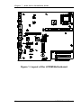
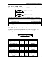
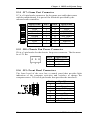
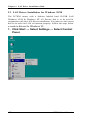
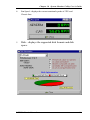
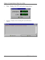
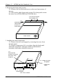
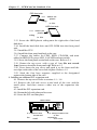
1
LI7WM Socket 370 810E Chipset Custom LPX from Factor Motherboard User's Manual Version 1.0A The brand names, product names and trade names in this manual are trademarks or registered trademarks of their respective holders. This publication is protected by copyright and all rights are reserved. No part of it may be reproduced or transmitted by any means or in any form, without prior consent in writing from the manufacturer. The information in this document has been carefully checked and is believed to be accurate. However, the manufacturer assumes no responsibility for any inaccuracies that may appear in this manual. In no event will the manufacturer be liable for direct, indirect, special, exemplary, incidental or consequential damages resulting from any defect or omission in this manual, even if advised of the possibility of such damages. The material contained herein is for informational purposes only. ii LI7WM User’s Manual Contents Contents Chapter 1 Introduction...................................................5 Chapter 2 Specifications .................................................6 Chapter 3 Hardware Description................................10 3.1 Processor..........................................................................................11 3.2 L2 Cache ..........................................................................................11 3.3 LMA Channels ................................................................................11 3.4 BIOS ...................................................................................................9 3.5 I/O Port Address Map......................................................................9 3.6 Onboard PCI-IDE ...........................................................................9 3.7 Main Memory ...............................................................................10 3.8 Onboard Multi-I/O.............................................................................10 3.9 Interrupt Request (IRQ) Lines ...................................................11 3.10 Onboard VGA ...............................................................................11 3.11 TV-Out .........................................................................................11 3.12 Panel Link Sopport ....................................................................12 3.13 Onboard Ethernet Controller ....................................................12 Chapter 4 Configuring the Motherboard ...................14 4.1 4.2 4.3 4.4 CPU Frequency Selection .............................................................15 Clear CMOS Select: JP11.............................................................15 Onboard Audio Enable/Disable :JP2 ..........................................16 Onboard LAN Enable/Disable :JP3 ............................................16 Chapter 5 Installation...................................................18 5.1 I/O Connectors................................................................................20 5.2 J1: S-VHS Connector.....................................................................20 5.3 J2: RCA Connector........................................................................20 5.4 J3: Panel Link Connector (option)...............................................21 5.5 J4: CRT Connector.........................................................................21 5.6 J5: USB Connector.........................................................................22 5.7 J6/J7: PS/2 Keyboard and PS/2 Mouse Connectors ...............22 5.8 J8/J9: Serial Ports .........................................................................23 5.9 J10: Parallel Port Connector .......................................................23 5.10 J11: RJ45 Connector ..................................................................24 5.11 J J12, J13, J14: Line Out, Line In, Mic Connectors .............24 5.12 J15: IrDA Connector BL21PI Riser Card ..............................24 5.13 J16: OWL (Wake On Lan) Connector ....................................24 5.14 J17: Game Port Connector ........................................................25 5.15 J18: CPU Fan Power Connector ..............................................25 LI7WM User’s Manual iii Contents 5.16 5.17 5.18 5.19 5.20 5.21 5.22 5.23 5.24 5.25 5.26 5.27 5.28 5.29 J19 Front Bezel Connectors........................................................25 J20: ATX Power Supply Connector .......................................26 J21: Floppy Drive Connector ...................................................26 J22,J23: IDE1 and IDE2 Connector ........................................27 J24,J25: CD-ROM Audio In Connector...................................28 J26: Chassis Fan Power Connectors .......................................28 J27: CPU Fan Power Connectors ............................................28 J28: Reset Switch .........................................................................28 JP1:TV-Out: PAL/NTSC............................................................29 JP2: Onboard Audio In Connector............................................29 JP3: Onboard Lan Enable/Disable ............................................29 JP4: Boot Block/Unlock..............................................................30 JP5: Clear CMOS Slect...............................................................30 S1: BL21PI Riser Card Connector............................................30 Chapter 6 BIOS and System Setup .............................32 6.1 BIOS Introduction..........................................................................35 6.2 BIOS Setup......................................................................................35 6.3 Standard CMOS Setup...................................................................37 6.4 BIOS Features Setup......................................................................40 6.5 Advanced Chipset Features Setup .............................................43 6.6 Intergrated Prephierals ................................................................45 6.7 Power Management Setup ..........................................................48 6.8 PNP/PCI Configuration ...............................................................51 6.9 PC Health Status ...........................................................................52 6.10 Frequency/ Voltage Control .....................................................52 6.11 I Load Fail-Safe Defaults ..........................................................54 6.12 Load Optimized Defaults ..........................................................54 6.13 I Set Supervisor / User Password ............................................55 6.14 Save & Exit Setup........................................................................56 6.15 Exit Without Saving.....................................................................56 Chapter 7 Audio Driver Installation Guide ................58 Chapter 8 VGA Driver Installation Guide .................62 Chapter 9 LAN Driver Installation Guide ..................68 Chapter 10 System Monitor Utility User’s Guide .......86 Chapter 11 LI7WM and the Databook Case ...............94 iv LI7WM User’s Manual Chapter 2 Specifications Chapter 1 Introduction This manual is designed to give you information on the LI7WM motherboard. It is divided into the following sections: • Introduction • Specifications • Hardware Description • Configuring the Motherboard • Installation • BIOS and System Setup • Audio Driver Installation Guide • VGA Driver Installation Guide • LAN Driver Installation Guide • System Monitor Utility User’s Guide Checklist Please check that your package is complete and contains the items below. If you discover damaged or missing items, please contact your dealer. • The LI7WM Motherboard with the BL7WM Riser Card • 1 40-pin IDE ribbon cable (14 cm) • 1 40-pin CD-ROM ribbon cable (8 cm) • 1 34-pin FDD ribbon cable (20 cm) • 1 16-pin game port cable LI7WM User’s Manual 5 Chapter 2 Specifications Chapter 2 Specifications The LI7W is a high-performance Intel Celeron (PGA370)/ Pentium III motherboard that offers flexibility in terms of CPU frequency and bus speeds. The main features of the motherboard consist of the following: CPU Socket PGA370 Socket Processor Intel Celeron ( PGA370 ) and Pentium III ( FC-PGA370 ). 300MHz~1GHz L2 Cache CPU integrated L2 cache Chipset Intel 810E (GMCH in 421 BGA and ICH in 241 BGA) Year 2000 Compliant BIOS The onboard Award BIOS is Year 2000 Compliant and will pass software applications that have the tendency to invoke INT1AH function 04H such as year 2000.exe utility released by NSTL. The BIOS comes with ISA Plug and Play (PnP) extension, DMI, bootable CD-ROM and power-management features. Power Connector ATX power supply connector (Use an ATX power supply with 3.3V power.) Onboard Audio Onboard AC97 Codec with external connectors for Line out, Line in, Mic, and Game port. Onboard VGA The highly integrated graphics accelerator consists of dedicated multimedia engines executing in parallel to deliver high performance 3D, 2D and motion compensation video capabilities. The 3D and 2D engines are managed by a 3D/2D pipeline preprocessor allowing a sustained flow of graphics data to be rendered and displayed. It als o features a 4MB display cache buffer. Onboard TV-out connectors support S-VHS and RCA specifications. 6 LI7WM User’s Manual Chapter 2 Specifications TV-Out Chrontel’s CH7007 digital PC to TV encoder is a stand-alone integrated circuit which provides a PC 99 compliant solution for TV output. Suggested for application use with the Intel 810 chipset and Intel 810E chipset, it provides a universal digital input port to accept a pixel data stream from a compatible VGA controller (or equivalent) and converts this directly into NTSC or PAL TV format. Expansion Slots on Riser Card BL7WM Two PCI 32-bit slots Panel Link Support The Sil154 transmitter uses PanelLink® digital technology to support display ranging from VGA to SXGA resolutions (25-112MPps) in a single link interface. The Sil154 transmitter has a highly width 12-bit (1/2 pixel) or 24-bit 1 pixel /clock input for true color (16.7 million) support. In 24-bit mode, the data may be latch on the positive or negative edge of the clock. In 12-bit mode, multiple clocking options exist: with a signal clock, data will be clocked on the falling and the rising edge; with dual clocks data can be clocked on either the falling edge of the rising edge of both clocks. Onboard Ethernet Controller The onboard Intel 82559B Ethernet controller is compatible with both the traditional 10Mbps and advanced 100Mbps LAN facilities. An RJ45 connector and Wake on LAN are supported by LI7WM. DMI BIOS Support Desktop Management Interface (DMI) allows users to download system hardware-level information such as CPU type, CPU speed, internal/external frequencies and memory size. PCI Bus Master IDE Controller (Ultra DMA/33) Supports two connectors for up to four IDE devices in two channels such as ATAPI Tape Backup and CD-ROM drives, PIO Mode 3/4 and Bus Mastering Ultra DMA/33/66 Hard Disk Drives. Super I/O Winbond 83627 HF with 1x ECP, 1x IrDA, 2x UART, 1xfdc, 3x fan, speed monitoring and 7x voltage monitoring and 2x temperature monitoring. Keyboard and Mouse Connectors PS/2 type 7 LI7WM User’s Manual Chapter 2 Specifications USB Connector 2 ports onboard Win95/98 shut-off Allows shut-off control from within Windows 95/98 Modem-ring-on Supports PC powering on through an external modem. Board Dimensions 11.91" x 11.80" (30.3cm x 30.0cm) 8 LI7WM User’s Manual Chapter 2 Specifications Figure 1: Layout of the LI7WM Motherboard 9 LI7WM User’s Manual Chapter 3 Hardware Description Chapter 3 Hardware Description This chapter briefly describes each of the major features of the LI7WM motherboard. The layout of the board in Figure 1 shows the location of the key components. The topics covered in this chapter are as follows: 3.1 Processor..........................................................................................11 3.2 L2 Cache ..........................................................................................11 3.3 BIOS .................................................................................................11 3.4 Main Memory....................................................................................9 3.5 I/O Port Address Map......................................................................9 3.6 DMA Channels .................................................................................9 3.7 Onboard PCI-IDE...........................................................................10 3.8 Interrupt Request (IRQ) Lines......................................................10 3.9 Onboard Multi-I/O .........................................................................11 3.10 Onboard VGA ...............................................................................11 3.11 Onboard Audio .............................................................................12 3.12 Onboard Ethernet Controller (option).......................................13 3.13 Hardware Monitoring IC.............................................................13 LI7WM User’s Manual 10 Chapter 3 3.1 Hardware Description Processor The LI7WM motherboard is designed to take a Intel 810E processor running from 300/ 333/ 366/ 400/ 433/ 466/ 500/ 533/ 566/ 600 to 633MHz at 66MHz CPU bus speed or 550/ 600/ 650/ 700/ 750/ 800/ 850/ 900/ 950MHz at 100MHz CPU bus speed or 600/ 666/ 733/ 800/ 866/ 933 at 133MHz CPU bus speed with its Socket 370 processor connector. 3.2 L2 Cache The L2 cache is integrated in the Intel 810E processor. The private L2 cache bus is not connected to package pins; rather its signals are routed between the two cavities using standard package techniques. 3.3 DMA Channels There are seven DMA channels available on the motherboard. Only DMA2 is used by the floppy controller. In the case that ECP mode on the parallel port is utilized, DMA1 or DMA3 will be used. 3.4 BIOS The BIOS on the LI7WM motherboard provides the standard BIOS functions plus the following additional feature: Power Management The power management feature provides power savings by slowing down the CPU clock, turning off the monitor screen and stopping the HDD spindle motor. The BIOS fully conforms to ACPI (Advanced Configuration and Power Interface) specification. 3.5 Onboard Multi-I/O Onboard AC97 Codec with external connectors for Line out, Line in, Mic, and Game port. 3.6 I/O Port Address Map Each peripheral device in the system is assigned a set of I/O port addresses, which also becomes the identity of the device. There is a total of 1K port address space available. The following table lists the I/O port addresses used on the motherboard. 11 LI7WM User’s Manual Chapter 3 Hardware Description Address 000h - 01Fh 020h - 03Fh 040h - 05Fh 060h - 06Fh 070h - 07Fh 080h - 09Fh 0A0h - 0BFh 0C0h - 0DFh 0F0h 0F1h 1F0h - 1F7h 2F8h - 2FFh 378h - 3FFh 3F0h - 3F7h 3F8h - 3FFh Device Description DMA Controller #1 Interrupt Controller #1 Timer Keyboard Controller Real Time Clock,, NMI DMA Page Register Interrupt Controller #2 DMA Controller #2 Clear Math Copro cessor Busy Signal Reset Math Coprocessor IDE Interface Serial Port #2(COM2) Parallel Port #1(LPT1) Floppy Disk Controller Serial Port #1(COM1) 3.7 Onboard PCI-IDE The PCI-IDE controller is a part of the Intel 810E chipset. It supports PIO mode 3/4 and bus mastering Ultra DMA/33 and DMA/66. The peak transfer rate of PIO mode 3/4 can be as high as 17MB/sec. Using HDDs that support Ultra DMA/33, the peak transfer rate can reach 33 and 66MB/sec. There are two IDE connectors - primary IDE and secondary IDE. With two devices per connector, up to four IDE devices can be supported. 3.8 Main Memory The LI7WM motherboard supports two 168-pin DIMM (Dual In-line Memory Module) sockets to form a memory configuration from 64MB to 512MB. DIMM modules can be 64M and 256MB in SDRAM. In populating the DIMM sockets, any socket can be populated first. Refer to the following table on how to do the memory configuration. (DIMM1) 64MB 128MB 64MB 128MB 128MB 256MB 256MB 256MB 12 (DIMM2) --------64MB 64MB 128MB 64MB 128MB 256MB Total Memory 64MB 128MB 128MB 192MB 256MB 320MB 384MB 512MB LI7WM User’s Manual Chapter 3 Hardware Description 3.9 Interrupt Request (IRQ) Lines There are a total of 15 IRQ lines available on the motherboard. Peripheral devices use an interrupt request to notify the CPU for the service required. The following table shows the IRQ lines used by the devices on the motherboard: Level Function IRQ0 IRQ1 IRQ2 System Timer Output Keyboard Interrupt Cascade Real Time Clock IRQ8 IRQ9 IRQ10 IRQ11 IRQ12 IRQ13 IRQ14 IRQ15 IRQ3 IRQ4 IRQ5 IRQ6 IRQ7 Software Redirected to Int 0Ah or PCI Slot Int# Reserved or PCI Slot Int# Reserved or PCI Slot Int# PS/2 Mouse or PCI Slot Int# Co-Processor Primary IDE Secondary IDE Serial Port #2 Serial Port #1 Parallel Port #2 or PCI Slot Int# Floppy Disk Controller Parallel Port #1 3.10 Onboard VGA The Intel 810E chipset is the result of new design approach to optimize the shared memory architecture while maintaining the cost benefits of integration through Direct AGP and Dynamic Video Memory Technology. a. Direct AGP Direct AGP delivers AGP class graphics performance to PCs at reduced cost. Rather than simply combining two semiconductor cell libraries for component reduction, Intel architects combined the 2D and 3D video capabilities with the memory control unit. This functional overlap within the Graphics and Memory Controller (Intel® 82810E) enables Direct AGP. Direct AGP provides an integrated graphics part with the capability to make direct memory set-up calls (similar to those associated with standard AGP protocol) to system memory. Direct AGP calls can dynamically allocate and de-allocate system memory for complex 3D textures, preserving the benefits of standard AGP add-in solutions. 13 LI7WM User’s Manual Chapter 3 Hardware Description b. Dynamic Video Memory Technology Dynamic Video Memory Technology (DVMT) enables breakthrough graphics and memory performance for all PC segments through Direct AGP and highly efficient memory use. DVMT ensures the most efficient use of all available memory – regardless of whether a frame buffer is present or the size of the main memory– for maximum 3D graphics performance. DVMT also responds to application requirements by automatically allocating the proper amount of display and texturing memory. For example, a 3D application might require more texture memory to enhance the richness of 3D objects. The operating system (OS) views the Intel 810 and 810E chipset driver as an application which uses Direct AGP to request re-allocation of additional memory for 3D applications and returns memory when not required. DVMT is highly scalable — as additional memory is added to the system, more memory will be available to enhance 3D applications. DVMT works dynamically and modulates the bandwidth available to the CPU, graphics and I/O interface, through the intelligent arbitration built into the Intel 82810E. This hard-coded logic evaluates the operating environment and prioritizes traffic to maximize bandwidth for memory intense multimedia applications. c. Memory Usage with DVMT The operating system requires allocation of up to 1Mbyte of system memory to support legacy VGA. System properties will display up to 1Mbyte less than physical system memory available to the operating system. The graphics driver for the Intel 810E/810 chipsets configurations will request up to 4Mbyte of memory from the OS to implement a maximum 1024 x768 screen resolution, 2Mbyte for a command buffer and 4Mbyte used for z-buffering. For high-end 3D applications, the drivers request allocation of system memory from the OS for graphics textures. When the 3D application is closed, the O/S will re-allocate system memory back for generic use. 3.11 TV-Out Chrontel’s CH7007 digital PC to TV encoder is a stand-alone integrated circuit which provides a PC 99 compliant solution for TV output. Suggested application use with the Intel 810 chipset and Intel 810E chipset. It provides a universal digital input port to accept a pixel data stream from a compatible VGA controller (or equivalent) and converts this directly into NTSC or PAL TV format. 14 LI7WM User’s Manual Chapter 3 Hardware Description 3.12 Panel Link Support The Sil154 transmitter uses PanelLink® digital technology to support display ranging from VGA to SXGA resolutions (25-112MPps) in a single link interface. The Sil154 transmitter has a highly with 12-bit (1/2 pixel) or 24-bit 1 pixel /clock input for true color (16.7 million) support. In 24-bit mode, the data may be latch on the positive or negative edge of the clock. In 12-bit mode, multiple clocking options exist: with a signal clock, data will be clocked on the falling and the rising edge; with dual clocks data can be clocked on either the falling edge of the rising edge of both clocks. 3.13 Onboard Ethernet Controller The onboard Intel 82559B Ethernet controller features the following: • PCI local bus • IEEE802.3u auto-negotiation for automatic speed selection • 10/100Mbps operation in a single port PCI bus master architecture • Wake On LAN function support 15 LI7WM User’s Manual Chapter 4 Configuring the Motherboard Chapter 4 Configuring the Motherboard The following sections describe the necessary procedures and proper jumper settings to configure the LI7WM motherboard. For the locations of the jumpers, refer to Figure 2. 4.1 CPU Frequency Selection .............................................................15 4.2 Clear CMOS Select: JP5 .............................................................15 4.3 Onboard Audio Enable/ Disable: JP2 .........................................16 4.4 Onboard Lan Enable/ Disable: JP3..............................................16 The following examples show the conventions used in this chapter. Jumper Open Jumper Closed/Short LI7WM User’s Manual 16 Chapter 4 Configuring the Motherboard 4.1 CPU Frequency Selection Setting CPU Speed in the BIOS Setup The LI7WM motherboard allows users to set the CPU speed through the BIOS Setup. The parameters used in configuring the CPU speed include CPU Clock Multiplier (X3, X3.5, X4, X4.5, X5, X5.5, X6, X6.5, X7, X7.5, X8) and CPU Clock (66MHz, 68MHz, 75MHz, 83MHz or 100MHz, 103MHz, 112MHz, 133MHz). In the initial setup, the system automatically detects the base Frequency of the CPU (66MHz or 100MHz/133MHz). Under the under CPU Speed Setting section, use the ↑ and ↓ keys to easily change the CPU speed or press the PageUp or PageDown key to see more options. Overclocking could cause the system not to boot in the process of setting the CPU speed. When this happens, turn off the computer by pressing the power button and turn it on again by pressing the Insert key and the power button simultaneously. When the system is turned on, press the Delete key to enter BIOS Setup and configure the CPU speed. 4.2 Clear CMOS Select: JP5 Use JP5, to clear the contents of the CMOS RAM. Do not clear the CMOS RAM unless it is absolutely necessary. Before clearing CMOS, you should disconnect the ATX-power connector from the motherboard. JP5 1 2 Jumper Setting Function pin 1-2: short Clear CMOS pin 2-3: short Normal 3 1 17 2 3 LI7WM User’s Manual Chapter 4 Configuring the Motherboard 4.3 JP2: Onboard Audio Enable/Disable Onboard AC ’97 codec support the Audio function. Please refer to the default jumper setting before you proceeding with system installation. JP2 1 2 Jumper Setting Function pin 1-2: short Onboard Audio Disabled pin 2-3: short Onboard Audio Enabled 3 1 4.4 2 3 JP3: Onboard Lan Enable/Disable JP2, a 3-pin header, is the onboard Intel 82559B Ethernet controller. Please refer to the default jumper setting before you proceeding with system installation. JP3 1 2 Jumper Setting Function pin 1-2: short Onboard LAN Disabled pin 2-3: short Onboard Audio Enabled 3 1 18 2 3 LI7WM User’s Manual Chapter 7 Audio Driver Installation Guide Figure 1: Layout of the LI7WM Motherboard 19 LI7WM User’s Manual Chapter 6 BIOS and System Setup Chapter 5 Installation This chapter describes the interface that the LI7WM provides for creating a working system. Refer to Figure 3 for the location of the connectors. The following items are covered in this chapter: 5.1 I/O Connectors................................................................................20 5.2 J1: S-VHS Connector.....................................................................20 5.3 J2: RCA Connector........................................................................20 5.4 J3: Panel Link Connector ............................................................21 5.5 J4: CRT Connector.........................................................................21 5.6 J5: USB Connector.........................................................................22 5.7 J6/J7: PS/2 Keyboard and PS/2 Mouse Connectors.................22 5.8 J8/J9: Serial Ports ...........................................................................23 5.9 J10: Parallel Port Connector.........................................................23 5.10 J11: RJ45 Connector ..................................................................24 5.11 J12, J13, J14: Line Out, Line In, Mic Connectors..................24 5.12 J15: IrDA Connector....................................................................24 5.13 J16: WOL(Wake On Lan)Connector........................................24 5.14 J17: Game Port Connector..........................................................25 5.15 J18: Chassis Fan Power Connector...........................................25 5.16 J19: Front Bezel Connector........................................................25 5.17 J20: ATX Power Supply Connector..........................................26 5.18 J21: Floppy Drive Connector.....................................................26 5.19 J22, J23: IDE1 and IDE2 Connectors.......................................27 5.20 J24, J25: CD-ROM Audio In Connectors................................28 5.21 J26: Chassis Fan Power Connector...........................................28 5.22 J27: CPU Fan Power Connector................................................28 5.23 J28: Reset Switch .........................................................................28 20 LI7WM User’s Manual Chapter 6 BIOS and System Setup 5.24 JP1: TV-Out: PAL/NTSC...........................................................29 5.25 JP2: Onboard Audio In Connector............................................29 5.26 JP3: Onboad Lan Enable/ Disable .............................................29 5.27 JP4: Boot Block Lock/Unlock ...................................................30 5.28 JP5: Clear CMOS Select .............................................................30 5.29 S1: BL7WM Riser Card Connector ......................................30 21 LI7WM User’s Manual Chapter 6 BIOS and System Setup 5.1 I/O Connectors The I/O connectors connect the LI7WM to the most common peripherals. To attach cables to these connectors, carefully align Pin 1 of the cables to that of the connectors. Refer to Figure 4 for the location and orientation of the connectors. Figure 4: Orientation of the I/O Connector 5.2 J1: S-VHS Connector The J1 S-VHS connector is for the TV-Out feature of the onboard VGA controller. Below are the pin-out assignments of the connectors. Pin # 1 2 3 4 Signal Name Ground Ground Luma Output Chroma Output 5.3 J2: RCA Connector The J2 RCA connector is for the TV-Out feature of the onboard VGA controller. 22 LI7WM User’s Manual Chapter 6 BIOS and System Setup 5.4 J3: Panel Link Conne ctor (option) Below are the pin-out assignments of the connectors. Signal Name TXOUT 1+ TXOUT 1Ground Ground TXCLKOUT+ TXCLKOUTGround Vcc No Connect No Connect Pin # 1 2 3 4 5 6 7 8 9 10 Pin # 11 12 13 14 15 16 17 18 19 20 Signal Name TXOUT 2+ TXOUT 2Ground Ground TXOUT 0+ TXOUT 0No Connect Panel detection Panel ID SDA Panel ID SCL 5.5 J4: CRT Connector J4 is a DB-15 VGA connector. The following table shows the pin-out assignments of this connector. Signal Name Red Blue Ground Ground +5V N.C. HSYNC Monitor ID SCL 23 Pin # 1 3 5 7 9 11 13 15 Pin # 2 4 6 8 10 12 14 Signal Name Green N.C. Ground Ground Ground Monitor ID SDA VSYNC LI7WM User’s Manual Chapter 6 BIOS and System Setup 5.6 J5: USB Connector J5 is the standard USB external connector consisting of two ports. USB support allows connections of up to 64 plug and play external peripherals per channel. The following table shows the pin outs of these ports. PORT 2 Pin # 1 2 3 4 Signal Name Vcc USBUSB+ Ground PORT 1 5.7 J6/J7: PS/2 Keyboard and PS/2 Mouse Connectors PS/2 Mouse PS/2 Keyboard Below are the pin-out assignments of the connectors. Signal Name Keyboard data No Connect Ground 5V Keyboard clock No Connect 24 Keyboard 1 2 3 4 5 6 Mouse 1 2 3 4 5 6 Signal Name Mouse data No Connect No Connect 5V Mouse Clock No Connect LI7WM User’s Manual Chapter 6 BIOS and System Setup 5.8 J8/J9: Serial Ports The onboard serial ports of the LI7WM are two DB-9 external connectors. COM1 Serial Port COM2 Serial Port The table below shows the pin-out assignments of these connectors. Signal Name Pin # Pin # Signal Name DCD, Data carrier detect 1 6 DSR, Data set ready RXD, Receive data 2 7 RTS, Request to send TXD, Transmit data 3 8 CTS, Clear to send DTR, Data terminal ready 4 9 RI, Ring indicator GND, ground 5 10 Not Used 5.9 J10: Parallel Port Connector J10 is a DB-25 external connector as seen in the above figure. The following table describes the pin- out assignments of this connector. Signal Name Line printer strobe PD0, parallel data 0 PD1, parallel data 1 PD2, parallel data 2 PD3, parallel data 3 PD4, parallel data 4 PD5, parallel data 5 PD6, parallel data 6 PD7, parallel data 7 ACK, acknowledge Busy Paper empty Select 25 Pin # 1 2 3 4 5 6 7 8 9 10 11 12 13 Pin # 14 15 16 17 18 19 20 21 22 23 24 25 N/A Signal Name AutoFeed Error Initialize Select Ground Ground Ground Ground Ground Ground Ground Ground N/A LI7WM User’s Manual Chapter 6 BIOS and System Setup 5.10 J9: RJ45 Connector (option) This connector is for the 10/100Mbps Ethernet capability of the CPU card. The figure below shows the pin out assignments of this connector and its corresponding input jack. TD+(pin#1) T D-(pin#2) RD+(pin#3) RD-(pin#6) 5.11 J10, J11, J12: Line Out, Line In, Mic Connectors The Line Out (J12), Line In (J13) and Mic (J14) connectors, as shown in the figure below, are used in conjunction with the audio function of the onboard audio controller. 5.12 J15: IrDA Connector This connector is used for an IrDA connector that supports infrared wireless communication. Pin # Signal Name +5V IRRX 1 +5V IRTX 2 No connect 3 Ir RX 4 Ground N.C. GND 5 Ir TX 5.13 WOL(Wake on LAN) Connector: J16 J16 is a 3-pin header for the Wake on LAN function. Wake on LAN will function properly only with an ATX power supply with 5VSB that has 200mA. 1 26 2 3 Pin # 1 2 3 Signal Name +5VSB Ground Wake on LAN LI7WM User’s Manual Chapter 6 BIOS and System Setup 5.14 J17: Game Port Connector J17 is a 16-pin header connector for the game port cable that comes with the motherboard. It is part of the functions provided by the onboard audio controller. Signal Name Vcc JOY4 JOYTIME0 Ground Ground JOYTIME1 JOY5 Vcc Pin # 1 2 3 4 5 6 7 8 Pin # 9 10 11 12 13 14 15 16 Signal Name Vcc JOY6 JOYTIME2 MIDI OUT JOYTIME3 JOY7 MIDI IN No Connect 5.15 J18: Chassis Fan Power Connector J26 is a 3-pin header for the chassis fan power connector. The fan must be a 12V fan. Pin # Signal Name 1 Rotation 2 +12V 1 2 3 3 Ground 5.16 J19: Front Bezel Connectors The front bezel of the case has a control panel that provides light indication of the computer activities and switches to change the computer status. J19 is an 8-pin header that provides the interfaces. Pin # 1 2 3 4 5 6 7 8 27 Signal Name +5V Ground 5VSB LAN Active LED +5V IDE LED Ground Power Button LI7WM User’s Manual Chapter 6 BIOS and System Setup 5.17 J20: ATX Power Supply Connector J20 should be used with an ATX power supply with 3.3V specification. Refer to the table below for the pin out assignments. 11 1 20 10 Signal Name 3.3V -12V Ground PS-ON Ground Ground Ground -5V +5V +5V Pin # 11 12 13 14 15 16 17 18 19 20 Pin # 1 2 3 4 5 6 7 8 9 10 Signal Name 3.3V 3.3V Ground +5V Ground +5V Ground Power good 5VSB +12V 5.18 J21: Floppy Drive Connector J21 of the LI7WM is a 34-pin header and will support up to 2.88MB floppy drives. The following table shows its pin-out assignments. Signal Name Ground Ground Ground Ground Ground Ground Ground Ground Ground Ground Ground Ground Ground Ground Ground Ground Ground 28 Pin # 1 3 5 7 9 11 13 15 17 19 21 23 25 27 29 31 33 Pin # 2 4 6 8 10 12 14 16 18 20 22 24 26 28 30 32 34 Signal Name RM/LC No connect No connect Index Motor enable 0 Drive select 1 Drive select 0 Motor enable 1 Direction Step Write data Write gate Track 00 Write protect Read data Side 1 select Diskette change LI7WM User’s Manual Chapter 6 BIOS and System Setup 5.19 J22, J23: IDE1 and IDE2 Connectors J22: Primary IDE Connector Signal Name Reset IDE Host data 7 Host data 6 Host data 5 Host data 4 Host data 3 Host data 2 Host data 1 Host data 0 Ground DRQ0 Host IOW Host IOR IOCHRDY DACK0 IRQ14 Address 1 Address 0 Chip select 0 Activity Pin # 1 3 5 7 9 11 13 15 17 19 21 23 25 27 29 31 33 35 37 39 Pin # 2 4 6 8 10 12 14 16 18 20 22 24 26 28 30 32 34 36 38 40 Signal Name Ground Host data 8 Host data 9 Host data 10 Host data 11 Host data 12 Host data 13 Host data 14 Host data 15 Key Ground Ground Ground Host ALE Ground No connect Cable ID Address 2 Chip select 1 Ground J23: Secondary IDE Connector Signal Name Reset IDE Host data 7 Host data 6 Host data 5 Host data 4 Host data 3 Host data 2 Host data 1 Host data 0 Ground DRQ0 Host IOW Host IOR IOCHRDY DACK1 MIRQ0 Address 1 Address 0 Chip select 0 Activity 29 Pin # 1 3 5 7 9 11 13 15 17 19 21 23 25 27 29 31 33 35 37 39 Pin # 2 4 6 8 10 12 14 16 18 20 22 24 26 28 30 32 34 36 38 40 Signal Name Ground Host data 8 Host data 9 Host data 10 Host data 11 Host data 12 Host data 13 Host data 14 Host data 15 Key Ground Ground Ground Host ALE Ground No connect Cable ID Address 2 Chip select 1 Ground LI7WM User’s Manual Chapter 6 BIOS and System Setup 5.20 J24, J25: CD-ROM Audio In Connectors J25 and J26 are the onboard CD-ROM audio in connectors. Below are their pin assignments. 1 2 3 4 1 J25 2 3 4 J24 Signal Name Ground Left Ground Right Pin # 1 2 3 4 Pin # 1 2 3 4 Signal Name Right Ground Ground Left 5.21 J26: Chassis Fan Power Connector J26 is a 3-pin header for the chassis fan power connector. The fan must be a 12V fan. Pin # Signal Name 1 Rotation 2 +12V 1 2 3 3 Ground 5.22 J27: CPU Fan Power Connector J27 is a 3-pin header for the CPU fan power connector. The fan must be a 12V fan. 1 2 3 Pin # 1 2 3 Signal Name Rotation +12V Ground 5.23 J28: Reset Switch The reset switch allows the user to reset the system without turning the main power switch off and then on again. 30 LI7WM User’s Manual Chapter 6 BIOS and System Setup 5.24 JP1: TV-Out: PAL/ NTSC Chrontel’s CH7007 digital PC to TV encoder is a stand-alone integrated circuit which provides a PC 99 compliant solution for TV output. It provides a universal digital input port to accept a pixel data stream from a compatible VGA controller (or equivalent) and converts this directly into NTSC or PAL TV format. Below are their pin assignments. JP1 Function JP1 Function PAL NTSC On Off 5.25 JP2: Onboard Audio In Connector JP2, a 3-pin header jumper, is used to enabled/disabled Onboard Software audio. Please refer to the following pin assignment. JP2 1 2 1 3 2 Jumper Setting Function pin 1-2: short Onboard Audio Disabled pin 2-3: short Onboard Audio Enabled 3 5.26 JP3: Onboard LAN Enable/Disable JP3 supports the function of 82559B chip. The table below shows the pin assignments of this connector. JP5 1 1 31 2 2 Setting LAN Function Pin 1-2 Enabled Pin 2-3 Disabled 3 3 LI7WM User’s Manual Chapter 6 BIOS and System Setup 5.27 JP4: Boot Block Lock/Unlock When the Boot Block is locked, BIOS flash update cannot be executed. JP4 Function JP4 Function Boot Block Unlock On Boot Block Locked Off 5.28 JP5: Clear CMOS Select Use JP5, a 3-pin header, to clear the contents of the CMOS RAM. Do not clear the CMOS RAM unless it is absolutely necessary. You will lose your password, etc. JP5 1 1 2 2 3 Jumper Setting Function pin 1-2: short Clear CMOS pin 2-3: short Normal 3 Follow the steps below to clear CMOS data. 1. Disconnect the AC power cord. 2. Short JP12 (1-2) and wait for 3 seconds. 3. Short JP12 (2-3) and replace the AC power cord. 4. Turn on the system. 5.29 S1: BL21PI Riser Card Connector J17 is a slot connector for the BL21PI riser card that comes with the LI7WM motherboard. The riser card comes with one PCI slot. 32 LI7WM User’s Manual Chapter 6 BIOS and System Setup Chapter 6 BIOS and System Setup This chapter describes the different settings available in the Award BIOS. The topics covered in this chapter are as follows: 6.1 BIOS Introduction ..........................................................................35 6.2 BIOS Setup......................................................................................35 6.3 Standard CMOS Setup...................................................................37 Date ....................................................................................................37 Time ...................................................................................................38 Primary HDDs / Secondary HDDs ...............................................38 Drive A / Drive B.............................................................................38 Video..................................................................................................39 Halt On ..............................................................................................39 6.4 BIOS Features Setup......................................................................40 Virus Warning..................................................................................40 CPU Internal Cache / External Cache ..........................................40 CPU L2 Cache ECC Checking......................................................40 Quick Power On Self Test..............................................................41 First/ Secnd/ Third Boot Device................................................... 41 Boot other Device ............................................................................41 Swap Floppy Drive..........................................................................41 Boot Up Floppy Seek......................................................................41 Boot Up NumLock Status..............................................................41 Boot Up System Speed ...................................................................41 Gate A20 Option..............................................................................41 Typematic Rate Setting...................................................................41 Typematic Rate (Chars/Sec)..........................................................42 Typematic Delay (Msec)................................................................42 Security Option ................................................................................42 OS Select for DRAM > 64MB......................................................42 Report No FDD For WIN 95.........................................................42 6.5 Advanced Chipset Features Setup ...............................................43 SDRAM CAS Latency Time .........................................................43 Bank DRAM Timing Trac/Trc ......................................................43 SDRAM RAS-to-CAS Delay ........................................................43 SDRAM RAS Precharge Time ......................................................43 System BIOS Cacheable .................................................................44 Video BIOS Cacheable ...................................................................44 Memory Hole at 15MB - 16MB....................................................44 CPU-Lantency Timer ....................................................................44 Delayed Transaction........................................................................44 33 LI7WM User’s Manual Chapter 6 BIOS and System Setup OnChip Video Window Size .........................................................44 Onboard Display Cache Setting ....................................................44 6.6 Intergrated Perphierals ................................................................45 Onchip Primary/Secondry PCI IDE..........................................45 IDE Primary/Secondary Master /Slave PIO ................................45 IDE Primary/Secondary Master /Slave UDMA .........................46 USB Controller ..............................................................................46 USB Keyboard Suppory ...............................................................46 Init Display First ............................................................................46 AC97 Video ......................................................................................46 AC97 Modem .................................................................................46 IDE HDD Block Modem ..............................................................46 Power on Function .........................................................................46 Onboard FDD Controller................................................................46 Onboard Serial/Parallel Port ........................................................47 UART Mode select..........................................................................47 Onboard Parallel Port ......................................................................47 RxD, TxD Delay ..............................................................................47 UR2 Duplex mode ...........................................................................47 Use IR Pins ...................................................................................47 PWRON after PW-Fail ...................................................................47 Game Adress.....................................................................................47 Midi Port Adress..............................................................................47 Midi Port IRQ...................................................................................47 6.7 Power Management Set.................................................................48 ACPI Function..................................................................................48 ACPI Suspend Type........................................................................48 Power Management .......................................................................48 Video Off Method............................................................................49 Video Off in Suspend ....................................................................49 Suspend Type...................................................................................49 Modem Use IRQ..............................................................................49 Suspend Mode...............................................................................49 HDD Power down............................................................................49 Safe-Off by PWR-BTTN ............................................................49 Wake-Up by PCI Card ..................................................................49 PWR On by Modem/Lan ..............................................................50 CPU Thermal-Throttling ..............................................................50 Resume by Alarm ..........................................................................50 Reload Global Timer Events .......................................................50 6.8 PNP/PCI C onfiguation .................................................................51 Reset Configuation Date ..............................................................51 34 LI7WM User’s Manual Chapter 6 BIOS and System Setup Resource Controller By ................................................................51 IRQ Resource ...................................................................................51 PCI/VGA Palette Snoop.................................................................51 6.9 PC Health Status ...........................................................................52 Tempreature/ Fan Speeds/ Voltage .............................................52 Shutdown Tempreature ...................................................................52 6.10 Frequency/ Voltage Control .......................................................52 Auto Detect DIMM/PCI Clk..........................................................53 Spread Sprctum ..............................................................................53 Host CPU/PCI Clock.......................................................................53 CPU Clock Ratio..............................................................................53 6.11 Lord Fail- Safe Default ...............................................................54 6.12 Lord Optimized Default ..............................................................54 6.13 Set Superior/ User Password ......................................................55 6.14 Save & Exit Setup........................................................................56 6.15 Exit Without Saving.....................................................................56 35 LI7WM User’s Manual Chapter 6 BIOS and System Setup 6.1 BIOS Introduction The Award BIOS (Basic Input/Output System) installed in your computer system’s ROM supports Intel Celeron processors. The BIOS provides critical low-level support for a standard device such as disk drives, serial and parallel ports. It also adds virus and password protection as well as special support for detailed fine-tuning of the chipset controlling the entire system. 6.2 BIOS Setup The Award BIOS provides a Setup utility program for specifying the system configurations and settings. The BIOS ROM of the system stores the Setup utility. When you turn on the computer, the Award BIOS is immediately activated. Pressing the <Del> key immediately allows you to enter the Setup utility. If you are a little bit late pressing the <Del> key, POST (Power On Self Test) will continue with its test routines, thus preventing you from invoking the Setup. If you still wish to enter Setup, restart the system by pressing the ”Reset” button or simultaneously pressing the <Ctrl>, <Alt> and <Delete> keys. You can also restart by turning the system Off and back On again. The following message will appear on the screen: Press <DEL> to Enter Setup In general, you press the arrow keys to highlight items, <Enter> to select, the <PgUp> and <PgDn> keys to change entries, <F1> for help and <Esc> to quit. When you enter the Setup utility, the Main Menu screen will appear on the screen. The Main Menu allows you to select from various setup functions and exit choices. ROM PCI/ISA BIOS CMOS SETUP UTILITY AWARD SOFTWARE, INC. Standard CMOS Features Frequency/Voltage Control Advanced BIOS Features Load Fail-Safe Defaults Advanced Chipset Features Load Optimized Defaults Integrated Peripherals Set Supervisor Password Power Management Setup Set User Password PnP/PCI Configurations Save & Exit Setup PC Health Status Exit Without Saving ESC : Quit á â à ß : Select Item F10 : Save & Exit Setup Time, Date, Hard Disk Type… 36 LI7WM User’s Manual Chapter 6 BIOS and System Setup The section below the setup items of the Main Menu displays the control keys for this menu. Another section at the bottom of the Main Menu just below the control keys section displays information on the currently highlighted item in the list. NOTE: After making and saving system changes with Setup, you find that your computer cannot boot, the Award BIOS supports an override to the CMOS settings that resets your system to its default. We strongly recommend that you avoid making any changes to the chipset defaults. These defaults have been carefully chosen by both Award and your system manufacturer to provide the absolute maximum performance and reliability. 37 LI7WM User’s Manual Chapter 6 BIOS and System Setup 6.3 Standard CMOS Setup “Standard CMOS Setup” choice allows you to record some basic hardware configurations in your computer system and set the system clock and error handling. If the motherboard is already installed in a working system, you will not need to select this option. You will need to run the Standard CMOS option, however, if you change your system hardware configurations, the onboard battery fails, or the configuration stored in the CMOS memory was lost or damaged. CMOS Setup Utility – Copyright © 1984-1999 Award Software Standard CMOS Features Date (mm:dd:yy) Tue, Mar 26 1999 Time (hh:mm:ss) 00 : 00 : 00 Menu Level Item Help IDE Primary Master IDE Primary Slave IDE Secondary Master IDE Secondary Slave Press Enter 13020 MB Press Enter None Press Enter None Press Enter None Change the day, month, Year and century Drive A Drive B 1.44M, 3.5 in. None Video Halt On Base Memory Extended Memory Total Memory EGA/VGA All Errors 640K 129024K 130048K At the bottom of the menu are the control keys for use on this menu. If you need any help in each item field, you can press the <F1> key. It will display the relevant information to help you. The memory display at the lower right-hand side of the menu is read-only. It will adjust automatically according to the memory changed. The following describes each item of this menu. Date The date format is: Day : Month : Date : Year : Sun to Sat 1 to 12 1 to 31 1994 to 2079 To set the date, highlight the “Date” field and use the PageUp/ PageDown or +/- keys to set the current time. 38 LI7WM User’s Manual Chapter 6 BIOS and System Setup Time The time format is: Hour : 00 to 23 Minute : 00 to 59 Second : 00 to 59 To set the time, highlight the “Time” field and use the <PgUp>/ <PgDn> or +/- keys to set the current time. IDE Primary HDDs / IDE Secondary HDDs The onboard PCI IDE connectors provide Primary and Secondary channels for connecting up to four IDE hard disks or other IDE devices. Each channel can support up to two hard disks; the first is the “Master” and the second is the “Slave”. Press <Enter> to configure the hard disk. The selections include Auto, Manual, and None. Select ‘Manual’ to define the drive information manually. You will be asked to enter the following items. CYLS : Number of cylinders HEAD : Number of read/write heads PRECOMP : Write precompensation LANDZ : Landing zone SECTOR : Number of sectors SIZE : Automatically adjust according to the configuration The Access Mode selections are as follows: Auto Normal (HD < 528MB) Large (for MS-DOS only) LBA (HD > 528MB and supports Logical Block Addressing) Drive A / Drive B These fields identify the types of floppy disk drive A or drive B that has been installed in the computer. The available specifications are: 360KB 1.2MB 720KB 1.44MB 2.88MB 5.25 in. 5.25 in. 3.5 in. 3.5 in. 3.5 in. NOTE: The specifications of your drive must match with the drive table. The hard disk will not work properly if you enter incorrect information in these fields. If your hard disk drive type is not matched or listed, you can use Type User to define your own drive type manually. 39 LI7WM User’s Manual Chapter 6 BIOS and System Setup Video This field selects the type of video display card installed in your system. You can choose the following video display cards: EGA/VGA For EGA, VGA, SEGA, SVGA or PGA monitor adapters. (default) CGA 40 Power up in 40 column mode. CGA 80 Power up in 80 column mode. MONO For Hercules or MDA adapters. Halt On This field determines whether or not the system will halt if an error is detected during power up. No errors The system boot will not be halted for any error that may be detected. All errors Whenever the BIOS detects a non-fatal error, the system will stop and you will be prompted. All, But Keyboard The system boot will not be halted for a keyboard error; it will stop for all other errors All, But Diskette The system boot will not be halted for a disk error; it will stop for all other errors. All, But Disk/Key The system boot will not be halted for a keyboard or disk error; it will stop for all others. 40 LI7WM User’s Manual Chapter 6 BIOS and System Setup 6.4 Advanced BIOS Features Setup This section allows you to configure and improve your system and allows you to set up some system features according to your preference. CMOS Setup Utility – Copyright © 1984-1999 Award Software Advanced BIOS Features Virus Warning CPU Internal Cache External Cache CPU L2 Cache ECC Checking Quick Power On Self Test First Boot Device Second Boot Device Third Boot Device Boot Other Device Swap Floppy Drive Boot Up Floppy Seek Boot Up Numlock Status Gate A20 Option Typematic Rate Setting Typematic Rate (chars/Sec) Typematic Delay (Msec) Security Option OS Select For DRAM>64MB Report No FDD For WIN 95 Disabled Enabled Enabled Enabled Enabled Floppy HDD-0 LS/ZIP Enabled Disabled Disabled On Fast Disabled 6 250 Setup Non-OS2 Yes ITEM HELP Menu Level Allows you choose the VIRUS warning feature for IDE Hard Disk boot sector protection. If this function is enabled and someone attempt to write data into this area, BIOS will show a warning message on screen and alarm beep Virus Warning This item protects the boot sector and partition table of your hard disk against accidental modifications. If an attempt is made, the BIOS will halt the system and display a warning message. If this occurs, you can either allow the operation to continue or run an anti-virus program to locate and remove the problem. NOTE: Many disk diagnostic programs, which attempt to access the boot sector table, can cause the virus warning. If you will run such a program, disable the Virus Warning feature. CPU Internal Cache / External Cache Cache memory is additional memory that is much faster than conventional DRAM (system memory). CPUs from 486-type on up contain internal cache memory, and most, but not all, modern PCs have additional (external) cache memory. When the CPU requests data, the system transfers the requested data from the main DRAM into cache memory, for even faster access by the CPU. These items allow you to enable (speed up memory access) or disable the cache function. By default, these items are Enabled. CPU L2 Cache ECC Checking This field enables or disables the ECC (Error Correction Checking) checking of the CPU level-2 cache. The default setting is Enabled. 41 LI7WM User’s Manual Chapter 6 BIOS and System Setup Quick Power On Self Test When enabled, this field speeds up the Power On Self Test (POST) after the system is turned on. If it is set to Enabled, BIOS will skip some items. First/Second/Third Boot Device These fields determine the drive that the system searches first for an operating system. The options available include Floppy, LS/ZIP, HDD-0, SCSI, CDROM, HDD-1, HDD-2, HDD-3, LAN and Disable. Boot Other Device These fields allow the system to search for an operating system from other devices other than the ones selected in the First/Second/Third Boot Device. Swap Floppy Drive This item allows you to determine whether or not to enable Swap Floppy Drive. When enabled, the BIOS swaps floppy drive assignments so that Drive A becomes Drive B, and Drive B becomes Drive A. By default, this field is set to Disabled. Boot Up Floppy Seek When enabled, the BIOS will seek whether or not the floppy drive installed has 40 or 80 tracks. 360K type has 40 tracks while 760K, 1.2M and 1.44M all have 80 tracks. By default, this field is set to Enabled. Boot Up NumLock Status This allows you to activate the NumLock function after you power up the system. By default, the system boots up with NumLock On. Boot Up System Speed This has no function and selects the default system speed (High). Gate A20 Option This field allows you to select how Gate A20 is worked. Gate A20 is a device used to address memory above 1 MB. The default setting is Fast. Typematic Rate Setting When disabled, continually holding down a key on your keyboard will generate only one instance. When enabled, you can set the two typematic controls listed next. By default, this field is set to Disabled. 42 LI7WM User’s Manual Chapter 6 BIOS and System Setup Typematic Rate (Chars/Sec) When disabled, continually holding down a key on your keyboard will generate only one instance. When enabled, you can set the two typematic controls listed next. By default, this field is set to Disabled. Typematic Delay (Msec) When the typematic rate is enabled, this item allows you to set the time interval for displaying the first and second characters. By default, this item is set to 250msec. Security Option This field allows you to limit access to the System and Setup. The default value is Setup. When you select System, the system prompts for the User Password every time you boot up. When you select Setup, the system always boots up and prompts for the Supervisor Password only when the Setup utility is called up. OS Select for DRAM > 64MB This option allows the system to access greater than 64MB of DRAM memory when used with OS/2 that depends on certain BIOS calls to access memory. The default setting is Non-OS/2. Report No FDD For WIN 95 This option allows Windows 95 to share with other peripherals IRQ6, which is assigned to a floppy disk drive if the drive is not exist. 43 LI7WM User’s Manual Chapter 6 BIOS and System Setup 6.5 Advanced Chipset Features Setup This Setup menu controls the configuration of the motherboard chipset. CMOS Setup Utility – Copyright © 1984-1999 Award Software Advanced Chipset Features SDRAM CAS Latency Time SDRAM Cycle Time Tras/Trc SDRAM RAS-to-CAS Delay SDRAM RAS Precharge Time System BIOS Cacheable Video BIOS Cacheable Memory Hole At 15M-16M CPU Latency Timer Delayed Transaction On-Chip Video Window Size Auto 6/8 3 3 Enabled Enabled Disabled Enabled Enabled 64MB * Onboard Display Cache Setting * CAS# Latency Paging Mode Control RAS-to-CAS Override RAS# Timing RAS# Precharge Timing 3 Open By CAS# LT Fast Fast ITEM HELP Menu Level SDRAM CAS Latency Time You can select CAS latency time in HCLKs of 2/2 or 3/3. The system board designer should set the values in this field, depending on the DRAM installed. Do not change the values in this field unless you change specifications of the installed DRAM or the installed CPU. The choices are Auto, 2 and 3. SDRAM Cycle Time Tras/Trc The settings available for the SDRAM Cycle Time Tras/Trc are 6/8 and 5/7. The default setting is 6/8. SDRAM RAS-to-CAS Delay You can select RAS to CAS Delay time in HCLKs of 2/2 or 3/3. The system board designer should set the values in this field, depending on the DRAM installed. Do not change the values in this field unless you change specifications of the installed DRAM or the installed CPU. The choices are 2 and 3. SDRAM RAS Precharge Time This option defines the length of time for Row Address Strobe is allowed to precharge. The choices are 2 and 3. System BIOS Cacheable The setting of Enabled allows caching of the system BIOS ROM at F000h -FFFFFh, resulting in better system performance. However, if any program writes to this memory area, a system error may result. 44 LI7WM User’s Manual Chapter 6 BIOS and System Setup Video BIOS Cacheable The Setting Enabled allows caching of the video BIOS ROM at C0000h-F7FFFh, resulting in better video performance. However, if any program writes to this memory area, a system error may result. Memory Hole At 15M-16M In order to improve performance, certain space in memory can be reserved for ISA cards. This memory must be mapped into the memory space below 16 MB. The choices are Enabled and Disabled. CPU Latency Timer This field enable or disable the CPU latency timer. The default setting is Enabled. Delayed Transaction The chipset has an embedded 32-bit posted write buffer to support delay transactions cycles. Select Enabled to support compliance with PCI specification version 2.1. On-Chip Video Window Size The setting choices for the On-Chip Video Window Size are 64MB and 32MB. By default, this option is set to 64MB. Onboard Display Cache Setting The default setting and optional setting for the onboard display cache functions are as follows: CAS# Latency 3(default), 2(option) Paging Mode Control Open (default), Close (option) RAS-to-CAS Override by CAS# LT (default), Override (2)(option) RAS# Timing Fast (default), Slow (option) RAS# Precharge Timing Fast (default), Slow (option) 45 LI7WM User’s Manual Chapter 6 BIOS and System Setup 6.6 Integrated Peripherals This section sets configurations for your hard disk and other integrated peripherals. CMOS Setup Utility – Copyright © 1984-1999 Award Software Advanced Chipset Features On-Chip Primary PCI IDE On-Chip Secondary PCI IDE IDE Primary Master PIO IDE Primary Slave PIO IDE Secondary Master PIO IDE Secondary Slave PIO IDE Primary Master UDMA IDE Primary Slave UDMA IDE Secondary Master UDMA IDE Secondary Slave UDMA USB Controller USB Keyboard Support Init Display First AC97 Audio AC97 Modem IDE Block Mode POWER ON Function KB Power ON Password Hot Key Power ON Onboard FDC Controller Onboard Serial Port 1 Onboard Serial Port 2 UART Mode Select RxD, TxD Active IR Transmission Delay UR2 Duplex Mode Use IR Pins Onboard Parallel Port Parallel Port Mode EPP Mode Select ECP Mode Use DMA PWRON After PWR-Fail Game Port Address Midi Port Address Midi Port IRQ Enabled Enabled Auto Auto Auto Auto Auto Auto Auto Auto Enabled Disabled PCI Slot Enabled Disabled Enabled Button Only Enter Ctrl-F1 Enabled 3F8/IRQ4 2F8/IRQ3 Normal Hi, Lo Enabled Half (Full) IR, Rx2Tx2 378/IRQ7 SPP EPP1.7 3 Off 201 330 10 ITEM HELP Menu Level OnChip Primary/Secondary PCI IDE The integrated peripheral controller contains an IDE interface with support for two IDE channels. Select Enabled to activate the channels. IDE Primary/Secondary Master/Slave PIO These fields allow your system hard disk controller to work faster. Rather than have the BIOS issue a series of commands that transfer to or from the disk drive, PIO (Programmed Input/Output) allows the BIOS to communicate with the controller and CPU directly. The system supports five modes, numbered from 0 (default) to 4, which primarily differ in timing. When Auto is selected, the BIOS will select the best available mode. 46 LI7WM User’s Manual Chapter 6 BIOS and System Setup IDE Primary/Secondary Master/Slave UDMA These fields allow your system to improve disk I/O throughput to 66Mb/sec with the Ultra DMA/66 feature. The options are Auto and Disabled. USB Controller The options for this field are Enabled and Disabled. By default, this field is set to Enabled. USB Keyboard Support By default, the USB Keyboard Support field is set to Disabled. Init Display First This field allows the system to initialize first the VGA card on chip or the display on the PCI Slot. By default, the PCI Slot VGA is initialized first. AC97 Audio By default, the AC97 Audio is set to Enabled. AC97 Modem By default, the AC97 Modem is set to Disabled. IDE HDD Block Mode This field allows your hard disk controller to use the fast block mode to transfer data to and from your hard disk drive. POWER ON Function This field allows powering on by the following methods: Password Hot KEY Keyboard 98 BUTTON ONLY Onboard FDD Controller Select Enabled if your system has a floppy disk controller (FDC) installed on the motherboard and you wish to use it. If you install an add-in FDC or the system has no floppy drive, select Disabled in this field. This option allows you to select the onboard FDD port. 47 LI7WM User’s Manual Chapter 6 BIOS and System Setup Onboard Serial/Parallel Port These fields allow you to select the onboard serial and parallel ports and their addresses. The default values for these ports are: Serial Port 1 3F8/IRQ4 Serial Port 2 2F8/IRQ3 Parallel Port 378H/IRQ7 UART Mode Select This field determines the UART mode in your computer. The default value is Normal. Other options include IrDA and ASKIR. Onboard Parallel Port The setting for this field are 378/IRQ7, 278/IRQ5, 2BC/IRA7 and Disabled. By default, the onboard parallel port is set to 378/IRQ7. Onboard Parallel Port The setting for this field are 378/IRQ7, 278/IRQ5, 2BC/IRA7 and Disabled. By default, the onboard parallel port is set to 378/IRQ7. RxD, TxD Active The settings for this field are Hi,Lo, Lo,Hi, Lo,Lo, and Hi,Hi. IR Transmission Delay By default, this field is set to Enabled. UR2 Duplex Mode The settings available for this field are Half (default) and Full. Use IR Pins The settings for this field are IR, Rx2Tx2 (default) and RxD2, TxD2. PWRON After PW-Fail In case of power failure, the system can be configured to power on or to remain off when the power returns. These two settings are Former-Sts and Off respectively. The default setting for this field is Off. Game Port Address The settings for this field are 201 (default), 209 and Disabled. Midi Port Address The option settings for this field are 330, 300, 290 and Disabled. The default setting is 330. Midi Port IRQ The option settings for this field are 5 and 7. The default setting is 7. 48 LI7WM User’s Manual Chapter 6 BIOS and System Setup 6.7 Power Management Setup The Power Management Setup allows you to save energy of your system effectively. It will shut down the hard disk and turn off video display after a period of inactivity. CMOS Setup Utility – Copyright © 1984-1999 Award Software Power Management Setup ACPI Function Enabled ACPI Suspend Type Power Management Video Off Method Video Off In Suspend Suspend Type Modem Use IRQ Suspend Mode HDD Power Down Soft-Off by PWR-BTTN Wake-Up by PCI Card PW On by Modem/LAN CPU Thermal-Throttling Resume by Alarm Date (of Month) Alarm Time (hh:mm:ss) Alarm S1 (POS) User Define DPMS Yes Stop Grant 3 Disabled Disabled Instant-Off Disabled Enabled 62.5% Disabled 0 0 ** Reload Global Timer Events ** Primary IDE 0 Primary IDE 1 Secondary IDE 0 Secondary IDE 1 FDD, COM, LPT Port PCI PIRQ[A-D] # Disabled Disabled Disabled Disabled Disabled Disabled ITEM HELP Menu Level ACPI Function This field allows you to enable or disable the ACPI (Advanced Configuration Power Interface) function on the motherboard. By default, this field is set to Disabled ACPI Suspend Type The options for the ACPI Suspend Type field are S1(POS) and S3(STR). The default setting for this field is S1(POS). Note: The S3(STR) hardware is optional. Power Management This field allows you to select the type of power saving management modes. There are four selections for Power Management. Min. Power Saving Minimum power management Max. Power Saving Maximum power management. User Define Each of the ranges is from 1 min. to 1hr. Except for HDD Power Down which ranges from 1 min. to 15 min. (Default) 49 LI7WM User’s Manual Chapter 6 BIOS and System Setup NOTE: In order to enable the CPU overheat protection feature, the Power Management field should not be set to Disabled. Video Off Method This field defines the Video Off features. There are three options. V/H SYNC + Blank Default setting, blank the screen and turn off vertical and horizontal scanning. DPMS Allows the BIOS to control the video display card if it supports the DPMS feature. Blank Screen This option only writes blanks to the video buffer. Video Off in Suspend When enabled, the video is off in suspend mode. The default setting is Yes. Suspend Type The settings for this field are Stop Grant (default) and PwrOn Suspend. Modem Use IRQ This field sets the IRQ used by the Modem. By default, the IRQ used is 3. Suspend Mode When enabled, and after the set time of system inactivity, all devices except the CPU will be shut off. HDD Power Down When enabled, and after the set time of system inactivity, the hard disk drive will be powered down while all other devices remain active. Soft-Off by PWR-BTTN This field defines the power-off mode when using an ATX power supply. The Instant Off mode allows powering off immediately upon pressing the power button. In the Delay 4 Sec mode, the system powers off when the power button is pressed for more than four seconds or enters the suspend mode when pressed for less than 4 seconds. The default value is Instant Off. Wake-Up by PCI Card The settings for this field are Enabled and Disabled (default). 50 LI7WM User’s Manual Chapter 6 BIOS and System Setup PWR On by Modem/LAN This field enables or disables the power on of the system through the modem connected to the serial port or LAN. CPU Thermal-Throttling The CPU Thermal Throttling function, by default, is set to 62.5% Resume by Alarm This field enables or disables the resumption of the system operation. When enabled, the user is allowed to set the Date and Time. Reload Global Timer Events The HDD, FDD, COM, LPT Ports, and PCI PIRQ are I/O events which can prevent the system from entering a power saving mode or can awaken the system from such a mode. When an I/O device wants to gain the attention of the operating system, it signals this by causing an IRQ to occur. When the operating system is ready to respond to the request, it interrupts itself and performs the service. 51 LI7WM User’s Manual Chapter 6 BIOS and System Setup 6.8 PNP/PCI Configuration This option configures the PCI bus system. All PCI bus systems on the system use INT#, thus all installed PCI cards must be set to this value. CMOS Setup Utility – Copyright © 1984-1999 Award Software PnP/PCI Configurations Reset Configuration Data Disabled Resources Controlled By IRQ Resources Auto (ESCD) Press Enter PCI/VGA Palette Snoop Disabled ITEM HELP Menu Level Default is Disabled. Select Enabled to reset Extended System Configuration Data (ESCD) when you exit Setup if you have installed a new add-on and the system reconfiguration has caused such a serious conflict that the OS cannot boot Reset Configuration Data This field allows you to determine whether to reset the configuration data or not. The default value is Disabled. Resources Controlled By The settings for this field are Auto (ESCD) (default) and Manual. IRQ Resources To configure the IRQ Resources, the Resource Controlled By field should be set to Manual. PCI/VGA Palette Snoop Some non-standard VGA display cards may not show colors properly. This field allows you to set whether or not MPEG ISA/VESA VGA Cards can work with PCI/VGA. When this field is enabled, a PCI/VGA can work with an MPEG ISA/VESA VGA card. When this field is disabled, a PCI/VGA cannot work with an MPEG ISA/VESA Card. 52 LI7WM User’s Manual Chapter 6 BIOS and System Setup 6.9 PC Health Status This section shows the parameters in determining the PC Health Status. These parameters include temperatures, fan speeds and voltages. CMOS Setup Utility – Copyright © 1984-1999 Award Software PC Health Status CPU Warning Temperature 66°C/151°F Current System Temp. Current CPU Temperature Current CPUFAN Speed Current AMR/PCI Speed Current Chassis FAN Speed VCCP(V) +1.8V(V) +3.3V (V) + 5V +12 V -12 V - 5V VBAT (V) 5VSB (V) Shutdown Temperature 32°C/89°F 38°C/100°F 4470 RPM 0 RPM 0 RPM 1.98 V 1.76 V 3.34 V 4.97 V 11.91V 12.03V 5.04 V 3.50 V 5.29 V ITEM HELP 75°C/167°F Temperatures/Fan Speeds/Voltages These fields are the parameters of the hardware mo nitoring function feature of the motherboard. The values are read-only values as monitored by the system and show the PC health status. Shutdown Temperature This field allows the user to set the temperature by which the system automatically shuts down once the threshold temperature is reached. This function can help damage to the system that is caused by overheating. 6.10 Frequency/Voltage Control This section shows the user how to configure the key components. CMOS Setup Utility – Copyright © 1984-1999 Award Software Frequency/Voltage Control Auto Detect DIMM/PCI Clk Disabled Spread Spectrum Host CPU/PCI Clock CPU Clock Ratio Disabled Default X3 53 ITEM HELP Menu Level LI7WM User’s Manual Chapter 6 BIOS and System Setup Auto Detect DIMM/PCI Clk The settings for this field are Enabled and Disabled (default). Spread Spectrum This field sets the value of the spread spectrum. The default setting is Disabled. This field is for CE testing use only . Host CPU/PCI Clock The Host CPU/PCI Clock has a default setting of Default which is either 66/33MHz or 100/33MHz as automatically detected by the system. The options are as follows: For CPU with 66MHz FSB, the options are 66/33MHz (Default), 75/37MHz, and 80/40 MHz. For CPU with 100MHz FSB, options are 100/33MHz (Default), 112/37MHz, 117/39MHz, 129/43MHz, 133/33MHz, 138/46MHz, 140/35MHz, 150/37MHz, 166/41MHz, 180/30MHz, 190/31MHz and 200/33MHz. NOTE: Overclocking could cause the system not to boot. When this happens, turn off the computer by pressing the power button and turn it on again by pressing the Insert key and the power button simultaneously. Then press the Delete key to enter BIOS Setup and configure the CPU speed. CPU Clock Ratio The CPU Ratio, also known as the CPU bus speed multiplier, can be configured as 3, 3.5, 4, 4.5, 5, 5.5, 6, 6.5, 7, 7.5, and 8. The above setup is for Intel 810E chipset use only. For motherboards with Intel 810 (MI6WBML), the options for Spread Spectrum and Host CPU/PCI Clock are not available. An extra option is the CPU Clock/SpreadSpectrum. The setting for the CPU Clock is 66MHz~150MHz, while the settings for Spread Spectrum are off and on. 54 LI7WM User’s Manual Chapter 6 BIOS and System Setup 6.11 Load Fail-Safe Defaults This option allows you to load the troubleshooting default values permanently stored in the BIOS ROM. These default settings are non-optimal and disable all high-performance features. CMOS Setup Utility – Copyright © 1984-1999 Award Software Load Fail-Safe Defaults Standard CMOS Features Advanced BIOS Features Advanced Chipset Features Integrated Peripherals Power Management Setup PnP/PCI Configurations PC Health Status ESC : Quit Frequency/Voltage Control Load Fail-Safe Defaults Load Optimized Defaults Set Supervisor Password Set User Password Save & Exit Setup Exit Without Saving á â à ß : Select Item F10 : Save & Exit Setup 6.12 Load Optimized Defaults This option allows you to load the default values to your system configuration. These default settings are optimal and enable all high performance features. CMOS Setup Utility – Copyright © 1984-1999 Award Software Load Optimized Defaults Standard CMOS Features Advanced BIOS Features Advanced Chipset Features Integrated Peripherals Power Management Setup PnP/PCI Configurations PC Health Status ESC : Quit F10 : Save & Exit Setup 55 Frequency/Voltage Control Load Fail-Safe Defaults Load Optimized Defaults Set Supervisor Password Set User Password Save & Exit Setup Exit Without Saving á â à ß : Select Item LI7WM User’s Manual Chapter 6 BIOS and System Setup 6.13 Set Supervisor/User Password These two options set the system password. Supervisor Password sets a password that will be used to protect the system and Setup utility. User Password sets a password that will be used exclusively on the system. To specify a password, highlight the type you want and press <Enter>. The Enter Password: message prompts on the screen. Type the password, up to eight characters in length, and press <Enter>. The system confirms your password by asking you to type it again. After setting a password, the screen automatically returns to the main screen. To disable a password, just press the <Enter> key when you are prompted to enter the password. A message will confirm the password to be disabled. Once the password is disabled, the system will boot and you can enter Setup freely. CMOS Setup Utility – Copyright © 1984-1999 Award Software Standard CMOS Features Advanced BIOS Features Advanced Chipset Features Integrated Peripherals Power Management Setup PnP/PCI Configurations PC Health Status ESC : Quit F10 : Save & Exit Setup 56 Frequency/Voltage Control Load Fail-Safe Defaults Load Optimized Defaults Set Supervisor Password Set User Password Save & Exit Setup Exit Without Saving á â à ß : Select Item LI7WM User’s Manual Chapter 6 BIOS and System Setup 6.14 Save & Exit Setup This option allows you to determine whether or not to accept the modifications. If you type “Y”, you will quit the setup utility and save all changes into the CMOS memory. If you type “N”, you will return to Setup utility. CMOS Setup Utility – Copyright © 1984-1999 Award Software Save & Exit Setup Standard CMOS Features Advanced BIOS Features Advanced Chipset Features Integrated Peripherals Power Management Setup PnP/PCI Configurations PC Health Status ESC : Quit F10 : Save & Exit Setup Frequency/Voltage Control Load Fail-Safe Defaults Load Optimized Defaults Set Supervisor Password Set User Password Save & Exit Setup Exit Without Saving á â à ß : Select Item 6.15 Exit Without Saving Select this option to exit the Setup utility without saving the changes you have made in this session. Typing “Y” will quit the Setup utility without saving the modifications. Typing “N” will return you to Setup utility. CMOS Setup Utility – Copyright © 1984-1999 Award Software Exit Without Saving Standard CMOS Features Advanced BIOS Features Advanced Chipset Features Integrated Peripherals Power Management Setup PnP/PCI Configurations PC Health Status ESC : Quit F10 : Save & Exit Setup 57 Frequency/Voltage Control Load Fail-Safe Defaults Load Optimized Defaults Set Supervisor Password Set User Password Save & Exit Setup Exit Without Saving á â à ß : Select Item LI7WM User’s Manual Chapter 7 Audio Driver Installation Guide Chapter 7 Audio Driver Installation Guide This chapter describe the audio driver installation procedure for the onboard Intel 810E + AC97. With a PCI Bus Mastering interface with DOS compatibility, it supports 32 voices wavetable, surround sound, 3D audio, and audio effects such as reverb and chorus. Creative Labs ES1373 uses single, shareable PCI interrupt and is AC97 compliant. For normal operations and to maximize the audio functions of the motherboard, follow the audio driver installation procedure below. Installing The Audio Drivers For Windows 95/98 For Analog Device AC97 Codec Audio Driver (CD Ver. 1.8) If the CD that comes with your motherboard is Ver. 1.8, complete steps 1-4. If the CD is Ver. 1.9, run the setup.exe file which is located in the directory \Intel\i810\sound\AD1881 of the CD and the Welcome screen will appear. (Refer to step 3.) 1. After you have installed Windows 95/98, install the Intel 82810 audio driver. Insert the driver disk provided with the mo therboard. Once it is inserted, the following screen appears. 1. 58 LI7WM User’s Manual Chapter 7 Audio Driver Installation Guide 2. Click Intel M/B Drivers and the following screen appears. 3. Click Intel 82810 Drivers, then Intel 82810 PCI Multimedia Audio Driver. When the Welcome screen appears, click Next to start copying files. 59 LI7WM User’s Manual Chapter 7 Audio Driver Installation Guide 4. Confirm the remove command by clicking OK. 60 LI7WM User’s Manual Chapter 7 Audio Driver Installation Guide This page was intentionally left blank. 61 LI7WM User’s Manual Chapter 8 VGA Driver Installation Guide Chapter 8 VGA Driver Installation Guide This chapter describes the VGA onboard with the installation procedures necessary to take advantage of the features of the ATI 3D RAGE LT PRO. The topics covered in this chapter are as follows: 8.1 Introduction .....................................................................................63 8.2 Windows 95/98 Driver Installation .............................................64 8.3 Windows NT 4.0 Driver Installation...........................................66 LI7WM User’s Manual 62 Chapter 8 8.1 VGA Driver Installation Guide Introduction The onboard ATI 3D RAGE LT PRO utilizes AGP (Accelerated Graphics Port) bus to achieve rich 3D and video graphics display. It enables 3D graphics capabilities including support for z-buffering, alpha blending and faster texture mapping. Onboard TV-out connectors support S-VHS and RCA specifications. The unique features of the 3D RAGE LT PRO are as follows: • TV-Out. An integrated TV encoder with on-chip triple-DAC allows simultaneous CRT/LCD/TV output. • Dual CRT Controller Support. Two independent CRT controllers support two asynchronous simultaneous displays (LCD/CRT, CRT/TV) • Floating-Point Set-up Engine. The 3D RAGE LT PRO integrates a floating-point set-up engine capable of processing up to 1.2 million triangles per second. By off-loading the set-up function from the CPU, allowing it to focus on 3D geometry and lighting transformation, the 3D RAGE LT PRO dramatically improves the performance of the entire 3D pipeline. • DVD and Video Support. DVD and video features include enhanced motion compensation acceleration and a 4-tap horizontal and 2-tap vertical high quality DVD video scaler, providing smooth images without the jagged edges common to today’s video products. The scaler provides true color video display, independent of the graphics mode used. • AGP 2X mode. With AGP 2X (133MHz) mode support, the 3D RAGE LT PRO offers a peak bandwidth in excess of 500MB/s, which is twice the output of the AGP 1X (66MHz) mode. It also supports AGP’s pipeline and sideband protocols that significantly improved the sustained bandwidth that is critical to the enhanced 3D and video performance. LI7WM User’s Manual 63 Chapter 8 VGA Driver Installation Guide 8.2 Windows 95/98 Driver Installation 1. After you have installed Windows 95/98, install the Intel 82810 VGA driver. Insert the driver disk provided with the motherboard. Once it is inserted, the following screen appears. 2. Click Intel M/B Drivers and the following screen appears. 64 LI7WM User’s Manual Chapter 8 VGA Driver Installation Guide 3. Click Intel 82810 Drivers, then Intel 82810 VGA Driver. When the Welcome screen appears, click Next. 4. When the Choose Destination Location window appears, click Next to start copying of files. After the files are copies, restart your computer for changes to take effect. LI7WM User’s Manual 65 Chapter 8 VGA Driver Installation Guide 8.3 Windows NT 4.0 Driver Installation 1. After you have installed Windows NT, install the Intel 82810 VGA driver. Insert the driver disk provided with the motherboard. Once it is inserted, the following screen appears. 5. Click Intel M/B Drivers and the following screen appears. 66 LI7WM User’s Manual Chapter 8 VGA Driver Installation Guide 6. Click Intel 82810 Drivers, then Intel 82810 VGA Driver. When the Welcome screen appears, click Next. 7. Click Next when the Welcome screen appears. Click Yes when the Software License Agreement screen appears. When the Choose Destination Location window appears, click Next to start copying of files. After the files are copies, restart your computer for changes to take effect. LI7WM User’s Manual 67 Chapter 9 LAN Driver Installation Guide Chapter 9 LAN Driver Installation Guide This chapter gives a brief introduction to the Intel 82559B Fast Ethernet PCI controller. The following items are covered in this chapter: 9.1 Introduction .....................................................................................69 9.2 Features ............................................................................................69 9.3 LAN Driver Installation for Windows 95/98.............................70 9.4 LAN Driver Installation for Windows NT 4.0 ..........................82 9.5 Running Diagnostics......................................................................83 68 LI7WM User’s Manual Chapter 9 LAN Driver Installation Guide 9.1 Introduction Intel 82559B is a 32-bit 10/100MBps Ethernet controller for PCI local bus-compliant PCs. It supports the bus mastering architecture, and Auto-negotiation feature which make it possible to combine one common type of Ethernet cabling – an RJ-45 connector for twisted-pair cabling that can be used for both 10Mbps and 100Mbps connection. Extensive driver support for commonly used network operating systems is also provided. 9.2 l l l l l l l Features Conforms to the Ethernet IEEE 802.3u standard Compatible with PCI Local Bus Revision 2.1 specification IEEE 802.3u Auto-Negotiation for automatic speed selection Supports Full-Duplex/Half-Duplex Operation Provides 32-bit bus mastering data transfer Supports 10Mbps and 100Mbps operation in a single port Supports remote wake-up (Magic Packet*) in APM and ACPI mode * Requires ATX power supply with 5VSB, 720mA LI7WM User’s Manual 69 Chapter 9 LAN Driver Installation Guide 9.3 LAN Driver Installation for Windows 95/98 The LI7WM comes with a diskette labeled Intel 82559B LAN Windows 95/98 & Windows NT 4.0 Drivers that is to be used in conjunction with the LAN drivers installation. You must use the correct drivers in order for LAN to function properly. Follow the steps below to install the drivers for Windows 95. 1. Click Start ⇒ Select Settings ⇒ Select Control Panel. 70 LI7WM User’s Manual Chapter 9 LAN Driver Installation Guide 2. Click System. 3. Click Device Manager. LI7WM User’s Manual 71 Chapter 9 LAN Driver Installation Guide 4. Expand Other Devices. 5. Select PCI Ethernet Controller, then click Properties. [ 72 LI7WM User’s Manual Chapter 9 LAN Driver Installation Guide 6. Click Driver. [ LI7WM User’s Manual 73 Chapter 9 LAN Driver Installation Guide 7. Click Update Driver. 74 LI7WM User’s Manual Chapter 9 LAN Driver Installation Guide 8. Insert the diskette labeled Intel 82559B LAN Windows 95 & 98 & Windows NT 4.0 Drivers into the floppy disk drive, then click Next. 9. You have to select the Other Location in order to continue the process. LI7WM User’s Manual 75 Chapter 9 LAN Driver Installation Guide 10. After select the Other Location, You need to look for your windows 95 CD ROM location and then type click OK. For example: d:\. 11. If you do not know how to type it, you can click browse and select LAN from your CD-ROM items. 76 LI7WM User’s Manual Chapter 9 LAN Driver Installation Guide 12. Choose Intel, and click OK. 13. Type correct the name of the folder and then, click OK. LI7WM User’s Manual 77 Chapter 9 LAN Driver Installation Guide 14. Click Other Location, You can find out the correct location; but if you select Finish, you will see the performance below. 15. This performance present what you click FINISH from your computer. 78 LI7WM User’s Manual Chapter 9 LAN Driver Installation Guide 16. Click OK. 17. Click Finish. 18. Insert the correct CD-ROM. LI7WM User’s Manual 79 Chapter 9 LAN Driver Installation Guide 19. Click Browse. 20. Insert the WINDOWS 95 CD-ROM, click OK after you click setup twice. 21. Finally, Click Yes to restart the computer and for the settings to take effect. 80 LI7WM User’s Manual Chapter 9 LAN Driver Installation Guide 9.5 LAN Driver Installation for Windows NT 4.0 LI7WM comes with a diskette labeled Intel 82559B LAN Windows 95/98 & Windows NT 4.0 Drivers that is to be used in conjunction of the LAN drivers installation. Follow the steps below to install the drivers for Windows NT 4.0. 1. Click Start ⇒ Settings ⇒ Control Panel. Click Network. Click Yes. Select Wired to the network, then click Next. Click from the list. Click Have Disk. Insert the diskette labeled Intel 82559B LAN Windows 95/98 & Windows NT 4.0 Drivers into the floppy disk drive then click OK. 8. Click OK. 9. Click Next. 10. Select the Protocol that you want then click Next. 11. Select Network Services then click Next. 12. Click Next. 13. Insert the Windows NT 4.0 CD into the CD-ROM drive. For example: type d:\ then click Continue. 14. Click NO 15. Type your IP Address. 16. Click Next. 17. Click Next. 18. Type your Workgroup then click Next. 19. Click Finish. 20. Click Yes to restart the computer and for the settings to take 2. 3. 4. 5. 6. 7. effect. LI7WM User’s Manual 81 Chapter 9 LAN Driver Installation Guide 9.6 Running Diagnostics The LI7WM comes with a diskette containing a diagnostic software supporting the Intel 82558B Ethernet controller. Follow the steps below to use the Setup Utility. 1. Run the file SETUP.EXE typing a:\setup in the DOS prompt, assuming your floppy disk drive is drive A. Upon doing so, the system starts the Setup Utility and shows the following screen. 8255x-based PCI EtherExpress™ adapter Setup V4.21 Main Menu Automatic setup View adapter configuration Test adapter Install network drivers View Help files Exit Setup Choose AUTOMATIC SETUP to view the adapter’s configuration, make sure it works properly, and install the software needed to connect to your network. Help = F1 Exit = Esc Select = ↑↓ Action = ↵ 2. Selecting View adapter configuration will show the following. 8255x-based PCI EtherExpress™ adapter Setup V4.21 View adapter configuration Adapter type:………………….. Adapter part number:…………. Network address:……………… Interrupt:……………………….. Bus:……………………………. Slot:…………………………….. Device:………………………… Network speed:……………….. Physical layer device:………… Duplex:………………………… Adapter capabilities: 100BaseTX, full or half duplex. 10BaseT, full or half duplex. Press Enter to continue Help = F1 Advanced = F5 82 Previous = Esc Continue = Enter PCI LI7WM User’s Manual Chapter 9 LAN Driver Installation Guide 3. Selecting Test adapter will show the following screen. 8255x-based PCI EtherExpress™ adapter Setup V4.21 Test adapter Bus=0 Dev=0Bh Slot=11 Addr=004063001000 IRQ=10 Diagnostic tests: Adapter tests ……………………………. Onboard loopback tests ……………….. Network test …………………………… 10Mbps Passed passed passed This adapter works properly Press Enter to continue Help = F1 Press Enter to continue 4. Selecting Install network drivers will show the following screen. 8255x-based PCI EtherExpress™ adapter Setup V4.21 Main Menu Install network drivers Novel Microsoft Other Exit Setup Choose OTHER if you use a network operating system from a manufacturer not on this list (such as Banyan or UNIX). Help = F1 LI7WM User’s Manual Press Enter to continue 83 Chapter 9 LAN Driver Installation Guide 5. Upon selecting Others under the Install network drivers main menu screen, the following screen will appear. 8255x-based PCI EtherExpress™ adapter Setup V4.21 Other 1. LANtastic 6.0 2. Banyan 6.00 NDIS workstation 3. NDIS 2.x driver notes (OS/2*, LAN Manager* others) 4. Using IBM LAN support for AS/400 and NetWare 5. LAN Server 6. UNIX driver information Choose OTHER if you use a network operating system from a manufacturer not on this list (such as Banyan or UNIX). Help = F1 Previous = Esc Select = ↑↓ Accept = ↵ 6. Selecting View Help files under the Main menu will show the following screen. 8255x-based PCI EtherExpress™ adapter Setup V4.21 Main Menu View Help files Installing EtherExpress™ PRO/100+ adapter drivers Latest News and general adapter information Hardware specifications and cabling information Adapter installation and special configurations Running diagnostics and error messages Help = F1 84 Previous = Esc Select = ↑↓ Display Choices = ↵ LI7WM User’s Manual Chapter 10 System Monitor Utility User’s Guide Chapter 10 System Monitor Utility User’s Guide This chapter introduces System Monitor Utility that comes with the motherboard in conjunction with the onboard hardware monitoring IC. The sections below give the functions of the utility. System Monitor is a software utility that oversees the general performance of systems, covering areas like system temperature, system voltage, CPU and system fan rotational speeds. If conditions become adverse, that is, when voltages are erratic or CPU temperature exceeds the safe limits, an alarm will be sounded; thereby preventing system crashing and ensuring overall stability. NOTE: System Monitor currently supports English and Chinese under Windows 95/98 and Windows NT. English will be used for other language environments. When System Monitor is initiated, the icon below appears in the task bar in the Windows environment. LI7WM User’s Manual 67 Chapter 10 System Monitor Utility User’s Guide The following screen appears upon clicking on the System Monitor icon. Clicking on the upper left corner button would show you the latest company information. "Summary" provides the current system status. The section below describes the different functions of System Monitor. 1. 86 Computer - displays the current working system version and processor type. LI7WM User’s Manual Chapter 10 System Monitor Utility User’s Guide 2. Power - displays the current voltage status. LI7WM User’s Manual 87 Chapter 10 System Monitor Utility User’s Guide 3. Memory - displays the current memory usage status. 88 LI7WM User’s Manual Chapter 10 System Monitor Utility User’s Guide 4. Fan Speed - displays the current rotational speeds of CPU and Chassis fans. 5. Disk - displays the supported disk formats and disk space. LI7WM User’s Manual 89 Chapter 10 System Monitor Utility User’s Guide 6. Heat - displays the CPU and system temperatures. 7. Error Log - displays errors occurring after System Monitor is started. 90 LI7WM User’s Manual Chapter 10 System Monitor Utility User’s Guide 8. Setting - sets the values at which an alarm is sounded. Voltage : the acceptable voltage range between the "MAX" Temperature Fan Rotation Speed : temperature threshold. : the minimum rotation speed. NOTE: Intel has defined a margin of difference for the voltages as below: 12 Volts - 10% (10.8V ~ 13.2V) 5 Volts - 5% (4.75 ~ 5.25%) Vio - 5% (Vio for P54C CPU is 3.5V. Vio for P55C is 3.3V.) Vcore- 5% WARNING: Micro ATX power supplies do not support -5V voltage. DISABLE the alarm of this item after you have installed the System Monitor utility to prevent the system from sending a ’false’ alarm. LI7WM User’s Manual 91 Chapter 10 System Monitor Utility User’s Guide This page was intentionally left blank. 92 LI7WM User’s Manual Chapter 11 LI7WM and the Databook Case Chapter 11 LI7WM and the Databook Case This chapter provides a step-by -step guide describing the procedure of installing the LI7WM motherboard into its databook case. Carefully read the instructions and follow the procedures one step at a time. 1. Removing top cover. 1-1. Remove the middle upper screw at the back of the case. 1-2. Slightly pull out the two clips on the two sides of the top cover. Make sure the clips are now ‘unlocked’ before proceeding to the next step. 1-3. Pull the top cover towards the back of the case by 2cm. 1-4. Remove the top cover in an upward direction. FRONT Front Panel Edge 1-3 Pull 2cm Pull up to remove cover 1-4 1-1 Remove screw 1-2 Back Panel LI7WM User’s Manual 1-2 Slightly pull clip on both sides 67 Chapter 11 LI7WM and the Databook Case 2. Removing the front panel section. 2-1. Remove the two flat-head screws on the two front corners of the case. 2-2. Pull out the whole front panel section. The front panel section has room for an FDD, HDD and CD-ROM drive. Pull out the whole front panel unit. 2-2 2-1 Remove the flat-headed screw on both sides 2-1 Back Panel 3. Installing the main components 3-1. Remove the riser card support by removing the screw from the back panel. 3-2. Remove unnecessary I/O cover plates from the back panel. Check the external I/O connectors on the motherboard to determine which plates should be removed. 3-1 Remove the screw to remove the riser card support Back Panel 3-3 Install the thin I/O panel plate inside the case. 3-2 Remove unnecessary I/O cover plates. 94 LI7WM User’s Manual Chapter 11 LI7WM and the Databook Case 3-3. Install the thin I/O panel plate inside the case. Be careful not to cut yourself in doing so. The thin metal plate has six protruding clips that should be inserted to their respective hole on the back panel. 3-4. Install the CPU retention module to the LI7WM motherboard. 3-5. Install the motherboard into the case. 3-6. Install the game port cable onto the motherboard (J17 header) and screw the connector onto the case. 3-7. Install the power supply onto the case. 3-8. Remove the power supply top screw diagonally opposite the corner of the case. This screw will be used to fix the riser card metal support. 3-9. Insert the BL21PI Riser Card onto the motherboard. Screw the card onto the riser card metal support. 3-10. Screw the metal support to the power supply. Use the screw that was remove from the power supply as mentioned in 3-8. 3-9 Screw the riser card to the metal Back Panel 3-8 Remove this screw. 3-10 Screw here to attach the riser card 3-7 Install the power supply into the 3-11. Screw the FDD plastic siding onto the left side of the floppy disk drive. Refer to the figure on the next page. Note that the FDD plastic siding has six holes on it while the HDD plastic siding has two holes. Make sure to use the small-thread ‘mm’ screws for the FDD and CD-ROM drives and use the big-thread ‘inch’ screws for HDD drive to avoid damage to the drives. 3-12. Install the floppy disk drive into the front panel unit. LI7WM User’s Manual 95 Chapter 11 LI7WM and the Databook Case FDD front side 3-11 Attach the plastic siding to this HDD front side 3-11 Attach the plastic siding to this 3-13. Screw the HDD plastic siding onto the right side of the hard disk drive. 3-14. Install the hard disk drive and CD-ROM into the front panel unit. 3-15. Install the CPU. 3-16. Install the front panel unit back to the case. 3-17. Connect the cables for FDD, HDD, CD-ROM, and mini cables for HDD LED, power LED, LAN LED and reset switch. 3-18. Screw the front panel section back to the case. Refer to 2-1. 3-19. Return the top cover with a gap of 1cm (Do not exceed 1cm.) between it and the front panel edge. Refer to 1-3. 3-20. Press down the top cover and push it to the front until the two clips on the sides of the cover lock in place. Refer to 1-2. 3-22. Stick the four base supports supplied to the designated points at the bottom side of the case. 4. Installing an additional PCI expansion card. 4-1. Remove the top cover. Refer to sections 1-1 ~ 1-4. 4-2. Remove the left-side screw at the back of the case and the small plate. And then remove either one of the expansion slot cover. 4-3. Install the PCI expansion card. 4-4. Return the left-side plate and its screw. 4-5. Screw the PCI card into place Back Panel 4-2. Remove this screw and the small 96 4-2. Remove either one of the expansion slot cover. LI7WM User’s Manual Chapter 8 VGA Driver Installation Guide LI7WM User’s Manual 97