1
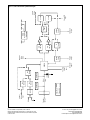
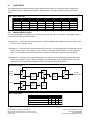
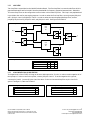
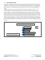
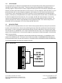
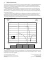
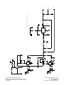
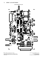
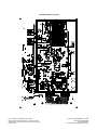
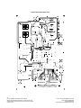
Q0420
PHASE-LOCKED
OSCILLATOR (PLO)
EVALUATION SYSTEM
USER’S GUIDE
INTRODUCTION
The Q0420 PLO Evaluation System is a complete evaluation board designed on a compact 5” x 7.5” printed circuit
card for the Q3236 PLL. The evaluation platform includes a fixed demonstration as well as a custom prototyping
design. A block diagram of the Q0420 is shown in Figure 1. The Q0420 demonstration platform consists of a
phase-locked oscillator system which generates frequencies from 2 GHz to 3 GHz with a minimum step size of 5
MHz over the full output frequency range (÷ 2 prescaler included on-board). The custom prototyping option
allows the designer to rapidly configure a custom synthesizer by adding a VCO, loop filter and reference
suppression filter components to the alternative circuit sections of the board. The user can easily select between
the demonstration platform and the custom prototyping design via on-board jumper options. Additional input and
output connectors are also provided to easily support the use of off-board VCO’s and prescalers to quickly evaluate
the performance tradeoffs between alternative components.
The Q0420 can be computer controlled for remote operation, or alternatively controlled through the on-board
frequency control switches for stand-alone operation. Remote operation is accomplished through the custom
software program, Data I/O Card, and cabling provided with the Q0420 board. The menu-driven software will
automatically compute all desired frequency programming and can exercise the following Q3236 modes of
operation:
• 16-bit Direct Parallel Control
• 8-bit Data Ping-Pong Control
• 8-bit Data Bus Control
• 20-bit Serial Ping-Pong Control
• 20-bit Serial Control
Stand-alone operation with the Q0420 requires only a single +15VDC power supply, but can only utilize the
Q3236’s direct parallel interface for frequency programming using on-board DIP switches.
This User’s Guide provides all the information needed to use the Q0420 PLO Evaluation System. Appendices
are also provided which contain the Q0420 schematics, layout and a complete parts list. When designing custom
synthesizers using the Q0420, it is recommended that the designer also read QUALCOMM’s Q3236 Technical
Data Sheet. It contains numerous design hints and discusses not only the electrical performance of the Q3236,
but also has an application section that discusses how a PLL synthesizer can be designed.
The Q0420 PLO Evaluation System is meant to be a demonstration circuit and evaluation tool. QUALCOMM
does not make any warranty as to the Q0420’s suitability for a specific application without further design
modifications. However, we believe you will find the Q0420 a useful system to further your understanding of
synthesizer design with QUALCOMM’s integrated PLL devices.
CONTENTS
1.0
3.3
GETTING STARTED ......................................... 3
Digital I/O Board Installation .................... 3
3.3.1 Reference Divider .......................... 18
1.2
Digital I/O Board Software
3.3.2 VCO Divider .................................. 18
Configuration .............................................. 3
1.3
Q0420 PLO Evaluation System Software
4.0
1.4
DESCRIPTION OF BOARD FEATURES ......... 20
4.1
Installation .................................................. 5
2.0
DIP Switch Settings .................................. 17
1.1
Q3236 Phase-Locked Loop Frequency
Synthesizer ................................................ 20
Q0420 PLO Evaluation System Setup ....... 6
4.2
Reference Oscillator ................................. 20
SYNTHESIZER OPERATION ............................ 6
4.3
Line Receiver ............................................ 20
2.1
Inputs .......................................................... 6
4.4
Voltage Controlled Oscillator (VCO) ...... 20
2.1.1 Power Supply Requirements .......... 6
4.5
Loop Filter ................................................. 20
2.1.2 External Reference Input; (J1) ......... 6
4.6
Reference Suppression Filter .................... 21
2.1.3 External VCO Input; (J10) ............... 7
4.7
Prescaler .................................................... 21
2.1.4 Ping Pong Control In; (J10) ............. 7
2.2
Outputs ....................................................... 7
5.0
2.2.1 Synthesizer Out; (J9) ....................... 7
2.2.2 Ref. Div. Out; (J2) ............................ 7
2.2.3 VCO Div. Out; (J7) .......................... 7
2.2.4 Prescaler Out; (J8) ............................ 7
2.2.5 Ext. VCO Control; (J5) .................... 7
2.3
Jumper Settings ........................................... 8
2.3.1 Reference Frequency Jumpers ........ 8
2.3.2 Loop Filters ...................................... 9
2.3.3 Op Amp Negative Rail Voltage
Selection .......................................... 9
2.3.4 Reference Suppression Filter ........ 10
2.3.5 VCO Selection ............................... 10
DESIGN HINTS AND SUGGESTIONS .......... 22
5.1
Power Supplies .......................................... 22
5.2
External Reference Source ....................... 22
5.3
Q0420 EMI Shield ..................................... 22
5.4
Phase Offset Trimpot ............................... 22
6.0
RELATED LITERATURE ................................. 22
7.0
APPENDIX ......................................................... 23
7.1
Appendix A: Q0420 Schematic
Drawings ................................................... 24
7.2
Appendix B: Q0420 Parts List .................. 30
7.3
Appendix C: Q0420 layout Drawings ...... 32
QUALCOMM ASIC PRODUCTS ............................. 36
2.3.6 Prescaler ......................................... 12
2.3.7 Q3036 Mode .................................. 12
2.3.8 Ping Pong Mode External
Control ........................................... 12
2.3.9 Test Points ..................................... 12
3.0
Q0420 FREQUENCY CONTROL .................... 13
3.1
Direct Parallel Mode, Eight Bit Bus Mode,
Serial Mode ............................................... 14
3.1.1 Reference Frequency ..................... 14
3.1.2 Output Frequency ......................... 15
3.1.3 Phase Detector Frequency ............ 15
3.1.4 Divide by Two Prescaler ............... 15
3.1.5 PRE EN/ ......................................... 15
3.1.6 Quit ................................................ 15
3.2
Ping Pong Mode ........................................ 16
3.2.1 Output Frequency ......................... 17
2
QUALCOMM Incorporated, ASIC Products
6455 Lusk Boulevard, San Diego, CA 92121-2779, USA
Q0420 Phase-Locked Oscillator (PLO) Evaluation System
User’s Guide
E-mail: [email protected]
Telephone: (619) 658-5005
Fax: (619) 658-1556
Data Subject to ChangeWithout Notice
1.0
GETTING STARTED
The Q0420 PLO Evaluation System requires the following computer hardware as a minimum to operate in
Remote Mode:
• PC 80386 or better
• 4 MB RAM
• Math Coprocessor
• Hard Drive
• Mouse
• Windows™ Version 3.1 or better
• SVGA Video Card (1024 X 768 resolution, small fonts)
The Q0420 PLO Evaluation System consists of a Q0420 Evaluation Board, Q0420 Shield, Q0420 Control Software,
Control Cable, Digital I/O (DIO) Board, and DIO Board Installation Software. In order to operate the Q0420
Evaluation Board in Remote Mode, the DIO Board needs to be installed in a PC. The DIO Driver Software and the
Q0420 Control Software needs to be installed on the hard drive of the PC. To use the Q0420 in Stand-alone Mode,
a PC is not required.
Note: Windows™ is a trademark of Microsoft® Corporation.
1.1
DIGITAL I/O BOARD INSTALLATION
Install the DIO Board in any open slot in your PC according to the CIO-DIO24 User’s Manual provided with the
evaluation system. We recommend the base address of the CIO-DIO be set to 300H and the interrupt level set in
the “X” position.
Once the DIO Board is installed in your PC, the board needs to be configured with the Instacal software
provided. Place the Instacal disk in your floppy drive, access the floppy drive (usually A:) and type “Install”. This
can be accomplished in DOS or Windows.
1.
The Computer Boards Software Installation title screen will appear once the Install.exe file is run. From this
menu select “I”, Install, to proceed and complete installation.
2.
Once the PCMCIA installation window appears, select “No”. Likewise, select “No” to the Universal Library
and Labview Driver Installation Window.
3.
Select the drive and directory you want the Instacal program to reside. We suggest using the default, C:\CB.
The software will automatically copy all files from the disk into the specified directory on your hard drive.
4.
Once all files are copied to your hard drive, the software will ask if you would like to have the
AUTOEXEC.BAT file modified automatically, select “Yes”. The program will automatically add C:\CB to
your path.
5.
1.2
After all files have been copied to your hard drive, reboot your computer to complete the installation process.
DIGITAL I/O BOARD SOFTWARE CONFIGURATION
Once the software installation is complete, it is necessary to configure the software to control the Digital I/O
board. The following procedure will configure and test the DIO drivers to ensure that the software is
communicating with the DIO board.
3
QUALCOMM Incorporated, ASIC Products
6455 Lusk Boulevard, San Diego, CA 92121-2779, USA
Q0420 Phase-Locked Oscillator (PLO) Evaluation System
User’s Guide
E-mail: [email protected]
Telephone: (619) 658-5005
Fax: (619) 658-1556
Data Subject to ChangeWithout Notice
QUALCOMM Incorporated, ASIC Products
6455 Lusk Boulevard, San Diego, CA 92121-2779, USA
Q0420 Phase-Locked Oscillator (PLO) Evaluation System
User’s Guide
Computer
Interface
+5V
External
Reference
Input
Optional Path
Default Path
DB37
40 MHz
DIP Switch
Control
Status
Line
Receiver
Line
Receiver
Lock
Detect
DIP Switch
Q3236
VCO Divider
Output
Ping-Pong
Control
Input
Line
Receiver
Prescaler
Output
Resistive
Divider
Reference
Divider
Output
÷2
Prescaler
Loop
Filter #2
Loop
Filter #1
+ 15 V
+ 15 V
Reference
Filter
Synthesizer
Output
Resistive
Divider
Voltage
Conversion and
Conditioning
+5V
VCO #2
VCO #1
External
VCO Control
External VCO
Input
–5V
Figure 1. Q0420 PLO Evaluation System Block Diagram
4
E-mail: [email protected]
Telephone: (619) 658-5005
Fax: (619) 658-1556
Data Subject to ChangeWithout Notice
1.
Once the software installation is complete, run Instacal.exe located in the drive and directory you chose during
installation, most likely C:\CB.
2.
From the Instacal Menu, double click your mouse on the “Install” pull down menu.
3.
Double click your mouse on “Board #0”.
4.
Select “Board type” and choose the “CIO-DIO24”.
5.
Select the base address to match the address you selected via dip switches located on the CIO-DIO24 Board,
most likely 300H.
6.
Select the Interrupt Level to match the interrupt level you selected via the interrupt jumper located on the
CIO-DIO24 Board, most likely none.
7.
After the board is configured, it can be tested. To do this, double click your mouse on the “Test” pull down
menu.
8.
Select “Board #0 = CIO-DIO24”.
WARNING
BEFORE PROCEEDING TO THE NEXT STEP,
REMOVE ALL EXTERNAL CONNECTIONS
TO THE DIO BOARD
9.
Select “Internal Test”, then “yes”.
10. The software will test the DIO Board checking the input and output registers. If the test is successful, you
will receive a message that states “the DIO Board has been found and the registers have been written to and
read back”. This completes the DIO installation process. If you receive an error message, recheck the jumper
settings on the DIO Board and rerun the Instacal program Step 3 of Digital I/O Software Configuration. If you
continue to receive an error message, contact Computer Boards Inc.
11. Exit from the Instacal program.
1.3
Q0420 PLO EVALUATION SYSTEM SOFTWARE INSTALLATION
The following procedure describes the Q0420 Control Software installation process.
1.
Insert the Q0420 Control Software into the floppy drive of your computer.
2.
Access the floppy drive using the Windows file manager.
3.
Double click your mouse on “Setup.exe”.
5
QUALCOMM Incorporated, ASIC Products
6455 Lusk Boulevard, San Diego, CA 92121-2779, USA
Q0420 Phase-Locked Oscillator (PLO) Evaluation System
User’s Guide
E-mail: [email protected]
Telephone: (619) 658-5005
Fax: (619) 658-1556
Data Subject to ChangeWithout Notice
4.
The software will ask you where you want the files to be installed on your hard drive. The default is:
C:\QUALCOMM\Q0420. The software will require approximately 3 MB of hard drive space. Select “Ok” to
proceed. The software will copy and decompress all files onto your hard drive into the directory you selected.
5.
Once all files have been written to your hard drive, the software will ask you if you want it to automatically
create a Windows program group. The default program group name is “QUALCOMM”. If you select
“Create”, the software will automatically create a program group and a program item for the Q0420 Control
Software. If you select “skip”, the software will not create the program group and program item.
6.
This completes the Q0420 Control Software installation process. Select “Ok”.
1.4
Q0420 PLO EVALUATION SYSTEM SETUP
First, turn off the computer; connecting the Q0420 Control Cable while the PC is on may damage the PC.
Connect the DIO Board located in the PC to the Q0420 Evaluation Board through the DB37 Control Cable
provided. Turn on PC and run Windows.
Before running the Q0420 Evaluation Board Software, ensure the dip switches S1 and S2 are set to the “off” or
logical zero position. Operating the software while the dip switches are in the “1” or high position may damage
the DIO Board. Execute the Q0420 Control Software from the QUALCOMM program group in Windows.
2.0
SYNTHESIZER OPERATION
Figure 1 shows the Q0420 PLO Evaluation System block diagram. The following paragraphs describe the function
and operation of each of the circuit elements shown in the block diagram.
2.1
INPUTS
2.1.1
POWER SUPPLY REQUIREMENTS
A single +15 VDC ± 5% (500 mA capability) power supply is required to operate the Q0420. The +15VDC input is
the red banana jack while ground is the black banana jack. The Q0420 converts and conditions the +15VDC input
to +5VDC. A +15VDC to -5VDC voltage converter circuit is provided on the board for applications that require a
negative rail be supplied to the op amp. The -5V regulation is a switching device and may cause spurious
components on the output of the synthesizer. The -5V circuit is disabled when the board is shipped. Proper
voltage input and conversion is indicated by the three yellow LED’s, DS1-DS3.
2.1.2
EXTERNAL REFERENCE INPUT; (J1)
The External Reference Input allows the user to bypass the on-board 40 MHz reference oscillator. This input can
be used to characterize the synthesizer output when using other reference sources. When the External Reference
Input is used, the reference signal can be selected to be processed by the input line receiver or the reference signal
can bypass the line receiver. Figure 2 illustrates the proper way to connect the on-board jumpers for various
operating modes for the reference inputs. The nominal input to J1 is 0 to 100 MHz, -10 to +5 dBm for a 50 ohm
source. If you choose to use an external reference, the power to the 40 MHz on-board reference should be disabled
to minimize on-board oscillations.
6
QUALCOMM Incorporated, ASIC Products
6455 Lusk Boulevard, San Diego, CA 92121-2779, USA
Q0420 Phase-Locked Oscillator (PLO) Evaluation System
User’s Guide
E-mail: [email protected]
Telephone: (619) 658-5005
Fax: (619) 658-1556
Data Subject to ChangeWithout Notice
2.1.3
EXTERNAL VCO INPUT; (J10)
The External VCO Input is provided as a means to input a signal directly into the differential VCO inputs to the
Q3236. This is necessary when using an external VCO or for troubleshooting the synthesizer system. The
nominal input to J10 is -10 dBm to +3 dBm.
2.1.4
PING PONG CONTROL IN; (J10)
The Ping Pong Control Input is only used when operating the Q3236 in the Ping Pong Mode. The input is routed
to either FSELS or FSELP depending on the jumper position of JP16 and resistors R87 and R88. This input allows
an external CMOS compatible input to switch between the data in the primary registers and the secondary
registers. When FSELS/FSELP is high, the synthesizer output frequency is obtained from the frequency word
stored in the primary registers. Conversely, when FSELS/FSELP is low, the synthesizer output frequency is
obtained from the frequency stored in the secondary registers. This input is ideal for creating a FSK modulator for
slow data rates.
2.2
OUTPUTS
2.2.1
SYNTHESIZER OUT; (J9)
The Synthesizer Out signal provides the 2000 - 3000 MHz output in 5.0 MHz steps when using the on-board
40 MHz reference and VCO. The output power ranges from 0 to +7 dBm.
2.2.2
REF. DIV. OUT; (J2)
The Ref. Div. Out provides a test point to view the divided Input Reference signal to the Phase/Frequency
Detector on the Q3236. This output can also be used along with the VCO Div. Out to drive an external Phase/
Frequency detector or other external circuitry, if desired. Refer to the Q3236 Technical Data Sheet for nominal
output levels.
2.2.3
VCO DIV. OUT; (J7)
The VCO Div. Out provides a test point to view the divided VCO input signal that is being input to the Phase/
Frequency Detector. This output can also be used along with Ref. Div. Out to drive an external Phase/Frequency
detector or other external circuitry, if desired. Refer to the Q3236 Technical Data Sheet for nominal output levels.
2.2.4
PRESCALER OUT; (J8)
The Prescaler Out provides a test point to view the VCO divide-by-two prescaler output signal, which is also
routed to the Q3236 VCO input. The output power of this signal is -25 dBm ± 3 dBm.
2.2.5
EXT. VCO CONTROL; (J5)
The Ext. VCO Control is provided for use with an external VCO. The Ext. VCO Control provides the tuning
voltage to the external VCO. The external VCO output can be fed back to the PLL device via Ext. VCO Input. By
using an external VCO, the Q0420 can generate frequencies from L-Band to Ku-Band or higher. When output
frequencies exceed 3000 MHz, an external prescaler is necessary prior to the Ext. VCO Input.
7
QUALCOMM Incorporated, ASIC Products
6455 Lusk Boulevard, San Diego, CA 92121-2779, USA
Q0420 Phase-Locked Oscillator (PLO) Evaluation System
User’s Guide
E-mail: [email protected]
Telephone: (619) 658-5005
Fax: (619) 658-1556
Data Subject to ChangeWithout Notice
2.3
JUMPER SETTINGS
The Q0420 Evaluation Board has several jumpers which allow the option of choosing multiple configurations.
The evaluation board is shipped with jumpers in default positions. The default jumper positions are listed in
Table 1.
Table 1. Default Jumper Positions
2.3.1
JUMPER
POSITION
JUMPER
POSITION
JUMPER
POSITION
JUMPER
POSITION
JP1
JP2
JP3
JP4
1 and 2
2 and 3
2 and 3
1 and 2
JP5
JP6
JP7
JP8
1 and 2
1 and 2
2 and 3
2 and 3
JP9
JP10
JP11
JP12
1 and 2
1 and 2
1 and 2
1 and 2
JP13
JP14
JP15
JP16
2 and 3
1 and 2
1 and 2
1 and 2
REFERENCE FREQUENCY JUMPERS
There are three possible configurations for the reference jumpers, see Figure 2 and Table 2. We suggest using the
line receiver for frequencies under 40 MHz.
Configuration 1: Use the 40 MHz on-board reference. Use the supplied bi-pin jumpers and connect JP6 pin 1 and
2, JP2 pin 2 and 3, JP8 pin 2 and 3.
Configuration 2: Use the Ext. Ref. Input and select the line receiver. Use the supplied bi-pin jumpers and connect
JP1 pin 2 and 3, JP2 pin 1 and 2, JP8 pin 2 and 3. When not using the on-board reference, connect JP16 pin 2
and 3. This will power-down the on-board 40 MHz reference and decrease extraneous signal generation.
Configuration 3: Use the Ext. Ref. Input and bypass the line receivers. Use the supplied bi-jumpers and connect
JP1 pin 1 and 2, JP8 pin 1 and 2. When not using the on-board reference, connect JP6 pin 2 and 3. This will
power-down the on-board 40 MHz reference and decrease extraneous signal generation.
Figure 2. Reference Jumpers
JP2
External
Reference
Input
1
1
2
3
Line
Receiver
1
2
2
Line
Receiver
3
3
JP1
+5 VDC
To Q3236
Reference Input
JP8
1
2
3
40 MHz
Reference
Line
Receiver
JP6
Table 2. Reference Selection
REFERENCE SELECTION
JP6
On Board Reference
External Reference with Line Receiver
External Reference without Line Receiver
1,2
2,3
2,3
JP1
–
2,3
1,2
JP2
JP8
2,3
1,2
–
2,3
2,3
1,2
8
QUALCOMM Incorporated, ASIC Products
6455 Lusk Boulevard, San Diego, CA 92121-2779, USA
Q0420 Phase-Locked Oscillator (PLO) Evaluation System
User’s Guide
E-mail: [email protected]
Telephone: (619) 658-5005
Fax: (619) 658-1556
Data Subject to ChangeWithout Notice
2.3.2
LOOP FILTERS
Two loop filters are provided on the Q0420 Evaluation Board. The first loop filter is a second order filter which is
populated and optimized for 100 kHz closed loop bandwidth for frequency operation between 2000 - 3000 MHz.
The second loop filter can be configured as a second order or third order loop filter. This loop is not populated and
is provided to the user for prototyping purposes. In order to select the first loop filter, connect jumpers JP10 pin 1
and 2, JP11 pin 1 and 2, and JP14 pin 1 and 2. In order to select the second unpopulated loop filter, connect
jumpers JP10 pin 2 and 3, JP11 pin 2 and 3, and JP14 pin 2 and 3. See Figure 3 and Table 3.
Figure 3. Loop Filter Selection Jumpers
Loop
Filter
#1
1
2
PD_D
-5V
1
3
2
3
VT
3
JP13
1
JP14
2
PD_U
1
2
JP10
Loop
Filter
#2
3
JP11
-5V
1
2
3
JP3
Table 3. Loop Filter Select
LOOP FILTER SELECT
Loop #1
Loop #2
2.3.3
JP10 JP11 JP14
1,2
2,3
1,2
2,3
1,2
2,3
OP AMP NEGATIVE RAIL VOLTAGE SELECTION
The negative rail of the LT1357 OP Amp can be set to either ground or -5 volts. In order to set the negative rail of
the op amp to -5 volts on the first loop filter, connect JP13 pins 1 and 2. To set the negative rail to ground,
connect pins 2 and 3. Connect JP3 pins 1 and 2 to select -5 volts on the second loop filter or pins 2 and 3 for
ground. See Figure 3, Table 4 and Table 5.
Table 4. Negative OP Amp Rail Selection Loop #1
Table 5. Negative OP Amp Rail Selection Loop #2
NEGATIVE RAIL SELECTION LOOP #1
JP13
NEGATIVE RAIL SELECTION LOOP #2
JP3
-5V
GND
1,2
2,3
-5V
GND
1,2
2,3
9
QUALCOMM Incorporated, ASIC Products
6455 Lusk Boulevard, San Diego, CA 92121-2779, USA
Q0420 Phase-Locked Oscillator (PLO) Evaluation System
User’s Guide
E-mail: [email protected]
Telephone: (619) 658-5005
Fax: (619) 658-1556
Data Subject to ChangeWithout Notice
2.3.4
REFERENCE SUPPRESSION FILTER
A reference suppression filter is provided on the board to attenuate the phase/frequency detector error pulses at
the rate FPD. The reference suppression filter was optimized for 2.5 MHz and may need to be redesigned for
different phase detector frequencies. In order to use the reference suppression filter, connect JP15 pins 1 and 2,
and JP4 pins 1 and 2. If the user does not want to utilize the filter, connect JP15 pins 2 and 3, and JP4 pins 2 and 3.
See Figure 4 and Table 6.
Figure 4. Reference Suppression Filter Jumpers
Table 6. Reference Filter Select
Reference
Suppression
Filter
1
VT
REFERENCE FILTER SELECT JP15 JP4
2
VCO VT
2
3
1,2
2,3
3
JP15
2.3.5
1,2
2,3
IN
Bypass
1
JP4
VCO SELECTION
The evaluation board can accommodate two VCO’s or utilize an external VCO. The board is shipped with a
2000 -3000 MHz VCO, U7, already installed. The user can install a different VCO, U8, or route the tune voltage
off the evaluation board to an external VCO. Once the VCO is properly installed, the voltage tune path and the
VCO output path needs to be configured. Figure 5, Table 7 and Table 8 show the VCO voltage tune paths and the
VCO RF output paths.
Figure 5. VCO Selection Jumpers
+ 5V + 15V
R30
0
JP9
R31
0
1
VCO
Power
Conditioning
PWR
VT
VCO
#1
2
3
U7
1
VT VCO
2
R23
0Ω
R69
0Ω
R86
0Ω
U8
3
R82
0Ω
PWR VCO
VT
#2
JP5
VCO
OUT
External VCO
Input
External VCO
Control
Table 7. VCO Select
Table 8. VCO Power
VCO SELECT
JP5
R23
R69
R86
R82
VCO #1
VCO #2
External VCO
1,2
2,3
Open
OUT
OUT
IN
IN
OUT
OUT
OUT
OUT
IN
OUT
IN
OUT
VCO POWER
+5V
+ 15 V
VCO #1
VCO #2
R30
R31
IN
OUT
–
–
OUT
IN
–
–
JP9
–
–
1,2
2,3
10
QUALCOMM Incorporated, ASIC Products
6455 Lusk Boulevard, San Diego, CA 92121-2779, USA
Q0420 Phase-Locked Oscillator (PLO) Evaluation System
User’s Guide
E-mail: [email protected]
Telephone: (619) 658-5005
Fax: (619) 658-1556
Data Subject to ChangeWithout Notice
Configuration 1: Default VCO, U7. Connect JP5 pins 1 and 2 to route the tune voltage to the default VCO. R23,
the zero ohm resistor, should be removed for optimum performance. Install R69, a zero ohm resistor, and
remove R82 and R86 to select the correct RF output path.
Configuration 2: Second VCO, U8. Connect JP5 pins 2 and 3 to route the tune voltage to the second VCO, U8.
R23, the zero ohm resistor, should be removed for optimum performance. Install R82, a zero ohm resistor,
and remove R69 and R86 to select the correct RF output path. Also, an AC coupling capacitor, C95, needs to
be installed. This capacitor is not provided. The capacitor value selected should be optimized for the
frequency output of the VCO.
Configuration 3: External VCO. Remove the jumper on JP6 and install a zero ohm resistor in R23 to route the
tune voltage to an external VCO. The external VCO tune voltage will be present on J5, a BNC connector.
Install R86, a zero ohm resistor, and remove R69 and R82. Also, an AC coupling capacitor, C94, needs to be
installed. This capacitor is not provided. The capacitor value selected should be optimized for the frequency
output of the VCO.
Fifteen volts or five volts can be routed to the power pin of either VCO depending on the operating voltage of the
user’s VCO. Installing R31, a zero Ohm resistor, routes +15 volts to jumper J9. When R30 is installed, +5V is
routed to J9. See Table 8. CAUTION: R30 and R31 cannot be installed at the same time. Damage may occur to
the board if this happens.
As stated above, the Q0420 can accommodate two VCO’s. Each VCO pad can accept two types of VCO
footprints, either a standard 0.81” square pin-type package or a standard 0.91” square surface mount package. In
order to accommodate the two VCO footprints, the tune voltage, supply voltage and VCO output are routed
through 0Ω resistors. The Q0420 is manufactured with the resistors configured for the pin-type VCO’s. If the user
would like to use a surface mount VCO footprint, the 0Ω resistors need to be configured according to
Figure 6.
Figure 6. VCO Pad Configuration
VCO Supply
Voltage
VCO Supply
Voltage
VCO Tune
Voltage
VCO Tune
Voltage
R39
R62
VT
R38
R63
VT
+V
R66
VT
U7
U7
VCO #1
Pin-Type
Footprint
R41
VCO #1
Surface Mount
Footprint
R40
VT
U8
VCO #2
Pin-Type
Footprint
+V
R67
U8
+V
VCO #2
Surface Mount
Footprint
VCO Output
VCO Output
VCO Output
VCO Output
R60
R61
R64
R65
VCO Output
+V
VCO Output
11
QUALCOMM Incorporated, ASIC Products
6455 Lusk Boulevard, San Diego, CA 92121-2779, USA
Q0420 Phase-Locked Oscillator (PLO) Evaluation System
User’s Guide
E-mail: [email protected]
Telephone: (619) 658-5005
Fax: (619) 658-1556
Data Subject to ChangeWithout Notice
2.3.6
PRESCALER
A divide-by-two prescaler is provided in the VCO feedback path on the evaluation board as shown in Figure 7 and
Table 9. This allows the Q3236 to synthesize frequencies above 2.0 GHz. The prescaler can be used in the
feedback path to the Q3236 or it can be bypassed. Install zero ohm resistors in R78 and R75, and remove resistors
R85 and R84 to utilize the prescaler. In order to bypass the prescaler, remove resistors R78 and R75, and install
zero ohm resistors in R85 and R84.
Figure 7. Prescaler Select Jumpers
R78
0Ω
R75
0Ω
÷2
Prescaler
R85
0Ω
R84
0Ω
Table 9. Prescaler Select
÷2 PRESCALER SELECT R78
R75
R85
R84
MODE SELECT JUMPERS
JP7 Connection
IN
OUT
IN
OUT
OUT
IN
OUT
IN
Enhanced Mode (Access to M7, M8, R4, R5)
Q3036 Mode/
Pins 1 and 2
Pins 2 and 3
IN
Bypass
2.3.7
Table 10. Mode Select
Q3036 MODE
The Q3236 is pin-for-pin compatible with the Q3036 PLL and can be used as a direct replacement. Pin 44 of the
Q3236 must be pulled “low” to operate in the Q3036 mode. Connect pins 2 and 3 of JP7 to pull pin 44 “low”. To
use the Q3236 in Normal Mode and have access to the upper M and A counter bits, connect JP7 pins 1 and 2,
which pulls pin 44 “high”, see Table 10.
2.3.8
PING PONG MODE EXTERNAL CONTROL
When operating the Q0420 in Ping Pong Mode, the output frequency register selected can be controlled either
through the control software or through the external Ping Pong Control In, Connector J6. If you are using the
software to control which frequency register is selected, then the Q0420 does not need to be modified. To use the
External Ping Pong Control Input to control frequency selection, then board modifications are required. If using
Eight Bit Bus Ping Pong Mode, connect pins 2 and 3 of J16 and remove R88. This will route the input on J6 to the
FSELP pin on the Q3236 and will disable the software from controlling the FSELP pin. If using Serial Bus Ping
Pong Mode, connect pins 1 and 2 of JP16 and remove R87. This will route the input of J6 to the FSELS pin on the
Q3236 and will disable the software from controlling the FSELS pin.
2.3.9
TEST POINTS
Test points are located throughout the evaluation board for your convenience during testing and evaluation. Refer
to the schematic in Appendix A for test points.
12
QUALCOMM Incorporated, ASIC Products
6455 Lusk Boulevard, San Diego, CA 92121-2779, USA
Q0420 Phase-Locked Oscillator (PLO) Evaluation System
User’s Guide
E-mail: [email protected]
Telephone: (619) 658-5005
Fax: (619) 658-1556
Data Subject to ChangeWithout Notice
3.0
Q0420 FREQUENCY CONTROL
The frequency of the Q0420 can either be controlled through software and the Digital I/O Board or by setting the
DIP Switches. The software that is provided with the Q0420 Evaluation Board allows the user to program the
Q3236 in each of the five programming modes: Direct Parallel, Eight Bit Bus, Serial Bus, Ping Pong Eight Bit Bus,
Ping Pong Serial Bus. The control software calculates the value of the M,A, and R counters and programs the
Q3236.
Before executing the Q0420 Control Software, make sure all DIP switches S1 and S2 are set to “0”. From
Windows, double click on the Q0420 Control Software icon to execute the software. The window shown in
Figure 8 will appear. If this window or subsequent windows do not fit on your monitor, then your video driver
needs to be changed. For optimum performance, choose a video driver that supports a resolution of 1024 by 768
and at least 256 colors. You may move or resize the window as required. Choose the method in which you want
to program the Q3236 by selecting the programming method and then selecting the execute button. One of five
programming windows will appear. The window for Direct Parallel Mode, Eight Bit Bus Mode, and Serial Mode
look the same but the programming of the Q3236 is carried out differently. Likewise, the Ping Pong Eight Bit Bus
Mode and the Ping Pong Serial Mode front panels look the same but the programming of the Q3236 is carried out
differently.
Figure 8. Programming Mode Selection Software Screen
Programming Mode Selection
Direct Parallel Mode
Execute
Eight Bit Bus Mode
Serial Bus Mode
Ping Pong, Eight Bit Bus Mode
QUALCOMM Q0420 EVALUATION
BOARD SOFTWARE VER. 1.0
Ping Pong, Serial Bus Mode
13
QUALCOMM Incorporated, ASIC Products
6455 Lusk Boulevard, San Diego, CA 92121-2779, USA
Q0420 Phase-Locked Oscillator (PLO) Evaluation System
User’s Guide
E-mail: [email protected]
Telephone: (619) 658-5005
Fax: (619) 658-1556
Data Subject to ChangeWithout Notice
3.1
DIRECT PARALLEL MODE, EIGHT BIT BUS MODE, SERIAL MODE
When either Direct Parallel Mode, Eight Bit Bus Mode, or Serial Bus Mode is selected from the Programming Mode
Selection Menu (Figure 8), the window shown in Figure 9 will appear. The software will ask you if you want to go
through the jumper setting windows. If you are a first time user of the evaluation board, it is suggested that you
go through the jumper setting windows. You may also choose to bypass the jumper setting windows.
The programming window shown in Figure 9 represents a block diagram of a phase-locked loop. The user has
control of the Reference Frequency, Output Frequency, Phase Detector Frequency, Divide-by-Two Prescaler, PRE
EN/ and QUIT. The Reference Divide, VCO Divide, R Value, M Value, A Value, R is not an Integer, R out of
Range, and N is not an Integer are calculated from the inputs selected by the user. These values are then
programmed into the Q3236 automatically. The lock detect LED monitors pin 43 of the Q3236 and indicates if
the synthesizer is locked.
Figure 9. Q0420 Front Panel Software Screen
Q3236
Reference
Frequency (MHz)
VCO
Ref.
Divide
40
16
PRE EN/
Phase
Loop
Detector
Filter
Output Frequency (MHz)
3000.000
R is not an Integer
2.50
(MHz)
Lock Detect
Enable
Disable
VCO
Divide
R out of Range
Divide
by 2
Prescalar
600
R Value
IN
15
OUT
N is not an Integer
M out of Range
M Value
A Value
59
QUIT
0
Output Frequency Selection
1000 MHz
100 MHz
10 MHz
1 MHz
4
10
10
10
3
8
8
8
6
6
6
4
4
4
2
2
2
0
0
0
0
3
0
0
0
2
1
kHz
0.00
QUALCOMM Q0420 EVALUATION BOARD
SOFTWARE VER. 1.0
3.1.1
REFERENCE FREQUENCY
The reference frequency can be changed to match the frequency being supplied to the Q3236. The Q0420 Board is
supplied with a 40 MHz reference crystal oscillator; therefore, the default is set to 40 MHz. Changing this icon
does not change the frequency supplied to the Q3236; it only aids in calculating the R value. If the value of R is
14
QUALCOMM Incorporated, ASIC Products
6455 Lusk Boulevard, San Diego, CA 92121-2779, USA
Q0420 Phase-Locked Oscillator (PLO) Evaluation System
User’s Guide
E-mail: [email protected]
Telephone: (619) 658-5005
Fax: (619) 658-1556
Data Subject to ChangeWithout Notice
not an integer based on the reference frequency and the frequency of the phase detector, (R=Reference/FPD -1), the
R is not an Integer LED will illuminate red. Conversely, if the value of R is an integer, the LED will illuminate
green. If the value of R exceeds the number of R counter bits, the R Out of Range LED will illuminate red. If the
value of R is in range, the LED will illuminate green. The R Out of Range Condition is calculated differently
depending on the programming mode. Refer to the Q3236 Specifications for the different ranges of R.
3.1.2
OUTPUT FREQUENCY
The output frequency of the VCO is selected from the four slides and the number of kHz selected. The sum of the
slides is displayed next to the VCO block. The slides can be changed to move the VCO in course steps or fine
steps. The resultant VCO divide value is shown in the VCO Divide Block. The N is Not an Integer LED will
illuminate red if the VCO divide value is not an integer based upon the desired output frequency, the frequency of
the phase detector, (N=VCO Frequency/Frequency of the Phase Detector), the state of the Divide-by-Two Prescaler
Switch, and PRE EN/. If N is an integer, the LED will illuminate green. The M and A values are calculated based
upon the value of the VCO Divide and are displayed below the block diagram. The software calculates if M is
within range of the M counter bits available, depending on the programming mode. If M is within range, the M in
Range LED will illuminate green; if M is out of range, the LED will be red. The Q0420 Evaluation Board was
designed to generate output frequencies from 2.0 to 3.0 GHz in 5 MHz steps.
3.1.3
PHASE DETECTOR FREQUENCY
The phase detector frequency, synthesizer step size, is chosen from the control located under the Phase Detector
Frequency block of the block diagram. The phase detector frequency can be as large as 100 MHz or small as
desired as long as the values of R and M are within range. The Q0420 Evaluation Board was designed with a
default value of 2.5 MHz phase detector frequency.
3.1.4
DIVIDE-BY-TWO PRESCALER
An external divide-by-two prescaler is provided on the evaluation board for output frequency operation up to 3.0
GHz. If using the prescaler in the output frequency feedback path, the switch should be placed in the “IN”
position. The software automatically calculates the M and A values based upon the divide-by-two prescaler in the
feedback path. If not using the prescaler in the feedback path, the position should be switched to the “OUT”
position. When the prescaler is not used, the maximum frequency of the PLL is 2.0 GHz.
3.1.5
PRE EN/
The PRE EN/ switch selects the internal mode of operation of the Q3236. When the PRE EN/ is enabled, the PRE
EN/ value is “low” or zero volts. In this mode, frequency division is accomplished with a pulse-swallow counter
made up of the 10/11 front-end dual modulus prescaler. In this mode, frequency division up to 3.0 GHz on the
Q0420 Evaluation Board is possible.
When the PRE EN/ switch is disabled, the Q3236 internal prescaler is bypassed so that the VCO input
frequency is divided by the M counter and the A counter is ignored. The M counter operates at frequencies up to
300 MHz. In this mode, frequency division ratios are continuous from 1 to 511.
3.1.6
QUIT
When the Quit button is selected, the current programming mode is exited and the Programming Mode Selection
Window is displayed.
15
QUALCOMM Incorporated, ASIC Products
6455 Lusk Boulevard, San Diego, CA 92121-2779, USA
Q0420 Phase-Locked Oscillator (PLO) Evaluation System
User’s Guide
E-mail: [email protected]
Telephone: (619) 658-5005
Fax: (619) 658-1556
Data Subject to ChangeWithout Notice
3.2
PING PONG MODE
When either Ping Pong Eight Bit Bus Mode or Ping Pong Serial Bus Mode is selected from the Programming Mode
Selection Menu (Figure 8) the window shown in Figure 10 will appear. The software will ask you if you want to go
through the jumper setting windows. If you are a first time user of the evaluation board, it is suggested that you
go through the jumper setting windows. You may also choose to bypass the jumper setting windows.
The programming window shown in Figure 10 represents a block diagram of a phase-locked loop. The user has
control of the Reference Frequency, Output Frequency, Phase Detector Frequency, Divide-by-Two Prescaler,
PRE EN/ and QUIT. The Reference Divide, VCO Divide, R Value, M Value, A Value, R is not an integer, R out of
range, and N is not an integer is calculated from the inputs selected by the user. The lock detect LED monitors
pin 43 of the Q3236 and indicates if the synthesizer is locked.
All control features are the same as previously described, except for the output frequency control.
Figure 10. Ping Pong Mode Front Panel Software Screen
Reference
Frequency (MHz)
40
Q3236
16
PRE EN/
2500 Frequency 2 (MHz)
VCO
Ref.
Divide
Phase
Loop
Detector
Filter
Frequency Select
R is not an Integer
2.50
(MHz)
Lock Detect
2400 Frequency 1 (MHz)
Enable
Disable
VCO
Divide
R out of Range
Divide
by 2
Prescalar
600
R Value
IN
15
M out of Range
OUT
N is not an Integer
M Value
A Value
59
0
QUIT
QUALCOMM Q0420 EVALUATION BOARD
SOFTWARE VER. 1.0
16
QUALCOMM Incorporated, ASIC Products
6455 Lusk Boulevard, San Diego, CA 92121-2779, USA
Q0420 Phase-Locked Oscillator (PLO) Evaluation System
User’s Guide
E-mail: [email protected]
Telephone: (619) 658-5005
Fax: (619) 658-1556
Data Subject to ChangeWithout Notice
3.2.1
OUTPUT FREQUENCY
In Ping Pong Mode, two frequencies are programmed on the front panel (Figure 10) and the output frequency is
selected from the Frequency Select Switch. These two frequencies are programmed in Q3236 primary and
secondary registers. When the switch is down, the phase-locked loop will lock at the frequency displayed in the
Frequency One box and the associated values of VCO Divide, M, and A are displayed. When the switch is up, the
phase-locked loop will lock at the frequency displayed in the Frequency Two box and the associated values of
VCO Divide, M, and A are displayed. If the VCO Divide value is not an integer based upon the desired output
frequency, the frequency of the phase detector, the state of the Divide-by-Two Prescaler Switch, and PRE EN/, the
N is Not an Integer LED will illuminate red. If N is an integer, the LED will illuminate green. The M and A
values are calculated based upon the value of the VCO Divide and are displayed below the block diagram. The
software calculates if M is within range, depending on the programming mode. If M is within range, the M in
Range LED will illuminate green; if M is out of range, the LED will be red.
3.3
DIP SWITCH SETTINGS
The Q0420 can also be operated without the control software and programmed directly through the dip switches
located on the evaluation board. Remove the Q0420 Programming Cable before operating the board through the
DIP switches. In order to operate the Q0420 Evaluation Board in Direct Parallel Mode, connect JP7 pins 2 and 3.
This will pull pin 44, /Q3036 Mode, “low” and pin 22, Busmode/ will float “high”, thus configuring the Q3236 to
operate in Direct Parallel Mode. In this mode, the upper M counter bits M7, M8 and the upper R counter bits R4
and R5 are not available.
The Q0420 has two DIP style 8-position switches (S1 and S2) that provide the R, M, A and PRE EN/ control
inputs to the Q3236 (Figure 11). The inputs control the division moduli for the REFERENCE (R0-R3) and VCO
Dividers (M0-M6 and A0-A3) as well as the selection of the PRESCALER or NONPRESCALER Modes (PRE EN/).
The following paragraphs describe how to program S1 and S2.
Figure 11. DIP Switch Control
A3
A2
A1
A0
EN/
M6
M5
M4
M3
M2
M1
M0
R3
R2
R1
R0
1
8
16
8
Q3236
PHASE-LOCKED
LOOP
FREQUENCY
SYNTHESIZER
0
17
QUALCOMM Incorporated, ASIC Products
6455 Lusk Boulevard, San Diego, CA 92121-2779, USA
Q0420 Phase-Locked Oscillator (PLO) Evaluation System
User’s Guide
E-mail: [email protected]
Telephone: (619) 658-5005
Fax: (619) 658-1556
Data Subject to ChangeWithout Notice
3.3.1
REFERENCE DIVIDER
The QUALCOMM Q3236 has an on-chip Reference Divider. The divider is a 4-bit counter and will divide the
reference input by 1-16 in unit steps; this corresponds to the Q3236 functioning in “Q3036 Mode” (Refer to
Q3236 Technical Data Sheet). For the Reference Divider to divide the 40 MHz reference to 2.50 MHz, it must be
programmed with a divide ratio of 16. The procedure for computing the binary values of R0, R1, R2 and R3 are as
follows:
R = (FREF + FPD) - 1
R = (FREF + FPD) - 1 = (40 MHz ÷ 2.5 MHz) - 1 = 15 (decimal) = 1111 (binary)
R0, R1, R2, R3 = high (switches “1”)
3.3.2
VCO DIVIDER
When using the Prescaler Mode, the VCO Divider has the capability of dividing the VCO input by values ranging
from 90-1295 in unit steps. For the Q0420 to synthesize the output frequency range of 2000 MHz to 3000 MHz
using the FPD of 2.50 MHz, the VCO Divider must be programmed through the moduli range of 400 to 600. The
Q0420 provides a ÷2 prescaler in the VCO frequency feed back path to the Q3236, which allows the Q3236 to
synthesize frequencies greater than 2000 MHz. The ÷2 prescaler divides the VCO output frequency by two, thus
the Q3236 only sees frequencies from 1000 MHz to 1500 MHz. The following section describes the procedure for
programming the M and A control inputs to the QUALCOMM PLLFS.
To program the Q0420 PLO Evaluation System to output FVCO = 2500 MHz, the total divide ratio is:
N = FVCO ÷ FPD ÷ External Prescaler = 2500 MHz ÷ 2.5 MHz ÷ 2 = 500.
The binary values for M and A are computed as follows:
M = Integer {N÷10} - 1 = Integer {500 ÷ 10} - 1 = 49 decimal = 0110001 binary
M0, M4, M5 = high (switches “1”)
M1, M2, M3, M6 = low (switches “0”)
A = N - {10(M+1)} = 500 - {10(49 + 1)} = 0 decimal = 0000 binary
A0-A3 = low (switches “0”)
Since the output frequency of the synthesizer board is above 300 MHz, the VCO Divider is programmed to the
Prescaler Mode which is selected by setting PRE EN/ to low (switches “0”).
The above information is then used to program S1 and S2. S1 and S2 are programmed by setting the respective
switch to the “0” position to set the control input to a low and to the “1” position to set the control input to a
high.
To program the Q0420 PLO Evaluation System to output FVCO = 2000 MHz, the total divide ratio is:
N = FVCO ÷ FPD ÷ Prescaler = 2000 MHz ÷ 2.5 ÷ 2 = 400
M = Integer {N ÷ 10} - 1 = Integer {400 ÷ 10} - 1 = 39 decimal = 0100111 binary
M0, M1, M2, M5 = high (switch “1”)
M3, M4, M6 = low (switch “0”)
A = N - {10(M + 1)} = 400 - {10(39 + 1)} = 0 decimal = 0000 binary
A0, A1, A2, A3 = low (switch “0”)
18
QUALCOMM Incorporated, ASIC Products
6455 Lusk Boulevard, San Diego, CA 92121-2779, USA
Q0420 Phase-Locked Oscillator (PLO) Evaluation System
User’s Guide
E-mail: [email protected]
Telephone: (619) 658-5005
Fax: (619) 658-1556
Data Subject to ChangeWithout Notice
This same procedure can be followed to program the Q0420 PLO Evaluation System to output any frequency in
the range of 2000 - 3000 MHz in 5.0 MHz steps. Table 11 shows the correct switch settings in 100 MHz
increments.
Table 11. Output Frequency Switches
Synthesizer
Output Freq. (J1)
2000 MHz
Ref. Divider
R Counter
R0 = 1
R1 = 1
R2 = 1
R3 = 1
2100 MHz
R0 = 1
R1 = 1
R2 = 1
R3 = 1
2200 MHz
R0 = 1
R1 = 1
R2 = 1
R3 = 1
2300 MHz
R0 = 1
R1 = 1
R2 = 1
R3 = 1
2400 MHz
R0 = 1
R1 = 1
R2 = 1
R3 = 1
2500 MHz
R0 = 1
R1 = 1
R2 = 1
R3 = 1
VCO
M Counter
M0 = 1
M1 = 1
M2 = 1
M3 = 0
M4 = 0
M5 = 1
M6 = 0
M0 = 1
M1 = 0
M2 = 0
M3 = 1
M4 = 0
M5 = 1
M6 = 0
M0 = 1
M1 = 1
M2 = 0
M3 = 1
M4 = 0
M5 = 1
M6 = 0
M0 = 1
M1 = 0
M2 = 1
M3 = 1
M4 = 0
M5 = 1
M6 = 0
M0 = 1
M1 = 1
M2 = 1
M3 = 1
M4 = 0
M5 = 1
M6 = 0
M0 = 1
M1 = 0
M2 = 0
M3 = 0
M4 = 1
M5 = 1
M6 = 0
Ref. Divider
R Counter
R0 = 1
R1 = 1
R2 = 1
R3 = 1
Divider
A Counter
A0 = 0
A1 = 0
A2 = 0
A3 = 0
Synthesizer
Output Freq. (J1)
A0 = 0
A1 = 0
A2 = 0
A3 = 0
2700 MHz
R0 = 1
R1 = 1
R2 = 1
R3 = 1
A0 = 0
A1 = 0
A2 = 0
A3 = 0
2800 MHz
R0 = 1
R1 = 1
R2 = 1
R3 = 1
A0 = 0
A1 = 0
A2 = 0
A3 = 0
2900 MHz
R0 = 1
R1 = 1
R2 = 1
R3 = 1
A0 = 0
A1 = 0
A2 = 0
A3 = 0
3000 MHz
R0 = 1
R1 = 1
R2 = 1
R3 = 1
2600 MHz
VCO
M Counter
M0 = 1
M1 = 1
M2 = 0
M3 = 0
M4 = 1
M5 = 1
M6 = 0
M0 = 1
M1 = 0
M2 = 1
M3 = 0
M4 = 1
M5 = 1
M6 = 0
M0 = 1
M1 = 1
M2 = 1
M3 = 0
M4 = 1
M5 = 1
M6 = 0
M0 = 1
M1 = 0
M2 = 0
M3 = 1
M4 = 1
M5 = 1
M6 = 0
M0 = 1
M1 = 1
M2 = 0
M3 = 1
M4 = 1
M5 = 1
M6 = 0
Divider
A Counter
A0 = 0
A1 = 0
A2 = 0
A3 = 0
A0 = 0
A1 = 0
A2 = 0
A3 = 0
A0 = 0
A1 = 0
A2 = 0
A3 = 0
A0 = 0
A1 = 0
A2 = 0
A3 = 0
A0 = 0
A1 = 0
A2 = 0
A3 = 0
A0 = 0
A1 = 0
A2 = 0
A3 = 0
19
QUALCOMM Incorporated, ASIC Products
6455 Lusk Boulevard, San Diego, CA 92121-2779, USA
Q0420 Phase-Locked Oscillator (PLO) Evaluation System
User’s Guide
E-mail: [email protected]
Telephone: (619) 658-5005
Fax: (619) 658-1556
Data Subject to ChangeWithout Notice
4.0
DESCRIPTION OF BOARD FEATURES
4.1
Q3236 PHASE-LOCKED LOOP FREQUENCY SYNTHESIZER
Please refer to the Q3236 Technical Data Sheet for details and features of this integrated PLL device.
4.2
REFERENCE OSCILLATOR
The Q0420’s on-board reference is a 40 MHz oscillator with ECL-level output. This oscillator was selected for its
excellent short-term noise performance. The device does not have temperature compensation for long-term
frequency drift. It is recommended that when performing phase noise measurements on the Q0420 PLO
Evaluation System, a stable low noise external reference be used. The output from an HP8662B Signal Generator
(back panel reference) provides an excellent 10 MHz reference for performing phase noise measurements.
4.3
LINE RECEIVER
In most synthesizer applications, phase noise performance is invariably a driving design requirement. The VCO
and Reference Dividers are edge-triggered circuits. Random jitter on the input clock edges results in phase noise
in the synthesizer output spectrum. Additive AM noise on the input reference signal can cause random jitter.
The Reference Divider’s sensitivity to this jitter can be decreased by ensuring that the input clock passes through
the zero crossing threshold transition zone as quickly as possible. The line receiver performs this function by
squaring up the edges of the input reference signal. We recommend using the on-board line receiver for input
frequencies below 40 MHz if the input reference does not already have squared transitions.
4.4
VOLTAGE CONTROLLED OSCILLATOR (VCO)
The Q0420 can accommodate two VCOs simultaneously. One VCO used on the Q0420 Evaluation Board has KV =
95 MHz/V and a tuning range of 2000 - 3000 MHz. This high performance VCO helps demonstrate the low phase
noise performance of PLO synthesizer systems designed around the QUALCOMM PLL device. The second VCO
footprint is left unpopulated. Each VCO footprint accepts a pin-type or surface mount device.
4.5
LOOP FILTER
The differential phase detector outputs of the Q3236 are input to an active loop filter. The loop filter type is a
modified loop filter with a pre-integrator. The loop filter was designed with a closed loop bandwidth of 100 kHz
and a damping constant of 0.9. The values of the loop filter components were computed using the equations found
in the Q3236 Technical Data Sheet. Appendix A lists component values.
Figure 12. Reference Suppression Filter
From
Loop
Filter
C53
270 pF
C24
330 pF
L5
15 µH
L4
15 µH
C51
470pF
C54
1500pF
C52
1500pF
To
VCO
Tune
20
QUALCOMM Incorporated, ASIC Products
6455 Lusk Boulevard, San Diego, CA 92121-2779, USA
Q0420 Phase-Locked Oscillator (PLO) Evaluation System
User’s Guide
E-mail: [email protected]
Telephone: (619) 658-5005
Fax: (619) 658-1556
Data Subject to ChangeWithout Notice
4.6
REFERENCE SUPPRESSION FILTER
The purpose of the Reference Suppression Filter is to attenuate undesired signals. A flip-flop type phase/frequency
detector produces error pulses at FPD. These pulses modulate the VCO and produce sidebands at FPD and at
harmonics of FPD. The Reference Suppression Filter is typically a low pass filter with fast transition times from
passband to stopband (i.e., Elliptic Topology).
The Reference Suppression Filter designed for the Q0420 PLO Evaluation System is a five pole elliptical low
pass filter. See Figure 12. The filter was designed to provide a wide “notch” at FPD = 2.5 MHz, the Q0420 phase
detector frequency. This design results in more than 70 dBc reference suppression for frequencies greater than 2.5
MHz, as seen in Figure 13.
Utilizing the five pole reference suppression filter, sideband spurs are suppressed to acceptable levels but the
phase margin of the loop is also degraded. The Reference Suppression Filter on the Q0420 Evaluation Board
degrades the phase margin by 12.5° at 100 kHz. Phase margin can be increased by designing narrower loop filters
or by using a 3 pole elliptical filter. See the Q3236 Technical Data Sheet.
Figure 13. Reference Suppression Filter Graph
Phase
(Degrees)
Amplitude
(dBc)
+20
180
0
1
– 20
0
1
– 40
3
– 60
S21
P21
2
– 80
10 kHz
100 kHz
AMPLITUDE
PHASE
4.7
100 kHZ (Marker 1)
– .02
– 12.5661
– 180
1 MHz
2.5 MHZ (Marker 2)
– 76.8
–
10 MHz
5.0 MHZ (Marker 3)
– 43.2
–
PRESCALER
The Q0420 provides a divide-by-2 prescaler in the feedback path. This allows frequencies greater than 2.0 GHz to
be synthesized using the Q3236. This prescaler operates up to 3.0 GHz. With the installation of two 0 Ω resistors,
the prescaler can be utilized or bypassed.
21
QUALCOMM Incorporated, ASIC Products
6455 Lusk Boulevard, San Diego, CA 92121-2779, USA
Q0420 Phase-Locked Oscillator (PLO) Evaluation System
User’s Guide
E-mail: [email protected]
Telephone: (619) 658-5005
Fax: (619) 658-1556
Data Subject to ChangeWithout Notice
5.0
DESIGN HINTS AND SUGGESTIONS
5.1
POWER SUPPLIES
Passive filtering of the power supply inputs is provided on-board the Q0420. For optimal synthesizer performance,
it is recommended that a clean voltage supply be used to supply power to the PLL device to eliminate any
contributions of extraneous noise coupling through the power bus lines to the synthesizer’s output.
5.2
EXTERNAL REFERENCE SOURCE
The external reference input is provided to enable you to use a PLL reference of your choice. This feature is
important when performing low noise measurements or to have a reference source other than the on-board
40 MHz reference.
5.3
Q0420 EMI SHIELD
The Q0420 Evaluation Board comes complete with an EMI Circuit Card Assembly Shield. This shield was
designed to reduce the effect of RF-coupling to the Q0420 PLO Evaluation System from typical lab RF emissions.
5.4
PHASE OFFSET TRIMPOT
The Phase/Frequency Detector of the Q3236 is “linearized”, i.e., there is no dead zone, due to the addition of a
residual pulse onto both phase detector outputs. This situation can be exploited by a phase offset adjust circuit to
optimize the comon-mode rejection of the phase detector output pulses as they are subtracted from one another in
the differential active loop filter. The Q0420 introduces this phase offset by using the method described on page
37 of the Q3236 Technical Data Sheet. A trimpot (R51) is used to bias the phase detector outputs. The phase
offset allows you to trade off between reference spurs and phase noise. The optimum phase offset allows the phase
detector output (PD U OUT or PD D OUT) to reach its full amplitude. Typically a phase offset of 10 ns is
sufficient and also allows for mismatches in temperature coefficients of the differential active loop filter.
6.0
RELATED LITERATURE
Q3236 2.0 GHz Low Power PLL Frequency Synthesizer Technical Data Sheet
Hybrid PLL/DDS Frequency Synthesizers, AN2334-4
22
QUALCOMM Incorporated, ASIC Products
6455 Lusk Boulevard, San Diego, CA 92121-2779, USA
Q0420 Phase-Locked Oscillator (PLO) Evaluation System
User’s Guide
E-mail: [email protected]
Telephone: (619) 658-5005
Fax: (619) 658-1556
Data Subject to ChangeWithout Notice
7.0
APPENDIX
23
QUALCOMM Incorporated, ASIC Products
6455 Lusk Boulevard, San Diego, CA 92121-2779, USA
Q0420 Phase-Locked Oscillator (PLO) Evaluation System
User’s Guide
E-mail: [email protected]
Telephone: (619) 658-5005
Fax: (619) 658-1556
Data Subject to ChangeWithout Notice
7.1
APPENDIX A: Q0420 SCHEMATIC DRAWINGS
J4
.
J1
BNC
+15V_IN
EXT_REF_IN
J3
.
GND
P1
DB37M
1
2
3
4
5
6
7
8
9
10
11
12
13
14
15
16
17
18
19
20
21
22
23
24
25
26
27
28
29
30
31
32
33
34
35
36
37
SMODE_A3
M2_WR_A2
A1
FSELP_A0
FSELS_DBUS7_PRE/
SCLK_DBUS6_M6
SDATA_DBUS5_M5
SEN/_DBUS4_M4
J2
BNC
REF_DIV_OUT
J7
BNC
VCO_DIV_OUT
J9
SMA
SYNTH_OUT
LOCK_DETECT
HOP_WR
A_WR
M1_WR
BUSMODE/
DBUS3_M3
DBUS2_M2
DBUS1_M1
DBUS0_M0
R_3
R_2
R_1
R_0
J8
SMA
PRESCALER_OUT
J5
BNC
J6
BNC
EXT_VCO_CONTROL
PING_PONG_CNTRL
J10
SMA
EXT_VCO_IN
24
QUALCOMM Incorporated, ASIC Products
6455 Lusk Boulevard, San Diego, CA 92121-2779, USA
Q0420 Phase-Locked Oscillator (PLO) Evaluation System
User’s Guide
E-mail: [email protected]
Telephone: (619) 658-5005
Fax: (619) 658-1556
Data Subject to ChangeWithout Notice
A1
VCO_IN/
VCO_IN
BUSMODE/
M1_WR
A_WR
HOP_WR
SMODE_A3
M2_WR_A2
FSELP_A0
R88 0
.
FSELS_DBUS7_PRE/
JP16 1
2
PING_PONG_CNTRL
3
R870
C74
100PF
C80
100PF
C75
100PF
C32
100PF
C79
100PF
C81
100PF
C31
100PF
C78
100PF
C29
100PF
C30
100PF
SPST8
C77
100PF
C76
100PF
C56
1000PF
C57
1000PF
C58
1000PF
C59
1000PF
C25
1000PF
C26
1000PF
C27
1000PF
C28
1000PF
17 VEE1
C84
68PF
C88
68PF
R71
100
16 PRE_EN
15 M6
14 M5
13 M4
12 VCC2
11 VCC1
10 M3
9 M2
8 M1
7 M0
VEE0
SPST8
SEN/_DBUS4_M4
SDATA_DBUS5_M5
SCLK_DBUS6_M6
C60
0.1UF
+5V
C61
1000PF
2
3
A0
18
16
15
14
13
12
11
10
9
R90
10K
8
7
6
5
1
R3IN
A1
19
1
2
3
4
5
6
7
8
R89
10K
1
2
3
4
+5V
R2IN
A2
20
16
15
14
13
12
11
10
9
C38
100PF
8
7
6
5
R70
RNET4S
10K
JP7
R1IN
A3
21
1
2
3
4
5
6
7
8
LOCK_DETECT
REF
1
2
3
4
R45
RNET4S
10K
6
ROIN
BUSMODE
22
8
7
6
5
5
VCC0
VCC3
23
8
7
6
5
1
2
3
4
4
Q3036
M1WR
24
R56
RNET4S
10K
3
25
R_0
R_1
R_2
R_3
DBUS0_M0
DBUS1_M1
DBUS2_M2
DBUS3_M3
1
2
3
4
S2
2
43
LDOUT
AWR
R36
RNET4S
10K
.
26
S1
1
42
RFIN
HOPWR
+5V
44
41
RFIN
VCOIN
27
+5V
40
VCOIN
28
+5V
.
.
1
2
C39
1000PF
3
DS4
C83
1000PF
+5V
VEE2 29
VDIV 30
VCCO0 31
N/C 32
VCC4 33
CEXT 34
VCC5 35
PU 36
PD 37
C82
0.1UF
CD90_24083_1
U9
C42
0.1UF
750
RDIV 39
R37
270
+15V
R42
VCCO1 38
VEE3
QUALCOMM Incorporated, ASIC Products
6455 Lusk Boulevard, San Diego, CA 92121-2779, USA
Q0420 Phase-Locked Oscillator (PLO) Evaluation System
User’s Guide
E-mail: [email protected]
Telephone: (619) 658-5005
Fax: (619) 658-1556
Data Subject to ChangeWithout Notice
25
R59
1K
C44
0.1UF
+5V
VCO_DIV_OUT
C62
0.1UF
R55
33K
R53
DNI
+5V
REF_DIV_OUT
PD_D
PD_U
L6
33UH
R43
1K
C65
1000PF
C63
1000PF
C64
0.1UF
+5V
C40
0.1UF
+5V
C66
0.1UF
26
QUALCOMM Incorporated, ASIC Products
6455 Lusk Boulevard, San Diego, CA 92121-2779, USA
Q0420 Phase-Locked Oscillator (PLO) Evaluation System
User’s Guide
E-mail: [email protected]
Telephone: (619) 658-5005
Fax: (619) 658-1556
Data Subject to ChangeWithout Notice
PD_U
PD_D
CCW
W CW
R51
500
R49
1K
TP5
TP4
R50
1K
1
1
+15V
3
JP111
2
3
JP101
2
R54
39
R35
DNI
R33
DNI
C47
10UF
R32
39
R52
150
C50
DNI
R21
DNI
R18
DNI
C48
0.1UF
C70
3300PF
R48
150
C67
3300PF
C45
DNI
+15V
R44
150
R46
150
+
C23
DNI
R20
DNI
7
4
+
2 -
3
R19
DNI
C20
DNI
R47
665
C68
.01UF
4
2 -
3
7
R34
DNI
C46
DNI
2
3
JP13
1
C49
DNI
6
R22
DNI
U6
LT1357CN8
6
2
3
1
C72
10UF
1
JP3
1
R28
100
TP1
U10
LT1357CN8 R58
100
C22
10UF
C69
0.1UF
-5V
2
-5V
3
1
C21
0.1UF
JP14
2
3
1
JP15
F2F1F0 G
C51
470PF
1
3
C53
270PF
.L5
15UH
6
TP6
4
R57
665
2
5
C71
.01UF
F2F1F0 G
C54
1500PF
1
3
1
2
JP4
3
C24
330PF
.L4
15UH
6
C87
0.1UF
4
C73
10UF
2
5
3
EXT_VCO_CONTROL
VT2
JP5
VT1
1
R23
DNI
2
C52
1500PF
1
TP3
1
D3
MMBD914X
VT2
.
.
.
R39
0
R38
DNI
R40
DNI
R41
0
EXT_VCO_IN
D2
MMBD914X
VT1
TP2
JP9
3
4
RFO
RFO
VCC
1
R86
DNI
R61
DNI
R60
0
R65
DNI
R64
0
R67
DNI
C98
0.1UF
C99
1000PF
U8
DNI
.
R66
0
C94
DNI
1
R63
DNI
C95
DNI
R82
DNI
R81
16
R69
0
C93
4.7PF
C97
0.1UF
C96
1000PF
+5V
+15V
U7
.
R62
0
VCC
TV
3 TV
3
G4
1
G1
2
G0
2
C55
1.0UF
Q3
.
MMBT2222AL
R30
DNI
R31
0
6dB
R80
16
6dB
R79
16
R85
DNI
R78
0
R77
16
6dB
R68
68
R76
16
C92
4.7PF
+5V
JP12
NC1 5
NC0 1
RFO0 6
RFO1 7
U11
U832BS_AFP
C86
0.1UF
.
C89
39PF
C90
39PF
R75
0
R84
DNI
-15dB
R74
8.2
WHEN U832 IS NOT IN USE
R83
75
R73
120
VCO_IN
SYNTH_OUT
PRESCALER_OUT
3dB
R72
8.2
ADDED JUMPER TO PREVENT OSCILLATION
+2.5dBm MAX INPUT
-9dBm MIN INPUT
C91
4.7PF
3 RFI1
2 RFI0
C85
1000PF
L7
33UH
1
R29
100
8
3
G3
G2
G3
G2
7
6
G4
4
8
7
6
5
G1
5
G0
2
2
8
V
GND
4
QUALCOMM Incorporated, ASIC Products
6455 Lusk Boulevard, San Diego, CA 92121-2779, USA
Q0420 Phase-Locked Oscillator (PLO) Evaluation System
User’s Guide
E-mail: [email protected]
Telephone: (619) 658-5005
Fax: (619) 658-1556
Data Subject to ChangeWithout Notice
27
28
QUALCOMM Incorporated, ASIC Products
6455 Lusk Boulevard, San Diego, CA 92121-2779, USA
Q0420 Phase-Locked Oscillator (PLO) Evaluation System
User’s Guide
E-mail: [email protected]
Telephone: (619) 658-5005
Fax: (619) 658-1556
Data Subject to ChangeWithout Notice
3
.
1 JP6
2
+5V
EXT_REF_IN
C43
10UF
.
2
3
4
GND
VCC
U5
40MHZ 2
C19
.01UF
JP1
1
9
1
U4
C18
0.1UF
U4
R24
510
12 10
4
R25
510
2 20 MC10H115FN
3
2 20 MC10H115FN
12 10
8
C34
.01UF
+5V
C33
.01UF
5
7
3
R27
51
C37
0.1UF
R26
51
C35
0.1UF
+5V
3
.
1 JP2
2
C17
1000PF
13
14
12 10
12 10
18
2 20 MC10H115FN
U4
+5V
19
R17
510
U4
2 20 MC10H115FN
C36
.01UF
17
15
UNUSED PART
+5V
3
1
.
JP8
2
REF
C41
0.1UF
QUALCOMM Incorporated, ASIC Products
6455 Lusk Boulevard, San Diego, CA 92121-2779, USA
Q0420 Phase-Locked Oscillator (PLO) Evaluation System
User’s Guide
E-mail: [email protected]
Telephone: (619) 658-5005
Fax: (619) 658-1556
Data Subject to ChangeWithout Notice
29
C10
10UF
+15V_IN
U1
LT1054CS8
C5
10UF
L1
33UH
3
GND
VR 6
4 C-
VO 5
OSC 7
2 C+
V+
FB/SD 1
8
C1
10UF
D1
5.1V
R1
DNI
E1
TURRET
E2
TURRET
F1
.
500MA
C9
2200PF
R16
510K
R12
100K
C3
0.1UF
C8
100UF/6V
C4
10UF
.
DS1
LED1Y
R2
1.5K 1/4W
R4
10K
R3
2K
R8
75
Q1
.
MMBT3904
C12
22UF/25V
4
G
R10
DNI
R7
1K
C7
68UF/10V
U3
LT1021DCS8_5
2 IN
OUT 6
C6
33UF
L2
100UH
R14
100
C11
.01UF
C15
100UF/6V
+
4
2 1
8
3
7
L3
33UH
6
U2
LT1007CS8
C13
33UF
C2
0.47UF
DS3
LED3Y.
C16
68UF/10V
R9
1K
C14
100UF/20V
R15
470
10ma
-5V
.
DS2
LED2Y
R11
470
10ma
R13
1
+5V
R6
68/1W
Q2
.
2N2219
R5
68/1W
+15V
7.2
APPENDIX B: Q0420 PARTS LIST
REFERENCE
DESIGNATOR
R31,R39,R41, R60,R62, R64, R66, R69,
R75, R78, R87-R88
R7
R12
R3
R55
R11,R15
R16
R8,R83
R2
R5-R6
R14,R28-R29,R58,R71
R9,R43,R49-R50,R59
R4,R89-R90
R73
R76-R77,R79-R81
R13
R37
R32,R54
R26-R27
R17,R24-R25
R68
R42
R72,R74
R44,R46,R48,R52
R47,R57
R36,R45,R56,R70
R51
C89-C90
C91-C93
C84,C88
C52,C54
C9
C53
C24
C67,C70
C51
C68,C71
C29-C32,38,C74-C81
C25-C28,C56-C59
C17,C39,C61,C63,65C83,C85,C96,C99
C11,C19,C33-C34,C36
C3,C18,C21,C35,C37,C40-C42,C44,C48,
C60,C62,C64,C66,C69,C82,C86-C87,
C97-C98
QUALCOMM MCN
MANUFACTURERS
PART NUMBER
1
25-24109-1
25-24109-1
PWB, Q0420, Eval Board
12
100-01011-0000
RM73Z2B000J
RES, Chip Thick Film Zero 5% 1/8W (Size 1206)
QTY
PART DESCRIPTION
1
1
1
1
2
1
2
1
2
5
5
3
1
5
1
1
2
2
3
1
1
2
4
2
4
1
2
3
2
2
1
1
1
2
1
2
13
8
9
5
100-01011-1001
100-01011-1003
100-01011-2001
100-01011-3302
100-01011-4700
100-01011-5103
100-01011-75R0
100-01011-1501
100-02323-68R0
100-06723-0101
100-06723-0102
100-06723-0103
100-06723-0121
100-06723-0160
100-06723-01R0
100-06723-0271
100-06723-0390
100-06723-0510
100-06723-0511
100-06723-0680
100-06723-0751
100-06723-08R2
100-06725-1500
100-06725-6650
101-08318-0103
102-01023-5000
105-01073-0390
105-01073-04R7
105-01073-0680
105-01073-1152
105-01073-1222
105-01073-1271
105-01073-1331
105-01073-1332
105-01073-1471
105-01073-3103
105-01073-6101
105-01247-6102
105-01247-0102
105-01247-0103
RM73B2B102J
RM73B2B104J
RM73B2B202J
9C12063A333JLR
RM73B2B471J
9C12063A514JLR
9C12063A750JLR
CRCW1210-152J
CRCW2512680J
RM73B2A101J
RM73B2A102J
RM73B2A103J
MCR10JW121
RM73B2A160J
MCR10JW1R0
RM73B2A271J
CRCW0805-390J
RM73B2A510J
RM73B2A511J
RM73B2A680J
RM73B2A751J
MCR10JW8R2
MCR10FX1500
MCR10FX6650
EXBV8V103J
3266W-1-501
C0805C390J5GAC3
C0805C479D1GAC3
C0805C680J5GAC
C1206C152J5GACT
1206C0222J2B04
1206C0271J2B04
1206C0331J2B04
VJ1206A332JXAM
VJ1206A471JXBM
VJ1812A103XAM
VJ0603A101JXAA
C0603C102K5RAC
500R15W0102KW2VJ0805Y103KXBM
RES, Chip Thick Film 1.0K 5% 1/8W +/-200PPM/C
RES, Chip Thick Film 100K 5% 1/8W +/-200PPM/C
RES, Chip Thick Film 2.0K 5% 1/8W +/-200PPM/C
RES, Chip Thick Film 33K 5% 1/8W +/-200PPM/C
RES, Chip Thick Film 470 5% 1/8W +/-200PPM/C
RES, Chip Thick Film 510K 5% 1/8W +/-200PPM/C
RES, Chip Thick Film 75 5% 1/8W +/-200PPM/C
RES, Chip Thick Film 1.5K 5% 1/4W +/-200PPM/C
RES, Chip Thick Film 68 5% 1W +/-200PPM/C
RES, Chip Thick Film 100 5%.1W +/-200PPM/C
RES, Chip Thick Film 1.0K 5%.1W +/-200 PPM/C
RES, Chip Thick Film 10K 5%.1W +/-200 PPM/C
RES, Chip Thick Film 120 5%.1W +/-200 PPM/C
RES, Chip Thick Film 16.0 5%.1W +/-200 PPM/C
RES, Chip Thick Film 1.0 5%.1W +/-200 PPM/C
RES, Chip Thick Film 270 5%.1W +/-200 PPM/C
RES, Chip Thick Film 39.0 5%.1W +/-200 PPM/C
RES, Chip Thick Film 51.0 5%.1W +/-200 PPM/C
RES, Chip Thick Film 510 5%.1W +/-200 PPM/C
RES, Chip Thick Film 68.0 5%.1W +/-200 PPM/C
RES, Chip Thick Film 750 5%.1W +/-200 PPM/C
RES, Chip Thick Film 8.2 5%.1W +/-200 PPM/C
RES, Chip Thick Film 150 1%.1W +/-200 PPM/C
RES, Chip Thick Film 665 1%.1W +/-200 PPM/C
RES Chip Network, 10K 5% 12V 300PPM (4RES) Isolated
RES, Variable 500 10% 1/4W 12 Turn 1/4" Sq
CAP, Chip Ceramic 39PF 5% COG/NPO 50V
CAP, Chip Ceramic 4.7PF +/-.5PF COG/NPO 50V
CAP, Chip Ceramic 68PF 5% COG/NPO 50V
CAP, Chip Ceramic 1500PF 5% COG/NPO 50V
CAP, Chip Ceramic 2200PF 5% COG/NPO 50V
CAP, Chip Ceramic 270PF 5% COG/NPO 50V
CAP, Chip Ceramic 330PF 5% COG/NPO 50V
CAP, Chip Ceramic 3300PF 5% COG/NPO 50V
CAP, Chip Ceramic 470PF 5% COG/NPO 50V
CAP, Chip Ceramic .01U F 5% COG/NPO 50V
CAP, Chip Ceramic 100PF 5% COG/NPO 50V
CAP, Chip Ceramic 1000PF 10% X7R 50V
CAP, Chip Ceramic 1000PF 10% X7R 50V
CAP, Chip Ceramic .01UF 10% X7R 50V
20
105-01249-0104
VJ0805U104MXA
CAP, Chip Ceramic .1UF 20% Z7U 50V
30
QUALCOMM Incorporated, ASIC Products
6455 Lusk Boulevard, San Diego, CA 92121-2779, USA
Q0420 Phase-Locked Oscillator (PLO) Evaluation System
User’s Guide
E-mail: [email protected]
Telephone: (619) 658-5005
Fax: (619) 658-1556
Data Subject to ChangeWithout Notice
REFERENCE
DESIGNATOR
C55
C2
C1,C4-C5,C10,C22,C43,C47,C72-C73
C6,C13
C12
C8,C15
C7,C16
C14
L2
L6-L7
L1,L3
L4-L5
U7
U5
D2-D3
D1
Q3
Q1
Q2
U4
U1
U3
U2
U6,U10
U11
S1-S2
DS1-DS3
DS4
F1
E1-E2
TP1-TP6
JP1-JP16
J4
J3
P1
J8-J10
J1-J2,J5-J7
U9
QTY
QUALCOMM MCN
MANUFACTURERS
PART NUMBER
1
1
9
ALT
2
ALT
1
2
2
1
1
2
2
2
1
1
2
1
1
1
1
1
1
1
1
2
1
2
3
1
1
2
6
16
1
1
1
3
5
1
2
1
1
1
16
105-01249-4105
105-07324-0474
105-07490-0106
105-10035-0106
105-10016-0336
105-10036-0336
106-01067-0226
106-02646-0107
106-02648-0686
106-10018-0101
110-02161-0104
110-02161-0333
110-06324-0330
111-05086-0150
137-06030-3018
137-08473-4000
140-01263-0914
141-01260-05R1
160-01028-2222
160-01028-3904
162-10017-2219
211-02623-0115
281-02268-1003
281-10014-0000
281-10015-0000
281-10019-0000
284-08150-0003
304-01668-0001
310-06441-1001
310-06441-1003
326-07302-0000
446-06598-0000
449-01086-0001
449-01086-0003
470-01902-0001
470-01902-0002
474-02449-0037
480-01064-0057
480-01453-0022
CD90-24083-1
500-01350-0308
500-02488-0044
325-06847-0050
520-01805-0011
448-01403-0000
VJ1825U105MXAM
THCS30E1H474ZT
THCS50E1E106ZT
THCR50E1E106ZT
THCS70E1E336ZT
THCR70E1E336ZT
T491D226K025AS7
T491D107K006AS
T491D686K010AS
CACFM1D101M
IMC-1812-100UH
IMC-1812-33UH+
7130-19
614BN-9150Z
M3500C-2032T
SG-615PH 40.0MH
MMBD0914LT1
PMBZ5231B
MMBT2222
MMBT3904
2N2219A
MC10H115FN
LT1054CS8
LT1021DCS8-5
LT1007CS8
LT1357CN8
U832BS-AFP
78RB08S
LYS260DOE7502
LUS250DOE7502
354 101-GY
160-1558-02-01TSW-101-07-L-S
TSW-103-07-L-S
111-0702-001
111-0703-001
747252-4
85SMA50-0-44
413631-1
CD90-24083-1
SMO-8-S6T
PLCC-44-SMT-TT
AGC-1/2
2226B
MSB-2360-100-AU
PART DESCRIPTION
CAP, Chip Ceramic 1.0 UF 20% Z5U 50V
CAP, Chip Ceramic 0.47UF +80/-20% Y5U 50V
CAP, Chip Ceramic 10UF +80/-20% Y5U 25V
CAP, Chip Ceramic 10UF +80/-20% Y5U 25V
CAP, Chip Ceramic 33UF +80/-20% Y5U 25V
CAP, Chip Ceramic 33UF +80/-20% Y5U 25V
CAP,Chip Tant 22UF 10% 25V
CAP,Chip Tant 100UF 10% 6V
CAP,Chip Tant 68UF 10% 10V
CAP, Solid AL 100 UF +/-20% 20V Hi Freq
Inductor, Chip 100UH 10% Q=50 SRF=8.0MHz
Inductor, Chip 33UH 10% Q=50 SRF=11MHz
Inductor, Mini Choke 33UH 10% High Current
Inductor, VAR Shield 15UH
Oscillator, Voltage Controlled 2000-3200MHz
Oscillator, Crystal 40.0MHz +/-100PPM W/Enable
Diode, Switching General Purpose
Diode, Zener 5.1V 5% 225MW
Transistor, NPN HFE=10V At VCE=10V IC=150MA
Transistor, NPN HFE=10V At VCE=1V IC=10MA
Transistor, General Purpose
IC, 10KH Ecl Quad Line Receiver
IC, Voltage Converter Switched Capacitor W/Reg
IC, Voltage Reference Precision 5.0V +/-20PPM/C
IC, Operational Amp Precision High Speed Low Noise
IC, Operational Amp High Speed High Slew Rate
IC, Prescaler Div By 2 3.0GHz
Switch, Dip SPST 8-Pos Slide Recessed
LED, High-Efficiency Diffused Yellow
LED, High-Efficiency Diffused Red/Green
Fuseholder, PCB MT Single Pole 3AG Fuse
Terminal, Solder Turret Silver .062" PCB
Conn, Strip Header .025SQ 1X1 POS PCB .230 AU/SN
Conn, Strip Header .025SQ 1X3 POS PCB .230 AU/SN
Conn, Banana Plug/Binding Post No Term Red
Conn, Banana Plug/Binding Post No Term Black
Conn, D-Sub R/A PCB Metal Shell 37-POS
Conn, SMA R/A PCB Female Receptacle
Conn, BNC Jack R/A PC Mount 500HM
IC, PLL2, Frequency Synthesizer, Com'l
Socket, IC 8-Pin .3MIL PCB Mach. Screw AU Contact
Socket, IC PLCC 44-Pin SMT Low-Profile No POL-PEG
Fuse, N America 1/2A 1/4X1-1/4 Fast/No Delay
Heatsink, TO-5 D=.75" Press-On
Jumper, Terminal Bi-Pin
31
QUALCOMM Incorporated, ASIC Products
6455 Lusk Boulevard, San Diego, CA 92121-2779, USA
Q0420 Phase-Locked Oscillator (PLO) Evaluation System
User’s Guide
E-mail: [email protected]
Telephone: (619) 658-5005
Fax: (619) 658-1556
Data Subject to ChangeWithout Notice
7.3
APPENDIX C: Q0420 LAYOUT DRAWINGS
Q0420 Evaluation Board "Top Silk"
32
QUALCOMM Incorporated, ASIC Products
6455 Lusk Boulevard, San Diego, CA 92121-2779, USA
Q0420 Phase-Locked Oscillator (PLO) Evaluation System
User’s Guide
E-mail: [email protected]
Telephone: (619) 658-5005
Fax: (619) 658-1556
Data Subject to ChangeWithout Notice
Q0420 Evaluation Board "Top Traces"
33
QUALCOMM Incorporated, ASIC Products
6455 Lusk Boulevard, San Diego, CA 92121-2779, USA
Q0420 Phase-Locked Oscillator (PLO) Evaluation System
User’s Guide
E-mail: [email protected]
Telephone: (619) 658-5005
Fax: (619) 658-1556
Data Subject to ChangeWithout Notice
Q0420 Evaluation Board "Bottom Traces"
34
QUALCOMM Incorporated, ASIC Products
6455 Lusk Boulevard, San Diego, CA 92121-2779, USA
Q0420 Phase-Locked Oscillator (PLO) Evaluation System
User’s Guide
E-mail: [email protected]
Telephone: (619) 658-5005
Fax: (619) 658-1556
Data Subject to ChangeWithout Notice
35
QUALCOMM Incorporated, ASIC Products
6455 Lusk Boulevard, San Diego, CA 92121-2779, USA
Q0420 Phase-Locked Oscillator (PLO) Evaluation System
User’s Guide
E-mail: [email protected]
Telephone: (619) 658-5005
Fax: (619) 658-1556
Data Subject to ChangeWithout Notice
QUALCOMM ASIC PRODUCTS
DESCRIPTION
PRODUCT #
NAME
Q2368
Q2240
Q2334
Q2220
Q3236
Q0310
Q0320
Q0420
Q0710
Q0256
Q1650
Q1875
Q4413
Q4401
Q0810
Q0820
Q5500
Q5505
Q5270
Q5312
Q5160
Dual Direct Digital Synthesizer (DDS)
Direct Digital Synthesizer (DDS)
Dual Direct Digital Synthesizer (DDS)
Direct Digital Synthesizer (DDS)
Phase-Locked Loop (PLL) Frequency Synthesizer
DDS Evaluation Board
DDS Evaluation Board
PLO Evaluation System
DDS-Driven PLL Frequency Synthesizer
Viterbi Decoder
Viterbi Decoder
Trellis Codec
Vocoder
Vocoder
Vocoder Evaluation Board
Vocoder Evaluation System
Receive Automatic Gain Control Amplifier
Transmit Automatic Gain Control Amplifier
Mobile Station Modem (MSM2.2)
Analog Baseband Processor (BBA2)
Cell Site Modem (CSM)
130 MHz / 65 MHz
100 MHz
50 MHz / 20 MHz
50 MHz
2.0 GHz
Evaluation of Q2334
Evaluation of Q2220
Evaluation of Q3236
Evaluation of Q2334 & Q3236
256 kbps
25 Mbps, 10 Mbps, 2.5 Mbps
75 Mbps, 30 Mbps
13.3 kbps
8 kbps
Evaluation of Q4401
Evaluation of Q4401
300 MHz
300 MHz
For CDMA Subscriber Unit
For CDMA Subscriber Unit
For CDMA Base Station
• Data books, application notes and user’s guides are available for detailed design information.
Q0420 Phase-Locked Oscillator (PLO) Evaluation System User’s Guide
Data Subject to Change Without Notice
For customer service or technical assistance, please contact:
QUALCOMM Incorporated, ASIC Products
6455 Lusk Boulevard, San Diego, CA 92121-2779, USA
E-mail: [email protected]
Telephone: (619) 658-5005
Fax: (619) 658-1556
80-24112-1
7/96


![2 Clique no botão [OK].](http://vs1.manualzilla.com/store/data/006043970_1-e2974f1cd0f0465d2cb4d13e53c48ce2-150x150.png)