1
CIO-EXP-BRIDGE16
User’s Manual
Revision 2
January, 2001
© Copyright 2001, OMEGA ENGINEERING INC.
Table of Contents
1 INTRODUCTION . . . . . . . . . . . . . . . . . . . . . . . . . . . . . . . . . . . . . . . . . . . . . . . . . . . . . . . . . . . . . . 1
2 SOFTWARE INSTALLATION . . . . . . . . . . . . . . . . . . . . . . . . . . . . . . . . . . . . . . . . . . . . . . . . . . 1
3 GENERAL CONFIGURATION . . . . . . . . . . . . . . . . . . . . . . . . . . . . . . . . . . . . . . . . . . . . . . . . . . 2
3.1 A/D Board Type Select Jumper . . . . . . . . . . . . . . . . . . . . . . . . . . . . . . . . . . . . . . . . . . . . . . . 2
3.2 Setting The Output Channel . . . . . . . . . . . . . . . . . . . . . . . . . . . . . . . . . . . . . . . . . . . . . . . . . 2
3.3 Configuring the A/D Board . . . . . . . . . . . . . . . . . . . . . . . . . . . . . . . . . . . . . . . . . . . . . . . . . . 3
3.3.1 DAS08 Family Setup . . . . . . . . . . . . . . . . . . . . . . . . . . . . . . . . . . . . . . . . . . . . . . . . . . . . . 3
3.3.2 DAS16 Family Setup . . . . . . . . . . . . . . . . . . . . . . . . . . . . . . . . . . . . . . . . . . . . . . . . . . . . . 3
3.3.3 All A/D Boards . . . . . . . . . . . . . . . . . . . . . . . . . . . . . . . . . . . . . . . . . . . . . . . . . . . . . . . . . . 3
3.4 CONNECTING THE CIO-EXP-BRIDGE16 TO THE A/D BOARD . . . . . . . . . . . . . 4
3.4.1 Connecting to a DAS08 Series A/D Board . . . . . . . . . . . . . . . . . . . . . . . . . . . . . . . . . . . 4
3.4.2 Connecting to a DAS16 Series A/D Board . . . . . . . . . . . . . . . . . . . . . . . . . . . . . . . . . . . 4
3.4.3 Other A/D Boards . . . . . . . . . . . . . . . . . . . . . . . . . . . . . . . . . . . . . . . . . . . . . . . . . . . . . . . . 4
3.5 Powering The CIO-EXP-BRIDGE16 . . . . . . . . . . . . . . . . . . . . . . . . . . . . . . . . . . . . . . . . . . 4
3.5.1 Power Source Switch . . . . . . . . . . . . . . . . . . . . . . . . . . . . . . . . . . . . . . . . . . . . . . . . . . . . . 5
3.5.2 Powering with the 37-pin Connector . . . . . . . . . . . . . . . . . . . . . . . . . . . . . . . . . . . . . . . . 5
3.5.3 Powering with the Molex Connector . . . . . . . . . . . . . . . . . . . . . . . . . . . . . . . . . . . . . . . . 5
3.5.4 Powering Through the Power Screw Terminals . . . . . . . . . . . . . . . . . . . . . . . . . . . . . . . 5
3.6 Daisy-Chaining CIO-EXP-BRIDGE16 Boards . . . . . . . . . . . . . . . . . . . . . . . . . . . . . . . . . 6
3.7 Connecting a Test Voltage . . . . . . . . . . . . . . . . . . . . . . . . . . . . . . . . . . . . . . . . . . . . . . . . . . . 6
3.8 Verifying The Installation . . . . . . . . . . . . . . . . . . . . . . . . . . . . . . . . . . . . . . . . . . . . . . . . . . . 6
4 CONFIGURATION FOR VOLTAGE MEASUREMENT . . . . . . . . . . . . . . . . . . . . . . . . . . . 7
4.1 Channel Selection . . . . . . . . . . . . . . . . . . . . . . . . . . . . . . . . . . . . . . . . . . . . . . . . . . . . . . . . . . . 7
4.2 Powering the CIO-EXP-BRIDGE16 . . . . . . . . . . . . . . . . . . . . . . . . . . . . . . . . . . . . . . . . . . 7
4.3 Determining The Appropriate Gain . . . . . . . . . . . . . . . . . . . . . . . . . . . . . . . . . . . . . . . . . . . 7
4.4 Setting the Gain . . . . . . . . . . . . . . . . . . . . . . . . . . . . . . . . . . . . . . . . . . . . . . . . . . . . . . . . . . . . . 8
4.4.1 Setting Board Gain . . . . . . . . . . . . . . . . . . . . . . . . . . . . . . . . . . . . . . . . . . . . . . . . . . . . . . . 8
4.4.2 Setting Channel Gain . . . . . . . . . . . . . . . . . . . . . . . . . . . . . . . . . . . . . . . . . . . . . . . . . . . . . 9
4.5 Attenuation . . . . . . . . . . . . . . . . . . . . . . . . . . . . . . . . . . . . . . . . . . . . . . . . . . . . . . . . . . . . . . . . 10
4.6 Connecting Voltage Signals . . . . . . . . . . . . . . . . . . . . . . . . . . . . . . . . . . . . . . . . . . . . . . . . . 10
4.6.1 Single Ended . . . . . . . . . . . . . . . . . . . . . . . . . . . . . . . . . . . . . . . . . . . . . . . . . . . . . . . . . . . 11
4.6.2 Floating Differential . . . . . . . . . . . . . . . . . . . . . . . . . . . . . . . . . . . . . . . . . . . . . . . . . . . . . 11
4.6.3 Fully Differential . . . . . . . . . . . . . . . . . . . . . . . . . . . . . . . . . . . . . . . . . . . . . . . . . . . . . . . 11
4.7 Verifying the Installation . . . . . . . . . . . . . . . . . . . . . . . . . . . . . . . . . . . . . . . . . . . . . . . . . . . 11
5 CONFIGURATION FOR RESISTANCE MEASUREMENT . . . . . . . . . . . . . . . . . . . . . . 12
5.1 Channel Select . . . . . . . . . . . . . . . . . . . . . . . . . . . . . . . . . . . . . . . . . . . . . . . . . . . . . . . . . . . . . 12
5.2 VEXC Jumper Select . . . . . . . . . . . . . . . . . . . . . . . . . . . . . . . . . . . . . . . . . . . . . . . . . . . . . . . 12
5.3 Powering The CIO-EXP-BRIDGE16 . . . . . . . . . . . . . . . . . . . . . . . . . . . . . . . . . . . . . . . . . 12
5.3.1 Selecting the Power Source for the Board . . . . . . . . . . . . . . . . . . . . . . . . . . . . . . . . . . 12
5.3.2 Selecting the Power Source for the Excitation Voltage . . . . . . . . . . . . . . . . . . . . . . . 12
5.3.3 Selecting the Excitation Voltage . . . . . . . . . . . . . . . . . . . . . . . . . . . . . . . . . . . . . . . . . . 13
5.4 Determining the Appropriate Gain . . . . . . . . . . . . . . . . . . . . . . . . . . . . . . . . . . . . . . . . . . 14
5.5 Setting the Gain . . . . . . . . . . . . . . . . . . . . . . . . . . . . . . . . . . . . . . . . . . . . . . . . . . . . . . . . . . . .
5.5.1 Setting Board Gain . . . . . . . . . . . . . . . . . . . . . . . . . . . . . . . . . . . . . . . . . . . . . . . . . . . . . .
5.5.2 Setting Channel Gain . . . . . . . . . . . . . . . . . . . . . . . . . . . . . . . . . . . . . . . . . . . . . . . . . . . .
5.6 Configuring the Bridge . . . . . . . . . . . . . . . . . . . . . . . . . . . . . . . . . . . . . . . . . . . . . . . . . . . . .
5.6.1 Bridge Completion Resistors . . . . . . . . . . . . . . . . . . . . . . . . . . . . . . . . . . . . . . . . . . . . .
5.6.2 Nulling Potentiometers & Arm Resistor . . . . . . . . . . . . . . . . . . . . . . . . . . . . . . . . . . . .
5.6.3 Strain Gauge Bridge Configuration Examples . . . . . . . . . . . . . . . . . . . . . . . . . . . . . . .
6 SPECIFICATIONS . . . . . . . . . . . . . . . . . . . . . . . . . . . . . . . . . . . . . . . . . . . . . . . . . . . . . . . . . . . .
7 APPENDIX . . . . . . . . . . . . . . . . . . . . . . . . . . . . . . . . . . . . . . . . . . . . . . . . . . . . . . . . . . . . . . . . . . . .
7.1 About Strain Gauges . . . . . . . . . . . . . . . . . . . . . . . . . . . . . . . . . . . . . . . . . . . . . . . . . . . . . . .
7.1.1 What Are Strain Gauges? . . . . . . . . . . . . . . . . . . . . . . . . . . . . . . . . . . . . . . . . . . . . . . . .
7.1.2 Specification of Strain Gauges . . . . . . . . . . . . . . . . . . . . . . . . . . . . . . . . . . . . . . . . . . . .
7.2 Reference Material for Application of Strain Gauges . . . . . . . . . . . . . . . . . . . . . . . . . .
14
14
15
16
16
17
17
21
23
23
23
23
23
1
INTRODUCTION
The CIO-EXP-BRIDGE16 is a signal conditioning accessory designed for use with the DAS08 and
DAS16 family of data acquisition boards. The CIO-EXP-BRIDGE16 contains circuitry to condition
strain gauge sensors on a per channel basis and convert the sensor's output to a voltage suitable for
conversion by a DAS08 or other analog-to-digital conversion board.
This manual is organized into sections that explain the CIO-EXP-BRIDGE16 as follows:
Software Installation
General Configuration:
Configuration for Voltage Measurement:
Configuration for Resistance Measurement:
All users should review this section regardless of the
application.
All users should review this section regardless of the
application.
Users interested in voltage measurement applications
should review this section.
Users interested in resistance or strain gauge
measurement applications should review this section.
Please read the manual carefully. There are many optional resistors, jumpers and other connections to be
made on the CIO-EXP-BRIDGE16. Failure to set up the channels correctly will frustrate you with
inaccurate measurements.
2
SOFTWARE INSTALLATION
Software is not included with the CIO-EXP-BRIDGE16, but each of the data acquisition boards with
which it is intended to be used includes software called InstaCal™ that may be used to aid installation,
verify operation and perform calibration of the CIO-EXP-BRIDGE16. The disk or CD labeled InstaCal
contains this software package. If you ordered the Universal Library™, you should load InstaCal from
that CD or disk set.
The board has a variety of switches and jumpers to set before installing the board in your computer.
InstaCal will show you all available options, how to configure the various switches and jumpers to match
your application requirements, and will create a configuration file that your application software (and the
Universal Library) will refer to so the software you use will automatically have access to the exact
configuration of the board.
Please refer to the Software Installation Manual regarding the installation and operation of InstaCal. Use
InstaCal along with the following hard copy information to set the hardware configuration of the board.
1
3
GENERAL CONFIGURATION
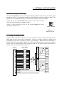
3.1 A/D Board Type Select Jumper
The CIO-EXP-BRIDGE16 may be used with either DAS08 or DAS16 family boards because the signal
assignments of the 37-pin connectors match those of the DAS08, and may be adapted to those of the
DAS16 with a C-EXP2DAS16-10 cable. Select the A/D board type via the JB10 jumper.
Jumper JB10 on the CIO-EXP-BRIDGE16, located near the 37-pin connector,
selects the A/D board family as DAS08 or DAS16.
Figure 3-1 shows the jumper set to use the CIO-EXP-BRIDGE16 with a
CIO-DAS08 family board.
'$6 '$6
Figure 3-1
DAS08/16 Select
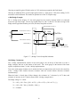
3.2 Setting The Output Channel
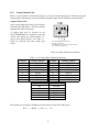
Jumpers labeled “CH SEL” located near the 37-pin connector select the A/D board channel that the
output from the active sensor will be connected to. There are 16 jumper positions for outputs, each
corresponding to one of the 16 output pins on the 37-pin connectors. When the board is connected to a
DAS08, only the first eight channels (labeled 0-7) can be used. When the board is connected to a DAS16,
any one of the 16 jumper positions can be selected. In each case, the jumper position corresponds to a
channel number on the A/D board. See Figure 3-2.
OUTPUT CHANNEL
SELECT JUMPER
37
0
36
1
35
2
34
3
33
4
32
5
31
6
7
18
8
17
9
16
10
15
11
14
12
13
13
12
14
11
15
10
9
8
7
INPUT 0
INPUT 1
INPUT 2
INPUT 3
INPUT 4
INPUT 5
INPUT 6
AMP
GAIN
1 OR 2.5
INPUT 7
8-CHANNEL MULTIPLEXER
30
8-CHANNEL MULTIPLEXER
37-Pin
CONNECTOR
INPUT 8
INPUT 9
INPUT 10
INPUT 11
INPUT 12
INPUT 13
MUX ADDR 4
MUX ADDR 3
INPUT 14
MUX ADDR 2
MUX ADDR 1
INPUT 15
2
Figure 3-2. Output Channel Jumper
JB6
CH SEL
JB16
Figure 3-3 is a diagram of the Channel Select jumper
blocks shown using channel 0 of the A/D board.
0 1 2 3 4 5 6 7
8 9 10 11 12 13 14 15
CHANNEL 0 SELECTED FOR SENSOR OUTPUT
Figure 3-3. Output Channel Select Jumpers
Place the jumper on the pin which corresponds to the A/D board's input channel.
A second set of jumpers is marked VEXC SEL (excitation voltage select). This jumper connects the
excitation voltage used for the bridge excitation to one of the A/D channels for monitoring. Installation
of this jumper is optional. If you decide to monitor excitation voltage, make sure you install this jumper
on a different channel number than that selected for the CH SEL jumper.
One individual channel must be selected for each bank of 16 EXP channels. For example, if you are
using several CIO-EXP-BRIDGE16 boards, the jumper setting for each board must be unique. If you
select channel 0 for the first board, do not use this channel for any of the other boards.
3.3 Configuring the A/D Board
3.3.1
DAS08 Family Setup
The input mode of the A/D board must be single-ended to be compatible with the CIO-EXP outputs.
Some of the boards in the DAS08 series have differential inputs that can be converted to single-ended
inputs. See the information shipped with your A/D board for conversion to single-ended inputs.
3.3.2
DAS16 Family Setup
The input mode of the A/D board must be single-ended to be compatible with the CIO-EXP outputs.
Most of the DAS16 series is switch selectable for either 8 differential or 16 single ended inputs. When
used with the CIO-EXP, set the switch to 16 channel, single-ended mode.
3.3.3
All A/D Boards
If you are using an A/D board with switch - selectable ranges, consider the application and determine the
best fit for range vs. expected voltage. For example, when measuring resistance such that the output of
the EXP board is expected to be in the range of 3 to 4.5 Volts, a unipolar 5V range would be the best
choice.
If the range on your A/D board is fully programmable, the software you use for measurement will
determine the range.
3
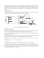
3.4 CONNECTING THE CIO-EXP-BRIDGE16 TO THE A/D BOARD
3.4.1
Connecting to a DAS08 Series A/D Board
A CIO-DAS08 series board may be connected directly through a C37FF series cable from the P1
connector on the CIO-EXP-BRIDGE16 to the A/D analog connector. The JB10 jumper should be left in
the DAS08 position as set at the factory.
3.4.2
Connecting to a DAS16 Series A/D Board
Connection to a DAS16 series board requires a special 37-conductor cable (C-EXP2DAS16-10) since pin
relationship of CIO-EXP and DAS16 signals is not 1:1.
Install the C-EXP2DAS16-10 cable connector labeled “MUX” into the P1 connector of the
CIO-EXP-BRIDGE16 board and the other end into the DAS16 series board’s analog connector.
3.4.3
Other A/D Boards
For other boards, use this connector diagram
(Figure 3-4) to construct a cable or call us and
discuss the possibility of a custom- manufactured
cable.
NC / LLGND
19
LLGND / OUTPUT 8
18
OUTPUT 9
The signals from the CIO-EXP-BRIDGE16 are
voltages from each channel and an analog ground.
There should be no voltage between analog
ground and power ground.
OUTPUT 10
15
OUTPUT 12
14
OUTPUT 14
OUTPUT 15
MUX ADDR 4
MUX ADDR 3
A jumper (CH SEL) selects which output channel
is read by the DAS08 or DAS16 board.
16
OUTPUT 11
OUTPUT 13
The MUX address lines control the setting of the
input channel multiplexer(s). When all are low,
the mux is set to Input 0. The lines are binary
coded where MUXADDR1 is the LSB and
MUXADDR4 is the MSB.
17
13
12
11
10
9
MUX ADDR 2
8
MUX ADDR 1
7
NC
NC
NC
NC
NC
NC
6
5
4
3
2
1
37
OUTPUT 0
36
OUTPUT 1
35
OUTPUT 2
34
OUTPUT 3
33
OUTPUT 4
32
OUTPUT 5
31
OUTPUT 6
30
OUTPUT 7
29
+5 VOLTS FROM PC
28
POWER GROUND
27
NC
26
NC
25
NC
24
NC
23
NC
22
NC
21
NC
20
NC
Figure 3-4. 37-Pin Output Connector Pinout
3.5 Powering The CIO-EXP-BRIDGE16
The CIO-EXP-BRIDGE16 can be powered through the 37-pin cable, the power screw terminal or the
Molex connector. The power that can be carried through the 37-pin connector is limited so we
recommend using this source only when a single CIO-EXP-BRIDGE16 is used.
4
The power required to run a CIO-EXP-BRIDGE16 is dependent on the board configuration. Remember
that additional power will be drawn when the CIO-EXP-BRIDGE16 is configured for resistance
measurement (bridge configuration) due to the current required for each bridge.
3.5.1
Power Source Switch
REM
X1
One of the switches on the eight-position DIP switch (S17)
near the output channel jumpers controls the source of the
+5V power to the CIO-EXP-BRIDGE16. Shown in Figure
3-5, it is the 3rd switch from the left.
When positioned down (ON, +5 COMP), +5V power is
drawn from the personal computer through the signal cable.
0.5V
1V
2V
4V
10V
X2.5
+5 COMP
GND
When positioned up (OFF, REM) , +5V power is taken from
the optional external 5V power connector (the Molex
connector labeled P19) or the +5V screw terminal
connection.
S17
Figure 3-5. Power Source Switch & Jumper
3.5.2
Powering with the 37-pin Connector
You can power the CIO-EXP-BRIDGE16 via the 37-pin cable. No more than one CIO-EXP-BRIDGE16
should be powered using the 37-pin cable.
This option is not available when using some A/D boards. If the A/D board you are using supplies +5V
at pin 29 (or at pin 1 when using the C-EXP2DAS16 signal cable), you can power the
CIO-EXP-BRIDGE16 through the 37 pin connector by setting the power select switch on S17 to “+5
COMP”.
3.5.3
Powering with the Molex Connector
The CIO-EXP-BRIDGE16 can be powered off the PC's power supply by connecting the optional external
5V power connector (the Molex connector labeled P19) to the PC’s power supply through a
C-MOLEX-10 cable. This cable has the same Molex connector that is used inside the PC and so can be
connected directly to the PC's power supply through one of the spare connectors. The cable is keyed, so
it should not be forced. When inserted properly it will slide easily and snap in place.
3.5.4
Powering Through the Power Screw Terminals
A set of screw terminals labeled +5V and GND are located next to the 37-pin connector, P2. You can
power the CIO-EXP-BRIDGE16 from a +5V ±5% power supply capable of at least 400 mA. For this
option, set the power select switch on S17 to “REM”.
CAUTION: The ground of the power supply and the ground of the personal computer should be tied
together through a heavy gauge wire. If you do not strap the two grounds together, a voltage difference
between theses grounds will affect measurements. If the potential exceeds the protection range of the
input circuits, the board may be damaged.
At this time, ignore the other screw terminals located next to the power and ground terminals. They are
needed only with certain sensors and will be explained in those sections.
5
3.6 Daisy-Chaining CIO-EXP-BRIDGE16 Boards
Connect one CIO-EXP-BRIDGE16 to another using a C37FF-# ribbon cable. Connect from P2 on the
‘upstream’ board to P1 on the ‘downstream’ board. Make sure each of the boards in the chain have a
unique channel selected (CH SEL jumper is set to a different number on each board).
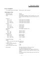
3.7 Connecting a Test Voltage
Make your initial test of the CIO-EXP-BRIDGE16 with a voltage signal of between -5 and 5V. If you
use an AC signal source, keep the frequency below 70Hz to avoid attenuation by the
CIO-EXP-BRIDGE16’s low pass filter. Each bridge input circuit has four screw terminals. These
terminals are shown in Figure 3-6 below.
To connect a voltage signal to the input circuit, connect the voltage to the
screw terminals as follows:
+SENSE
−P
Connect to + voltage.
Jumper this to −P.
Connect to ground.
No connection.
−SENSE
+P
+SENSE:
−SENSE :
−P:
+P:
CH0
Figure 3-6.
Input Screw Terminal Strip
The four screw terminals associated with each input circuit are labeled on the CIO-EXP-BRIDGE16 as
follows:
+SENSE
-P
-SENSE
+P
High side of input
Excitation voltage return
Low side of input
Excitation voltage
The use of the terminals is dependent on the type of sensor you have connected to the input circuit. The
nomenclature on the terminals has been chosen to be appropriate for bridge sensors.
3.8 Verifying The Installation
For verification of the installation, leave any switches or jumpers not mentioned above in their default
positions. Each of the gain switches (CH0 through CH15 and S17-7) should be off (toward the upper
edge of the board) for a gain of X1 (unity gain).
To verify the installation, use the InstaCal program installed on your computer. This software came with
your A/D board if you bought the board from the same manufacturer as the CIO-EXP-BRIDGE16. If
your A/D board is not from the same manufacturer but is compatible, please call technical support and
request a copy of InstaCal.
Use InstaCal's TEST option to verify that a signal present at one of the CIO-EXP-BRIDGE16 inputs can
be read. You will not need to set any jumpers other than those previously mentioned, and should not set
any switches or install any passive components until you have verified the installation.
6
4
CONFIGURATION FOR VOLTAGE MEASUREMENT
The CIO-EXP-BRIDGE16 is an amplification, signal conditioning and multiplexing front-end for DAS
boards. The inputs are suitable for connecting a voltage to the DAS board so it can be measured. The
CIO-EXP-BRIDGE16 is a one-of-sixteen multiplexer which means that for every channel in your DAS
board, you can multiplex sixteen different signals to it. You can expand the number of inputs of your
DAS board by sixteen for every CIO-EXP-BRIDGE16 board, up to the number of inputs on the DAS
board. For example, a DAS08 has eight inputs. Eight times sixteen is one hundred and twenty eight.
Thus, by using sixteen CIO-EXP-BRIDGE16 boards, you could bring 128 inputs into a PC with only one
DAS08 in one PC slot. Using a DAS16, up to 256 inputs could be accommodated.
It is unlikely that you purchased a CIO-EXP-BRIDGE16 to measure only voltages. The board was
designed for bridge sensors. For voltage only measurements, a CIO-EXP16 or CIO-EXP32 would be less
expensive and would do the same job.
However, if you have only one or two voltages to measure in addition to bridge sensors, you can use the
CIO-EXP-BRIDGE16.
4.1 Channel Selection
The General Configuration section describes the channel selection, setting the jumper and verifying the
installation and operation of the CIO-EXP-BRIDGE16 with your data acquisition board. Configure your
boards as described in that section before continuing with this section.
4.2 Powering the CIO-EXP-BRIDGE16
The General Configuration section describes the power selection options, setting the power select switch
and verifying the installation and operation of the CIO-EXP-BRIDGE16 with your data acquisition
board. Configure your boards as described in that section before continuing with this section.
4.3 Determining The Appropriate Gain
To accurately measure a voltage, the full scale of the signal should be matched to the full range of the
input circuit. (Most DAS boards have an input range of ±5V, which is the native range of the analog to
digital converter at the heart of the board. Some DAS boards include amplification on the input circuit to
allow the signal to be amplified to make better use of the resolution of the A/D.) For example, an input
signal which varies between 0 and 1 volt would only be using 1/10th of a ±5V A/D converter's
resolution. By switching the input signal of the DAS board to unipolar (no negative voltage) and
amplifying the input signal by 5, the entire range of the A/D converter is used and a higher resolution
measurement may be made. By adding this gain and selecting this range, the resolution on a 12-bit A/D
improves from 2.4 millivolts per bit to 0.24 millivolts per bit. If you needed to measure a change of 1
millivolt, you would need an amplification of 10.
In order to match your signals with the input range of the A/D board, you should do a similar calculation
and set switches on the CIO-EXP-BRIDGE16 for the required gain. Remember to make sure that the
settings in InstaCal match the switches on the DAS and CIO-EXP-BRIDGE16 boards.
If you are measuring signals greater than the maximum full scale range of the A/D, see the section on
attenuation.
7
To choose a switch-selectable amplification, here are the calculations you need to perform:
Divide the full range selected for the A/D board by the full range of the signal to be measured to
determine the maximum gain of the CIO-EXP board. For best resolution, use the highest gain possible
up to the calculated maximum gain.
For example, if the A/D board is to be used at a range of ±5V, the full range of the board is 10. If your
signal ranges between -0.5 volts and 0.5 volts, the full range of the signal is 1 volt. Divide 10 by 1 for a
result of 10. That is the maximum gain you can use.
If your signal is unipolar and ranges less than 0 to 5V, you would likely choose the 5V unipolar range for
the A/D board (if available). Given an input signal ranging from 0 to 0.5 volts, the full range of the
signal is 1/2 volt. Divide 5 (the full range of the A/D) by 0.5 (the full range of the signal for a result of
10. That is the maximum gain you can use.
4.4 Setting the Gain
Gain (amplification) allows you to boost your signal to take full advantage of the resolution of the A/D
converter. However, when amplifying a signal, any noise is amplified as well.
Amplification for ALL channels (board output gain) is switch selectable (S17) for X1 or X2.5.
Input amplification for EACH CHANNEL is switch selectable (CH0 through CH15) for X1, X10, X100
or X1000. A user-specified gain may be set by supplying a precision resistor at position RX### and
setting the “U” option on switch CH ## to ON.
4.4.1
Setting Board Gain
REM
X1
There is a switch on DIP switch block S17
labeled X1 and X2.5. Sliding this switch down
amplifies the output of the multiplexers by 2.5.
The factory default position (up) has a gain of 1
(unity). Refer to Figure 4-1.
S17
0.5V
1V
2V
10V
4V
X2.5
+5 COMP
GND
The X2.5 gain switch is useful in some voltage
and bridge measurements. If you desire a
voltage gain of 2.5, 25, 250 or 2500, set this
switch down.
Figure 4-1. Board Output Gain Switch Location
For voltage measurements, a gain of 2500 is very high and will reduce your signal to noise ratio.
The effect of this switch is multiplicative with respect to the individual channel gains. For example, if
you have set an input channel gain to X100 and the board output gain to X2.5, the signal is amplified by
250 before it reaches the A/D board.
8
4.4.2
Setting Channel Gain
Select a gain (higher than unity) by moving the switch
for that gain down. All other switches should be left in
the UP position.
N
O
X100
X1000
X10
U
A custom gain may be selected on the
CIO-EXP-BRIDGE16 by installing a precision resistor
and setting the switch marked “U” (User) in the down
position. See Table 4-1 following for board positions
and some sample gain values.
CH0
GAIN SWITCHES FOR CHANNEL 0
SET FOR A GAIN OF 10.
PUSH SLIDER TO 'ON' (DOWN) TO SELECT GAIN
ALL OTHERS TO BE OFF (UP)
Figure 4-2. Input Channel Gain Select Switch- Typ.
Channel
0
1
2
3
4
5
6
7
Table 4-1. Resistor Positions for User-Selected Gains
Resistor Position
Channel
Resistor Position
RX100
8
RX108
RX101
9
RX109
RX102
10
RX110
RX103
11
RX111
RX104
12
RX112
RX105
13
RX113
RX106
14
RX114
RX107
15
RX115
Gain
100
200
500
700
800
Resistor Value
364 Ohms
161 Ohms
40 Ohms
17 Ohms
10 Ohms
The equation for selecting the USER gain resistor is:
RUSER = [40000 / (Gain−1)] −40
Amplifying a signal on one channel will not affect readings on another channel.
9
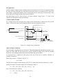
4.5 Attenuation
If your signal is in a range greater than the full scale range of the A/D, you must either set the A/D for a
higher full scale range (if available) or divide (attenuate) the signal until the result is less than or equal to
the A/D’s full scale range. This section describes signal attenuation.
INPUT
A voltage divider is constructed from a pair of
precision resistors selected according to the
equation:
Ra
OUT
Volts In
Attenuation (A) = (Ra + Rb) / Rb
See Figure 4-3 at right for the schematic of a
voltage divider.
Volts Divided
Rb
PC GROUND
PC GROUND
Figure 4-3. Voltage Divider
For example, if your signal is 0 to 10V, it must be attenuated to 5V max. for an attenuation of 2:1 or
simply 2.
Using 10k resistors: 2 = (10K + 10K) /10K.
For any attenuation, pick a suitable resistor for Rb. Then use this formula to calculate Ra:
Ra = (A−1) x Rb
You will need to construct the voltage divider remote from the CIO-EXP-BRIDGE16 board.
4.6 Connecting Voltage Signals
Voltage input signals can be single-ended or differential. In addition, the full scale may have to be
matched to the range of the CIO-EXP-BRIDGE16 and DAS board combination using amplification or
attenuation. To connect a voltage and make an accurate measurement, both of these factors must be
considered (see section 4.3).
After the range has been matched and the signal connected, the measurement is made using the DAS
board and software. You can use InstaCal to display the value read on any channel of the
CIO-EXP-BRIDGE16.
Each input circuit has four screw terminals associated with it. These
terminals are shown in Figure 4-4. To connect a voltage signal to the input
circuit you need only use three screw terminals. These are:
+SENSE
−P
−SENSE
+P
+SENSE: High side of a differential or single-ended voltage signal.
−SENSE: Signal low, or CH LO on a DAS board. Must be jumpered to −P
for single-ended.
−P:
Ground of a differential voltage signal or Low side of a single ended signal.
CH0
Figure 4-4.
Input Screw Terminal Strip
10
4.6.1
Single Ended
A single-ended input has two wires connected to the CIO-EXP-BRIDGE16; a signal high and a Low
Level Ground (LLGND). The LLGND signal must be the same ground the PC is on. Single-ended mode
is selected by installing a jumper between the signal input low (−SENSE) and ground (−P). The -SENSE
terminal is then connected to the signal ground and the +SENSE terminal is connected to the signal.
4.6.2
Floating Differential
A floating differential input has two wires from the signal source and a 10K ground reference resistor
installed at the CIO-EXP-BRIDGE16 input. The two signals from the signal source are Signal High and
Signal Low. The reference resistor is connected between the CIO-EXP-BRIDGE16 (−SENSE) and (−P)
pins and the Signal Low is connected to the -SENSE terminal. The +SENSE terminal is connected to the
Signal High.
A floating differential hookup is handy when the signal source is floating with respect to ground, such as
a battery. The floating differential input will reject up to 10V of EMI energy on the signal wires.
CAUTION! Determine that the signal source is actually floating. Check it with a voltmeter before
risking the CIO-EXP-BRIDGE16 and PC!
4.6.3
Fully Differential
A differential signal uses three wires from the signal source. The signals are Signal High, Signal Low
and Signal Ground (LLGND). Signal High is connected to the +SENSE terminal and Signal Low is
connected to the -SENSE terminal. The ground reference must be connected to the -P terminal.
A differential connection allows you to connect to a signal source with a ground that is different than the
PC ground, but less than 10V difference, and still measure the signal.
EXAMPLE: A laboratory instrument with its own wall plug. Sometimes there is a voltage between wall
outlet grounds.
4.7 Verifying the Installation
To verify the installation, use the InstaCal program installed on your computer. This software came with
your A/D board if you bought the board from the same manufacturer as the CIO-EXP-BRIDGE16. If
your A/D board is not from the same manufacturer but is compatible, please call technical support and
request a copy of InstaCal.
Use InstaCal's TEST option to verify that a signal present at one of the CIO-EXP-BRIDGE16 inputs can
be read. When using an AC signal source, keep the frequency below 70Hz to avoid attenuation by the
low pass filter.
11
5
CONFIGURATION FOR RESISTANCE MEASUREMENT
Resistance measurements are made using the CIO-EXP-BRIDGE16 by constructing a resistor “bridge”
containing known resistor values that are to be compared to the resistor value to be measured. This is
known as a Wheatstone Bridge. The typical application is a strain gauge.
Strain gauge sensors are variable-resistance devices. When installed in one leg of the resistor bridge (as
the “unknown” resistor, their value can be measured. The Wheatstone Bridge circuit is extremely
sensitive to changes in resistance in one leg relative to the others. There are various types of bridge
sensors, but the descriptions and examples here are for strain gauges.
5.1 Channel Select
The General Configuration section describes the channel selection, setting the jumper and verifying the
installation and operation of the CIO-EXP-BRIDGE16 with your data acquisition board. Configure your
boards as described in that section before continuing with this section.
5.2 VEXC Jumper Select
There is a set of jumpers near the 37 pin connector labeled “VEXC SEL”, which stands for channel
excitation voltage select. This jumper will connect the on-board excitation voltage to one of the A/D
board channels so that it may be measured. OMEGA Engineeering does not use a measurement
of the excitation voltage in any of its software. You do not need to set this jumper if you are using the
CIO-EXP-BRIDGE16 with OMEGA Engineeering software, or with packages such as Labtech
Notebook which use the Universal Library. Use this jumper only with software from other
manufacturers that specifically require it.
5.3 Powering The CIO-EXP-BRIDGE16
There are two power issues to address. The first is the source of the 5 volt power to the board. The
second is the source of the bridge excitation voltage power.
5.3.1
Selecting the Power Source for the Board
The General Configuration section describes the power selection options for powering the
CIO-EXP-BRIDGE16 itself. Configure your boards as described in Powering the CIO-EXP-BRIDGE16
in the General Configuration section before continuing with this section.
5.3.2
Selecting the Power Source for the Excitation Voltage
Bridge sensors consume a lot of power. In some cases the bridge sensors consume so much power that if
fully populated with 16 sensors, the on-board excitation circuit would not have adequate power to supply
all 16 sensors. This is an extreme case but is indicative of the attention you must pay to power
requirements when using bridge sensors.
Also, when selecting the power source for the excitation voltage, consider the voltage you will use for
excitation. The options available are 0.5, 1, 2, 4 and 10V. In general, higher excitation voltages are
better because a higher voltage increases the difference between the balance points of the bridge circuit,
which increases the accuracy of your measurement. The excitation voltage must be less than the source.
12
Jumper JB11 (Figure 5-1), located near the bottom edge of the board,
selects the source of the bridge excitation voltage. The three choices
are +5V (the same 5V source chosen for board power above), +12V
(from the PC through the 37 pin connector) or +PEXT (an external
power supply connected at the ±P EXT screw terminal).
JB11
+P EXT
+12V
+5V
Figure 5-1.
Output Gain & Power Select
If you choose a separate power supply, it must be a floating, isolated supply (one with three terminals).
Do not tie the GND and −V terminal together. It must not exceed +15V.
The +5V and +12V jumpers are only valid with CIO-DAS08 family boards. The +12V jumper is not
valid with the CIO-DAS08-AO and -PGx. For more information on excitation voltages, refer to the
section on bridge sensors.
+5V Excitation Voltage Source
If your choice for the excitation voltage source is +5V, you may choose a 0.5V, 1V, 2V or 4V excitation
voltage for your bridge sensors. The +5V option is always available, since +5V is required to power the
CIO-EXP-BRIDGE16.
+12V Excitation Voltage Source
If your choice for the excitation voltage source is +12V PC power, you have the choice of 0.5, 1, 2, 4, or
10 volt excitation for your bridge sensors. The option to power from the PC 12 volt supply exists only
with DAS08 family boards, except that +12V is not valid with the CIO-DAS08-AO or PGA.
+PEXT Excitation Voltage Source
An external power supply can be used. If you choose a separate power supply, it must be a floating, or
isolated supply (one with three terminals). Do not tie the GND and -V terminal together). Output voltage
must not exceed +15V. If your power supply is not floating, it is likely that you will create a ground loop
(current flow in the ground lines). A ground loop will induce an error in your reading. Connect the
power supply to the CIO-EXP-BRIDGE16 at the terminals labeled −PEXT and +PEXT on the screw
terminal block located adjacent to the 37-pin connector, P2.
5.3.3
Selecting the Excitation Voltage
REM
X1
DIP switch S17 has five switches to select bridge
excitation voltage. Only set one ON. All others
must be OFF.
Figure 5-2 shows the switch and the excitation
power source jumper set for the factory defaults.
Excitation is set for 10V ON. Power source must
be set to +12V (as shown in Figure 5-1) or +PEXT.
0.5V
1V
2V
4V
10V
+5 COMP
X2.5
GND
Do not select an excitation voltage at the switch
that exceeds the excitation power supply voltage.
S17
Figure 5-2. Excitation Voltage Select Switches
13
5.4 Determining the Appropriate Gain
To accurately measure a voltage, the full scale of the signal should be matched to the full range of the
input circuit. (Most DAS boards have an input range of ±5V, which is the native range of the analog to
digital converter at the heart of the board. Some DAS boards include amplification on the input circuit to
allow the signal to be amplified to make better use of the resolution of the A/D.) For example, an input
signal which varies between 0 and 1 volt would only be using 1/10th of a ±5V A/D converter's
resolution. By switching the input signal of the DAS board to unipolar (no negative voltage) and
amplifying the sign wave signal by 5, the entire range of the A/D converter is used and a higher
resolution measurement may be made. By adding this gain and selecting this range, the resolution on a
12-bit A/D improves from 2.4 millivolts per bit to 0.24 millivolts per bit. If you needed to measure a
change of 1 millivolt, you would need an amplification of 10.
In order to match your signals with the input range of the A/D board, you should do a similar calculation
and set switches on the CIO-EXP-BRIDGE16 for the required gain. Remember to make sure that the
settings in InstaCal match the switches on the DAS and CIO-EXP-BRIDGE16 boards.
When using strain gauges, the expected output from the sensor should be calculated and the gain of the
CIO-EXP-BRIDGE16 set accordingly. There are some examples at the end of this chapter detailing
these calculations. You may also find it helpful to refer to the Appendix for additional strain gauge
information.
5.5 Setting the Gain
Once you have determined the gain required for your application, set the gain of the
CIO-EXP-BRIDGE16 using the following guide.
Amplification for ALL channels (board output gain) is switch selectable (S17) for X1 or X2.5.
Input amplification for EACH CHANNEL is switch selectable (CH0 through CH15) for X1, X10, X100
or X1000. A user-specified gain may be set by supplying a precision resistor at position RX### and
setting the “U” option on switch CH ## to ON.
5.5.1
Setting Board Gain
REM
X1
There is a switch on DIP switch block S17
(Figure 5-3) labeled X1 and X2.5. Sliding this
switch down amplifies the output of the
multiplexers by 2.5. The factory default
position (up) has a gain of 1 (unity).
S17
0.5V
1V
2V
10V
4V
X2.5
+5 COMP
GND
The X2.5 gain switch is useful in some voltage
and bridge measurements. If you desire a
voltage gain of 2.5, 25, 250 or 2500, set this
switch down.
Figure 5-3. Board Gain
The effect of this switch is multiplicative with respect to the individual channel gains. For example, if
you have set an input channel gain to X100 and the board output gain to X2.5, the signal is amplified by
250 before it reaches the A/D board.
14
5.5.2
Setting Channel Gain
There is a gain switch for each channel (Figure 5-4). Set the input channel gain to match the expected
voltage output of the bridge you are measuring to the input range of the A/D board as described above.
Channel Gain Switch
CH0
Select a gain (higher than unity) by moving the
switch for that gain down. All other switches
should be left in the UP position.
N
O
X100
X1000
X10
U
A custom gain may be selected on the
CIO-EXP-BRIDGE16 by installing a precision
resistor and setting the switch marked “U”
(User) in the down position. See Table 5-1
below for positions and some sample gain
values.
GAIN SWITCHES FOR CHANNEL 0
SET FOR A GAIN OF 10.
PUSH SLIDER TO 'ON' (DOWN) TO SELECT GAIN
ALL OTHERS TO BE OFF (UP)
Figure 5-4. Input Channel Gain Switches
Channel
0
1
2
3
4
5
6
7
Table 5-1. User-Specified Gain Resistor Positions
Resistor Position
Channel
Resistor Position
RX100
8
RX108
RX101
9
RX109
RX102
10
RX110
RX103
11
RX111
RX104
12
RX112
RX105
13
RX113
RX106
14
RX114
RX107
15
RX115
Gain
100
200
300
500
700
800
Resistor Value
364 Ohms
161 Ohms
130 Ohms
40 Ohms
17 Ohms
10 Ohms
The equation for selecting the USER gain resistor between X100 and X1000 gain is:
RUSER =
(40000 / ( Gain − 1) ) − 40
15
5.6 Configuring the Bridge
As mentioned earlier in this chapter, resistance measurements are made by constructing a bridge
containing precision resistors with known values against which the unknown resistor is to be compared.
In strain gauge applications, the strain gauge sensor itself may make up a quarter of this bridge, half of
this bridge or the entire bridge. Examples of each of these configurations follow.
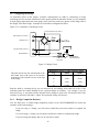
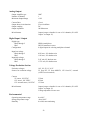
Figure 5-5 is a schematic of the bridge circuit.
EXCITATION VOLAGE (+)
EXCITATION. VOLTS (+)
A
B Arm
Null Pot
SENSE LOW (-)
C
D
GAIN SW
EXCITATION VOLTS (-)
SENSE HIGH (+)
AMP
TO CHANNEL
MULTIPLEXOR
80Hz Low
Pass Filter
Figure 5-5. Bridge Circuit
Resistance Change vs. Sense Voltage Change
Leg
+ Ohms
- Ohms
- Volts
+ Volts
A
This table shows how the measurement at the
A/D board varies with respect to an increase
or decrease of the resistance in one of the legs
of the bridge.
B
- Volts
+ Volts
C
- Volts
+ Volts
D
+ Volts
- Volts
Read the table by selecting the leg you are interested in and looking across that row to the ±Volts
indication under the column heading for the expected change in resistance. For example, if you are
interested in leg ‘A’ and want to know what the relative change in volts at the A/D board will be if the
resistance is increased, look under + Ohms. The measured voltage will increase.
5.6.1
Bridge Completion Resistors
You will likely have to install bridge-completion resistors in the CIO-EXP-BRIDGE16 to match the
resistance of the external gauge:
If you are using a ¼ bridge, you will need to install three precision resistors to complete the
bridge.
If you are using a ½ bridge, you will need to install two resistors to complete the bridge.
If you are using a full bridge, there are no resistors to install.
16
Referring back to Figure 5-5, the legs of the bridge are labeled A, B, C and D. Table 5-3 below matches
the legs of the bridge to the resistor number nomenclature that appears on the CIO-EXP-BRIDGE16.
Channel
0
1
2
3
4
5
6
7
8
9
10
11
12
13
14
15
Bridge A
RX1
RX7
RX13
RX19
RX25
RX31
RX37
RX43
RX49
RX55
RX61
RX67
RX73
RX79
RX85
RX91
Table 5-3. Bridge Resistor Identities
Bridge B
Bridge C
Bridge D
RX2
RX3
RX4
RX8
RX9
RX10
RX14
RX15
RX16
RX20
RX21
RX22
RX26
RX27
RX28
RX32
RX33
RX34
RX38
RX39
RX40
RX44
RX45
RX46
RX50
RX51
RX52
RX56
RX57
RX58
RX62
RX63
RX64
RX68
RX69
RX70
RX74
RX75
RX76
RX80
RX81
RX82
RX86
RX87
RX88
RX92
RX93
RX94
Arm
RX5
RX11
RX17
RX23
RX29
RX35
RX41
RX47
RX53
RX59
RX65
RX71
RX77
RX83
RX89
RX95
Null Pot
R6
R12
R18
R24
R30
R36
R42
R48
R54
R60
R66
R72
R78
R84
R90
R96
Some values of precision resistors are available from OMEGA Engineeering.
Note: Positions marked D1 through D64 are empty and are not used.
5.6.2
Nulling Potentiometers & Arm Resistor
Each circuit has a position for a nulling potentiometer and associated Arm resistor. The purpose of the
nulling arm is to allow you to zero the reading of strain at a given strain position. There is no formula to
use to select the nulling potentiometer and arm resistor. Bridge resistor values and total gain selected for
the CIO-EXP-BRIDGE16 will affect adjustability for a given nulling circuit. An average value for the
arm resistor is 10k ohms. Start with that and adjust as required.
5.6.3
Strain Gauge Bridge Configuration Examples
Following are three typical strain gauge bridge configurations. They are by no means the only way to
connect a strain gauge. For example, there is no rule that says the ‘A’ leg must be the strain gauge on a
¼ bridge implementation.
The examples below show how to translate strain to input voltage for the strain gauge
configuration used to measure simple bending strain. Other types of stress and strain: axial,
torsion, shearing, etc. are beyond the scope of this description. These examples can be used to as a
guide for calculating the bridge voltage in your own application, and thus help you select the proper
amplifier gain and excitation voltage.
The use of quarter bridge, half bridge and full bridge strain gauges are described.
17
The Application:
In these examples, imagine a beam extending out from a fixed point on a wall. Force is applied to deflect
the end of the beam downward. We know that the maximum strain to be measured will be 250µε (250
micro strain). Knowing the amount of force required and the size of the beam is not necessary, since
strain relates to the change in length of the surface of interest.
The Strain Gauge will be a metal foil type, 350 ohms resistance, Gauge Factor = 2. Refer to the
Appendix for information on these specifications.
A Quarter Bridge Example
For ¼ bridge circuits, the strain gauge has a single resistive element that is connected as one leg of the
bridge. The other three legs must be populated with the precision completion resistors.
EXCITATION VOLAGE (+)
EXCITATION. VOLTS (+)
A
B Arm
Null Pot
SENSE LOW (-)
C
D
GAIN SW
EXCITATION VOLTS (-)
SENSE HIGH (+)
AMP
80Hz Low
Pass Filter
TO CHANNEL
MULTIPLEXOR
Figure 5-6. ¼ Bridge Circuit - Simplified
Quarter-Bridge Calculations
The strain gauge is applied to the top of the beam. This strain gauge takes the place of resistor A (see
Figure 5-6). Three other 350 ohm resistors (B, C and D) complete the bridge circuit. These are installed
by the user in locations provided on the board or attached to the screw terminals.
As downward force is applied, the strain gauge on the top of the beam is stretched. Therefore, its
resistance increases by:
Strain Gauge increase = 350 ohm x 250 x 10-6 x 2
= +0.175 ohm
Thus the value of gauge A (under tension) will be 350.175 ohms when the strain on the beam is +250µε.
Initially, choosing an excitation voltage of 10V, the bridge voltage is:
Vbr = 10V { (350 / 700) - [350 / (350 + 350 )) ] } = 0V
After a downward force is applied:
Vbr = 10V { (350 / 700) - [350 / (350 + 350.175)] }
Vbr =
1.25mV
18
Choosing an amplifier gain of X1000 results in 1.25V maximum presented to the DAS board.
Choosing an additional X2.5 (overall output gain) results in a total gain of 2500, thus sending 3.125V
maximum to the DAS board. This makes an optimum use of the 5V unipolar range.
A Half Bridge Example
For a ½ bridge circuit (Figure 5-7), the strain gauge has two resistive elements which are connected
across two legs of the bridge. The two legs would always be A & C or B & D. The other two legs of the
bridge must be populated with the precision (350 ohm) completion resistors.
EXCITATION VOLAGE (+)
EXCITATION. VOLTS (+)
A
B Arm
Null Pot
SENSE LOW (-)
C
D
GAIN SW
EXCITATION VOLTS (-)
SENSE HIGH (+)
AMP
80 Hz Low
Pass Filter
TO CHANNEL
MULTIPLEXOR
Figure 5-7. ½ Bridge Circuit- Simplified Schematic
Half Bridge Calculations
The ½ bridge implementation consists of two strain gauges; one on the top of the beam (as in the ¼
bridge example) and one on the bottom of the beam. The strain gauge on the bottom of the beam
replaces completion resistor C in the ¼ bridge implementation.
Two active strain gauge elements (one in tension and one in compression) result in twice the sensitivity
of the ¼ bridge. (One element increases resistance while the second element decreases resistance
simultaneously.)
When the beam is forced down (250µε change), the resistance in C decreases by 0.175 ohm, and
resistance A increases by 0.175 ohm as shown in the ¼ bridge example above.
The bridge voltage Vbr is then:
Vbr = 10V { (350 / 700) - [(350 - 0.175) / ( (350 - 0.175) + (350 + 0.175) ) ] }
Vbr = 10V {(350 / 700) - [(349.825) / (700) ] }
Vbr = 2.500mV
19
Choosing Gain = X1000 would result in 2.5V being applied to the DAS board. Choosing Gain = X2500
(X1000 on the input channel and X2.5 on the output) could result in an amplified voltage that’s out of the
DAS board’s range. In this case, the excitation voltage could be reduced to 4V, reducing the bridge
voltage to 1.00mV. A gain selection of 2500 would then present a maximum voltage of 2.5V to the DAS
board.
Full Bridge Example
Full bridge strain gauges consist of all four bridge resistors (Figure 5-8). Obviously, no bridge
completion resistors are installed on the board when using this configuration.
EXCITATION VOLAGE (+)
EXCITATION. VOLTS (+)
Arm
A
B
Null Pot
SENSE LOW (-)
C
GAIN SW
EXCITATION VOLTS (-)
D
SENSE HIGH (+)
AMP
80Hz Low
Pass Filter
TO CHANNEL
MULTIPLEXOR
Figure 5-8. Full Bridge - Simplified Schematic
Full bridge calculations
With four active strain gauge elements, these are four times more sensitive than a 1/4 bridge. All four
resistors are strain gauges and are attached to the beam in the following configuration:
Gauge resistors C and B are on the bottom. Their resistance decreases under the resultant compression
(but bridge voltage increases).
Gauge resistors D and A are on the top of the beam. Their resistance increases under the resultant tension
(and bridge voltage likewise increases), equal in magnitude to the changes in D and A.
Vbr = 10V {[(350 + 0.175) / ((350 + 0.175) + (350 - 0.175))] - [(350 - 0.175) / ((350 - 0.175) + (350 +
0.175) ) ] }
Vbr = 10V { [ (350 + 0.175) / 700] - [ (349.825) / 700] }
Vbr = 5.00mV
Choosing a gain of X1000 presents 5V to the DAS board covering its entire 5V unipolar range.
An excitation voltage of 4V could be been used in combination with a gain of 2500 (X1000 on the input
channel and X2.5 on the output). This would also result in 5V to the DAS board. The advantage to using
a lower excitation voltage is that it causes less power dissipation on the strain gauge element itself,
reducing thermal expansion from self-heating.
20
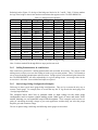
6
SPECIFICATIONS
Power consumption
+5V (excludes any power to bridges)
250mA typical, 350mA maximum
Analog input section
Input amplifier type
Number of channels
Gains
Gain Error
Gain = 1, 2.5
Gain = 10, 25
Gain = 100, 250
Gain = 1000, 2500
Linearity
Gain = 1, 2.5
Gain = 10, 25
Gain = 100, 250
Gain = 1000, 2500
Input Offset
Gain TC
Gain = 1
Gain = 100
Gain = 1000
Input Offset TC
Gain = 1, 2.5
Gain = 10, 25
Gain = 100, 250
Gain = 1000, 2500
INA102
16 differential
Each channel individually switch selectable for X1, X10,
X100 or custom and board gain switch selectable for X1 or
X2.5
0.01% typical, 0.15% maximum
0.02% typical, 0.35% maximum
0.05% typical, 0.40% maximum
0.20% typical, 0.90% maximum
0.045% typical
0.045% typical
0.075% typical
0.15% typical
Each channel adjustable to zero
10ppm/°C typical
15ppm/°C typical
20ppm/°C typical
20µV/°Ctypical
6µV/°C typical
5.1µV/°C typical
5.1µV/°C typical
Common Mode Range
±10V
CMRR
Gain = 10, 25, 100, 250, 1000, 2500 100dB typical
Gain = 1, 2.5
94dB typical
Channel to channel settling time
5V step to .01%
250µs
Absolute maximum input voltage
±15V
Miscellaneous
Each input channel has a 79Hz low pass filter
X2.5 gain is adjustable for zero error
Jumper selects compatibility with DAS08 or DAS16 series
Locations provided for bridge completion resistors for each
channel.
Locations provided for bridge nulling pots and resistors for
each channel
21
Analog Output
Output Amplifier type
Number of channels
Maximum Output Range
OP07
1
±10V
Current Drive
Output short-circuit duration
Output coupling
Output impedance
±5 mA
25 mA indefinite
DC
100 Ohms max
Miscellaneous
Output jumper selectable for one of 16 channels (P1 & P2
Output - to Output 15)
Digital Input / Output
Digital type
DIn 0 through 2
DIn 3
Configuration
Input low voltage
DIn 0 through 2
DIn 3
Input high voltage
DIn 0 through 2
DIn 3
HI508A multiplexer
2N2222 transistor inverter
4 digital inputs for selecting multiplexer channel
0.8V max, -4V absolute min
1.0V max, -4V absolute min
2.4V min, 9V absolute max
1.27V min, 9V absolute max
Voltage Excitation Section
Excitation voltages
Sources for excitation voltage
Current
5V source, 4V VEXC
12V source, 10V VEXC
15V external source, 10 VEXC
Miscellaneous
10V, 4V, 2V, 1V, 0.5V
5V from PC, 5V from MOLEX, 12V from PC, external
(±PEXT screw terminal)
333mA
833mA
1333mA
Output jumper selectable for one of 16 channels (P1 & P2
Output - to Output 15)
Voltage adjustable for zero error
Environmental
Operating temperature range
Storage temperature range
Humidity
0 to 60°C
-40 to 100°C
0 to 90% non-condensing
22
7
APPENDIX
7.1 About Strain Gauges
7.1.1
What Are Strain Gauges?
A Strain Gauge is a variable resistance device whose resistance changes in proportion to the
amount it is stretched or compressed. Physically it is an etched metal-foil in a grid pattern that is
glued to any surface which undergoes strain. The output is a dimensionless quantity defined as
change in length and whose symbol is ε. A micro-strain of “1” means that length of the surface
of interest has changed by 1 ppm. The ratio of resistance change to strain change is known as the
Gauge Factor (GF). Typical metal foil strain gauges have Gauge Factors of 2 to 2.1. This means
that the resistance will change twice as much as the strain does. A change of 1 micro-strain
means that the resistance of the strain gauge has changed by 2 ppm or .0002% (.0001% x 2). For
a 350 ohm strain gauge with GF = 2, a 1µε change results in a resistance change of:
ε
ε
ε
Resistance change =
=
=
7.1.2
[SG Resistance]
[ 350 ohm ]
0.0007 ohm
x [change in length]
x [ .000001]
x [Gauge Factor]
x [2]
Specification of Strain Gauges
Metal Foil gauges are available in 120, 350 and 1000 ohms. Semiconductor strain gauges exist
and have resistance of up to 10000 ohms. They can readily be used with the
CIO-EXP-BRIDGE16, but may not be as linear as metal foil gauges.
Maximum strain allowed is 3% to 5% depending on type and thickness of strain gauge material.
ε
This means a limit of 30,000 to 50,000µε or a maximum resistance change of 6% to 10%.
Strain Gauges are typically used to calculate a change in strain; that is, the difference between the
unstrained and the strained state.
7.2 Reference Material for Application of Strain Gauges
The Bonded Electrical Resistance Strain Gage, First Edition
by William M. Murray and William R. Miller.
1992, 424 pages ISBN: 0-19-507209-X
Available from Society for Experimental Mechanics, order # OX-2.
Strain Gage Users’ Handbook , First Edition.
1992, 424 pages. ISBN: 0-912053-36-4
Published by Society for Experimental Mechanics, order #ELS-017
23
The Art of Practical and Precise Stain Based Measurement
by James Pierson.
1992, 400 pages in 3-ring binder . ISBN: 1-895976-00-6
Available from Society for Experimental Mechanics, order # JP-001
Strain Gage and Transducer Techniques
1984, 72 pages.
Published by Published by Society for Experimental Mechanics, order # S-023
Society for Experimental Mechanics
7 School St.
Bethel CT 06801
(203) 790-6373
24
EC Declaration of Conformity
CIO-EXP-BRIDGE16
Part Number
Bridge inputs for ISA bus
Description
to which this declaration relates, meets the essential requirements, is in conformity with, and CE marking has been
applied according to the relevant EC Directives listed below using the relevant section of the following EC standards
and other normative documents:
EU EMC Directive 89/336/EEC: Essential requirements relating to electromagnetic compatibility.
EU 55022 Class B: Limits and methods of measurements of radio interference characteristics of information
technology equipment.
EN 50082-1: EC generic immunity requirements.
IEC 801-2: Electrostatic discharge requirements for industrial process measurement and control equipment.
IEC 801-3:
equipment.
Radiated electromagnetic field requirements for industrial process measurements and control
IEC 801-4: Electrically fast transients for industrial process measurement and control equipment.
Carl Haapaoja, Director of Quality Assurance
OMEGA Engineering Inc.
One OMEGA Drive,
Stamford,Connecticut 06801
(800) 872-9436
Fax: (203) 359-1660
E-mail: [email protected]
www.omega.com