1
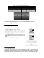
CyDAS Series
CYEXP GP
8-Channel
General Purpose
Multiplexing Panel
USER’S MANUAL
VER. 2
• JAN 2001
&
No part of this manual may be reproduced without permission.
CyberResearch®, Inc.
www.cyberresearch.com
25 Business Park Dr., Branford, CT 06405 USA
203-483-8815 (9am to 5pm EST) FAX: 203-483-9024
©Copyright 2001
All Rights Reserved.
January 2001
The information in this document is subject to change without prior notice in order
to improve reliability, design, and function and does not represent a commitment
on the part of CyberResearch, Inc.
In no event will CyberResearch, Inc. be liable for direct, indirect, special,
incidental, or consequential damages arising out of the use of or inability to use
the product or documentation, even if advised of the possibility of such damages.
This document contains proprietary information protected by copyright. All rights
are reserved. No part of this manual may be reproduced by any mechanical,
electronic, or other means in any form without prior written permission of
CyberResearch, Inc.
TRADEMARKS
“CyberResearch” and “CYEXP GP” are trademarks of CyberResearch, Inc. Other
product names mentioned herein are used for identification purposes only and
may be trademarks and/or registered trademarks of their respective companies.
• NOTICE •
CyberResearch, Inc. does not authorize any CyberResearch product for use in life
support systems, medical equipment, and/or medical devices without the written
approval of the President of CyberResearch, Inc. Life support devices and
systems are devices or systems which are intended for surgical implantation into
the body, or to support or sustain life and whose failure to perform can be
reasonably expected to result in injury. Other medical equipment includes devices
used for monitoring, data acquisition, modification, or notification purposes in
relation to life support, life sustaining, or vital statistic recording. CyberResearch
products are not designed with the components required, are not subject to
the testing required, and are not submitted to the certification required to ensure
a level of reliability appropriate for the treatment and diagnosis of humans.
i
ii
Table of Contents
1 INTRODUCTION . . . . . . . . . . . . . . . . . . . . . . . . . . . . . . . . . . . . . . . . . . . . . . . . . . . . . . . . . . . . . . 1
2 SOFTWARE INSTALLATION . . . . . . . . . . . . . . . . . . . . . . . . . . . . . . . . . . . . . . . . . . . . . . . . . . 3
3 GENERAL CONFIGURATION . . . . . . . . . . . . . . . . . . . . . . . . . . . . . . . . . . . . . . . . . . . . . . . . . . 5
3.1 A/D Board Type Select Jumper . . . . . . . . . . . . . . . . . . . . . . . . . . . . . . . . . . . . . . . . . . . . . . 5
3.2 Setting The Output Channel . . . . . . . . . . . . . . . . . . . . . . . . . . . . . . . . . . . . . . . . . . . . . . . . . 5
3.3 Configuring the A/D Board . . . . . . . . . . . . . . . . . . . . . . . . . . . . . . . . . . . . . . . . . . . . . . . . . . 6
3.3.1 DAS08 Family Setup . . . . . . . . . . . . . . . . . . . . . . . . . . . . . . . . . . . . . . . . . . . . . . . . . . . 6
3.3.2 DAS16 Family Setup . . . . . . . . . . . . . . . . . . . . . . . . . . . . . . . . . . . . . . . . . . . . . . . . . . . 6
3.3.3 All A/D Boards . . . . . . . . . . . . . . . . . . . . . . . . . . . . . . . . . . . . . . . . . . . . . . . . . . . . . . . . 6
3.4 CONNECTING THE CYEXP GP TO THE A/D BOARD . . . . . . . . . . . . . . . . . . . . 7
3.4.1 Connecting to a DAS08 Series A/D Board . . . . . . . . . . . . . . . . . . . . . . . . . . . . . . . . . 7
3.4.2 Connecting to a DAS16 Series A/D Board . . . . . . . . . . . . . . . . . . . . . . . . . . . . . . . . . 7
3.4.3 Other A/D Boards . . . . . . . . . . . . . . . . . . . . . . . . . . . . . . . . . . . . . . . . . . . . . . . . . . . . . . 7
3.5 Powering The CYEXP GP . . . . . . . . . . . . . . . . . . . . . . . . . . . . . . . . . . . . . . . . . . . . . . . . .
8
3.5.1 Power Source Switch . . . . . . . . . . . . . . . . . . . . . . . . . . . . . . . . . . . . . . . . . . . . . . . . . . . 8
3.5.2 Powering with the 37-Pin Connector . . . . . . . . . . . . . . . . . . . . . . . . . . . . . . . . . . . . . . 8
3.5.3 Powering with the Molex Connector . . . . . . . . . . . . . . . . . . . . . . . . . . . . . . . . . . . . . . 8
3.5.4 Powering Through the Power Screw Terminals: . . . . . . . . . . . . . . . . . . . . . . . . . . . . . 8
3.6 Daisy-Chaining CYEXP GP Boards . . . . . . . . . . . . . . . . . . . . . . . . . . . . . . . . . . . . . . . . 9
3.7 Connecting a Test Voltage . . . . . . . . . . . . . . . . . . . . . . . . . . . . . . . . . . . . . . . . . . . . . . . . . . 9
3.8 Verifying the Installation . . . . . . . . . . . . . . . . . . . . . . . . . . . . . . . . . . . . . . . . . . . . . . . . . . . . 10
4 CONFIGURATION FOR VOLTAGE MEASUREMENT . . . . . . . . . . . . . . . . . . . . . . . . . . . 11
4.1 Channel Selection . . . . . . . . . . . . . . . . . . . . . . . . . . . . . . . . . . . . . . . . . . . . . . . . . . . . . . . . . . 11
4.2 Powering the CYEXP GP . . . . . . . . . . . . . . . . . . . . . . . . . . . . . . . . . . . . . . . . . . . . . . . . . . . . 11
4.3 Determining The Appropriate Gain . . . . . . . . . . . . . . . . . . . . . . . . . . . . . . . . . . . . . . . . . . 11
4.4 Setting the Gain . . . . . . . . . . . . . . . . . . . . . . . . . . . . . . . . . . . . . . . . . . . . . . . . . . . . . . . . . . . . 12
4.4.1 Setting Board Gain . . . . . . . . . . . . . . . . . . . . . . . . . . . . . . . . . . . . . . . . . . . . . . . . . . . . . 12
4.4.2 Setting Channel Gain . . . . . . . . . . . . . . . . . . . . . . . . . . . . . . . . . . . . . . . . . . . . . . . . . . 13
4.5 Attenuation . . . . . . . . . . . . . . . . . . . . . . . . . . . . . . . . . . . . . . . . . . . . . . . . . . . . . . . . . . . . . . . 13
4.6 Setting the Input Configuration . . . . . . . . . . . . . . . . . . . . . . . . . . . . . . . . . . . . . . . . . . . . . 14
4.7 Connecting Voltage Signals . . . . . . . . . . . . . . . . . . . . . . . . . . . . . . . . . . . . . . . . . . . . . . . . 14
4.7.1 Single-Ended Inputs . . . . . . . . . . . . . . . . . . . . . . . . . . . . . . . . . . . . . . . . . . . . . . . . . . . 15
4.7.2 Floating Differential . . . . . . . . . . . . . . . . . . . . . . . . . . . . . . . . . . . . . . . . . . . . . . . . . . . 15
4.7.3 Fully Differential . . . . . . . . . . . . . . . . . . . . . . . . . . . . . . . . . . . . . . . . . . . . . . . . . . . . . . 15
4.8 Verifying the Installation . . . . . . . . . . . . . . . . . . . . . . . . . . . . . . . . . . . . . . . . . . . . . . . . . . . 16
5 CONFIGURATION FOR THERMOCOUPLE MEASUREMENT . . . . . . . . . . . . . . . . . 17
5.1 Selecting The Output Channel . . . . . . . . . . . . . . . . . . . . . . . . . . . . . . . . . . . . . . . . . . . . . . 17
5.2 Selecting The CJC Output Channel . . . . . . . . . . . . . . . . . . . . . . . . . . . . . . . . . . . . . . . . . 17
5.3 Input Configuration . . . . . . . . . . . . . . . . . . . . . . . . . . . . . . . . . . . . . . . . . . . . . . . . . . . . . . . 18
5.3.1 Setting the Input Configuration . . . . . . . . . . . . . . . . . . . . . . . . . . . . . . . . . . . . . . . . . . 18
5.3.2 Enabling Open Thermocouple Detection (OTD) . . . . . . . . . . . . . . . . . . . . . . . . . . . 18
5.3.3 Adding a Ground Reference . . . . . . . . . . . . . . . . . . . . . . . . . . . . . . . . . . . . . . . . . . . . . 20
5.4 Determining the Appropriate Gain . . . . . . . . . . . . . . . . . . . . . . . . . . . . . . . . . . . . . . . . . . 20
5.5 Setting the Gain . . . . . . . . . . . . . . . . . . . . . . . . . . . . . . . . . . . . . . . . . . . . . . . . . . . . . . . . . . .
5.5.1 Setting the Board Gain . . . . . . . . . . . . . . . . . . . . . . . . . . . . . . . . . . . . . . . . . . . . . . . . .
5.5.2 Setting the Channel Gain . . . . . . . . . . . . . . . . . . . . . . . . . . . . . . . . . . . . . . . . . . . . . . .
5.6 Verifying the Installation . . . . . . . . . . . . . . . . . . . . . . . . . . . . . . . . . . . . . . . . . . . . . . . . . . .
6 CONFIGURATION FOR RTD MEASUREMENTS . . . . . . . . . . . . . . . . . . . . . . . . . . . . . . .
6.1 Channel Selection . . . . . . . . . . . . . . . . . . . . . . . . . . . . . . . . . . . . . . . . . . . . . . . . . . . . . . . . .
6.2 VEXC Jumper Select . . . . . . . . . . . . . . . . . . . . . . . . . . . . . . . . . . . . . . . . . . . . . . . . . . . . . .
6.3 CJC Jumper Selection . . . . . . . . . . . . . . . . . . . . . . . . . . . . . . . . . . . . . . . . . . . . . . . . . . . . .
6.4 Powering the CYEXP GP . . . . . . . . . . . . . . . . . . . . . . . . . . . . . . . . . . . . . . . . . . . . . . . . . . .
6.5 Determining the Appropriate Gain . . . . . . . . . . . . . . . . . . . . . . . . . . . . . . . . . . . . . . . . . .
6.6 Setting the Gain . . . . . . . . . . . . . . . . . . . . . . . . . . . . . . . . . . . . . . . . . . . . . . . . . . . . . . . . . . .
6.6.1 Setting the Board Gain . . . . . . . . . . . . . . . . . . . . . . . . . . . . . . . . . . . . . . . . . . . . . . . . .
6.6.2 Setting the Channel Gain . . . . . . . . . . . . . . . . . . . . . . . . . . . . . . . . . . . . . . . . . . . . . . .
6.7 Input Configuration . . . . . . . . . . . . . . . . . . . . . . . . . . . . . . . . . . . . . . . . . . . . . . . . . . . . . . .
6.7.1 Setting the Input Configuration . . . . . . . . . . . . . . . . . . . . . . . . . . . . . . . . . . . . . . . . . .
6.8 Connecting RTDs To Screw Terminals . . . . . . . . . . . . . . . . . . . . . . . . . . . . . . . . . . . . . .
6.8.1 Two-Wire RTD Hookup . . . . . . . . . . . . . . . . . . . . . . . . . . . . . . . . . . . . . . . . . . . . . . . .
6.8.2 Three-Wire RTD Hookup . . . . . . . . . . . . . . . . . . . . . . . . . . . . . . . . . . . . . . . . . . . . . . .
6.8.3 Four-Wire RTD Hookup . . . . . . . . . . . . . . . . . . . . . . . . . . . . . . . . . . . . . . . . . . . . . . . .
6.9 Verifying the Installation . . . . . . . . . . . . . . . . . . . . . . . . . . . . . . . . . . . . . . . . . . . . . . . . . . .
7 CONFIGURATION FOR RESISTANCE MEASUREMENTS . . . . . . . . . . . . . . . . . . . . .
7.1 Channel Select . . . . . . . . . . . . . . . . . . . . . . . . . . . . . . . . . . . . . . . . . . . . . . . . . . . . . . . . . . . .
7.2 VEXC Jumper Select . . . . . . . . . . . . . . . . . . . . . . . . . . . . . . . . . . . . . . . . . . . . . . . . . . . . . .
7.3 CJC Jumper Select . . . . . . . . . . . . . . . . . . . . . . . . . . . . . . . . . . . . . . . . . . . . . . . . . . . . . . . .
7.4 Powering the CYEXP GP . . . . . . . . . . . . . . . . . . . . . . . . . . . . . . . . . . . . . . . . . . . . . . . . . . .
7.4.1 Selecting the Power Source for the Board . . . . . . . . . . . . . . . . . . . . . . . . . . . . . . . . .
7.4.2 Selecting the Power Source for the Excitation Voltage . . . . . . . . . . . . . . . . . . . . . .
7.4.3 Selecting the Excitation Voltage . . . . . . . . . . . . . . . . . . . . . . . . . . . . . . . . . . . . . . . . .
7.5 Determining the Appropriate Gain . . . . . . . . . . . . . . . . . . . . . . . . . . . . . . . . . . . . . . . . . .
7.6 Setting the Gain . . . . . . . . . . . . . . . . . . . . . . . . . . . . . . . . . . . . . . . . . . . . . . . . . . . . . . . . . . .
7.6.1 Setting the Board Gain . . . . . . . . . . . . . . . . . . . . . . . . . . . . . . . . . . . . . . . . . . . . . . . . .
7.6.2 Setting the Channel Gain . . . . . . . . . . . . . . . . . . . . . . . . . . . . . . . . . . . . . . . . . . . . . . .
7.7 Setting the Input Configuration . . . . . . . . . . . . . . . . . . . . . . . . . . . . . . . . . . . . . . . . . . . . .
7.8 Configuring the Bridge . . . . . . . . . . . . . . . . . . . . . . . . . . . . . . . . . . . . . . . . . . . . . . . . . . . .
7.8.1 Bridge Completion Resistors . . . . . . . . . . . . . . . . . . . . . . . . . . . . . . . . . . . . . . . . . . . .
7.8.2 Nulling Potentiometers & Arm Resistor . . . . . . . . . . . . . . . . . . . . . . . . . . . . . . . . . .
7.8.3 Strain Gauge Bridge Configuration Examples . . . . . . . . . . . . . . . . . . . . . . . . . . . . .
7.9 Verifying the Installation . . . . . . . . . . . . . . . . . . . . . . . . . . . . . . . . . . . . . . . . . . . . . . . . . . .
8 SPECIFICATIONS . . . . . . . . . . . . . . . . . . . . . . . . . . . . . . . . . . . . . . . . . . . . . . . . . . . . . . . . . . . .
9 APPENDIX . . . . . . . . . . . . . . . . . . . . . . . . . . . . . . . . . . . . . . . . . . . . . . . . . . . . . . . . . . . . . . . . . . . .
9.1 About Strain Gauges . . . . . . . . . . . . . . . . . . . . . . . . . . . . . . . . . . . . . . . . . . . . . . . . . . . . . .
9.1.1 What Are Strain Gauges? . . . . . . . . . . . . . . . . . . . . . . . . . . . . . . . . . . . . . . . . . . . . . . .
9.1.2 Specification of Strain Gauges . . . . . . . . . . . . . . . . . . . . . . . . . . . . . . . . . . . . . . . . . . .
9.2 Reference Material for Application of Strain Gauges . . . . . . . . . . . . . . . . . . . . . . . . .
21
21
21
22
23
23
23
23
23
23
25
25
26
26
26
27
27
27
27
28
29
29
29
29
29
29
29
31
31
31
32
32
33
33
34
35
35
38
39
41
41
41
41
41
1
INTRODUCTION
The CYEXP GP is an eight-channel, signal conditioning accessory designed for use with the DAS08
and DAS16 family of data acquisition boards. It can condition signals from bridge sensors, RTDs or
thermocouples on a per-channel basis. It converts the sensor's output to a voltage suitable for conversion
by a DAS08/DAS16 or other analog to digital conversion board.
This manual is organized into sections that explain the CYEXP GP on a sensor by sensor basis. The
CYEXP GP is complex, and the information on bridge sensors may confuse those interested in RTDs
only, and vice-versa. Here are the sections of this manual:
Software Installation
General Configuration:
Configuration for Voltage Measurement:
Configuration for Thermocouples
Configuration for RTD Measurement
Configuration for Resistance Measurement:
All users should review this section regardless of the
application.
All users should review this section regardless of the
application.
Users interested in voltage measurement applications
should review this section.
Users interested in temperature measurement
applications using thermocouples should review this
section.
Users interested in temperature measurement
applications using RTDs should review this section.
Users interested in resistance or strain gauge
measurement applications should review this section.
Please carefully read the installation and general configuration sections, and each of the sections
pertaining to the sensors you intend to use. There are optional resistors, jumpers, switches, and other
connections to be made on the CYEXP GP. Failure to set up the channels correctly for the sensor in
use will result in inaccurate or invalid measurements.
1
This page deliberatelyleft blank
2
2
SOFTWARE INSTALLATION
Software is not included with the CYEXP GP, but each of the data acquisition boards with which it is
intended to be used includes software called InstaCal™ that may be used to aid installation, verify
operation and perform calibration of the CYEXP GP. The disk or CD labeled InstaCal contains this
software package. If you ordered the Universal Library™, you should load InstaCal from that CD or
disk set.
The board has a variety of switches and jumpers to set before installing the board in your computer.
InstaCal will show you all available options, how to configure the various switches and jumpers to match
your application requirements, and will create a configuration file that your application software (and the
Universal Library) will refer to so the software you use will automatically have access to the exact
configuration of the board.
Please refer to the Software Installation Manual regarding the installation and operation of InstaCal. Use
InstaCal along with the following hard copy information to set the hardware configuration of the board.
3
This page deliberatelyleft blank
4
3
GENERAL CONFIGURATION
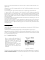
3.1 A/D Board Type Select Jumper
The CYEXP GP can be used with either DAS08 or DAS16 family boards because the signal
assignments of the 37-pin connectors match those of the DAS08 and may be adapted to those of
the DAS16 with a CBL MX10 cable. Select the A/D board type via the JB10 jumper.
Jumper JB10 on the, CYEXP GP located near the 37-pin connector, selects the
A/D board family as DAS08 or DAS16.
Figure 3-1 shows the jumper set to use the CYEXP GP with a CYDAS 8
family board.
'$6 '$6
Figure 3-1
DAS Family Select
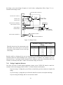
3.2 Setting The Output Channel
Jumpers labeled “CH SEL” located near the 37-pin connector select the A/D board channel that the
output from the active sensor will be connected to.
OUTPUT CHANNEL
SELECT JUMPER
37
0
36
1
35
2
34
3
33
4
32
5
31
6
30
7
18
8
17
9
16
10
15
11
14
12
13
13
12
14
11
15
9
8
7
INPUT 0
AMP
GAIN
1 OR 2.5
8-CHANNEL MULTIPLEXER
37-Pin
CONNECTORS
INPUT 1
INPUT 2
INPUT 3
INPUT 4
INPUT 5
INPUT 6
INPUT 7
MUX ADDR 3
MUX ADDR 2
MUX ADDR 1
P1 & P2
Figure 3-2. Output Channel Select Jumper
5
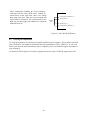
There are three groups of 16-position jumpers. One jumper group determines the signal output channel,
one jumper group determines the excitation voltage output channel and one determines the Cold Junction
Compensation (CJC) output channel. Signal output is always used, CJC output is used only with
thermocouples and excitation output may be used with bridge sensors.
There are 16 jumper locations for each function. Each corresponds to one of the 16 pins on the 37 pin
connector. When the CYEXP GP is connected to a DAS08, only the first 8 channels (labeled 0-7) can
be used. When the CYEXP GP is connected to a DAS16, all 16 jumper positions can be used. In each
case, the jumper corresponds to a channel number on the A/D board.
If the jumper setting does not agree with the selection made in InstaCal setup, InstaCal and the Universal
Library will not be able to make readings from the CYEXP GP. Figure 3-3 is a diagram of the Channel
Select jumper. There are two other groups of output jumpers similar to this group.
The top group (shown here) is marked CH SEL
(Channel Select), the center jumper group is
VEXC SEL (excitation voltage select) and the
bottom group is marked CJC SEL (Cold Junction
Compensation Select).
0 1 2 3 4 5 6 7
8 9 10 11 12 13 14 15
CH SEL
CHANNEL 0 SELECTED
FOR SENSOR OUTPUT
Figure 3-3. Output Channel Select Jumper
Place the jumper on the pin which corresponds to the A/D board's input channel. Each jumper set must
select a unique A/D channel. For example, if you are using the excitation or CJC outputs in addition to
the signal output, each should be set to a different channel number.
One individual channel must be selected for each bank of 8 EXP channels. For example, if you are using
several CYEXP GP boards, the jumper setting for each board must be unique. If you select channel 0
for the first board, do not use this channel for any of the other boards.
3.3 Configuring the A/D Board
3.3.1
DAS08 Family Setup
The input mode of the A/D board must be single-ended to be compatible with the CYEXP outputs.
Some of the boards in the DAS08 series have differential inputs that can be converted to single-ended
inputs. See the information shipped with your A/D board for conversion to single-ended inputs.
3.3.2
DAS16 Family Setup
The input mode of the A/D board must be single-ended to be compatible with the CYEXP outputs.
Most of the DAS16 series is switch selectable for either 8 differential or 16 single ended inputs. When
used with the CYEXP, set the switch to 16 channel, single-ended mode.
3.3.3
All A/D Boards
If you are using an A/D board with switch - selectable ranges, consider the application and determine the
best fit for range vs. expected voltage. For example, when measuring resistance such that the output of
the EXP board is expected to be in the range of 3 to 4.5 volts, a unipolar 5V range would be the best
choice.
6
If the range on your A/D board is fully programmable, the software you use for measurement will
determine the range.
3.4 CONNECTING THE CYEXP GP TO THE A/D BOARD
3.4.1
Connecting to a DAS08 Series A/D Board
A CYDAS 8 series board may be connected directly through a CBL 3700 series cable from the P1
connector on the CYEXP GP to the A/D analog connector. The JB10 jumper should be left in the
DAS08 position as set at the factory.
3.4.2
Connecting to a DAS16 Series A/D Board
Connection to a DAS16 series board requires a special 37-conductor cable (CBL MX10) since pin
relationship of CYEXP and DAS16 signals is not 1:1.
Install the CBL MX10 cable connector labeled “MUX” into the P1 connector of the CYEXP GP
board and the other end into the DAS16 series board’s analog connector.
3.4.3
Other A/D Boards
For other boards, use the connector diagram in
Figure 3-4 to construct a cable, or call us and
discuss the possibility of a custom
manufactured cable.
DAS16 LLGND
19
OUTPUT 8 / LLGND
18
OUTPUT 9
The signals from the CYEXP GP are
voltages from each channel and an analog
ground. There should be no voltage between
the analog ground and the power ground.
The MUX address lines control the setting of
the channel multiplexer. When all are low, the
mux is set to channel 0. The lines are binary
coded. MUXADDR1 is the LSB and
MUXADDR3 is the MSB.
OUTPUT 10
OUTPUT 11
OUTPUT 12
OUTPUT 13
OUTPUT 14
OUTPUT 15
SHUNT CALIBRATION
MUX ADDR 3
MUX ADDR 2
MUX ADDR 1
NC
A jumper (CH SEL) selects which output
channel is read by the DAS08 or DAS16
board.
NC
NC
NC
NC
NC
17
16
15
14
13
12
11
10
9
8
7
6
5
4
3
2
1
37
OUTPUT 0
36
OUTPUT 1
35
OUTPUT 2
34
OUTPUT 3
33
OUTPUT 4
32
OUTPUT 5
31
OUTPUT 6
30
OUTPUT 7
29
+5 VOLTS FROM PC
28
POWER GROUND
27
NC
26
NC
25
NC
24
NC
23
NC
22
NC
21
NC
20
NC
Figure 3-4. 37-Pin Connectors
7
3.5 Powering The CYEXP GP
The CYEXP GP can be powered through the 37-pin cable, the power screw terminal or the Molex
connector. The power that can be carried through the 37-pin connector is limited so we recommend
using this source only when a single CYEXP GP is used.
The power required to run a CYEXP GP is dependent on the board configuration. Remember that
additional power will be drawn when the CYEXP GP is configured for resistance measurement (bridge
configuration) due to the current required for each bridge.
3.5.1
Power Source Switch
X1
REM
One of the switches on the eight-position DIP switch (S17) near
the output channel jumpers controls the source of the +5 volts
power to the board. Shown in Figure 3-5 it is the 3rd switch
from the left.
When positioned down, (ON, +5 COMP), the +5V power is
drawn from the personal computer through the signal cable.
S17
0.5V
1V
2V
4V
10V
+5 COMP
X2.5
GND
When positioned up (OFF, REM) , +5V power is taken from
the optional external 5V power connector (the Molex connector
labeled P19) or the +5V screw terminal connection.
Figure 3-5. Power Source Switch
3.5.2
Powering with the 37-Pin Connector
You can power the CYEXP GP via the 37-pin cable. No more than one CYEXP GP should be
powered using the 37-pin cable.
This option is not available when using some A/D boards. If the A/D board you are using supplies +5V
at pin 29 (or at pin 1 when using the CBL MX10 signal cable), you can power the CYEXP GP
through the 37-pin connector by setting the power select switch on S17 to “+5 COMP.”
3.5.3
Powering with the Molex Connector
The CYEXP GP can be powered off the PC's power supply by connecting the optional external 5V
power connector (the Molex connector labeled P19) to the PC’s power supply through a C-MOLEX-10
cable. This cable has the same Molex connector that is used inside the PC and so can be connected
directly to the PC's power supply through one of the spare connectors. The cable is keyed, so it should
not be forced. When inserted properly it will slide easily and snap in place.
3.5.4
Powering Through the Power Screw Terminals:
A set of screw terminals labeled “+5V REM” and “REM GND” are located below the 37-pin connectors
P1 and P2. You can power the CYEXP GP from a +5V (±5%) power supply capable of at least 400
mA. For this option, set the power select switch on S17 to “REM.”
CAUTION: Connect the ground of the power supply to the ground of the personal computer with a
heavy gauge wire. If you do not strap the two grounds together, a voltage between these grounds will
8
affect measurements. If the potential exceeds the protection range of the input circuits, the board may be
damaged.
At this time, ignore the other screw terminals located next to the power and ground terminals. They are
needed only with certain sensors and will be explained in those sections.
3.6 Daisy-Chaining CYEXP GP Boards
Connect one CYEXP GP to another using a CBL 370x ribbon cable. Connect from P2 on the ‘upstream’
board to P1 on the ‘downstream’ board. Make sure each of the boards in the chain have a unique channel
selected (CH SEL jumper is set to a different number on each board).
3.7 Connecting a Test Voltage
(+)IEXC
+ SENSE
+EXCITATION CURRENT
+ VOLTS IN
+ SENSE
−P
(−)IEXC
+ VOLTS IN
SHORTING WIRE INSTALLED
− SENSE
−SENSE
+P
There is not enough room on the board for the full name
next to each terminal so the eight screw terminals
associated with each input circuit are labeled on the
CYEXP GP as follows:
−EXCITATION CURRENT
+SENSE Connect to + voltage
−SENSE Jumper to −P
−P
Connect to Ground
− VOLTS IN OR COMMON
To connect a voltage signal to the input circuit you use
three screw terminals as follows:
EXCITATION. VOLTS
Each input circuit has eight screw terminals associated
with it. These terminals are shown in the diagram to the
right.
+P
Make your initial test of the CYEXP GP with a voltage
signal of between -5 and 5V. If you use an AC signal
source, keep the frequency below 70 Hz to avoid
attenuation by the CYEXP GP’s low pass filter.
CH0
Figure 3-6. Input Screw Terminals
+P
−SENSE
−SENSE
−IEXC
−P
+SENSE
+SENSE
+IEXC
Excitation voltage
Low side of input
Hardwired to the other −SENSE, same function
Excitation current return
Excitation voltage return, common with −IEXC
High side of input
Hardwired to other +SENSE, same function
Excitation current
The use of the terminals is dependent on the type of sensor you have connected to the input circuit, and
the nomenclature on the terminals has been chosen to make the most sense for bridge and RTD sensors.
For voltage and thermocouple sensors the names on the terminals are not typical. Please refer to the
section on the measurement you are making in order to learn how to use the terminals.
9
3.8 Verifying the Installation
For verification of the installation, leave any switches or jumpers not mentioned above in their default
positions. Each of the gain switches (CH0 through CH7 and S17-7) should be off (toward the upper edge
of the board) for a gain of X1 (unity gain). The channel configuration switches (labeled “IN CONFIG”
should be left in the default position (the switches labeled “4” in the ON position and those labeled “3”
in the OFF position - the label is printed on the board, not the switch).
To verify the installation, use the InstaCal program installed on your computer. This software came with
your A/D board if you bought the board from the same manufacturer as the CYEXP GP. If your A/D
board is not from the same manufacturer but is compatible, please call technical support and request a
copy of InstaCal.
Use InstaCal's TEST option to verify that a signal present at one of the CYEXP GP inputs can be read.
You will not need to set any jumpers other than those previously mentioned, and should not set any
switches or install any passive components until you have verified the installation.
When using an AC signal source, keep the frequency below 70 Hz to avoid attenuation by the low pass
filter.
10
4
CONFIGURATION FOR VOLTAGE MEASUREMENT
The CYEXP GP is an amplification, signal conditioning and multiplexing accessory for DAS boards.
The inputs are suitable for connecting a low frequency voltage to the DAS board so it can be measured.
The CYEXP GP is a one-of-eight multiplexer which means that for every channel in your DAS board,
you can multiplex eight different signals to it. You can expand the number of inputs of your DAS board
by eight for every CYEXP GP board, up to the number of inputs on the DAS board. For example,
a DAS08 has 8 inputs. Eight times eight is sixty-four. Using CYEXP GP boards you can bring 64 inputs
into the PC with one DAS08 in one slot.
It is unlikely that you purchase a CYEXP GP to measure voltages. The CYEXP GP has a 70Hz low
pass filter and quite a bit of elaborate circuitry designed for bridges, TCs, and RTD sensors. For
applications requiring only voltage measurements, a CYEXP 16 or CYEXP 32 would be less expensive
and do the same job.
Possibly you have one or two voltages to measure in addition to bridge or RTD sensors and would like to
connect those signals to the CYEXP GP.
4.1 Channel Selection
The General Configuration section describes the channel selection, setting the jumper and verifying the
installation and operation of the CYEXP GP with your data acquisition board. Configure your boards
as described in that section before continuing with this section.
4.2 Powering the CYEXP GP
The General Configuration section describes the power selection options, setting the power select switch
and verifying the installation and operation of the CYEXP GP with your data acquisition board.
Configure your boards as described in that section before continuing with this section.
4.3 Determining The Appropriate Gain
To accurately measure a voltage, the full scale of the signal should be matched to the full range of the
input circuit. (Most DAS boards have an input range of ±5V, which is the native range of the analog to
digital converter at the heart of the board. Some DAS boards include amplification on the input circuit to
allow the signal to be amplified to make better use of the resolution of the A/D.) For example, an input
signal which varies between 0 and 1 volt would only be using 1/10th of a ±5V A/D converter's
resolution. By switching the input signal of the DAS board to unipolar (no negative voltage) and
amplifying the input signal by 5, the entire range of the A/D converter is used and a higher resolution
measurement may be made. By adding this gain and selecting this range, the resolution on a 12-bit A/D
improves from 2.4 millivolts per bit to 0.24 millivolts per bit. If you needed to measure a change of 1
millivolt, you would need an amplification of 10.
In order to match your signals with the input range of the A/D board, you should do a similar calculation
and set switches on the CYEXP GP for the required gain. Remember to make sure that the settings in
InstaCal match the switches on the DAS and CYEXP GP boards.
If you are measuring signals greater than the maximum full scale range of the A/D, see the section on
attenuation.
11
To choose a switch-selectable amplification, here are the calculations you need to perform:
Divide the full range selected for the A/D board by the full range of the signal to be measured to
determine the maximum gain of the CYEXP board. For best resolution, use the highest gain possible
up to the calculated maximum gain.
For example, if the A/D board is to be used at a range of ±5V, the full range of the board is 10. If your
signal ranges between -0.5 volts and 0.5 volts, the full range of the signal is 1 volt. Divide 10 by 1 for a
result of 10. That is the maximum gain you can use.
If your signal is unipolar and ranges less than 0 to 5V, you would likely choose the 5V unipolar range for
the A/D board (if available). Given an input signal ranging from 0 to 0.5 volts, the full range of the
signal is 1/2 volt. Divide 5 (the full range of the A/D) by 0.5 (the full range of the signal for a result of
10. That is the maximum gain you can use.
4.4 Setting the Gain
Gain (amplification) allows you to boost your signal to take full advantage of the resolution of the A/D
converter. However, when amplifying a signal, any noise is amplified as well.
Amplification for ALL channels (board output gain) is switch selectable (S17) for X1 or X2.5.
Input amplification for EACH CHANNEL is switch selectable (GAIN switches CH0 through CH7) for
X1, X10, X100 or X1000. A user-specified gain may be set by supplying a precision resistor at position
RX### and setting the “U” option on the CH ## GAIN switch to ON.
4.4.1
Setting Board Gain
REM
X1
There is a switch on DIP switch block S17
labeled X1 and X2.5. Sliding this switch down
amplifies the output of the multiplexers by 2.5.
The factory default position (up) has a gain of 1
(unity). Refer to Figure 4-1.
S17
0.5V
1V
2V
10V
4V
X2.5
+5 COMP
GND
The X2.5 gain switch is useful in some voltage
and bridge measurements. If you desire a
voltage gain of 2.5, 25, 250 or 2500, set this
switch down.
Figure 4-1. Board Output Gain Switch Location
For voltage measurements, a gain of 2500 is very high and will reduce your signal to noise ratio.
The effect of this switch is multiplicative with respect to the individual channel gains. For example, if
you have set an input channel gain to X100 and the board output gain to X2.5, the signal is amplified by
250 before it reaches the A/D board.
12
4.4.2
Setting Channel Gain
Select a gain (higher than unity) by moving the switch for
that gain down. All other switches should be left in the
UP position.
N
O
X1000
X100
X10
on the CYEXP GP by
and setting the switch
position. See Table 4-1
and some sample gain
U
A custom gain may be selected
installing a precision resistor
marked “U” (User) in the down
following for board positions
values.
CH4
GAIN FOR CHANNELS 0 and 4
SET FOR A GAIN OF 10.
SLIDER DOWN SELECTS GAIN
ALL OTHERS TO BE OFF (UP)
N
O
CH0
Figure 4-2. Input Channel Gain Select Switches
Channel
0
1
2
3
Table 4-1. Resistor Positions for User-Selected Gains
Resistor Position
Channel
Resistor Position
RX100
4
RX104
RX101
5
RX105
RX102
6
RX106
RX103
7
RX107
Gain
50
100
200
500
700
800
Resistor Value
776 Ohms
364 Ohms
161 Ohms
40 Ohms
17 Ohms
10 Ohms
The equation for selecting the USER gain resistor is:
RUSER= [40000 / (Gain − 1)] − 40
Amplifying a signal on one channel will not affect the reading on another channel.
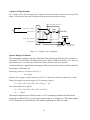
4.5 Attenuation
If your signal is in a range greater than the full scale range of the A/D, you must either set the A/D for a
higher full scale range (if available) or divide (attenuate) the signal until the result is less than or equal to
the A/D’s full scale range. This section describes signal attenuation.
13
INPUT
A voltage divider is constructed from a pair of
precision resistors selected according to the
equation:
Ra
OUT
Volts In
Attenuation = (Ra + Rb) / Rb
See Figure 4-3 at right for the schematic of
a voltage divider.
Volts Divided
Rb
PC GROUND
PC GROUND
Figure 4-3. Voltage Divider
For example, if your signal is 0 to 10V, it must be attenuated to 5V max. for an attenuation
of 2:1 or simply 2.
Using 10k resistors: 2 = (10K + 10K) /10K.
For any attenuation, pick a suitable resistor for Rb. Then use this formula to calculate Ra:
Ra = (A−1) x Rb
You will need to construct the voltage divider remote from the CYEXP GP board.
4.6 Setting the Input Configuration
CH4
Channel Configuration Switch - Voltages
3
4
3
IN CONFIG
3
4
3
4
For voltage measurements on a particular channel, set the
switches labeled “4” to the ON (down) position for that
channel.
N
O
4
A channel configuration switch is associated with each
channel (Figure 4-5). The switches are used to configure the
input circuits for voltage inputs, thermocouple inputs, 2, 3, or
4-wire RTDs and bridges.
N
O
Set the switches labeled “3” in the OFF (up) position.
CH0
CHANNEL CONFIGURATION SWITCHES SET
VOLTAGE, THERMOCOUPLES, OR 2/4-WIRE RTDs
BOTH 4s ARE ON (DOWN), BOTH 3s ARE OFF (UP)
Figure 4-5. Channel Configuration Switches
4.7 Connecting Voltage Signals
Voltage signals can be single ended or differential, and the full scale may have to be matched to the range
of the CYEXP GP and DAS board combination via amplification or attenuation. To connect a voltage
and make an accurate measurement, each of these issues must be addressed (see section 4.3).
14
+ VOLTS IN
+ SENSE
+ SENSE
+EXCITATION CURRENT
+ VOLTS IN
SHORTING WIRE INSTALLED
−P
−EXCITATION CURRENT
−SENSE Signal low, or CH LO on a DAS board.
Must be jumpered to −P for single-ended
− VOLTS IN OR COMMON
+SENSE Signal high, or CH HI on a DAS board
EXCITATION. VOLTS
To connect a voltage signal to the input circuit you
need only use three screw terminals. These are:
+P
Each input circuit has eight screw terminals associated
with it. These terminals are shown in Figure 4-4 to the
right.
Low Level Ground (LLGND)
(+)IEXC
−P
(−)IEXC
− SENSE
−SENSE
+P
CH0
Figure 4-4. Input Screw Terminals
4.7.1
Single-Ended Inputs
A single-ended input has two wires connected to the CYEXP GP; a signal high and a Low Level
Ground (LLGND). The LLGND signal must be the same ground the PC is on. Single-ended mode is
selected by installing a jumper between the signal low (−SENSE) and ground (−P). The -SENSE
terminal is then connected to the signal ground and the +SENSE terminal is connected to the signal.
4.7.2
Floating Differential
A floating differential input has two wires from the signal source and a 10K ground reference resistor
installed at the CYEXP GP input. The two signals from the signal source are Signal High and Signal
Low. The reference resistor is connected between the CYEXP GP “−SENSE” and “-P” pins and the
Signal Low is connected to the -SENSE terminal. The +SENSE terminal is connected to the Signal High.
A floating differential hookup is handy when the signal source is floating with respect to ground, such as
a battery. The floating differential input will reject up to 10V of EMI energy on the signal wires.
CAUTION: Is the signal source really floating? Check it with a voltmeter before risking
the CYEXP GP and the PC.
4.7.3
Fully Differential
A differential signal has three wires from the signal source. The signals are Signal High, Signal Low and
Signal Ground (LLGND). Signal High is connected to the +SENSE terminal and Signal Low is
connected to the -SENSE terminal. The ground reference must be connected to the -P terminal.
A differential connection allows you to connect the CYEXP GP to a signal source with a ground that is
different than the PC ground, but less than 10V difference, and still make a true measurement of the
signal. For example, a laboratory instrument with its own wall plug. Sometimes there is a voltage
between wall outlet grounds.
15
4.8 Verifying the Installation
To verify the installation, use the InstaCal program installed on your computer. This software came with
your A/D board if you bought the board from the same manufacturer as the CYEXP GP. If your A/D
board is not from the same manufacturer but is compatible, please call technical support and request a
copy of InstaCal.
Use InstaCal's TEST option to verify that a signal present at one of the CYEXP GP inputs can be read.
When using an AC signal source, keep the frequency below 70 Hz to avoid attenuation by the low pass
filter.
16
5
CONFIGURATION FOR THERMOCOUPLE MEASUREMENT
Thermocouples are temperature sensors constructed of wires of two dissimilar metals fused together at a
point. This junction of two metals produces a voltage that varies relative to temperature. Thermocouple
voltages require several manipulations in order to be useful. These are:
1. A very low voltage is produced and so must be amplified by a factor of between 100 and 1,000.
2. The voltage produced by the thermocouple is not linear with respect to temperature, so it must be
linearized. Linearization in this case is calculated by software after the voltage is acquired.
3. A voltage-producing junction is also created at the screw terminal where the thermocouple is
connected to the CCYEXP GP. The temperature at this “cold junction” must be measured and the
voltage calculated and subtracted from the total measured from the thermocouple. This is also calculated
by software. The circuit that measures this temperature is the Cold Junction Compensation (CJC) circuit.
4. Thermocouples are subject to EMI and RFI noise due to the very low level of the voltage and the large
amplification factor. These affects can be reduced through averaging and filtering. There is a 70Hz low
pass filter on the CYEXP GP. Averaging may be done in software.
Thermocouples are not as accurate as RTDs or other precision temperature sensors, but they are much
less expensive. Sometimes, an attempt is made to make a measurement beyond the accuracy of the
thermocouple such as measuring 1/10th of a degree over the full scale. Read the accuracy and
repeatability specification of the thermocouple, and consider the effects of linearization on the reading
before choosing thermocouples.
The CYEXP GP is not the optimum choice for thermocouple-only applications. The CYEXP 32 and
CYEXP 16 are less expensive and just as accurate for thermocouple measurements. The CYEXP GP has
extra circuitry devoted to bridge and RTD sensors.
5.1 Selecting The Output Channel
The General Configuration section describes the channel selection, setting the jumper and verifying the
installation and operation of the CYEXP GP with your data acquisition board. Configure your boards
as described in that section before continuing with this section.
5.2 Selecting The CJC Output Channel
There is a set of jumpers near the 37-pin connectors labeled “CJC SEL,” which stands for cold junction
compensation select. These jumpers connect the on-board measurement of the cold junction temperature
to one of the A/D board channels for use in temperature calculations.
The CJC temperature reference is universally used by software to compensate for the voltage induced at
the cold junction (the screw terminal). The software package you are using will determine which channel
you need to set this jumper on. The default is channel 7 (the channel used by default by the Universal
Library). If you are not using the Universal Library, check your software documentation before selecting
a channel. Failure to supply the CJC reference by installing the jumper on the correct channel will result
in inaccurate temperature calculations by the software.
17
The jumper for the CJC channel select (Figure 5-1)
looks just like the jumper for output channel
selection.
0 1 2 3 4 5 6 7
8 9 10 11 12 13 14 15
CJC SEL
CHANNEL 4 SELECTED
FOR COLD JUNCTION SENSOR OUTPUT
Set this jumper according to the instructions for the
software package you are using.
Figure 5-1. CJC Channel Select Jumper Pad
The CJC uses one analog input channel of the A/D board. The channel selected must be unique (the CJC
SEL jumper must not be set to the same number as that for CH SEL jumper or VEXC SEL jumper on this
board or any other EXP board that may be daisy-chained to this board).
5.3 Input Configuration
For thermocouple measurement, the channel input configuration switches must be set for two wire
measurement. Also, a ground reference should be established and open thermocouple detection should
be enabled. These options are selected by setting some switches and closing some solder pads on the
underside of the CYEXP GP.
5.3.1
Setting the Input Configuration
A channel configuration switch is associated with each
channel. The switch is used to configure the input circuit
for two or four wire measurements. When measuring
thermocouples, two wire measurement should be used.
CH4
N
O
3
4
3
4
Set the two switches labeled “4” on each IN CONFIG
Channel Configuration switch to the ON (down) position for
each channel used for thermocouple measurement. (See
Figure 5-2 on the right.)
IN CONFIG
3
4
3
4
Set the two switches labeled “3” on each IN CONFIG switch
for thermocouple channels to the OFF (up) position.
N
O
CH0
CHANNEL CONFIGURATION SWITCH SET FOR THERMOCOUPLES
BOTH 4s ARE ON (DOWN), BOTH 3s ARE OFF (UP)
Figure 5-2. Channel Configuration Switches
5.3.2
Enabling Open Thermocouple Detection (OTD)
Open thermocouple detection (OTD) is enabled for a channel by installing a resistor and closing the 'TC'
pad with a solder bridge (see Figures 5-3 and 5-4). There are locations marked “TC” for each channel for
this purpose.
OTD provides the high side of the thermocouple signal with a reference to −50mVDC at very low
current. If a thermocouple opens, it ceases to produce a voltage. If that happens, the OTD voltage drives
the signal on that channel to full minus. Most software is set up to alarm for an open thermocouple when
a temperature falls to full scale minus value. The CYEXP GP will accurately measure thermocouples
without the 'TC' pad closed but you must close it and install a 100K resistor to have OTD.
18
Channel 0 RX 5
Channel 1 RX11
Table 5-1. 100K ohm Resistors to be Installed for OTD:
Channel 2 RX 17
Channel 4 RX 29
Channel 6 RX41
Channel 3 RX 23
Channel 5
RX 35
Channel 7 RX47
Please solder the pads with the solder provided. It has a water soluble flux which should be washed off.
If you use another type of solder or do not wash off the flux it may affect your readings.
EXCITATION VOLAGE (+)
EXCITATION. VOLTS (+)
- THERMOCOUPLE LEAD SENSE LOW (-)
SENSE LOW (-)
EXCITATION CURRENT (-)
GAIN SW
EXCITATION VOLTS (-)
+ THERMOCOUPLE LEAD SENSE HIGH (+)
AMP
SENSE HIGH (+)
80Hz Low
Pass Filter
TO CHANNEL
MULTIPLEXOR
100K
-TC PULL
50 mV
EXCITATION CURRENT (+)
10K
GND REF
Figure 5-3. OTD and Ground Reference Jumper Pads - Schematic
NOTE: If you want to change the use of the input circuit to an RTD or bridge sensor, remove the solder
that closes the TC pad (and the G pad also).
Figure 5-4. OTD and Ground Reference Jumper Pads - Locations (Typ.)
19
5.3.3
Adding a Ground Reference
The CYEXP GP inputs are fully differential which helps reject noise on thermocouple wires. If
thermocouples connected to the CYEXP GP inputs are to work properly, the 'G' pad must be closed on
any channel used for thermocouple measurement (see Figures 5-3 and 5-4). The 'G' pad provides a
reference from ground to the analog low input via a 10K resistor. Only enough current passes through
the resistor to provide a reference to ground. The analog high and low inputs are still able to float within
the common mode range.
NOTE: If you want to change the use of the input circuit to an RTD or bridge sensor, remove the solder
that closes the G pad (and the TC pad also).
5.4 Determining the Appropriate Gain
The voltage from a thermocouple must be amplified in order to take advantage of the A/D board's full
resolution. Without amplification, you would not get much resolution from thermocouples, as you can
see in the tables below. Typical gain settings for use with thermocouples are between X10 and X250.
Tables 5-3 and 5-4 below may be used to help determine the appropriate gain to use for the temperature
range and thermocouple type in use.
Type
J
K
T
E
S
R
Table 5-3. Resolution vs Thermocouple Gain Settings for a ±5V, 12 bit A/D
Output
Min °C
Max °C
°C/bit
°C/bit
°C/bit
µV/°C
@X10
@X100
@X250
51
0
750
4.78
0.48
0.19
40
-200
1,250
6.1
0.61
0.24
350
6.1
0.61
0.24
40
−200
900
3
0.39
0.16
62
−200
7
0
1,450
34.9
3.49
1.4
7
0
1,450
34.9
3.49
1.4
°C/bit
@X1000
0.04
0.06
0.06
0.03
0.35
0.35
A J-type thermocouple outputs 51mV per degree centigrade at 20°C. At a gain of 100, a 12 bit A/D on
the ±5V range resolves to 0.00002442 volts per bit (24.42µV/bit).With an output of 51mV/°C, that
represents about 0.5°C/bit. Look under the gain of 100 for a J-type and you will find 0.48°C/bit.
The table below shows the thermocouple output voltage at maximum temperature amplified by four
possible gain values. Where the output voltage exceeds 5V, the reading is clipped.
Type
J
K
T
E
S
R
Table 5-4. Voltage Output @ Maximum Temperature
Output
Max °C
Vout at Max Temp
@Max
X10
X100
X250
Temp
42.3mV
750
0.42
4.2
10.6
50.6mV
1,250
0.51
5.1
12.7
17.8mV
350
0.18
1.8
4.5
68.8
900
0.69
6.9
17.2
15mV
1,450
0.15
1.5
3.8
16.7
1,450
0.17
1.7
4.2
20
X1000
42
51
18
69
15
17
Voltages which exceed the ±5V range are in bold italics in the table above. Table 5-5 shows the
temperature at which the reading is clipped (the maximum readable temperature for thermocouple types
at a given gain).
Table 5-5. Maximum Readable Temperatures with A/D on ±5V Range
Type
Max °C
Max Readable Temp vs Gain
X10
X100
X250
X1000
J
750
750°C
750 °C
366°C
95°C
K
1,250
1,250°C
1,232°C
484°C
121°C
T
350
350°C
350°C
350°C
115°C
E
900
900°C
660°C
287°C
80°C
S
1,450
1,450°C
1,450°C
1,450°C
576°C
R
1,450
1,450°C
1,450°C
1,450°C
548°C
From these tables, you can determine that if you want to use a J-type thermocouple to make a reading of
700 degrees, the gain should be set at 100. This yields a resolution of 0.48 degrees C per bit.
5.5 Setting the Gain
Once you have determined the gain required for your application, set the gain of the CYEXP GP using
the following guide.
Amplification for ALL channels (board output gain) is switch selectable (S17) for X1 or X2.5.
Input amplification for EACH CHANNEL is switch selectable (CH0 through CH7) for X1, X10, X100 or
X1000. A user-specified gain may be set by supplying a precision resistor at position RX### and setting
the “U” option on switch CH ## to ON.
5.5.1
Setting the Board Gain
Output Gain Switch
REM
S17
0.5V
1V
2V
10V
4V
X2.5
+5 COMP
GND
The X2.5 gain switch is useful in some thermocouple
measurements. If you desire a voltage gain of 2.5, 25 or 250, set
this switch down. Recommended gains for thermocouples are
between X10 and X200.
X1
There is a switch on DIP switch block S17 (Figure 5-5) labeled
X1 and X2.5. Sliding this switch down amplifies the output of
the multiplexers by 2.5. The factory default position (up) has a
gain of 1 (unity).
Figure 5-5. Output Gain Switch Location
The effect of this switch is multiplicative with respect to the individual channel gains. For example, if
you have set an input channel gain to X100 and the board output gain to X2.5, the signal is amplified by
250 before it reaches the A/D board.
5.5.2
Setting the Channel Gain
21
There is a gain switch for each channel (Figure 5-6). Set the input channel gain to match the expected
voltage output of the bridge you are measuring to the input range of the A/D board as described above.
Channel Gain Switches
There is a set of DIP gain switches for each input
circuit labeled GAIN (Figure 5-6). There are four,
two-position switches for each channel. The gain
switches are labeled U, X10, X100, and X1000.
N
O
A custom gain may be selected on the CYEXP GP
by installing a precision resistor and setting the
switch marked “U” (User) in the down position. See
Table 5-2 below for positions and some sample gain
values.
X1000
X100
X10
U
Select a gain (higher than unity) by moving the
switch for that gain down. All other switches should
be left in the UP position.
CH4
GAIN FOR CHANNELS 0 and 4
SET FOR A GAIN OF 10.
SLIDER DOWN SELECTS GAIN
ALL OTHERS TO BE OFF (UP)
N
O
CH0
Figure 5-6. Channel Gain Switches
Channel
0
1
2
3
Table 5-2. User Gain Resistors - Identities
Resistor Position
Channel
Resistor Position
RX100
4
RX104
RX101
5
RX105
RX102
6
RX106
RX103
7
RX107
Gain
50
100
200
500
700
800
Resistor Value
776 Ohms
364 Ohms
161 Ohms
40 Ohms
17 Ohms
10 Ohms
The equation for selecting the gain resistor is:
RUSER = (40000 / (Gain − 1) ) − 40
5.6 Verifying the Installation
Your channel is now configured to make thermocouple measurements. To verify the installation, use the
InstaCal program installed on your computer. This software came with your A/D board if you bought the
board from the same manufacturer as the CYEXP GP. Use the CALIBRATE option to calibrate the
CJC and verify the operation of the channel. Use the TEST option to make a measurement in
engineering units.
22
6
CONFIGURATION FOR RTD MEASUREMENTS
An RTD is a temperature sensor that consist of a resistive element, usually a length of wire encased in a
sheath. Various wire materials are used with platinum being the most common. There are three types of
hookups: two-wire, three-wire, and four-wire. An excellent source of information on RTDs and how to
select one for your application may be found in the OMEGA Engineering catalog.
6.1 Channel Selection
The General Configuration section describes the channel selection, setting the jumper and verifying the
installation and operation of the CYEXP GP with your data acquisition board. Configure your boards
as described in that section before continuing with this section.
6.2 VEXC JUMPER Select
There is a set of jumpers near the 37-pin connectors labeled “VEXC SEL,” which stands for channel
excitation voltage select. These jumpers connect the on-board excitation voltage to one of the A/D board
channels so that it may be measured. CyberResearch does not use a measurement of the excitation
voltage in any of its software. You do not need to set this jumper if you are using the CYEXP GP
with CyberResearch software, or with packages such as Labtech Notebook™, which use the Universal
Library. Use this jumper only with software from other manufacturers that specifically
require it.
6.3 CJC Jumper Selection
There is a set of jumpers near the 37-pin connector labeled “CJC SEL,” which stands for cold junction
compensation select. Remove this jumper. There is no cold junction compensation used with bridge
sensors.
6.4 Powering the CYEXP GP
The General Configuration section describes the power selection options for powering the CYEXP GP
itself. Configure your boards as described in Powering the CYEXP GP in the General Configuration
section before continuing with this section.
6.5 Determining the Appropriate Gain
To accurately measure a voltage, the full scale of the signal should be matched to the full range of the
input circuit. (Most DAS boards have an input range of ±5V, which is the native range of the analog to
digital converter at the heart of the board. Some DAS boards include amplification on the input circuit to
allow the signal to be amplified to make better use of the resolution of the A/D.) For example, an input
signal which varies between 0 and 1 volt would only be using 1/10th of a ±5V A/D converter's
resolution. By switching the input signal of the DAS board to unipolar (no negative voltage) and
amplifying the sign wave signal by 5, the entire range of the A/D converter is used and a higher
resolution measurement may be made. By adding this gain and selecting this range, the resolution on a
23
12-bit A/D improves from 2.4 millivolts per bit to 0.24 millivolts per bit. If you needed to measure a
change of 1 millivolt, you would need an amplification of 10.
In order to match your signals with the input range of the A/D board, you should do a similar calculation
and set switches on the CYEXP GP for the required gain. Remember to make sure that the settings in
InstaCal match the switches on the DAS and CYEXP GP boards.
When using RTD’s, the expected output from the sensor should be calculated and the gain of the
CYEXP GP set accordingly.
To select the best gain for RTD type, base resistance and temperature range, consider that RTD
resistance changes with temperature, but the magnitude of the change also changes with temperature.
RTD type determines the ‘slope’ of the ohms vs. temperature curve. The most popular type has an
‘alpha’ of .00385, known as the European standard. Its value is .00385 ohms per ohm per °C.
The Universal Library and InstaCal support six different RTD types. Please call if you do not see the
RTD you are interested in listed here.
Material
‘Alpha’
Platinum
Platinum
Platinum
Copper
Nickel/Iron
Nickel/Iron
0.00392 American standard
0.00391
0.00385 European standard (Most popular, OMEGA’s standard also)
0.00427
0.00581
0.00527
To determine which gain to use, you must know the maximum temperature the RTD will be used to
measure, and thus the maximum resistance value of the RTD. Here is a table for platinum:
For 100 ohm RTD, alpha = .00385:
Temp (°C)
-200
-100
0
100
200
300
400
Resistance (ohms)
18.49
60.25
100.00
138.50
175.84
212.02
247.04
At a temperature of 400°C, the maximum resistance is 247.04 ohms
The equation for the voltage out of the CYEXP GP (the voltage your DAS board will convert into a
number) is:
VOUT = IEXC * RRTD * GAIN
Normally, the CYEXP GP supplies 1 mA of excitation current. The choices for standard gains are 1,
10, 25 and 100. (Higher gains are possible but are not generally practical for RTD applications.)
Thus, if you want to measure temperature in the range of -200 to 400°C with the RTD listed above,
the maximum voltage output would be:
V = 0.001 * 247.04 = 0.24704
24
If gain is set to X10, the DAS board will see 2.474 volts. This is ideal for a DAS board with a 2.5V
unipolar range.
If the gain were set to X25, the output would be 6.185 volts. The DAS board would have to be set in the
0 to 10 volt range.
If you are limiting your range of interest to -200 to 100°C, a common range, the calculations are:
V = 0.001 * 138.50 = 0.1385. Gain of 10 = 1.385V. Gain of 25 = 3.4625V. In this case, a gain of X25
and a DAS range of 0 to 10 volts would be best. A 12-bit A/D converter would be using 69% of its range
of 4096 counts, or a total of 2836 counts. The converter would be able to resolve to 0.035 degrees C.
That is more than enough converter resolution even though you are not using the full range of the DAS
board in this example.
If your DAS board has 16 bits of resolution, the DAS board would resolve to 0.0022 degrees. This is far
in excess of the accuracy of the RTD.
The stages of gain you choose are not only dependent on the RTD you choose, but on the range of
temperature you are measuring. Use the equation above to fine tune the CYEXP GP circuit to your
advantage, then be sure to update the InstaCal program so the Universal Library linearization routines
will operate properly.
6.6 Setting the Gain
Once you have determined the gain required for your application, set the gain of the CYEXP GP using
the following guide.
Amplification for ALL channels (board output gain) is switch selectable (S17) for X1 or X2.5.
Input amplification for EACH CHANNEL is switch selectable (CH0 through CH7) for X1, X10, X100 or
X1000. A user-specified gain may be set by supplying a precision resistor at position RX### and setting
the “U” option on switch CH ## to ON.
6.6.1
Setting the Board Gain
REM
X1
There is a switch on DIP switch block S17
(Figure 6-1) labeled X1 and X2.5. Sliding this
switch down amplifies the output of the
multiplexers by 2.5. The factory default
position (up) has a gain of 1 (unity).
S17
0.5V
1V
2V
10V
4V
X2.5
+5 COMP
GND
The X2.5 gain switch is useful in some voltage
and bridge measurements. If you desire a
voltage gain of 2.5, 25, 250 or 2500, set this
switch down.
Figure 6-1. Board Gain
The effect of this switch is multiplicative with respect to the individual channel gains. For example, if
you have set an input channel gain to X10 and the board output gain to X2.5, the signal is amplified by
25 before it reaches the A/D board.
25
6.6.2
Setting the Channel Gain
Channel Gain Switches
CH4
There is a set of gain switches for each input circuit
(Figure 6-2). There are two, 4-switch DIP blocks for
each channel. One is labeled “GAIN” and the other “IN
CONFIG.” The gain switches are labeled U (user), 10,
100, and 1000.
N
O
X1000
X100
The “U” switch and associated user resistor is of no
value to RTD measurement since the minimum specified
value produces a gain of X100, for which there is a
switch. A gain of X100 is the maximum you would use
with an RTD.
X10
U
Set the gain of your choice by placing a slide switch into
the ON (down) position.
GAIN FOR CHANNELS 0 and 4
SET FOR A GAIN OF 10.
SLIDER DOWN SELECTS GAIN
ALL OTHERS TO BE OFF (UP)
N
O
CH0
Figure 6-2. Channel Gain Switches
6.7 Input Configuration
RTDs may have 2, 3 or 4 wires coming from the probe. A switch labeled “IN CONFIG” must be set to
match the number of wires on your RTD. There is one switch per channel.
6.7.1
RTD Type
IN CONFIG Setting
2 Wire
3 Wire
4 Wire
4 & 4 ON, 3 & 3 OFF
3 & 3 ON, 4 & 4 OFF
4 & 4 ON, 3 & 3 OFF
Setting the Input Configuration
IN CONFIG
SET FOR 2- AND 4-WIRE RTDs
3
4
3
N
O
CH0
For three-wire RTDs, set both “3” switches ON
(down) and both “4” switches OFF (up).
IN CONFIG
4
Two- and four-wire RTDs share the same switch
position. Set both “4” switches ON (down) and
both “3” switches OFF (up).
3
4
3
4
A channel configuration switch is associated with
each channel. The switch is used to configure the
input circuit for 2, 3, or 4-wire RTDs (Figure 6-2).
N
O
CH0
SET FOR 3-WIRE RTDs
Figure 6-2. Channel Configuration Switches - RTDs
26
6.8 Connecting RTDs To Screw Terminals
The connections made to the screw terminal depend on the type of RTD you are using. The inputs of the
CYEXP GP are designed to provide the excitation and signal conditioning required for RTDs. An RTD
can have two, three, or four wires which you must connect to the CYEXP GP. This section shows the
three types of RTD connections and describes how to connect them to the input channels.
6.8.1
Two-Wire RTD Hookup
A two wire RTD has two leads, one to each side of the temperature sensitive resistor. The excitation
current is connected directly to the leads at the CYEXP GP screw terminals.
A two wire RTD is less accurate than the 4 wire
type, and so is not the first choice for the best
measurements. The reason for the inaccuracy is
that there is a slight resistance associated with the
excitation current flowing in the sense leads and
this resistance is added to the RTD’s resistance.
The inaccuracy is determined by the wire gauge
and length. However, as a general rule, the
difference in accuracy between the 2- and 4-wire
RTDs is often less than 0.1% of full scale.
CYEXP GP BOARD
2-WIRE
RTD
EXCITATION CURRENT (+)
SENSE HIGH (+)
SENSE LOW (-)
EXCITATION CURRENT (-)
Shorting Wires
Between Terminals
Figure 6-3. Two-wire RTD Hookup
6.8.2
Three-Wire RTD Hookup
A three wire RTD has three leads, one for each side of the temperature sensitive resistor and one for the
excitation current.
The current return and sense signals of one side
are shared. In the case of the CYEXP GP the shared 3-WIRE
signals are unconventional. The CYEXP GP is
RTD
a true clone of the original CYEXP GP, and
shares the unconventional circuit configuration,
which is corrected on the CYEXP RTD.
The unconventional configuration does not affect
the quality of the measurement but, if you
are familiar with RTDs and use a
standard connection, please be mindful of this difference.
Note: EXP-GP uses non-standard
3 wire RTD hookup
EXCITATION CURRENT (+)
SENSE HIGH (+)
SENSE LOW (-)
EXCITATION CURRENT (-)
Figure 6-4. Three-Wire RTD Hookup
6.8.3
Four-Wire RTD Hookup
A four wire RTD has four leads. One to each side of the temperature sensitive resistor and an excitation
current source and its return.
27
These connections eliminate the fixed inaccuracy
associated with the 2-wire RTD. Since virtually no
current flows on the sense lines, there is no voltage
drop in the sense lines. Thus, the error associated with
2-wire RTDs is eliminated. We recommend the 4-wire
RTD, but you must judge if the added cost is worth the
additional accuracy.
EXCITATION CURRENT (+)
SENSE HIGH (+)
4 WIRE
RTD
SENSE LOW (-)
EXCITATION CURRENT (-)
Figure 6-5. Four-Wire RTD Hookup
6.9 Verifying the Installation
To verify the installation, use the InstaCal program installed on your computer. This software came with
your A/D board if you bought the board from the same manufacturer as the CYEXP GP. If your A/D
board is not from the same manufacturer but is compatible, please call technical support and request a
copy of InstaCal.
Use InstaCal's TEST option to verify that a signal present at one of the CYEXP GP inputs can be read.
28
7
CONFIGURATION FOR RESISTANCE MEASUREMENTS
Resistance measurements are made using the CYEXP GP by constructing a resistor “bridge” containing
known resistor values that are to be compared to the resistor value to be measured. This is known as a
Wheatstone Bridge. The typical application is a strain gauge.
Strain gauge sensors are variable-resistance devices. When installed in one leg of the resistor bridge (as
the “unknown” resistor, their value can be measured. The Wheatstone Bridge circuit is extremely
sensitive to changes in resistance in one leg relative to the others. There are various types of bridge
sensors, but the descriptions and examples here are for strain gauges.
7.1 Channel Select
The General Configuration section describes the channel selection, setting the jumper and verifying the
installation and operation of the CYEXP GP with your data acquisition board. Configure your boards
as described in that section before continuing with this section.
7.2 VEXC Jumper Select
There is a set of jumpers near the 37 pin connector labeled “VEXC SEL,” which stands for channel
excitation voltage select. This jumper will connect the on board excitation voltage to one of the A/D
board channels so that it can be measured. CyberReseach does not use a measurement of the
excitation voltage in any of its software. You do not need to set this jumper if you are using the
board with CyberResearch software, or with packages such as Labtech Notebook™, which use
the Universal Library. Use this jumper only with software from other manufacturers that specifically
require it.
7.3 CJC Jumper Select
There is a set of jumpers near the 37-pin connector labeled “CJC SEL,” which stands for cold junction
compensation select. Remove this jumper. There is no cold junction compensation used with bridge
sensors.
7.4 Powering the CYEXP GP
There are two power issues to address. The first is the source of the 5 volt power to the board.
The second is the source of the bridge excitation voltage power.
7.4.1
Selecting the Power Source for the Board
The General Configuration section describes the power selection options for powering the CYEXP GP
itself. Configure your boards as described in Powering the CYEXP GP in the General Configuration
section before continuing with this section.
7.4.2
Selecting the Power Source for the Excitation Voltage
Bridge sensors consume a lot of power. In some cases the bridge sensors consume so much power that if
fully populated with eight sensors the on board excitation circuit would not have adequate power to
29
supply all eight sensors. This is an extreme case but is indicative of the attention you must pay to power
requirements when using bridge sensors.
Also, when selecting the power source for the excitation voltage, consider the voltage you will use for
excitation. The options available are 0.5, 1, 2, 4 and 10V. In general, higher excitation voltages are
better because a higher voltage increases the difference between the balance points of the bridge circuit,
which increases the accuracy of your measurement. The excitation voltage must be less than the source.
JB11
+P EXT
+12V
+5V
Jumper JB11 (Figure 7-1), located near the bottom edge of the board,
selects the source of the bridge excitation voltage. The three choices are
+5V (the same 5V source chosen for board power above), +12V (from the
PC through the 37-pin connector) or +PEXT (an external power supply
connected at the ±P EXT screw terminal).
Figure 7-1
Output Gain & Power Select
If you choose a separate power supply, it must be a floating, isolated supply (one with three terminals).
Do not tie the GND and −V terminal together. It must not exceed +15V.
The +5V and +12V jumpers are only valid with CYDAS 8 family boards. The +12V jumper is not
valid with the CYDAS 8-AO and -PGx. For more information on excitation voltages, refer to the
section on bridge sensors.
+5V Excitation Voltage Source
If your choice for the excitation voltage source is +5V, you may choose a 0.5V, 1V, 2V or 4V excitation
voltage for your bridge sensors. The +5V option is always available, since +5V is required to power the
CYEXP GP.
+12V Excitation Voltage Source
If your choice for the excitation voltage source is +12V PC power, you have the choice of 0.5, 1, 2, 4, or
10 volt excitation for your bridge sensors. The option to power from the PC 12 volt supply exists only
with DAS08 family boards, except that +12V is not valid with the CYDAS 8-AO or PGA.
+PEXT Excitation Voltage Source
An external power supply can be used. If you choose a separate power supply, it must be a floating, or
isolated supply (one with three terminals). Do not tie the GND and -V terminal together). Output voltage
must not exceed +15V. If your power supply is not floating, it is likely that you will create a ground loop
(current flow in the ground lines). A ground loop will induce an error in your reading. Connect the
power supply to the CYEXP GP at the terminals labeled −PEXT and +PEXT on the screw terminal
block located adjacent to the 37-pin connector, P2.
30
7.4.3
Selecting the Excitation Voltage
REM
X1
DIP switch S17 has five switches to select bridge
excitation voltage. Only set one ON. All others must
be OFF.
Figure 7-2 shows the switch and the excitation power
source jumper set for the factory defaults. Excitation
is set for 10V ON. Power source must be set to +12V
(as shown in Figure 7-1) or +PEXT.
0.5V
1V
2V
4V
10V
X2.5
+5 COMP
GND
Do not select an excitation voltage at the switch that
exceeds the excitation power supply voltage.
S17
Figure 7-2. Excitation Voltage Select Switches
7.5 Determining the Appropriate Gain
To accurately measure a voltage, the full scale of the signal should be matched to the full range of the
input circuit. (Most DAS boards have an input range of ±5V, which is the native range of the analog to
digital converter at the heart of the board. Some DAS boards include amplification on the input circuit to
allow the signal to be amplified to make better use of the resolution of the A/D.) For example, an input
signal which varies between 0 and 1 volt would only be using 1/10th of a ±5V A/D converter's
resolution. By switching the input signal of the DAS board to unipolar (no negative voltage) and
amplifying the sign wave signal by 5, the entire range of the A/D converter is used and a higher
resolution measurement may be made. By adding this gain and selecting this range, the resolution on a
12-bit A/D improves from 2.4 millivolts per bit to 0.24 millivolts per bit. If you needed to measure a
change of 1 millivolt, you would need an amplification of 10.
In order to match your signals with the input range of the A/D board, you should do a similar calculation
and set switches on the CYEXP GP for the required gain. Remember to make sure that the settings in
InstaCal match the switches on the DAS and CYEXP GP boards.
When using strain gauges, the expected output from the sensor should be calculated and the gain of the
CYEXP GP set accordingly. There are some examples at the end of this chapter detailing these
calculations.You may also find it helpful to refer to the Appendix for additional strain gauge
information.
7.6 Setting the Gain
Once you have determined the gain required for your application, set the gain of the CYEXP GP using
the following guide.
Amplification for ALL channels (board output gain) is switch selectable (S17) for X1 or X2.5.
Input amplification for EACH CHANNEL is switch selectable (CH0 through CH7) for X1, X10, X100 or
X1000. A user-specified gain may be set by supplying a precision resistor at position RX### and setting
the “U” option on switch CH ## to ON.
31
7.6.1
Setting the Board Gain
REM
X1
There is a switch on DIP switch block S17
(Figure 7-3) labeled X1 and X2.5. Sliding this
switch down amplifies the output of the
multiplexers by 2.5.The factory default
position (up) has a gain of 1 (unity).
S17
0.5V
1V
2V
4V
10V
+5 COMP
X2.5
GND
The X2.5 gain switch is useful in some voltage
and bridge measurements. If you desire a
voltage gain of 2.5, 25, 250 or 2500, set this
switch down.
Figure 7-3. Board Gain
The effect of this switch is multiplicative with respect to the individual channel gains. For example, if
you have set an input channel gain to X100 and the board output gain to X2.5, the signal is amplified by
250 before it reaches the A/D board.
7.6.2
Setting the Channel Gain
There is a gain switch for each channel (Figure 7-4). Set the input channel gain to match the expected
voltage output of the bridge you are measuring to the input range of the A/D board as described above.
Channel Gain Switches
There is a set of DIP gain switches for each input
circuit labeled GAIN (Figure 7-4). There are four,
two-position switches for each channel. The gain
switches are labeled U, X10, X100, and X1000.
N
O
A custom gain may be selected on the CYEXP GP
by installing a precision resistor and setting the
switch marked “U” (User) in the down position. See
Table 7-1 below for positions and some sample gain
values.
X1000
X100
X10
U
Select a gain (higher than unity) by moving the
switch for that gain down. All other switches should
be left in the UP position.
CH4
GAIN FOR CHANNELS 0 and 4
SET FOR A GAIN OF 10.
SLIDER DOWN SELECTS GAIN
ALL OTHERS TO BE OFF (UP)
N
O
CH0
Figure 7-4. Input Channel Gain Switches
32
Channel
0
1
2
3
Table 7-1. User-Specified Gain Resistor Positions
Resistor Position
Channel
Resistor Position
RX100
4
RX104
RX101
5
RX105
RX102
6
RX106
RX103
7
RX107
Gain
100
200
300
500
700
800
Resistor Value
364 Ohms
161 Ohms
130 Ohms
40 Ohms
17 Ohms
10 Ohms
The equation for selecting the gain resistor, RUSER, for any gain between X100 and X1000 is:
RUSER = (40000 / (Gain − 1) ) − 40
7.7 Setting the Input Configuration
CH4
Channel Configuration Switch - Voltages
3
4
3
IN CONFIG
3
4
3
4
For bridge measurements on a particular channel, set the
switches labeled “4” to the ON (down) position for that
channel.
N
O
4
A channel configuration switch is associated with each
channel (Figure 7-5). The switches are used to configure the
input circuits for voltage inputs, thermocouple inputs, 2, 3, or
4-wire RTDs and bridges.
N
O
Set the switches labeled “3” in the OFF (up) position.
CH0
CHANNEL CONFIGURATION SWITCHES SET
VOLTAGE, THERMOCOUPLES, OR 2/4-WIRE RTDs
BOTH 4s ARE ON (DOWN), BOTH 3s ARE OFF (UP)
Figure 7-5.
Input Channel Configuration Switches
7.8 Configuring the Bridge
As mentioned earlier in this chapter, resistance measurements are made by constructing a bridge
containing precision resistors with known values against which the unknown resistor is to be compared.
In strain gauge applications, the strain gauge sensor itself may make up a quarter of this bridge, half of
33
this bridge or the entire bridge. Examples of each of these configurations follow. Figure 7-6 is a
schematic of the bridge circuit.
EXCITATION VOLAGE (+)
EXCITATION. VOLTS (+)
B Arm
A
Null Pot
SENSE LOW (-)
SENSE LOW (-)
C
D
EXCITATION CURRENT (-)
GAIN SW
EXCITATION VOLTS (-)
SENSE HIGH (+)
AMP
SENSE HIGH (+)
80Hz Low
Pass Filter
TO CHANNEL
MULTIPLEXOR
CURRENT SOURCE
EXCITATION CURRENT (+)
VOLTAGE REFERENCE
Figure 7-6. Bridge Circuit
Resistance Change vs. Sense Voltage
Change
This table shows how the measurement at the
A/D board varies with respect to an increase
or decrease of the resistance in one of the legs
of the bridge.
Leg
A
+ Ohms
+ Volts
- Ohms
- Volts
B
- Volts
+ Volts
C
- Volts
+ Volts
D
+ Volts
- Volts
Read the table by selecting the leg you are interested in and looking across that row to the ±volts
indication under the column heading for the expected change in resistance. For example, if you are
interested in leg ‘A’ and want to know what the relative change in volts at the A/D board will be if the
resistance is increased, look under + Ohms. The measured voltage will increase.
7.8.1
Bridge Completion Resistors
You likely will have to install bridge-completion resistors on the CYEXP GP board to match the
resistance of the external gauge. Refer to Table 7-2 for their identities and locations.
If you are using a ¼ bridge then you will have to install three precision resistors to complete the
bridge.
If you are using a ½ bridge then you will need to install two resistors to complete the bridge.
If you are using a full bridge, there are no resistors to install.
34
Referring back to Figure 7-6, the legs of the bridge are labeled A, B, C and D. Table 7-3 below matches
the legs of the bridge to the resistor number nomenclature that appears on the CYEXP GP.
Channel
0
1
2
3
4
5
6
7
Table 7-3. Bridge Completion Resistor Identities
Bridge A
Bridge B
Bridge C
Bridge D
Null Pot
RX1
RX2
RX3
RX4
RX6
RX7
RX8
RX9
RX10
RX12
RX13
RX14
RX15
RX16
RX18
RX19
RX20
RX21
RX22
RX14
RX25
RX26
RX27
RX28
RX30
RX31
RX32
RX33
RX34
RX36
RX37
RX38
RX39
RX40
RX42
RX43
RX44
RX45
RX46
RX48
Arm
RX52
RX53
RX54
RX55
RX56
RX57
RX58
RX59
Some values of precision resistors are available from CyberResearch.
7.8.2
Nulling Potentiometers & Arm Resistor
Each circuit has a position for a nulling potentiometer and associated arm resistor. The purpose of the
nulling arm is to allow you to zero the reading of strain at a given strain position. There is no formula to
use to select the nulling potentiometer and arm resistor. Bridge resistor values and total gain selected for
the CYEXP GP will affect adjustability for a given nulling circuit. An average value for the arm
resistor is 10k ohms. Start with that and adjust as required.
7.8.3
Strain Gauge Bridge Configuration Examples
Following are three typical strain gauge bridge configurations. They are by no means the only way to
connect a strain gauge to the CYEXP GP. For example, there is no rule that says the ‘A’ leg must be
the strain gauge on a ¼ bridge implementation.
The examples below show how to translate strain to input voltage for the strain gauge
configuration used to measure simple bending strain. Other types of stress and strain: axial,
torsion, shearing , etc. are beyond the scope of this description. These examples can be used to as a
guide for calculating the bridge voltage in your own application, and thus help you select the proper
amplifier gain and excitation voltage.
The use of quarter bridge, half bridge and full bridge strain gauge configurations are described.
The Application:
In these examples, imagine a beam extending out from a fixed point on a wall. Force is applied to deflect
the end of the beam downward. We know that the maximum strain to be measured will be 250µε (250
micro strain). Knowing the amount of force required and the size of the beam is not necessary, since
strain relates to the change in length of the surface of interest.
The Strain Gauge will be a metal foil type, 350 ohms resistance, Gauge Factor = 2. Refer to the
Appendix for information on these specifications.
The following example shows a bending strain measurement example. It can be used to calculate
the bridge voltage, and thus help the user select the proper amplifier gain and excitation voltage.
The use of one, two and four strain gauges will be examined.
35
A Quarter Bridge Example
For ¼ bridge circuits, the strain gauge has a single resistive element that is connected as one leg of the
bridge. The other three legs must be populated with the precision completion resistors.
EXCITATION VOLAGE (+)
EXCITATION. VOLTS (+)
A
B Arm
Null Pot
SENSE LOW (-)
C
D
GAIN SW
EXCITATION VOLTS (-)
SENSE HIGH (+)
AMP
80Hz Low
Pass Filter
TO CHANNEL
MULTIPLEXOR
Figure 7-6. ¼ Bridge Circuit - Simplified
Quarter Bridge Calculations
The strain gauge is applied to the top of the beam. This strain gauge takes the place of resistor A
(see Figure 7-6). Three other 350 ohm resistors (B, C and D) complete the bridge circuit. These are
installed by the user in locations provided on the board or attached to the screw terminals.
As downward force is applied, the strain gauge on the top of the beam will be stretched, therefore
its resistance will increase by:
Strain Gauge increase = 350 ohm x 250 x 10-6 x 2
= +0.175 ohm
Thus the value of gauge A (under tension) will be 350.175 ohms when the strain on the beam is +250µε.
Initially, choosing an excitation voltage of 10V, the bridge voltage is:
Vbr = 10V { (350 / 700) - [350 / (350 + 350 )) ] } = 0V
After a downward force is applied:
Vbr = 10V { (350 / 700) - [350 / (350 + 350.175)] }
Vbr =
1.25mV
Choosing an amplifier gain of X1000 results in 1.25V maximum presented to the DAS board.
Choosing an additional X2.5 (overall output gain) results in a total gain of 2500, thus sending
3.125V maximum to the DAS board. This makes an optimum use of the 5V range.
36
A Half Bridge Example
For a ½ bridge circuit (Figure 7-7), the strain gauge has two resistive elements which are connected
across two legs of the bridge. The two legs would always be A & C or B & D. The other two legs of the
bridge must be populated with the precision (350 ohm) completion resistors.
EXCITATION VOLAGE (+)
EXCITATION. VOLTS (+)
A
B Arm
Null Pot
SENSE LOW (-)
C
D
GAIN SW
EXCITATION VOLTS (-)
SENSE HIGH (+)
AMP
80 Hz Low
Pass Filter
TO CHANNEL
MULTIPLEXOR
Figure 7-7. ½ Bridge Circuit- Simplified Schematic
Half Bridge Calculations
The ½ bridge implementation consists of two strain gauges; one on the top of the beam (as in the ¼
bridge example) and one on the bottom of the beam. The strain gauge on the bottom of the beam
replaces completion resistor C in the ¼ bridge implementation.
Two active strain gauge elements (one in tension and one in compression) result in twice the sensitivity
of the ¼ bridge. (One element increases resistance while the second element decreases resistance
simultaneously.)
When the beam is forced down (250µε change), the resistance in C decreases by 0.175 ohm, and
resistance A increases by 0.175 ohm as shown in the ¼ bridge example above.
The bridge voltage Vbr is then:
Vbr = 10V { (350 / 700) - [(350 - 0.175) / ( (350 - 0.175) + (350 + 0.175) ) ] }
Vbr = 10V {(350 / 700) - [(349.825) / (700) ] }
Vbr = 2.500mV
Choosing Gain = X1000 would result in 2.5V being applied to the DAS board. Choosing Gain = X2500
(X1000 on the input channel and X2.5 on the output) could result in an amplified voltage that’s out of the
DAS board’s range. In this case, the excitation voltage could be reduced to 4V, reducing the bridge
voltage to 1.00mV. A gain selection of 2500 would then present a maximum voltage of 2.5V to the DAS
board.
37
Full Bridge Example
Full bridge strain gauges consist of all four bridge resistors (Figure 7-8). Obviously, no bridge
completion resistors are installed on the board when using this configuration.
EXCITATION VOLAGE (+)
EXCITATION. VOLTS (+)
Arm
A
B
Null Pot
SENSE LOW (-)
C
GAIN SW
EXCITATION VOLTS (-)
D
SENSE HIGH (+)
AMP
80Hz Low
Pass Filter
TO CHANNEL
MULTIPLEXOR
Figure 7-8. Full Bridge - Simplified Schematic
Full Cridge Calculations
With four active strain gauge elements, these are four times more sensitive than a 1/4 bridge. All four
resistors are strain gauges and are attached to the beam in the following configuration:
Gauge resistors C and B are on the bottom. Their resistance decreases under the resultant compression
(but bridge voltage increases).
Gauge resistors D and A are on the top of the beam. Their resistance increases under the resultant tension
(and bridge voltage likewise increases), equal in magnitude to the changes in D and A.
Vbr = 10V {[(350 + 0.175) / ((350 + 0.175) + (350 - 0.175))] - [(350 - 0.175) / ((350 - 0.175) + (350 +
0.175) ) ] }
Vbr = 10V { [ (350 + 0.175) / 700] - [ (349.825) / 700] }
Vbr = 5.00mV
Choosing a gain of X1000 presents 5V to the DAS board covering its entire 5V unipolar range.
An excitation voltage of 4V could be been used in combination with a gain of 2500 (X1000 on
the input channel and X2.5 on the output). This would also result in 5V to the DAS board. The
advantage to using a lower excitation voltage is that it causes less power dissipation on the strain
gauge element itself, reducing thermal expansion from self-heating.
7.9 Verifying the Installation
To verify the installation, use the InstaCal program installed on your computer. This software came with
your A/D board if you bought the board from the same manufacturer as the CYEXP GP. If your A/D
board is not from the same manufacturer but is compatible, please call technical support and request a
copy of InstaCal.
Use InstaCal's TEST option to verify that a signal present at one of the CYEXP GP inputs can be read.
38
8
Power Consumption
+5V
Analog Input Section
Input Amplifier Type
Number of Channels
Gains
Gain Error
Gain = 1, 2.5
Gain = 10, 25
Gain = 100, 250
Gain = 1000, 2500
Linearity
Gain = 1, 2.5
Gain = 10, 25
Gain = 100, 250
Gain = 1000, 2500
Input Offset
Gain TC
Gain = 1
Gain = 100
Gain = 1000
Input Offset TC
Gain = 1, 2.5
Gain = 10, 25
Gain = 100, 250
Gain = 1000, 2500
Common Mode Range
CMRR
Gain = 10, 25, 100, 250, 1000, 2500
Gain = 1, 2.5
Absolute Maximum Input
Channel to Channel Settling Time
5V step to .01%
MUX Switching Time
5V step to .01%
Miscellaneous
SPECIFICATIONS
380mA typical, 533mA maximum
INA102
8 differential
Each channel individually switch selectable for X1,
X10, X100 or custom and board gain switch selectable
for X1 or X2.5
0.01%FS typical, 0.15%FS maximum
0.02%FS typical, 0.35%FS maximum
0.05%FS typical, 0.40%FS maximum
0.20%FS typical, 0.90%FS maximum
0.045%FS typical
0.045FS typical
0.075%FS typical
0.15%FS typical
Each channel adjustable to zero
10ppm/°C typical
15ppm/°C typical
20ppm/°C typical
20µV/°C typical
6µV/°C typical
5.1µV/°C typical
5.1µV/°C typical
±10V
100dB typical
94dB typical
±50V
50 µs
5 µs typical
Each input channel has a 79Hz low pass filter
X2.5 gain is adjustable for zero error
Jumper selects compatibility with DAS08 or DAS16
series
Locations provided for bridge completion resistors for
each channel.
Locations provided for bridge nulling pots and resistors
for each channel
39
Analog Output Section
Output Amplifier Type
Number of Channels
Maximum Output Range
Current Drive
Output Short-Circuit Duration
Output Coupling
Output Impedance
Miscellaneous
Digital Input / Output Section
Digital Type
DIn 0 through 2
DIn 3
Configuration
Input Low Voltage
DIn 0 through 2
DIn 3
Input High Voltage
DIn 0 through 2
DIn 3
Voltage Excitation Section
Excitation Voltages
Sources for Excitation Voltage
Current
5V Source from P1, 4V VEXC
5V Source from P19, 4V VEXC
12V Source, 10V VEXC
15V External Source, 10 VEXC
Miscellaneous
Current Excitation Section
Excitation
Channels
Voltage Compliance
Accuracy
CJC Section
Conversion Ratio
Environmental
Operating Temperature Range
Storage Remperature Range
Humidity
OP07
1
±10V
±5 mA
25 mA indefinite
DC
100 Ohms maximum
Output jumper selectable for one of 16 channels (P1 &
P2 Output 0 to Output 15)
HI508A multiplexer
2N2222 transistor inverter
3 digital inputs for selecting multiplexer channel
1 digital input for controlling calibration relay
0.8V max, -4V absolute minimum
1.0V max, -4V absolute minimum
2.4V min, 9V absolute maximum
1.27V min, 9V absolute maximum
10V, 4V, 2V, 1V, 0.5V
5V from PC, 5V from MOLEX, 12V from PC, external
(±PEXT screw terminal)
100mA
275mA
350mA
670mA
Output jumper selectable for one of 16 channels (P1 &
P2 Output - to Output 15)
Voltage adjustable for zero error
1mA
8
4.6V typical, 2V minimum
Adjustable for zero error
24.4mV/°C (0mV @ 0°C)
0 to 60°C
-40 to 100°C
0 to 90%, non-condensing
40
9
APPENDIX
9.1 About Strain Gauges
9.1.1
What Are Strain Gauges?
A Strain Gauge is a variable resistance device whose resistance changes in proportion to the
amount it is stretched or compressed. Physically it is an etched metal-foil in a grid pattern that is
glued to any surface which undergoes strain. The output is a dimensionless quantity defined as
change in length and whose symbol is ε. A micro-strain of “1” means that length of the surface
of interest has changed by 1 ppm. The ratio of resistance change to strain change is known as the
Gauge Factor (GF). Typical metal foil strain gauges have Gauge Factors of 2 to 2.1. This means
that the resistance will change twice as much as the strain does. A change of 1 micro-strain
means that the resistance of the strain gauge has changed by 2 ppm or .0002% (.0001% x 2). For
a 350 ohm strain gauge with GF = 2, a 1µε change results in a resistance change of:
ε
ε
ε
Resistance change =
=
=
9.1.2
[SG Resistance]
[ 350 ohm ]
0.0007 ohm
x [change in length]
x [ .000001]
x [Gauge Factor]
x [2]
Specification of Strain Gauges
Metal Foil gauges are available in 120, 350 and 1000 ohms. Semiconductor strain gauges exist
and have resistance of up to 10000 ohms. They can readily be used with the CYEXP GP, but
may not be as linear as metal foil gauges.
Maximum strain allowed is 3% to 5% depending on type and thickness of strain gauge material.
ε
This means a limit of 30,000 to 50,000µε or a maximum resistance change of 6% to 10%.
Strain Gauges are typically used to calculate a change in strain; that is, the difference between the
unstrained and the strained state.
9.2 Reference Material for Application of Strain Gauges
The Bonded Electrical Resistance Strain Gage, First Edition
by William M. Murray and William R. Miller.
1992, 424 pages ISBN: 0-19-507209-X
Available from Society for Experimental Mechanics, order # OX-2.
Strain Gage Users’ Handbook , First Edition.
1992, 424 pages. ISBN: 0-912053-36-4
41
Published by Society for Experimental Mechanics, order #ELS-017
The Art of Practical and Precise Stain Based Measurement
by James Pierson.
1992, 400 pages in 3-ring binder . ISBN: 1-895976-00-6
Available from Society for Experimental Mechanics, order # JP-001
Strain Gage and Transducer Techniques
1984, 72 pages.
Published by Published by Society for Experimental Mechanics, order # S-023
Society for Experimental Mechanics
7 School St.
Bethel CT 06801
(203) 790-6373
42
EC Declaration of Conformity
We, the manfacturer, declare under sole responsibility that the product:
CYEXP GP
Part Number
Voltage, TC, RTD and Bridge inputs for ISA bus
Description
to which this declaration relates, meets the essential requirements, is in conformity with, and CE marking has been
applied according to the relevant EC Directives listed below using the relevant section of the following EC standards
and other normative documents:
EU EMC Directive 89/336/EEC: Essential requirements relating to electromagnetic compatibility.
EU 55022 Class B: Limits and methods of measurements of radio interference characteristics of information
technology equipment.
EN 50082-1: EC generic immunity requirements.
IEC 801-2: Electrostatic discharge requirements for industrial process measurement and control equipment.
IEC 801-3: Radiated electromagnetic field requirements for industrial process measurements and control
equipment.
IEC 801-4: Electrically fast transients for industrial process measurement and control equipment.
For your notes
44
Product Service
Diagnosis and Debug
CyberResearch, Inc. maintains technical support lines staffed by experienced
Applications Engineers and Technicians. There is no charge to call and we will
return your call promptly if it is received while our lines are busy. Most problems
encountered with data acquisition products can be solved over the phone. Signal
connections and programming are the two most common sources of difficulty.
CyberResearch support personnel can help you solve these problems, especially if
you are prepared for the call.
To ensure your call’s overall success and expediency:
1) Have the phone close to the PC so you can conveniently and quickly take action
that the Applications Engineer might suggest.
2) Be prepared to open your PC, remove boards, report back-switch or jumper
settings, and possibly change settings before reinstalling the modules.
3) Have a volt meter handy to take measurements of the signals you are trying to
measure as well as the signals on the board, module, or power supply.
4) Isolate problem areas that are not working as you expected.
5) Have the source code to the program you are having trouble with available so
that preceding and prerequisite modes can be referenced and discussed.
6) Have the manual at hand. Also have the product’s utility disks and any other
relevant disks nearby so programs and version numbers can be checked.
Preparation will facilitate the diagnosis procedure, save you time, and avoid repeated
calls. Here are a few preliminary actions you can take before you call which may
solve some of the more common problems:
1) Check the PC-bus power and any power supply signals.
2) Check the voltage level of the signal between SIGNAL HIGH and SIGNAL LOW,
or SIGNAL+ and SIGNAL– . It CANNOT exceed the full scale range of the board.
3) Check the other boards in your PC or modules on the network for address and
interrupt conflicts.
4) Refer to the example programs as a baseline for comparing code.
45
Warranty Notice
CyberResearch, Inc. warrants that this equipment as furnished will be free from
defects in material and workmanship for a period of one year from the confirmed
date of purchase by the original buyer and that upon written notice of any such
defect, CyberResearch, Inc. will, at its option, repair or replace the defective item
under the terms of this warranty, subject to the provisions and specific exclusions
listed herein.
This warranty shall not apply to equipment that has been previously repaired or
altered outside our plant in any way which may, in the judgment of the manufacturer,
affect its reliability. Nor will it apply if the equipment has been used in a manner
exceeding or inconsistent with its specifications or if the serial number has been
removed.
CyberResearch, Inc. does not assume any liability for consequential damages
as a result from our products uses, and in any event our liability shall not exceed
the original selling price of the equipment.
The equipment warranty shall constitute the sole and exclusive remedy of any Buyer
of Seller equipment and the sole and exclusive liability of the Seller, its successors
or assigns, in connection with equipment purchased and in lieu of all other warranties expressed implied or statutory, including, but not limited to, any implied
warranty of merchant ability or fitness and all other obligations or liabilities of seller,
its successors or assigns.
The equipment must be returned postage prepaid. Package it securely and insure it.
You will be charged for parts and labor if the warranty period has expired.
Returns and RMAs
If a CyberResearch product has been diagnosed as being non-functional, is visibly
damaged, or must be returned for any other reason, please call for an assigned
RMA number. The RMA number is a key piece of information that lets us track and
process returned merchandise with the fastest possible turnaround time.
PLEASE CALL FOR AN RMA NUMBER!
Packages returned without an RMA number will be refused!
In most cases, a returned package will be refused at the receiving dock if its
contents are not known. The RMA number allows us to reference the history of
returned products and determine if they are meeting your application’s requirements. When you call customer service for your RMA number, you will be asked to
provide information about the product you are returning, your address, and
a contact person at your organization.
Please make sure that the RMA number is
prominently displayed on the outside of the box.
• Thank You •
46