1
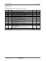
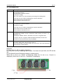
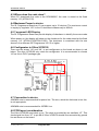
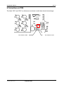
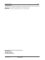
DC6688SLP Manual
Rev3.0
User Manual
for
DC6688SLP
(Former name: SL
Programmer Board ver1.1)
Document Revision 3.0
Aug, 2008
Dragonchip
We bring silicon to life
DragonFLASH
TM
1
DC6688SLP Manual
Rev3.0
Revision History
The following table shows the revision history for this document.
Nov, 2004
Nov, 2004
Dec, 2004
Feb, 2005
Feb, 2005
July, 2005
Aug, 2005
Jan, 2005
July, 2006
July, 2006
Document
Revision
1.0
1.1
1.2
1.3
1.4
1.5
1.6
1.8
1.9
2.0
Sept, 2006
Jan, 2007
2.1
2.2
May, 2007
July, 2007
2.3
2.4
Oct, 2007
May, 2008
Jul, 2008
Jul, 2008
2.5
2.6
2.7
2.8
Date
July, 2008
Aug, 2008
2.9
3.0
Remark
Preliminary for SL Programmer Board ver1.0
Preliminary for SL Programmer Board ver1.1
Modify section 3.1, 4, 5.1, 5.2
added description on DC6688F05S
fix LED flashing for the board, use configurator file “fpga_v1_1.mcs”
Change to use configurator file “fpga_v1_5.mcs”
Change to use configurator file “fpga_v1_10.mcs”
Change to use configurator file “fpga_v1_11.mcs”
Change to use configurator file “fpga_v2_0.mcs”
a) Revise section 2, 3.2, 5.1, 5.2
b) Change to use configurator file “fpga_v2_2.mcs”
Change to use configurator file “fpga_v2_4.mcs”
1) Change to use configurator file “fpga_v2_5.mcs”
2) Revise section 5.2
1) Change to use configurator file “fpga_v2_6.mcs”
1) Change to use configuratot file “fpga_v2_7.mcs”
2) Hardware modified
1) Change to use configurator file “fpga_v2_8.mcs”
1) Change to use configurator file “fpga_v3_0.mcs”
1) Change to use configurator file “fpga_v3_0.mcs” or “fpga_v3_1.mcs”
1) Remove Appendix A
2) Remove Glossary section
3) Added edited by & reviewed by at revision history table
4) Some typing error
Change the name of the board to “DC6688SLP”
Change the name of the board to “DC6688SLP” in all section
Dragonchip
We bring silicon to life
DragonFLASH
TM
Edited By
Reviewed By
-
-
-
-
-
-
-
-
-
-
-
-
-
-
Ken Yeung
Danny Ho
Danny Ho
Danny Ho
Ken Yeung
Ken Yeung
2
DC6688SLP Manual
Rev3.0
Contents
DOCUMENT REVISION 3.0
AUG, 2008 ............................................................................................................1
1 INTRODUCTION ....................................................................................................................................................4
2 DOWNLOAD CODE FROM PC TO DC6688SLP.............................................................................................5
2.1 HARDWARE SETUP ..............................................................................................................................................5
2.2 SOFTWARE SETUP ...............................................................................................................................................6
3 PROGRAMMING DEVICES .................................................................................................................................7
4 HARDWARE DESCRIPTION.............................................................................................................................10
4.1 FUNCTION KEYS ................................................................................................................................................10
4.1.1 DC6688FSA ..........................................................................................................................................10
4.1.2 DC6688FL32A......................................................................................................................................11
4.1.3 DC6688F05S ........................................................................................................................................12
4.1.4 DC6688FLX ..........................................................................................................................................12
4.1.5 DC6688FSX ..........................................................................................................................................12
4.1.6 DC6688FSB ..........................................................................................................................................12
4.1.7 DC6688FLB ..........................................................................................................................................12
4.2 HARDWARE SETTINGS .......................................................................................................................................14
4.3 WHERE DOES THE CODE STORE? .......................................................................................................................15
4.4 MAXIMUM POWER TO DEVICE ..........................................................................................................................15
4.5 7-SEGMENT LED DISPLAY ................................................................................................................................15
4.6 CONFIGURATOR TO XILINX XC2S100 ..............................................................................................................15
4.7 CONNECTION TO DEVICE ...................................................................................................................................15
4.8 PCB LAYOUT CONSIDERATION..........................................................................................................................15
5 PROGRAMMING TIME.......................................................................................................................................17
5.1 DC6688FSA/FSB ............................................................................................................................................17
5.2 DC6688FL32A/DC6688FLB...........................................................................................................................17
5.3 DC6688F05S....................................................................................................................................................17
5.4 DC6688FSX.....................................................................................................................................................17
5.5 DC6688FLX ....................................................................................................................................................17
6 CORRECTION ON PCB .....................................................................................................................................18
Dragonchip
We bring silicon to life
DragonFLASH
TM
3
DC6688SLP Manual
Rev3.0
1 Introduction
The Objective of this document is to provide the user a quick start to evaluate
DC6688SLP. This board is applicable to the following:
1) DC6688F05S
2) DC6688FSA
3) DC6688FSB
4) DC6688FLB
5) DC6688FL32A
6) DC6688FLX
7) DC6688FSX
To program the DC6688 family, it involves 2 steps:
a) Download code from PC to DC6688SLP refer to section 3 for detail
b) Program DC6688 family in each device refer to section 4 for detail
Section 5 describes the hardware in detail.
Section 6 summarizes the difference between versions of configurator file in detail.
It should be noted that this document applies only to DC6688SLP with the configurator
‘XC18V01PC’ programmed with configurator file “fpga_v3_0.mcs” or “fpga_v3_1.mcs”
or with the configurator ‘XC18V01PC’marked with “v3.0”, or “v3.1”.
Dragonchip
We bring silicon to life
DragonFLASH
TM
4
DC6688SLP Manual
Rev3.0
2 Download code from PC to DC6688SLP
To download the code to DC6688SLP, it involves the hardware and software setup.
Setting up the hardware first, and then use software to control the download.
2.1 Hardware setup
The procedure is listed below:
a) Connect the board via a parallel port cable to PC as shown in diagram 3.1
b) Attach a fixed power supply to the power-connector at ‘J13’. An unregulated +7.5V
up to +12V/800mA power source can be used to supply the power of the board. The
correct polarity of the power plug is shown in diagram 3.2.
c) Turn on the switch ‘S1’. The LED ‘D14’should turn on to indicate the board is ready.
The on/off position is shown in diagram 3.3
PC
To parallel port
in PC side
DC6688SLP
Diagram 3.1 Connection between SL
Programmer board and PC
+ve (inside)
Polarity : -ve (outside)
Diagram 3.2 Polarity of DC Jack
ON
OFF
Diagram 3.3 On/Off position of power
switch
Dragonchip
We bring silicon to life
DragonFLASH
TM
5
DC6688SLP Manual
Rev3.0
2.2 Software setup
The software setup needs ‘Dragonchip ISP Programmer’ with version 4.1.0 or higher.
Details on setup and how to use the software to download code refer to document
“Dragonchip In-system programmer Manual”. This software downloads the code to
DC6688SLP.
After downloading the code, the checksum displayed on the 7-segment LEDs is not
updated until turning off/on the power.
Dragonchip
We bring silicon to life
DragonFLASH
TM
6
DC6688SLP Manual
Rev3.0
3 Programming devices
The procedure is listed below:
1. Connect the board to each device as shown in diagram 4.1. Use connector ‘J1’ to
‘J10’to connect to each device. The pin assignment on each connector is shown in
diagram 4.2.
The SL Programmer board can support up to 10 devices. For example, if only 6
devices are needed to program, then the connectors ‘J1’to ‘J6’are used.
Buzzer
Device 1
Device 2
Device 3
Device 4
Device 5
DC6688SLP
Device 6
Device 7
Device 8
Device 9
Device
Diagram 4.1 Connection between SL
Programmer board and device
GND
ISPSEL
PWR
GND
ISPSEL
PWR
GND
ISPSEL
PWR
GND
ISPSEL
PWR
GND
ISPSEL
PWR
GND
ISPSEL
PWR
GND
ISPSEL
PWR
GND
ISPSEL
PWR
GND
ISPSEL
PWR
GND
ISPSEL
PWR
Diagram 4.2 Pin assignments for each
connector ‘J1’– ‘J10’
Dragonchip
We bring silicon to life
DragonFLASH
TM
7
DC6688SLP Manual
2.
Rev3.0
Connect a 3VDC buzzer to ‘J15’on the board. This buzzer produces beep sounds.
It provides an alternative to user a notice that the 10 devices finish programming
no matter success or failure. Below is a table to show how to use buzzer according
to different number of devices to be program for each turn:
For example: there are 2 devices to be programmed for each turn. It can be found in
the table that connector ‘J1’ – ‘J2’ will be used. A connection between the point
‘BUZZAR_TEST_PAD’ and LED3 should be made. Then each time finished
programming, the buzzer beeps sound immediately.
No. of
devices to
program
connector
to device
Buzzer connection[1]
1
‘J1’
a) open the connection on ‘R58’, and
b) make a connection between the point ‘BUZZAR_TEST_PAD’and
LED2
2
‘J1’- ‘J2’
a) open the connection on ‘R58’, and
b) make a connection between the point ‘BUZZAR_TEST_PAD’and
LED3
3
‘J1’- ‘J3’
a) open the connection on ‘R58’, and
b) make a connection between the point ‘BUZZAR_TEST_PAD’and
LED4
4
‘J1’- ‘J4’
a) open the connection on ‘R58’, and
b) make a connection between the point ‘BUZZAR_TEST_PAD’and
LED5
5
‘J1’- ‘J5’
a) open the connection on ‘R58’, and
b) make a connection between the point ‘BUZZAR_TEST_PAD’and
LED6
6
‘J1’- ‘J6’
a) open the connection on ‘R58’, and
b) make a connection between the point ‘BUZZAR_TEST_PAD’and
LED7
7
‘J1’- ‘J7’
a) open the connection on ‘R58’, and
b) make a connection between the point ‘BUZZAR_TEST_PAD’and
LED8
8
‘J1’- ‘J8’
a) open the connection on ‘R58’, and
b) make a connection between the point ‘BUZZAR_TEST_PAD’and
LED9
9
‘J1’- ‘J9’
a) open the connection on ‘R58’, and
b) make a connection between the point ‘BUZZAR_TEST_PAD’and
LED10
10
‘J1’- ‘J10’
short the connection on ‘R58’
Remarks:
[1] R58, ‘BUZZAR_TEST_PAD’, LED1 - LED10 are shown on schematics ‘CASE’
Dragonchip
We bring silicon to life
DragonFLASH
TM
8
DC6688SLP Manual
3.
4.
5.
6.
7.
8.
Rev3.0
Check the settings on the board. Details refer to section 5.2
Attach a fixed power supply to the power-connector at ‘J13’. An unregulated +7.5V
up to +12V/800mA power source can be used to supply the power of the board.
The correct polarity of the power plug is shown in diagram 3.2.
Turn on the switch ‘S1’. The LED ‘D14’ should turn on to indicate the board is
ready. The 7-segment LED shows up the checksum.
After displayed the checksum, press ‘Auto’button to do programming.
After hearing the buzzer beeping sounds, it indicates programming finished. All the
devices can unplug without switching off power. If the devices need to reprogram(‘Auto’button), verify(‘Verify’button) or read checksum(‘Checksum’button),
the devices should unplug and plug again.
Repeat step 1 to 7 for the second turn programming. Step 2 – step 5 can be
skipped. When reaching step 6, press the ‘Auto’ button no matter the programmer
still undergo last turn programming. For example, assuming that there is only 1
device to program for each turn. The programmer still goes to program the rest of 9
devices. When pressing ‘Auto’ button, the device being programming will continue
until finish. The programmer then goes to restart from device 1.
Dragonchip
We bring silicon to life
DragonFLASH
TM
9
DC6688SLP Manual
Rev3.0
4 Hardware description
4.1 Function keys
4.1.1 DC6688FSA
Keys
Description
Auto
This key performs
a) write code to device,
b) read back the code from device,
c) verify the code[2],
d) if ‘Lock’switch is on, lock the device preventing from reading back
From step a to d, the LED corresponding to a device will flash.
If the result success, the LED turns on.
If the result fails, the LED turns off.
Verify
This key performs
a) read back the code from device,
b) verify the code[2]
From step a to b, the LED corresponding to a device will flash.
If the result success, the LED turns on.
If the result fails, the LED turns off.
CheckSum[1] This key performs
a) read back the Model, Version, Checksum stored at 0x3A ~ 0x3F in data
flash memory on device 1(i.e. connector “J1”)
b) display the Model, Version, Checksum on the four 7-segment LEDs
On step b, the four 7-segment LEDs will display the Model, Version and
Checksum in the order and then recycle again[3].
Reset
This key, when pressed, will reset the board to initial state without turn off/on
the power. When ready, the LED ‘D14’turns on.
It is recommended to use power switch ‘S2’to do reset. This is also equivalent
to the function of ‘Reset’button.
Remarks:
[1] Only device 1 will be read for checksum.
[2] Verify the code by comparing byte by byte. If at least one byte fails, the LED will be
off.
[3] The Model/Version/Checksum display is shown below:
When the 1st dot is on, ‘Model’ is displaying. When the 2nd dot is on, ‘Version’ is
displaying. When the 3rd dot is on, ‘Checksum’is displaying.
Dragonchip
We bring silicon to life
DragonFLASH
TM
10
DC6688SLP Manual
Rev3.0
4.1.2 DC6688FL32A
Keys
Description
Auto
This key performs
a) write code to device,
b) read back the code from device,
c) verify the code[2],
d) if ‘Lock’switch is on, lock the device preventing from reading back
From step a to d, the LED corresponding to a device will flash.
If the result success, the LED turns on.
If the result fails, the LED turns off.
Verify
This key performs
a) read back the code from device,
b) verify the code[2]
From step a to b, the LED corresponding to a device will flash.
If the result success, the LED turns on.
If the result fails, the LED turns off.
CheckSum[1] This key performs
a) read back the Model, Version, Checksum in flash memory on device 1 (i.e.
connector “J1”)
b) display the Model, Version, Checksum on the four 7-segment LEDs
On step b, the four 7-segment LEDs will display the Model, Version and
Checksum in the order and then recycle again[3].
Reset
This key, when pressed, will reset the board to initial state without turn off/on
the power. When ready, the LED ‘D14’turns on.
It is recommended to use power switch ‘S2’to do reset. This is also equivalent
to the function of ‘Reset’button.
Remarks:
[1] Only device 1 will be read for checksum.
[2] Verify the code by comparing byte by byte. If at least one byte fails, the LED will be
off.
[3] The Model/Version/Checksum display is shown below:
When the 1st dot is on, ‘Model’ is displaying. When the 2nd dot is on, ‘Version’ is
displaying. When the 3rd dot is on, ‘Checksum’is displaying.
Dragonchip
We bring silicon to life
DragonFLASH
TM
11
DC6688SLP Manual
Rev3.0
4.1.3 DC6688F05S
Keys
Description
Auto
Verify
CheckSum[1]
Reset
Refers to section 4.1.2 for details
Refers to section 4.1.2 for details
Refers to section 4.1.2 for details
Refers to section 4.1.2 for details
Remarks:
[1] Only device 1 will be read for checksum.
4.1.4 DC6688FLX
Keys
Description
Auto
Verify
CheckSum[1]
Reset
Refers to section 4.1.2 for details
Refers to section 4.1.2 for details
Refers to section 4.1.2 for details
Refers to section 4.1.2 for details
Remarks:
[1] Only device 1 will be read for checksum.
4.1.5 DC6688FSX
Keys
Description
Auto
Verify
CheckSum[1]
Reset
Refers to section 4.1.2 for details
Refers to section 4.1.2 for details
Refers to section 4.1.2 for details
Refers to section 4.1.2 for details
Remarks:
[1] Only device 1 will be read for checksum.
4.1.6 DC6688FSB
Keys
Description
Auto
Verify
CheckSum[1]
Reset
Refers to section 4.1.1 for details
Refers to section 4.1.1 for details
Refers to section 4.1.1 for details
Refers to section 4.1.1 for details
Remarks:
[1] Only device 1 will be read for checksum.
4.1.7DC6688FLB
Keys
Description
Auto
Verify
CheckSum[1]
Reset
Refers to section 4.1.2 for details
Refers to section 4.1.2 for details
Refers to section 4.1.2. for details
Refers to section 4.1.2 for details
Dragonchip
We bring silicon to life
DragonFLASH
TM
12
DC6688SLP Manual
Rev3.0
Remarks:
[1] Only device 1 will be read for checksum.
Dragonchip
We bring silicon to life
DragonFLASH
TM
13
DC6688SLP Manual
Rev3.0
4.2 Hardware settings
DIP switch ‘SW6’have the following setting:
The following settings apply to only configurator XC18V01 with “fpga_v3_0.mcs” or
“fpga_v3_1.mcs”, or marked with v3.0, or v3.1.
Position Device
1
Mode of XC2S100
On: Master (default)
Off: JTAG
User should not modify this setting
2, 3
Frequency selection:
SW2
SW3
ON
ON
Fosc/12 = 4MHz
ON
OFF
Fosc/8 = 6MHz
OFF
ON
Fosc/1
OFF
OFF
Fosc/4 = 12MHz (default)
Program device selection
SW4
SW5
SW6
SW7
ON
ON
ON
ON
DC6688F05S/SP/SN
ON
ON
ON
OFF
DC6688F2SB/SBT
DC6688F4SB/SBT/SA
ON
ON
OFF
ON
DC6688F8SB/SBT/SA
ON
ON
OFF
OFF
DC6688F14SB/SBT
DC6688F16SB/SBT/SA
ON
OFF
ON
ON
DC6688F24SB/SBT/SA
(default)
ON
OFF
ON
OFF
DC6688F30SB/SBT/SBE/SA
ON
OFF
OFF
ON
DC6688FE4
ON
OFF
OFF
OFF
DC6688FE8
OFF
ON
ON
ON
DC6688FE16
OFF
ON
ON
OFF
DC6688FE24
OFF
ON
OFF
ON
DC6688FL32A
DC6688FL16B/BT
OFF
ON
OFF
OFF
reserved
OFF
OFF
ON
ON
DC6688F62SX/SXE/SXR
OFF
OFF
ON
OFF
DC6688FL64X/XE
OFF
OFF
OFF
ON
reserved
OFF
OFF
OFF
OFF
reserved
Lock
This key decides to lock DC6688FSA, DC6688FSB, DC6688FL32A,
DC6688FLB and DC6688F05S when pressing ‘Auto’button
On: lock(program flash memory) enable (default)
Off: no lock
4, 5, 6, 7
8
This key decides to lock DC6688F62SX/SXE/SXR when pressing ‘Auto’
button
On: lock(program flash memory only) enable (default)
Off: no lock
This key decides to lock DC6688FL64X/XE when pressing ‘Auto’button
On: lock(program flash memory and data flash memory) enable (default)
Off: no lock
Dragonchip
We bring silicon to life
DragonFLASH
TM
14
DC6688SLP Manual
Rev3.0
4.3 Where does the code store?
When PC downloads the code to the DC6688SLP, the code is stored to the flash
memory ‘U3’(AT29LV512).
4.4 Maximum Power to device
The SL Programmer Board ver1.0 can support up to 10 devices. The maximum current
to supply by regulator ‘U10’to the 10 devices simultaneously is 800mA.
4.5 7-segment LED Display
The SL Programmer Board can provide display of checksum to identify the source code.
When power on, the display will show up the checksum for the code stored at the flash
memory ‘U3’ (AT29LV512/AT29LV010A). The checksum is consistent with the one
shown in the software ISP Programmer V3.5.5 or higher.
4.6 Configurator to Xilinx XC2S100
There are two areas, ‘U6’ and ‘U8’, to put configurator on the board as shown in red
below. The xilinx XC2S100 only need one configurator. It is recommended to choose
‘U6’as this is PLCC package type.
4.7 Connection to device
AWG#26 wire is recommended for power line. The wire, which the thickness is too thin,
is not appropriate.
AWG#28 wire is recommended for ISPSEL line.
4.8 PCB layout consideration
The Xilinx XC2S100 need clock to run. The clock is provided by can oscillator ‘U7’. This
clock signal line from ‘U7’to pin 88 of Xilinx XC2S100 should be surrounded by ground
line as shown on the board.
Dragonchip
We bring silicon to life
DragonFLASH
TM
15
DC6688SLP Manual
Rev3.0
To reduce noise on the board, both sides of the 2-layer PCB should be poured with
ground copper wherever space is available as shown on the board.
Dragonchip
We bring silicon to life
DragonFLASH
TM
16
DC6688SLP Manual
Rev3.0
5 Programming Time
5.1 DC6688FSA/FSB
The maximum programming time for each device operating at 12MHz is shown in the
table below:
Program Size/kbytes
2
4
8
14
16
24
30
Programming time/s
0.850
0.850
1.340
2.330
2.330
3.320
4.070
5.2 DC6688FL32A/DC6688FLB
The maximum programming time for each device operating at 12MHz is 4.400s
5.3 DC6688F05S
The maximum programming time for each device operating at 4MHz is 3.840s
5.4 DC6688FSX
The maximum programming time for each device operating at 12MHz is shown in the
table below:
Devices
DC6688F62SX/SXE/SXR
Programming time/s
8.000
5.5 DC6688FLX
The maximum programming time for each device operating at 12MHz is shown in the
table below:
Devices
DC6688FL64X/XE
Dragonchip
We bring silicon to life
DragonFLASH
Programming time/s
8.240
TM
17
DC6688SLP Manual
Rev3.0
6 Correction on PCB
The label “R23” and “R56” on silkscreen as shown in red below should interchange.
This resistor is R23
This resistor is R56
Dragonchip
We bring silicon to life
DragonFLASH
TM
18
DC6688SLP Manual
Rev3.0
Copyright Notice
This specification is copyrighted by Dragonchip Ltd. No part of this specification may be reproduced in
any form or means, without the expressed written consent Dragonchip Ltd.
Disclaimer
Dragonchip Ltd. assumes no responsibility for any errors contained herein.
Copyright by Dragonchip Ltd. All Rights Reserved.
Dragonchip Ltd.
TEL: (852) 2776-0111
FAX: (852) 2776-0996
http://www.dragonchip.com
Dragonchip
We bring silicon to life
DragonFLASH
TM
19